
 Open Access Article
 This Open Access Article is licensed under a Creative Commons Attribution-Non Commercial 3.0 Unported Licence
Low temperature synthesis of photoconductive BaSi2 films via mechanochemically assisted close-spaced evaporation†
Kosuke O.
Hara
 *a,
Chiaya
Yamamoto
b,
Junji
Yamanaka
b and
Keisuke
Arimoto
a
*a,
Chiaya
Yamamoto
b,
Junji
Yamanaka
b and
Keisuke
Arimoto
a
aCenter for Crystal Science and Technology, University of Yamanashi, Kofu, Yamanashi 400-8511, Japan. E-mail: khara@yamanashi.ac.jp; Fax: +81 55 220 8270; Tel: +81 55 220 8614
bCenter for Instrumental Analysis, University of Yamanashi, Kofu, Yamanashi 400-8510, Japan
First published on 6th September 2021
Abstract
BaSi2 is an emerging photovoltaic material with optimum optoelectronic properties and can be deposited by close-spaced evaporation, which has the advantages of epitaxial growth, high productivity, and scalability to large area deposition. This process is enabled by two reactions: (1) Ba gas generation from a milled BaAl4–Ni source and (2) BaSi2 formation from the Ba gas and a Si substrate, and is limited by the temperature of the former reaction. We show that mechanical activation of the BaAl4–Ni source by ball milling within 60 s lowers the BaSi2 film synthesis temperature down to 700 °C from 1000 °C required for the source ground using a pestle and mortar. Interestingly, additional milling beyond 60 s reduces the Ba gas generation rate, presumably because Ni is mechanochemically dissolved into BaAl4. The BaSi2 films synthesized at 700 °C are free from cracks and are epitaxially grown with (100) orientation on Si(100) substrates. Hall effect measurements reveal low electron concentration below 1.1 × 1017 cm−3. Photoconductance of the BaSi2 films correlates with film thickness, clearly indicating photocarrier generation in BaSi2. Thus, the mechanochemically assisted synthesis opens the way for solar cell applications of BaSi2 films synthesized via close-spaced evaporation.
1 Introduction
Solar cells have rapidly penetrated into our society in the last decade due to the demand for renewable power sources. Crystalline Si solar cells account for more than 90% of manufactured cells owing to their high efficiency and device stability, and the well-established Si industry. However, indirect-gap Si suffers from inefficient optical absorption, which necessitates a thick crystal of ≥100 μm.1 Barium disilicide (BaSi2) possesses high optical absorption coefficients (≥104 cm−1 for photon energies over bandgap (Eg)),2,3 facilitating low-cost thin-film architecture for solar cell applications. Moreover, Eg of BaSi2 (1.3 eV2–4) is optimum for single-junction solar cells with a theoretical limit of 33% under AM1.5 illumination.5,6 A long minority-carrier lifetime up to 27 μs7,8 and diffusion length up to 10 μm9,10 reflect a high potential toward high efficiency cells. The abundance of Ba and Si resources in the earth's crust assures large-scale deployment potential. So far, pn homojunction BaSi2 cells have been reported with a power conversion efficiency of 0.28%.11 Heterojunctions of p-type BaSi2 and n-type Si have also been reported with a higher efficiencies of up to 9.9%.12Close-spaced evaporation (CSE) is an efficient and high-quality process that can produce BaSi2 epitaxial films on Si substrates.13 In this process, a Si substrate and a planar BaAl4–Ni powder source are heated at the same temperature in a vacuum. At high temperatures, BaAl4 and Ni react to produce Ni–Al compounds and Ba gas,14,15 the latter of which reacts with the Si substrate to produce a BaSi2 film. Because films can be synthesized using a rapid thermal annealing system, CSE has the advantages of high productivity and scalability for large area deposition. In a previous study, epitaxial BaSi2 films were synthesized with a largest single orientation area among the previously reported BaSi2 films,13 which indicates high crystallinity of the CSE BaSi2 films. Epitaxial growth was also observed in CaGe2 films deposited by CSE.16 In a previous CSE study of BaSi2,13 however, the film deposition temperature was limited to 1000 °C. Due to the large thermal stress, the films were cracked, which hindered electrical characterization and applications. If the deposition temperature could be lowered, electrical characterization and solar cell applications would become possible.
Mechanochemistry can potentially serve to lower the deposition temperature. The most famous mechanochemical phenomenon may be a mechanochemical reaction, which realizes materials synthesis by ball milling without external heating.17 A reaction is completed by mechanical mixing at atomic levels or by accumulating defect energy above the activation energy. In metallurgy, it is also called mechanical alloying.18 Recently, mechanochemical reaction has attracted attention as an excellent way to greatly reduce or even completely avoid solvent use.19 Another important mechanochemical effect is the mechanical activation that lowers the reaction temperature by ball milling. Before mechanochemical reaction occurs, materials accumulate internal and surface energy by producing various types of defects and by increasing the surface area, which results in the increased ability for reaction.17 A wide variety of materials were synthesized at lower temperatures compared to those using conventional solid-state reaction routes by mechanical activation such as alloys20 and complex oxides.21
Here, we improve the CSE process by taking advantage of mechanochemical phenomena, which have not been used in vacuum vapor deposition processes partly because chemical reactions are not expected in the source in conventional processes. CSE is an attractive playground where the powder and vacuum vapor deposition processes meet. In this study, our objective is threefold. Firstly, we investigate whether the film synthesis temperature can be lowered by the mechanochemical treatment of the BaAl4–Ni source. Synthesis temperature will be shown to be lowered down to 700 °C with an optimum milling condition. The reason why the optimum condition exists is also elucidated. Secondly, we show that cracking is suppressed at low temperatures. Finally, electrical and photoconductive properties of crack-free BaSi2 films are investigated. The results demonstrate low electron concentration enough for device applications and the photoconductance correlated positively with BaSi2 thickness.
2 Experimental
Commercial BaAl4 powder (>99.5% in purity, Kojundo Chemical Laboratory) and Ni powder (99.9% in purity, ca. 2–3 μm, Kojundo Chemical Laboratory) were mixed with a BaAl4/Ni molar ratio of 1/4 and were milled in a vibratory ball mill (P-23, FRITSCH) at 50 Hz for 10–1200 s. Balls (5 mm in diameter) and the milling vessel (10 ml) were made of zirconia. The ball-to-powder weight ratio was 1/100. Milled BaAl4–Ni powder and a Si(100) substrate were closely placed via a 2 mm-thick quartz spacer on Si wafers, as shown in Fig. 1. Weights of BaAl4–Ni powders were 1 and 6.3 mg for 10 and 18 mm substrates, respectively. Four kinds of Si(100) wafers were used as substrates: (1) As-doped n-type wafers (0.001–0.005 Ω cm) for investigating the effects of milling time, (2, 3) P-doped n-type wafers (0.141–0.208 and ≥1000 Ω cm) for structural characterization after deciding the optimum milling time, and (4) B-doped p-type wafers (≥1000 Ω cm) for electrical and photoconductive characterization. On the Si(100) substrate, a 2 mm-thick quartz plate was placed as a weight. All jigs and substrates were cleaned with acetone, methanol, and deionized water. The Si substrate and the upper source holder were further cleaned with diluted HF solution in the investigation using the optimum milling time. The whole setup was evacuated below 2 × 10⁻⁴ Pa by a turbo molecular pump and a diaphragm pump and was heated in a rapid thermal annealing system (MILA-5000, ADVANCE RIKO). The setup was degassed at 200 °C for 90 min. After that, temperature was increased to 600–900 °C and was kept for 2.5–50 min. The heating rate was 2 °C s−1 above 200 °C while the nominal cooling rate was 20 °C s−1.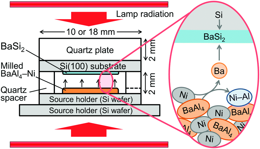 | ||
| Fig. 1 A schematic drawing of BaSi2 film synthesis by CSE. | ||
The prepared samples were characterized by X-ray diffraction (XRD; Discover D8, Bruker), scanning electron microscopy (SEM; TM3030, Hitachi; S-5200, Hitachi), transmission electron microscopy (TEM; Tecnai Osiris, FEI), Hall effect measurements (ResiTest8308, TOYO), and photoconductance measurements. Two dimensional (2D) XRD patterns were collected using an area detector and 1 mm-collimated, Ni-filtered Cu Kα radiation by scanning the ω axis, which were converted to one-dimensional (1D) patterns by integrating along the χ axis. SEM backscattered electron (BE) images were taken on a TM3030 at an acceleration voltage of 15 kV while secondary electron (SE) images were recorded on a S-5200 at an acceleration voltage of 5 kV. High-angle annular dark-field scanning transmission electron microscopy (HAADF-STEM) images were obtained at an acceleration voltage of 200 kV. Energy-dispersive X-ray spectroscopy (EDX) was also performed with TM3030 and Tecnai Osiris. Hall effect measurements were performed using the van der Pauw geometry with a 0.44 T electromagnet. Four circular 150 nm-thick Al contacts were formed on the film surface via radio-frequency magnetron sputtering. The photoconductive properties were characterized by measuring current–voltage characteristics under dark and optical irradiation. Current–voltage characteristics were measured through the Al contacts for the Hall effect measurements using a Keithley 2450 source meter. The AM1.5 illumination was provided by a solar simulator (XES-40S2-CE, San-ei Electric).
3 Results and discussion
3.1 Investigations on mechanochemical effects
Fig. 2 compares the morphology of ball-milled BaAl4–Ni powders with the powder ground using a pestle and mortar, which was used in the previous study.13 The Ni powder used for grinding contained larger particles of <10 μm than in this study. The as-purchased BaAl4 powder consists of even larger particles, which are easily distinguishable by EDX [ESI,† Fig. S1(a)], as indicated in Fig. 2(a). After ball milling for 60 s, BaAl4 particles become small and mix with Ni particles. BaAl4 and Ni cannot be distinguished from Fig. 2(b) even using EDX [Fig. S1(b), ESI†]. With increasing milling duration to 150 s, particle size does not apparently change from 60 s. After 1200 s milling, the powder consists of obviously minute particles below 20 μm. Thus, ball milling can produce more mixed BaAl4–Ni powders within 60 s at 50 Hz than grinding. However, it takes 1200 s to pulverize the powder into minute particles.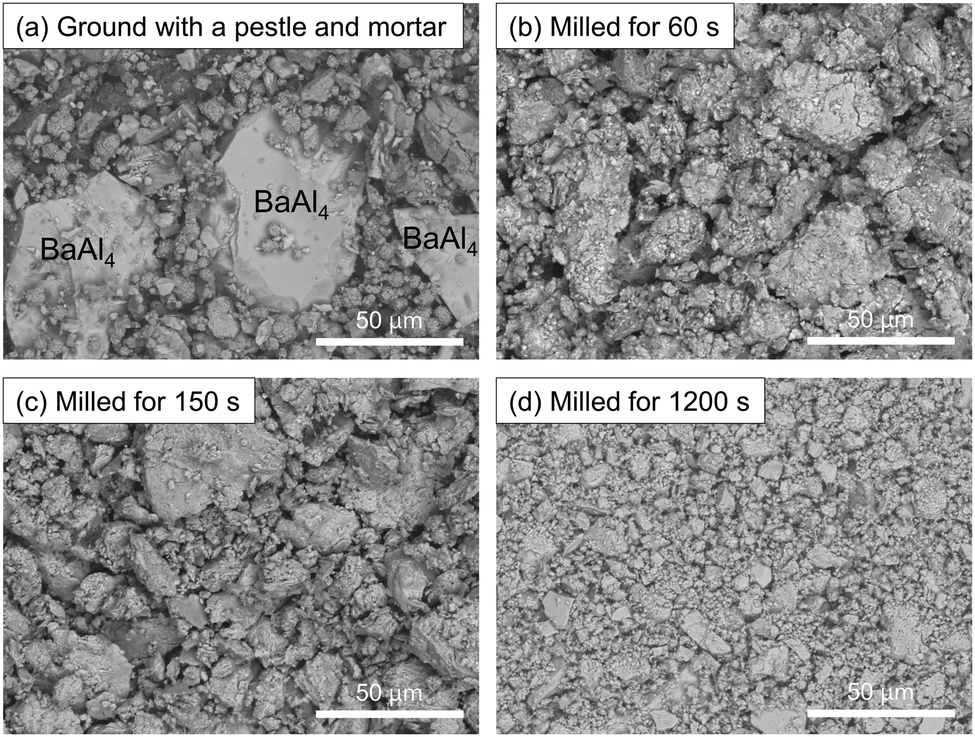 | ||
| Fig. 2 BE images of as-ground and as-milled BaAl4–Ni powder sources. | ||
Fig. 3 shows XRD patterns of the CSE films synthesized using the BaAl4–Ni powder milled for 60 s. Displayed are 1D patterns generated from 2D patterns obtained by the area detector. The powder pattern of BaSi2 calculated using the reported structure data22 is also shown. The sample prepared at 600 °C for 5 min does not exhibit peaks, indicating that a BaSi2 film is not synthesized. On the other hand, CSE at 700 °C yields a film exhibiting clear peaks corresponding to orthorhombic BaSi2. Upon increasing the temperature to 900 °C, the BaSi2 peaks become strong, which suggests that BaSi2 films grow thick. It is also noted that the relative intensity significantly differs from the powder pattern. This is because the films grow epitaxially, as is evidenced by the spotty 2D pattern displayed as an inset. The 2D pattern shows that the film is a (100) oriented epitaxial film. This preferred orientation is the same as the BaSi2 films synthesized by molecular beam epitaxy (MBE)23,24 and thermal evaporation,25,26 while it differs from the preferred (001) orientation of the CSE films synthesized at 1000 °C.13 The factors deciding the preferred orientation of CSE BaSi2 films are an interesting topic for future studies.
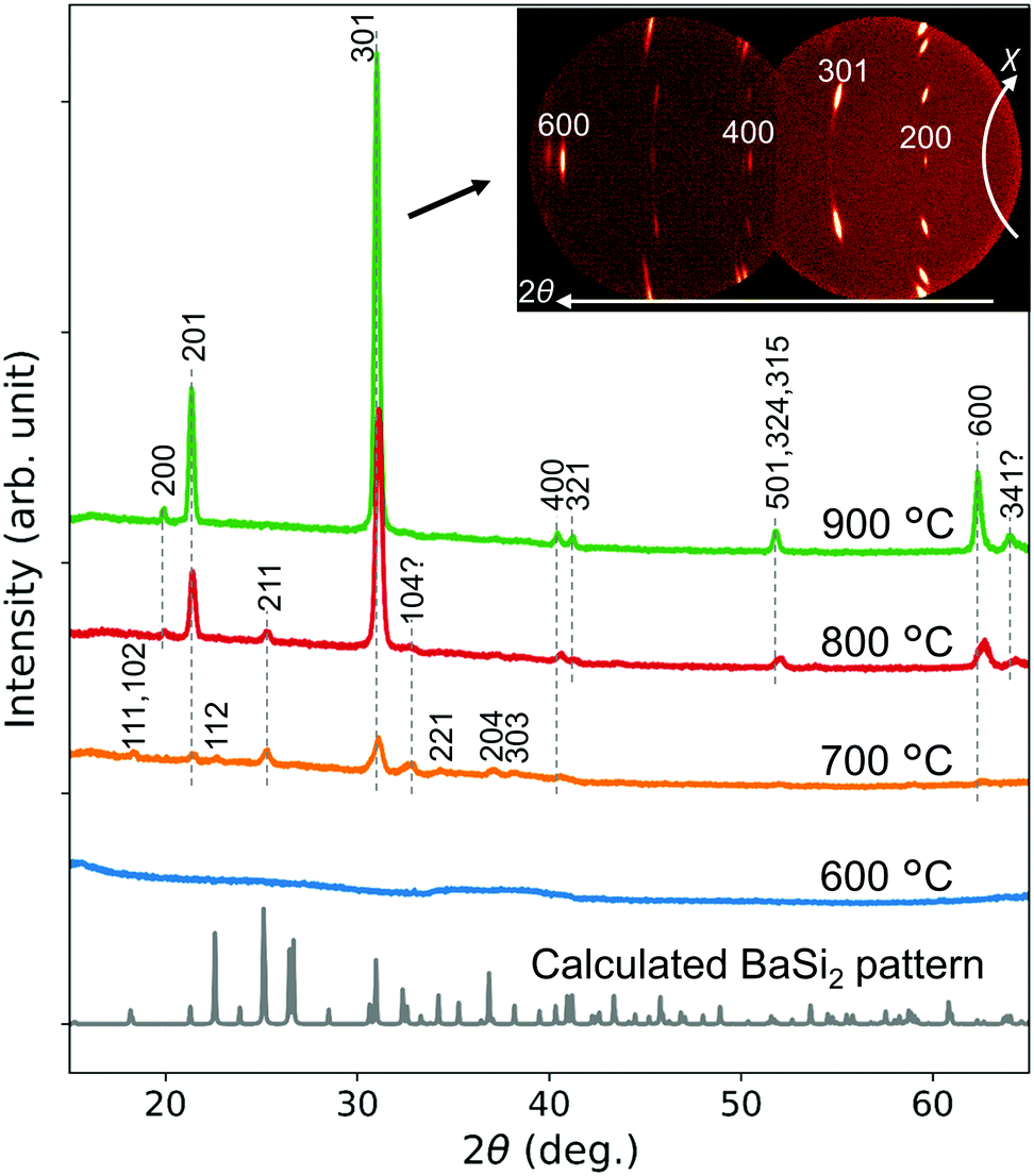 | ||
| Fig. 3 1D XRD patterns generated from 2D patterns of CSE films synthesized at 600–900 °C for 5 min. The BaAl4–Ni source milled for 60 s was used. Also displayed is a calculated powder pattern of orthorhombic BaSi2 based on the structure data reported by Goebel et al.22 | ||
For quantitatively and efficiently analyzing the deposited amount of Ba atoms, we measured the composition of the CSE samples on their surfaces by EDX. Fig. 4 shows the Ba/Si ratios for CSE at 800 and 900 °C for 5 min as a function of milling time. Because the X-ray escape depth (∼1.5 μm) is larger than the film thickness, which is shown in the ESI,† Fig. S2, the measured Ba/Si ratio is not the film composition but is positively correlated with the total Ba deposition amount. Fig. 4 hence indicates that the Ba deposition amount increases with milling time and reaches a maximum at 60 s, and suddenly decreases after that. This tendency appears at both 800 and 900 °C, though the absolute value is larger at 900 °C than 800 °C. Thus, a milling time of 60 s is optimum for BaSi2 deposition under the current conditions. The enhanced Ba generation by ball milling is clearly attributed to the mechanochemical effect. That is, the Ba gas generation rate is enhanced by mechanical activation through the increase in the BaAl4–Ni contact area and in the internal energy due to defects. On the other hand, when the source is milled for 1200 s, the Ba/Si ratio decreases to almost zero, meaning that the source hardly generates Ba gas after prolonged milling. This result suggests that the BaAl4–Ni source chemically changes after milling for over 60 s.
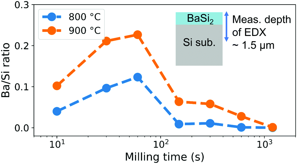 | ||
| Fig. 4 Ba/Si ratios as an indicator of the Ba deposition amount for CSE samples prepared at 800 and 900 °C for 5 min. The composition was measured on the surfaces and is shown as a function of milling time. | ||
The milled source powders were analyzed by XRD, the result of which is shown in Fig. S3, ESI.† BaAl4 peaks become broad by milling and finally become undetectable after milling of 600 s. Ni peaks similarly become broad, but remain after milling for 1200 s. Besides these changes, no chemical reactions were detected.
We further analyzed the milled powders by TEM. Fig. 5 compares the elemental distribution in powder particles milled for (a) 60 and (b) 150 s. The observed particle after milling for 60 s homogeneously contains Ba and Al, indicating a BaAl4 particle. Ni is not found in this particle. On the other hand, after 150 s milling (b), Ni is found in a BaAl4 particle, suggesting that Ni dissolves in BaAl4. We observed seven and six particles from the powders milled for 60 and 150 s, respectively. All of them exhibited similar elemental distributions. Distribution of Ni, thus, significantly changes between 60 and 150 s of milling. Specifically, mechanochemical reaction or mechanical alloying may occur by milling over 60 s.
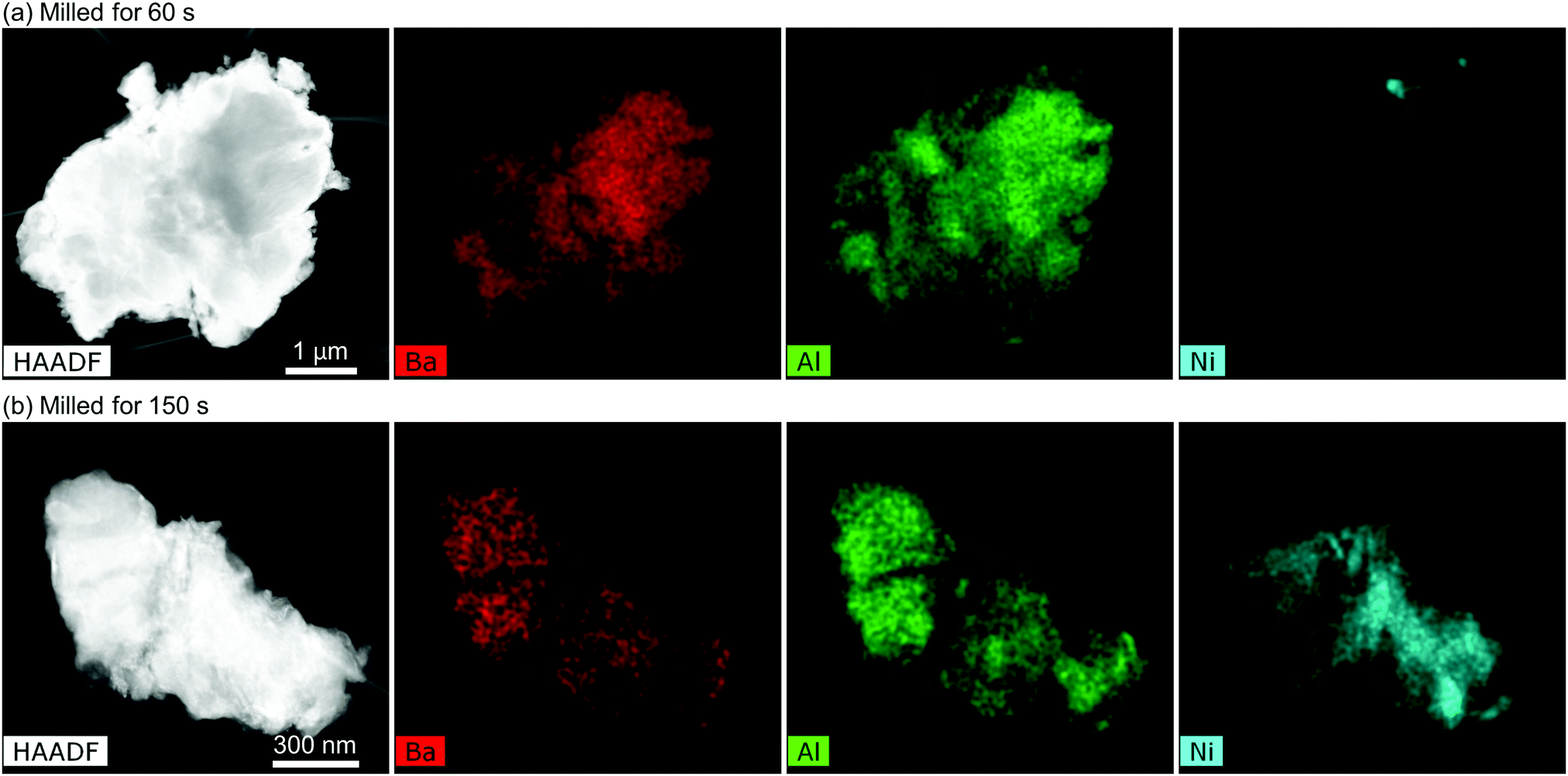 | ||
| Fig. 5 HAADF-STEM images and corresponding EDX elemental mapping of the BaAl4–Ni powders milled for (a) 60 and (b) 150 s. | ||
If Ni dissolves in BaAl4, the lattice parameters of BaAl4 could change. However, it was difficult to detect peak shifts from XRD patterns due to considerable peak broadening (ESI,† Fig. S3). It is also possible that Ba and Al dissolve in Ni at the same time. We mixed the milled BaAl4–Ni powders with a Si powder as an internal standard and measured them via XRD with a scintillation detector (ESI,† Fig. S4). The analyzed lattice parameters of Ni did not significantly change with different milling times. Ba and Al dissolution in Ni is hence negligible.
Thus, Ni is incorporated into BaAl4 particles after 150 s of milling in some form. Because the Ba deposition amount drops after 150 s of milling (Fig. 4), this Ni incorporation seems to play a significant role in the Ba gas generation reaction. Because the main driving force of Ba gas generation is probably the large formation enthalpy of Ni–Al compounds, Ni–Al bonding formed by prolonged milling may account for the reduced Ba gas generation. Actually, the reaction products of CSE changes from Ni3Al and BaAl2O4 to NiAl as milling time increases (ESI,† Fig. S5). This observation supports the idea that different reactions are preferred to Ba gas generation reaction after long milling time.
In short, ball milling of the BaAl4–Ni source first enhances the Ba gas generation rate through mechanical activation. This is probably because of the increase in the contact area between BaAl4 and Ni resulting from particle size reduction and fine mixing [Fig. 2 and Fig. S1, ESI†] and because of the increased internal energy due to defects. Additional ball milling causes a mechanochemical reaction that prevents the Ba gas generation reaction. This is presumably owing to the decrease in the driving force of the Ba gas generation reaction through Ni–Al bond formation. Ba gas generation can, therefore, be promoted by mechanical activation as long as a mechanochemical reaction does not start.
3.2 Synthesis and characterization of crack-free films
Mechanochemical effects maximize the Ba gas generation rate by ball milling for 60 s under the present milling conditions. We therefore fixed milling time to 60 s and attempted to synthesize crack-free BaSi2 films. Fig. 6 compares SEM images of the surface of CSE films synthesized at 700, 800, and 900 °C for 5 min using the 60 s milled source. The 900 °C synthesized film is obviously cracked. This cracking is similar to the films synthesized at 1000 °C in the previous study13 and is owing to a large tensile stress induced in the film during cooling.27 The tensile stress is relieved by cracking.27 The 800 °C synthesized film also shows lines on its surface. However, they are narrower than the cracks on the 900 °C film. With decreasing CSE temperature to 700 °C, no more lines are visible on the surface, which shows that crack-free films are successfully synthesized. The crack-free films involve in-plain tensile stress and out-of-plain compressive stress, which can be detected by XRD. As can be seen in Fig. 3, out-of-plain 400 and 600 peaks obviously shift to higher angles for the 700 and 800 °C samples than the 900 °C sample that is relaxed by cracking. Thus, the CSE films synthesized at not only 700 but also 800 °C involve in-plain tensile stress, meaning that the films are not cracked. The lines on the 800 °C film possibly correspond to valley morphology or low-density regions with voids. At least, each domain separated by lines is connected so that the in-plain stress can be retained.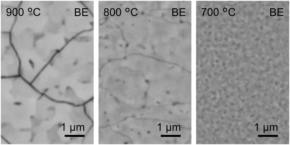 | ||
| Fig. 6 Surface SEM images of the CSE films synthesized at 700, 800, and 900 °C for 5 min using 60 s milled sources. | ||
For investigating the growth kinetics and the maximum thickness of crack-free films, we prepared CSE films at 700 °C by varying the growth time. Fig. 7(a)–(e) shows the SEM images of the cleaved cross-sections of the CSE films synthesized for 2.5–50 min at 700 °C. Within 2.5 min, BaSi2 crystal islands are formed [Fig. 7(a)]. The island height is around 70 nm. Except the islands, the substrate is not covered or covered with a very thin film of <10 nm. These islands coalesce within 5 min, resulting in a continuous film [Fig. 7(b)]. The boundaries where the neighboring islands coalesced are observed as surface pits. After 7.5 min, the film becomes flat and increases its thickness as growth time increases [Fig. 7(c) and (d)]. The film surface, however, becomes rough after 50 min of CSE [Fig. 7(e)]. This surface roughening is possibly owing to re-evaporation of deposited atoms. As found from Fig. 7(f), film thickness is not proportional to growth time. Two phenomena should be considered to understand this retarding of growth. One is a decreasing generation rate of Ba gas. After the BaAl4 and Ni phases in contact completely react, the rest of the BaAl4 and Ni need to diffuse for reaction, which would take time. Decreasing BaAl4 and Ni amounts may also account for the retarding of the Ba generation rate, though significant amounts of BaAl4 and Ni remain after 50 min (ESI,† Fig. S6). Another phenomenon is re-evaporation of deposited Ba atoms. It is reported that BaSi2 film thickness decreases above 600 °C in MBE due to the desorption of Ba atoms.28 As the film thickness increases, the distance between the adsorbed Ba atoms and the Si substrate increases, which may result in a decrease in the BaSi2 formation rate. The desorption probability presumably increases with the increase in the residence time of the adsorbed species on the surface.
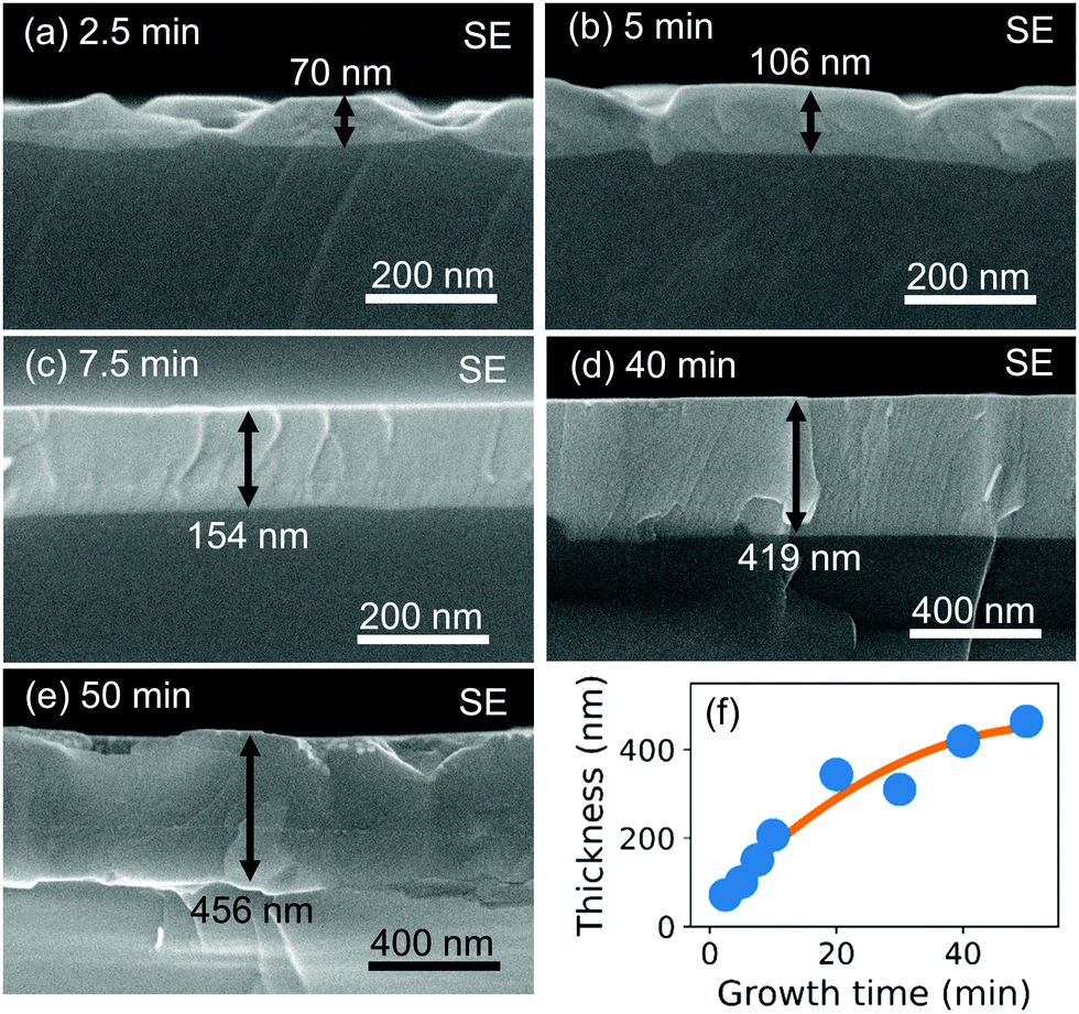 | ||
| Fig. 7 (a–e) Cross-sectional SEM images of the CSE films synthesized at 700 °C for 2.5–50 min using 60 s milled sources and (f) the trend of film thickness as a function of growth time. The orange line is a fitted quadratic function. | ||
Fig. 8 shows XRD patterns of the CSE films synthesized at 700 °C for 7.5–50 min. All peaks observed can be indexed by BaSi2. In particular, the films synthesized for 7.5 and 40 min show (100) epitaxial patterns similar to the films synthesized at 800 and 900 °C shown in Fig. 3. The spotty 2D pattern of the 40 min sample shown as an inset is the evidence of epitaxial growth. For a growth time shorter than 7.5 min, the films presumably contain polycrystalline grains, which is evidenced from the 2D pattern (ESI,† Fig. S7) and 1D pattern (Fig. 3) of the film synthesized at 700 °C for 5 min. Epitaxial growth after long annealing agrees with the increase in epitaxial grains by postannealing of evaporated BaSi2 films.26,29 This phenomenon can be understood from the low surface and interface energies of (100) oriented grains.26 The film synthesized for 50 min also contains polycrystalline grains, as found from the 1D and 2D patterns of Fig. 8. This is possibly because of extensive re-evaporation of Ba. During the initial 10 min of CSE, a 200 nm-thick film is synthesized. However, the film thickness increases only by 37 nm from 40 to 50 min. This slow film growth suggests most of the adsorbed Ba atoms re-evaporate. The rough surface [Fig. 7(e)] also suggests that the re-evaporation rate differs depending on the place due to the in-plain inhomogeneity, which means that BaSi2 decomposes to Ba gas and solid Si in some places. Thus the produced Si is presumably polycrystalline and can react with deposited Ba atoms to produce polycrystalline BaSi2 grains. This mechanism can explain the observed polycrystallization after long CSE growth.
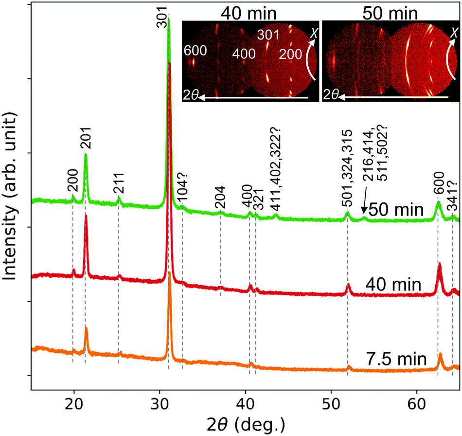 | ||
| Fig. 8 1D XRD patterns generated from 2D patterns of CSE films synthesized at 700 °C for 7.5–50 min. Insets display original 2D patterns for 40 and 50 min. | ||
The surface SEM images of the CSE films prepared at 700 °C are compared in Fig. 9. The films synthesized for 2.5–10 min were free from cracks. In particular, the 10 min sample appeared most flat. The root-mean-square roughness, measured by atomic force microscopy (VN8010, KEYENCE), in a 50 μm × 50 μm area on the surface was 5.3 nm, which is lower than those for evaporated films30,31 and sputtered films32 and is higher than that for MBE films.28,33 From 20 to 40 min, narrow lines appear on the surface like the film synthesized at 800 °C (Fig. 6). Also noticed are dark spots, which are the surface pits possibly formed by re-evaporation. After 50 min of CSE, the narrow lines and dark spots become more distinct than the shorter time. Dark spots match with the large pits observed in Fig. 7(e). The 400 and 600 XRD peaks of the film synthesized for 50 min are shifted to lower angles compared to the 7.5 and 40 min films (Fig. 8). These peak shifts indicate that the films synthesized for 40 min and shorter are tensile stressed while the 50 min film is relaxed by cracking. From the above observations, relatively flat and crack-free, epitaxial BaSi2 films can be prepared at 700 °C for the duration of 7.5–40 min, which corresponds to the thickness range of 150–419 nm.
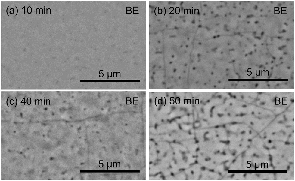 | ||
| Fig. 9 Surface SEM images of the CSE films synthesized at 700 °C for 10–50 min. | ||
Lastly, electrical and photoconductive properties were analyzed. Fig. 10 summarizes electron concentration and Hall mobility of the CSE samples synthesized at 700 °C determined by Hall effect measurements using the van der Pauw geometry. Although the film synthesized for 2.5 min is not a continuous film but consists of crystal islands formed on a p-type substrate, n-type conductivity and a high mobility were detected. This is understood by considering the conductivity inversion of the Si substrate surface. As depicted in Fig. 10, the conductivity of Si surface can change from p- to n-type in contact with BaSi2 due to a considerable difference in electron affinity.35,36 Even if the BaSi2 film is separated to crystal islands connected with a very thin film, current can flow through the induced n-type Si layer. A high electron mobility of 1.37 × 103 cm2 V−1 s−1 may also be owing to this current path.
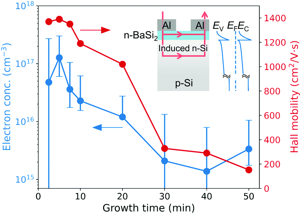 | ||
| Fig. 10 Electron concentration and average Hall mobility of the CSE samples synthesized at 700 °C as a function of growth time. The inset shows the schematic drawing of the current path during Hall effect measurements and the band alignment calculated by the wxAMPS software.34 Error bars denote the range of speculated electron concentration assuming three current paths. | ||
Similar Si conduction is expected for cracked or high-resistance films. When a film is thin and is of low carrier concentration, the depletion layer in BaSi2 extends to the surface, which further increases the film resistivity. Even if current flows solely through the BaSi2 film, the measured electron concentration can be underestimated. We therefore speculated the electron concentration excluding the effect of contact by considering three current paths: (1) through a depleted BaSi2 film, (2) through an induced n-type Si layer, and (3) through both the BaSi2 and Si layers. We calculated average electron concentration through assumed current paths using the band alignment simulated by the wxAMPS software,34 which numerically solves the Poisson equation. Free carrier densities were computed by n = NCF1/2![[thin space (1/6-em)]](https://www.rsc.org/images/entities/char_2009.gif) exp(EF − EC)/kT and p = NVF1/2exp(EV − EF)/kT, where NC and NV are the effective densities of states of the conduction and the valence bands, respectively, F1/2 is the Fermi integral of order one half, EF is the Fermi level, EC is the conduction band minimum, EV is the valence band maximum, k is the Boltzmann constant, and T is temperature (300 K). The thickness of the Si layer was assumed to be 10 μm, which is sufficiently thicker than the depletion layer thickness. The simulation was performed with a given electron concentration of BaSi2. The given electron concentration was optimized by trial and error so that the average electron concentration through the assumed current path can coincide with the experimental results.
exp(EF − EC)/kT and p = NVF1/2exp(EV − EF)/kT, where NC and NV are the effective densities of states of the conduction and the valence bands, respectively, F1/2 is the Fermi integral of order one half, EF is the Fermi level, EC is the conduction band minimum, EV is the valence band maximum, k is the Boltzmann constant, and T is temperature (300 K). The thickness of the Si layer was assumed to be 10 μm, which is sufficiently thicker than the depletion layer thickness. The simulation was performed with a given electron concentration of BaSi2. The given electron concentration was optimized by trial and error so that the average electron concentration through the assumed current path can coincide with the experimental results.
The speculated electron concentration is displayed in Fig. 10 as error bars. When current flows through the multiple layers, the experimental Hall mobility denotes the averaged value. Although the lower limits were not decided by this method for 2.5, 30, and 40 min, the upper limits were obtained for all samples. Clearly, electron concentration decreases as growth time increases. This decreasing trend possibly means the decrease in point defects caused by composition deviation. According to the first-principles defect calculation,37 the most probable point defects in BaSi2 are Si vacancies, which can act as electron donors. Decrease in electron concentration by heat treatment or by reducing composition deviation was previously observed in BaSi2 films prepared by thermal evaporation and MBE.38–40 These results indicate that the flat BaSi2 films fabricated by CSE (7.5–40 min) have a low electron concentration below 1.1 × 1017 cm−3, which is low enough for controlling the conductivity by impurity doping.
Hall mobility also decreases with growth time. Because the mobility in Si is presumably invariant, the change in mobility may reflect the transition of the current path from Si to BaSi2, which can occur when the film resistance decreases as film thickness increases with growth time. The decreasing mobility may result from the change in crystalline quality of the BaSi2 film. For example, the domain-separating lines and pits appearing on the BaSi2 surfaces after long CSE may account for the mobility degradation.
We further analyzed the photoconductance of the CSE BaSi2 films. Using Al contacts for Hall effect measurements, the effect of optical irradiation on the current–voltage characteristics were measured. Fig. 11(a) shows the current–voltage characteristics through the Al contacts on the BaSi2 film synthesized at 700 °C for 40 min. Linear characteristics confirm the ohmic contacts between Al and BaSi2. Under AM1.5 irradiation, current obviously increases, which is accounted for by photo-induced current increase. All the samples exhibited a photoresponse, which indicates that photoconductive BaSi2 films can be synthesized by CSE.
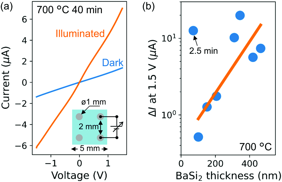 | ||
| Fig. 11 (a) Current–voltage characteristics through the surface Al contacts under dark and AM1.5 irradiation of the CSE sample prepared at 700 °C for 40 min. (b) Photo-induced current increase (ΔI) at 1.5 V as a function of BaSi2 film thickness. The orange line is a least-squares regression curve to the data for 5–50 min. | ||
Fig. 11(b) shows photo-induced current increase (ΔI) at 1.5 V as a function of BaSi2 film thickness. Except the thinnest film (2.5 min), ΔI tends to increase as films become thick. Because the Si substrate is not fully covered by BaSi2 after 2.5 min, a considerable proportion of incident light can reach the Si substrate and produce excess carriers. Due to the island morphology of BaSi2, current presumably flows through the Si substrate. Probably because the photo-excited carriers are generated on the current path (induced n-type Si layer), large ΔI is observed.
When the film thickness increases to 106 nm, ΔI drops to 1/25. This is presumably because the incident light reaching the Si substrate considerably decreases while the current flows mainly through the Si substrate. The absorption depth is below 106 nm for the wavelength below 682 nm in BaSi2. The irradiation photon flux below 682 nm amounts to 30% of total photon flux. Moreover, the absorption depth in Si exceeds 3 μm, which is the induced Si-layer thickness, for the wavelength longer than 630 nm. Thus, carrier generation decreases in the induced n-type Si layer by the increased absorption of low wavelength light in BaSi2 after a continuous film is formed. As BaSi2 thickness increases, optical absorption in BaSi2 further increases while the current path shifts to the BaSi2 layer. The increase in ΔI for over 100 nm thickness, therefore, indicates that photo-excited carriers in BaSi2 contribute to the observed photoconductance.
It is found that the thickest film yields large ΔI even though the film appears to be cracked [Fig. 9(d)]. This result suggests that cracks are narrow enough for current to pass through, or that there are some current paths that bridge neighboring domains. It should also be noted that ΔI does not necessarily correlate with BaSi2 thickness among the four thickest samples. This inconsistency could be attributed to the difference in crystalline quality of BaSi2. As found in SEM images (Fig. 9), pits and domain-separating lines are observed on thick films. After 50 min of CSE, the tensile stress in the film is relaxed probably due to these defects. The same photoconductance analysis on the p-type Si substrate yielded a ΔI of 275 μA, which is more than ten times larger compared to the CSE samples in this study. The quality of BaSi2 films should, hence, be improved. For improving the quality of the CSE BaSi2 films, the correlation between the defects and properties should be investigated in future studies. In particular, the domain-separating lines or cracks are owing to the mismatch of linear expansion coefficients between the BaSi2 film and the substrate, which can be further reduced by selecting a different material for the substrate. For cost-effective photovoltaic applications, glass substrate with a higher linear expansion coefficient than Si is worth investigating. BaSi2 would be synthesized on a pre-deposited Si layer as thermal evaporation of BaSi2 using Ba-rich vapor was similarly possible.41
4 Conclusions
Mechanochemical treatment of the BaAl4–Ni source enables lowering the BaSi2 film synthesis temperature in CSE. Vibratory ball milling of the optimum duration lowers the film synthesis temperature to 700 °C from 1000 °C owing to mechanical activation. Beyond the optimum milling time, Ba gas generation rate decreases presumably because of the Ni dissolution into BaAl4, which results in reduced driving force of Ba gas generation. Crack-free BaSi2 films are successfully synthesized at 700 °C when the thickness is 419 nm or below. Electron concentration in the films is lower than 1.1 × 1017 cm−3, which decreases with increasing growth time. Hall mobility also decreases with growth time probably because of macroscopic defects. All the crack-free BaSi2 samples clearly show photoconductance. Except the island-grown sample, the photo-induced current positively correlates with the BaSi2 thickness, clearly indicating the contribution of BaSi2. Mechanochemically assisted CSE thus opens the way for solar cell applications by realizing crack-free films and obvious photoconductance.Conflicts of interest
There are no conflicts to declare.Acknowledgements
This work was partly supported by JSPS KAKENHI Grant No. JP17K14657 and JP21K04136.References
- K. Yoshikawa, H. Kawasaki, W. Yoshida, T. Irie, K. Konishi, K. Nakano, T. Uto, D. Adachi, M. Kanematsu and H. Uzu, et al. , Nat. Energy, 2017, 2, 17032 Search PubMed.
- K. Toh, T. Saito and T. Suemasu, Jpn. J. Appl. Phys., 2011, 50, 068001 CrossRef.
- M. Kumar, N. Umezawa and M. Imai, Appl. Phys. Express, 2014, 7, 071203 CrossRef CAS.
- C. T. Trinh, Y. Nakagawa, K. O. Hara, R. Takabe, T. Suemasu and N. Usami, Mater. Res. Express, 2016, 3, 076204 CrossRef.
- W. Shockley and H. J. Queisser, J. Appl. Phys., 1961, 32, 510–519 CrossRef CAS.
- C. B. Honsberg and S. G. Bowden, Photovoltaics Education Website, www.pveducation.org.
- K. O. Hara, N. Usami, K. Nakamura, R. Takabe, M. Baba, K. Toko and T. Suemasu, Appl. Phys. Express, 2013, 6, 112302 Search PubMed.
- N. M. Shaalan, K. O. Hara, C. T. Trinh, Y. Nakagawa and N. Usami, Mater. Sci. Semicond. Process., 2018, 76, 37–41 CrossRef CAS.
- M. Baba, K. Toh, K. Toko, N. Saito, N. Yoshizawa, K. Jiptner, T. Sekiguchi, K. O. Hara, N. Usami and T. Suemasu, J. Cryst. Growth, 2012, 348, 75–79 CrossRef CAS.
- T. Suemasu and N. Usami, J. Phys. D: Appl. Phys., 2016, 50, 023001 CrossRef.
- K. Kodama, Y. Yamashita, T. Kaoru and T. Suemasu, Appl. Phys. Express, 2019, 12, 041005 CrossRef CAS.
- S. Yachi, R. Takabe, K. Toko and T. Suemasu, Jpn. J. Appl. Phys., 2017, 56, 05DB03 CrossRef.
- K. O. Hara, S. Takizawa, J. Yamanaka, N. Usami and K. Arimoto, Mater. Sci. Semicond. Process., 2020, 113, 105044 CrossRef CAS.
- T. A. Giorgi, Jpn. J. Appl. Phys., 1974, 13, 53 CrossRef.
- J. C. Turnbull, J. Vac. Sci. Technol., 1977, 14, 636–639 CrossRef CAS.
- K. O. Hara, S. Kunieda, J. Yamanaka, K. Arimoto, M. Itoh and M. Kurosawa, Mater. Sci. Semicond. Process., 2021, 132, 105928 Search PubMed.
- P. Baláž, M. Achimovičová, M. Baláž, P. Billik, Z. Cherkezova-Zheleva, J. M. Criado, F. Delogu, E. Dutková, E. Gaffet and F. J. Gotor, et al. , Chem. Soc. Rev., 2013, 42, 7571–7637 RSC.
- C. Suryanarayana, Prog. Mater. Sci., 2001, 46, 1–184 Search PubMed.
- T. Friščić, C. Mottillo and H. M. Titi, Angew. Chem., Int. Ed., 2020, 59, 1018–1029 Search PubMed.
- L. Takacs, Prog. Mater. Sci., 2002, 47, 355–414 Search PubMed.
- L. B. Kong, T. Zhang, J. Ma and F. Boey, Prog. Mater. Sci., 2008, 53, 207–322 Search PubMed.
- T. Goebel, Y. Prots and F. Haarmann, Z. Kristallogr. – New Cryst. Struct., 2009, 224, 7–8 Search PubMed.
- K. Toh, K. O. Hara, N. Usami, N. Saito, N. Yoshizawa, K. Toko and T. Suemasu, J. Cryst. Growth, 2012, 345, 16–21 Search PubMed.
- K. Toh, K. O. Hara, N. Usami, N. Saito, N. Yoshizawa, K. Toko and T. Suemasu, Jpn. J. Appl. Phys., 2012, 51, 095501 Search PubMed.
- K. O. Hara, C. T. Trinh, Y. Nakagawa, Y. Kurokawa, K. Arimoto, J. Yamanaka, K. Nakagawa and N. Usami, JJAP Conf. Proc., 2017, 5, 011202 Search PubMed.
- K. O. Hara, C. Yamamoto, J. Yamanaka, K. Arimoto, K. Nakagawa and N. Usami, Mater. Sci. Semicond. Process., 2017, 72, 93–98 Search PubMed.
- K. O. Hara, N. Usami, K. Nakamura, R. Takabe, M. Baba, K. Toko and T. Suemasu, Phys. Status Solidi C, 2013, 10, 1677–1680 Search PubMed.
- Y. Inomata, T. Nakamura, T. Suemasu and F. Hasegawa, Jpn, J. Appl. Phys., 2004, 43, L478–L481 Search PubMed.
- K. O. Hara, C. T. Trinh, Y. Kurokawa, K. Arimoto, J. Yamanaka, K. Nakagawa and N. Usami, Jpn. J. Appl. Phys., 2017, 56, 04CS07 Search PubMed.
- Y. Nakagawa, K. O. Hara, T. Suemasu and N. Usami, Jpn. J. Appl. Phys., 2015, 54, 08KC03 Search PubMed.
- Y. Kimura, K. Gotoh, Y. Kurokawa and N. Usami, Appl. Phys. Express, 2020, 13, 051002 Search PubMed.
- Y. Tian, M. Zeman and O. Isabella, Phys. Rev. Mater., 2020, 4, 125403 Search PubMed.
- M. Baba, K. Nakamura, W. Du, M. A. Khan, S. Koike, K. Toko, N. Usami, N. Saito, N. Yoshizawa and T. Suemasu, Jpn. J. Appl. Phys., 2012, 51, 098003 Search PubMed.
- Y. Liu, Y. Sun and A. Rockett, Sol. Energy Mater. Sol. Cells, 2012, 98, 124–128 Search PubMed.
- T. Suemasu, K. Morita, M. Kobayashi, M. Saida and M. Sasaki, Jpn. J. Appl. Phys., 2006, 45, L519–L521 Search PubMed.
- W. Du, M. Baba, K. Toko, K. O. Hara, K. Watanabe, T. Sekiguchi, N. Usami and T. Suemasu, J. Appl. Phys., 2014, 115, 223701 Search PubMed.
- M. Kumar, N. Umezawa, W. Zhou and M. Imai, J. Mater. Chem. A, 2017, 5, 25293–25302 Search PubMed.
- T. Suhara, K. Murata, A. Navabi, K. O. Hara, Y. Nakagawa, C. T. Trinh, Y. Kurokawa, T. Suemasu, K. L. Wang and N. Usami, Jpn. J. Appl. Phys., 2017, 56, 05DB05 Search PubMed.
- K. O. Hara, K. Arimoto, J. Yamanaka and K. Nakagawa, J. Mater. Res., 2018, 33, 2297–2305 Search PubMed.
- R. Takabe, T. Deng, K. Kodama, Y. Yamashita, T. Sato, K. Toko and T. Suemasu, J. Appl. Phys., 2018, 123, 045703 Search PubMed.
- K. O. Hara, J. Yamanaka, K. Arimoto, K. Nakagawa, T. Suemasu and N. Usami, Thin Solid Films, 2015, 595A, 68–72 Search PubMed.
Footnote |
| † Electronic supplementary information (ESI) available: Supplementary experimental data including SEM-EDX mapping, cross-sectional SEM, and XRD results. See DOI: 10.1039/d1ma00687h |
| This journal is © The Royal Society of Chemistry 2021 |