
 Open Access Article
 This Open Access Article is licensed under a Creative Commons Attribution-Non Commercial 3.0 Unported Licence
Fast non-ambipolar diffusion of charge carriers and the impact of traps and hot carriers on it in CsMAFA perovskite and GaAs†
Hannu P.
Pasanen
 *a,
Maning
Liu
a,
Hermann
Kahle
b,
Paola
Vivo
a and
Nikolai V.
Tkachenko
*a
*a,
Maning
Liu
a,
Hermann
Kahle
b,
Paola
Vivo
a and
Nikolai V.
Tkachenko
*a
aChemistry and Advanced Materials Group, Faculty of Engineering and Natural Sciences, Tampere University, Korkeakoulunkatu 8, FI-33720 Tampere, Finland. E-mail: hannu.pasanen@tuni.fi; nikolai.tkachenko@tuni.fi
bOptoelectronics Research Centre (ORC), Physics Unit/Photonics, Faculty of Engineering and Natural Sciences, Tampere University, Korkeakoulunkatu 3, FI-33720 Tampere, Finland
First published on 14th September 2021
Abstract
We performed a comprehensive study of the charge carrier diffusion in the CsMAFA perovskite, one of the state-of-the-art perovskites for photovoltaic applications, starting from the diffusion of hot carriers to the eventual trapping at the surfaces and grain boundaries. We discovered evidence of non-ambipolar diffusion by using ultrafast transient reflectance spectroscopy: by comparing the transient reflectance signals of perovskite samples to a GaAs reference sample, we saw that the electrons diffused at their maximum mobility without being hindered by the slower holes. These findings dispute the common assumption of ambipolar diffusion in these materials. Then, after a few tens of picoseconds, the diffusion decelerated from 1.6 cm2 s−1 to 0.2 cm2 s−1 due to traps and grain boundaries. The hot-carrier dynamics of perovskites have also garnered great interest thanks to their reported quasi-ballistic mobility and the slow cooling caused by the hot-phonon bottleneck. However, our findings dispute the ultrafast diffusion and provide an alternative explanation for the prolonged cooling. Based on our analysis, we recommend paying great attention to the carrier distribution when conducting hot-carrier studies.
1 Introduction
When it comes to the diffusion of charge carriers in metal halide perovskites, a number of questions remain, such as (1) to what extent the grain boundaries,1–3 traps4,5 and other defects limit the diffusion in solar cells compared to the ideal single crystals and (2) do hot carriers truly diffuse at quasi-ballistic speeds as suggested by some authors.6–9 To answer these questions we deployed transient reflectance (TR) which allows monitoring the carrier distribution inside the perovskite film perpendicularly to the film surface. The carrier mobility determined this way is much more relevant for solar cells and other applications: the common contact-free carrier diffusion measurement techniques are limited to monitoring the diffusion in micrometer scale across multiple grain boundaries10,11 or the short-distance sum mobility of electrons and holes,12,13 which can be two orders of magnitude apart14 and do not reflect the real-life performance of the solar cells as accurately as the TR does.Our comprehensive diffusion study provides a detailed analysis of the carrier behaviour starting from the hot carriers in femtosecond range to the trapping of the charge carriers in pico- to nanosecond range in the (CsI)0.05[(MAPbBr3)0.15(FAPbI3)0.85]0.95 perovskite (CsMAFA), which has reached over 20% power conversion efficiency.15 The diffusion of hot carriers has been under debate after it was suggested to be extremely fast (quasi-ballistic) by groups who used ultrafast transient absorption to monitor the spread of the charge carriers parallel to the film surface.7,9 It has also been suggested that the so-called hot phonon bottleneck phenomenon extends the lifetime of these hot carriers: the hot electrons cool down by transferring energy to the lattice via longitudinal optical (LO) phonons, which themselves take longer to release the energy to the rest of the system, maintaining higher average carrier temperature as the phonons have the same temperature as the excited carriers.16–18 We show that the carriers are indeed initially fast and then decelerate as they hit traps and grain boundaries, as suggested by the trapping–detrapping model.4 However, instead of the ultrafast hot carriers and the hot phonon bottleneck, we provide alternative explanations for the fast diffusion and the slow cooling of the hot carriers. We validated our transient reflectance model and results by also looking at GaAs wafers and thin films, which shared interesting similarities to our perovskite results and hinted that the carrier diffusion in these materials might not be ambipolar as has been commonly assumed. We also report various important side results, such as a TR signal that originates from unreacted lead iodide (PbI2) and the impact of surface traps in GaAs.
2 Measurements and modelling
2.1 TR model
Transient reflectance (TR) is technique similar to the commonly used transient absorption (TA), the only difference being that the former measures change in reflected light and latter the change in transmitted light. TR is more sensitive to the carrier distribution than TA, which is why it can be utilized to study the diffusion of charge carriers. There have been two models for analyzing TR signals:1. the surface carrier concentration (SCC) model, which assumes that the TR signal strength directly correlates with the charge carrier concentration at the sample surface,19–21 and
2. the thin-film interference (TFI) model, which calculates the interference generated by a non-uniform carrier distribution not only at the two interfaces (air–film and film–substrate) but also factors in the gradual shift in the refractive index inside the film.22
The TFI model can be used universally in many different situations, but it is more complex to use, whereas the SCC model is a simplified approximation and only accurate under certain circumstances. For our diffusion analysis, we picked some measurement wavelengths where both of these models are in good agreement with each other, but for example the perovskite NIR measurements could only be analysed with the TFI model. Whether or not the SCC can be used depends on the opacity of the sample and the photoinduced changes in the refractive index (Δn) and the extinction coefficient (Δk), which is related to the absorption coefficient. We have included one example in the ESI† (Fig. S5) where the film is opaque but the SCC model fails to reproduce the signal because of an inconvenient Δn/Δk ratio at that measurement wavelength.
Our TFI based TR model has been published in our previous articles,22,23 and we describe it in more detail in the ESI.† In short, the steps required for the TFI model are
1. Estimate the thickness and the complex refractive index of the sample either from steady state measurements or the literature.
2. Measure the TR and TA signals of the sample by using an excitation wavelength close to the bandgap in order to have as homogeneous carrier distribution as possible.
3. Calculate the Δn and Δk from the TR and TA with uniform carrier distribution.
4. Estimate any other relevant factors such as recombination rates.
5. Measure the TR and TA signals again but using short excitation wavelength to produce an inhomogeneous carrier distribution.
6. Fit the diffusion coefficient by modelling the TR signal based on the Δn and Δk.
2.2 Measurements
Our perovskite samples were so-called CsMAFA perovskite ((CsI)0.05[(MAPbBr3)0.15(FAPbI3)0.85]0.95). We used four sample types for this study:1. 70 nm CsMAFA perovskite films with and without electron or hole transport layer (ETL or HTL).
2. Approximately 500 nm CsMAFA perovskite films.
3. A 500 nm GaAs thin film coated with a thin 20 nm layer of GaInP.
4. A GaAs wafer typically used for epitaxial growth.
The 70 nm perovskite films were used for two purposes: First we established that the transient reflectance and absorption signals of perovskite originate from the photoexcited electrons while the holes have little impact on the signal (Fig. S7, ESI†). Secondly, the pristine 70 nm was also used for fitting the Δn and Δk at 430–600 nm wavelengths (Fig. S6(a), ESI†) where the absorption coefficient is too high for the transient transmittance signal to penetrate a standard 500 nm CsMAFA perovskite film. As mentioned in the previous section, the Δn/Δk information was necessary for modelling the diffusion in the 500 nm thick perovskite films. The measurements performed on these 70 nm perovskite films and their results are only shown in the ESI,† as they were only a preliminary step for the diffusion modelling. It was also determined that the 430–600 nm TA and TR spectra were not significantly impacted by the carrier temperature or other relaxation processes.
The GaAs thin film was similarly used for fitting the Δn and Δk (Fig. S11, ESI†) because it is not possible to measure transmittance from a GaAs wafer. Unlike the 500 nm perovskite film, the GaAs film could not be used for the determination of the diffusion constant because of a competing relaxation process during the first 10 ps (more on this in the results section).
Once we had the Δn and Δk necessary for the modelling, the carrier diffusion was measured from the 500 nm perovskite films and the GaAs wafer using transient reflectance. For the perovskite, we focused on using either 430–550 nm wavelengths in the visible range or 1000–1200 nm wavelengths in the NIR for the diffusion fitting. Although we were able to reproduce the general behaviour of the TR signal in the entire wavelength range from 430 nm to 1200 nm, the TR signal near the bandgap (650–850 nm) was omitted from the diffusion analysis because the bandgap normalization and other effects impacted the TR, complicating the fitting process for accurate results. Similarly to the perovskite, the GaAs wafer diffusion measurements were carried out at 1000–1200 nm wavelengths. The excitation wavelength ranged from 400 nm to 825 nm depending on the measurement and the sample, and the pump power was also varied in order to analyse the carrier recombination rates and the hot carrier behaviour.
2.3 Diffusion model
The diffusion equation is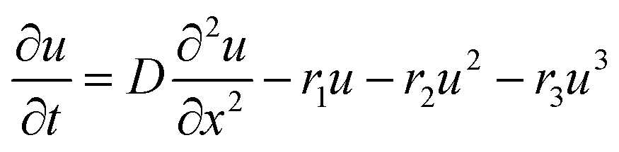 | (1) |
| CsMAFA air–film | CsMAFA film–substrate | GaAs air–wafer | GaAs wafer at 9 μm |
|---|---|---|---|
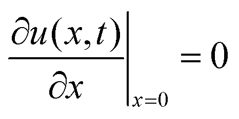
|
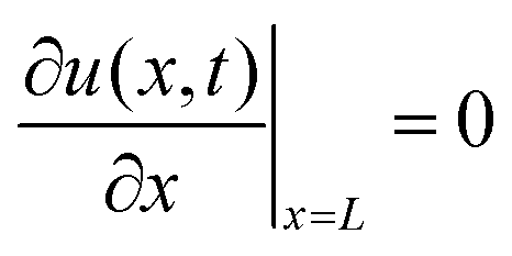
|
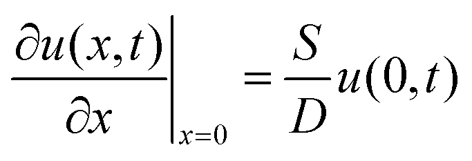
|
u(L,t) = 0 |
In the case of perovskite, the diffusion constant was found to decrease after tens of picoseconds. We therefore used equation
| D = D0 + D1e−t/τ | (2) |
3 Results and discussion
3.1 Hot carrier relaxation and oversaturation in CsMAFA perovskite
Before we analysed the charge carrier diffusion, we focused on the lifetime and TA behaviour of the hot carriers. We found that with high pump power, the electrons remained at an elevated energy level up to nanoseconds long after the initial cooling of hot carriers within the 1st picosecond. This was evident from the slight blueshift of the bandgap, which then slowly redshifted until the bandgap bleaching matched the lower power measurements, as shown in Fig. 1(a and b). The blueshift depended on pump power and wavelength, increasing with higher pump power and shorter excitation wavelength. The slow cooling phenomenon could be related to the so-called “hot phonon bottleneck” often discussed in literature.17 Alternatively, this could simply be caused by oversaturation and band-edge filling,24 meaning that with high carrier concentration the lowest conduction band is completely occupied and some of the carriers can only relax to the higher levels in the conduction band. In the case of short excitation wavelength the carriers are mostly generated at the surface (absorption coefficient of the sample is high), causing the local carrier concentration to be very high and oversaturate the film surface. The blueshift then disappears as the carrier concentration drops due to diffusion and recombination. | ||
| Fig. 1 Normalized TA response of a perovskite film with 400 nm excitation as a function of pump energy. (a) Solid lines represent the signal at 2 ps and the dashed lines at 1 ns delay time, showing that the bandgap bleaching is initially blueshifted with high pump energy. (b) TA response at 705 nm, normalized based on bandgap bleaching at 2 ps. We also measured TR to ensure that any photoinduced changes in reflectance are not causing these changes in transmittance. | ||
Let us take a look at, for example, the excitation at 400 nm with 7.7 μJ cm−2 energy and how much it saturates the bandgap. CsMAFA has a very high absorbance at 400 nm, approximately 6 for a 500 nm film, and thus majority of the carriers are generated at the perovskite surface within 50 nm. In this measurement, the bandgap bleaching at 750 nm probe wavelength was −50 mOD at 1 ps delay time (see Fig. S4, ESI†). However, a 50 nm thick perovskite layer only has a steady-state absorbance of approximately 50 mOD at 750 nm wavelength in the first place. Therefore, after the excitation, the lowest conduction band of the 50 nm thick surface layer is almost fully saturated and the carriers have no room to fully relax after the initial cooling. Further cooling (reduction in the blueshift of the TA signal) then occurs as the carriers diffuse and recombine, reducing the carrier concentration at the surface.
Nonetheless, even these elevated energy levels up to nanoseconds failed to increase diffusion speed in any relevant fashion, as is shown below in the diffusion fitting results.
3.2 Carrier diffusion and trapping in CsMAFA perovskite
We performed the diffusion analysis using two different measurement wavelength ranges: visible range (450–600 nm) and the NIR (1000–1200 nm). An example of the visible range measurement and data fitting is given in Fig. 2 which presents (a) the modelled carrier distribution over time and (b) the comparison between the simulated and the measured TR at 477 nm with 400 nm excitation. Examples of the NIR results are given in Fig. 3 where the same sample was pumped with excitation wavelengths ranging from 400 to 730 nm. All the diffusion fitting results are summarized in Table 2, and see Table S1 (ESI†) for all the fitting settings. Most of the measurements were performed in the NIR because the 450–600 nm TR spectra varied from sample to sample, as shown in Fig. 4(a). We assigned these differences to the amount of unreacted PbI2 at the sample surface because PbI2 has its bandgap close to 500 nm.25 This PbI2 signal disappeared very quickly (Fig. 4(b)), suggesting either fast recombination or charge transfer within few picosecond time-scale. The PbI2 signal was at its strongest from the film–substrate interface, revealing that the majority of the unreacted PbI2 is located there. The PbI2 signal was not significant at wavelengths longer than 600 nm, and therefore the NIR measurements were not impacted by this problem. The NIR measurements are also generally less surface-sensitive than the visible range measurements. Only the sample 2 in Table 2 was selected for the visible range diffusion fit thanks to its lowest PbI2 response. | ||
| Fig. 2 Visible range TR data of a perovskite sample (P2 in Table 2, 400 nm excitation) compared to diffusion fit with D = (0.20 + 1.40e−t/40ps) cm2 s−1: (a) carrier distribution over time, (b) TR signal compared to the TR simulation at 477 nm wavelength. The figure shows both our interference based model (sim. ΔR) and the commonly used carrier concentration at the surface (sim. scc, averaged over 18 nm). | ||
 | ||
| Fig. 3 The influence of the pump wavelength on the perovskite NIR TR signal: (a) TR signals at 5 ns delay time at 1000–1200 nm wavelengths, normalized to 1 at 1070 nm. (b) TR signals from 1 ps to 5 ns at 1124 nm, solid lines are the measured data and dashed lines are the diffusion fits with D = (0.20 + 1.20·e−t/60ps) cm2 s−1. | ||
| Sample | Measurement | Pump (nm) | Energy (μJ cm−2) | D 0 (cm2 s−1) | D 1 | τ (ps) |
|---|---|---|---|---|---|---|
| P1 | NIR | 400 | 1.4 | 0.20 | 1.20 | 40 |
| 400 | 4.6 | 0.20 | 1.20 | 40 | ||
| P2 | vis | 400 | 7.7 | 0.20 | 1.40 | 40 |
| P3 | NIR | 510 | 1.5 | 0.20 | 1.30 | 60 |
| 510 | 3.5 | 0.20 | 1.30 | 60 | ||
| 510 | 6.5 | 0.20 | 1.40 | 80 | ||
| P4 | NIR | 600 | 1 | 0.20 | 1.40 | 80 |
| 600 | 2.3 | 0.20 | 1.40 | 80 | ||
| 600 | 5.3 | 0.20 | 1.40 | 80 | ||
| P5 | NIR | 700 | 2 | 0.20 | 1.60 | 80 |
| 700 | 4 | 0.20 | 1.60 | 80 | ||
| 700 | 8 | 0.20 | 1.60 | 80 | ||
| P6 | NIR | 400–730 | 1.7 | 0.20 | 1.20 | 60 |
| GaAs wafer | NIR | 825 | 30 | 120 | 0 | 0 |
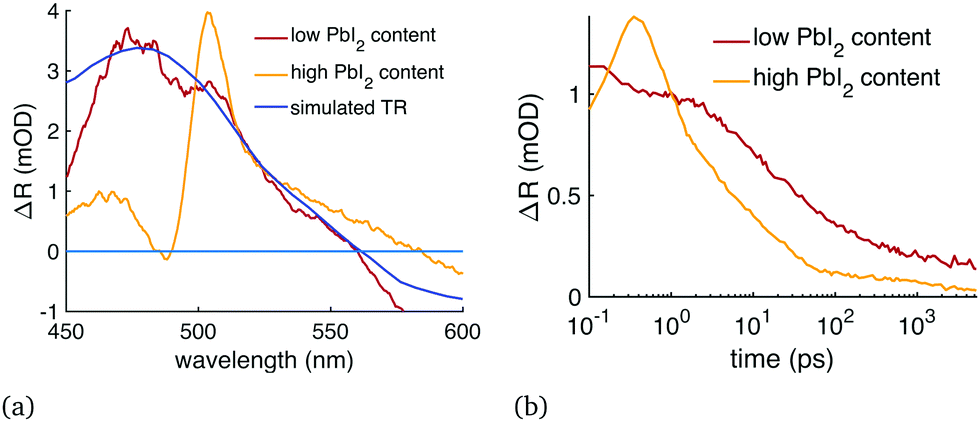 | ||
| Fig. 4 TR signal from unreacted PbI2. (a) TR spectra of CsMAFA perovskite samples with a high or low amount of unreacted PbI2 compared to the simulated TR at 450–600 nm wavelength range and 2 ps delay time, and (b) the evolution of these TR signals over time at 503 nm. Both figures were normalized to 1 at 503 nm and 1 ps delay time. The sample with a high amount of unreacted PbI2 has a sharp TR peak at 505 nm, while a pure perovskite has a TR peak at 475 nm, and unreacted PbI2 content of the samples could be assessed by comparing the relative strengths of these two peaks. | ||
The immediate finding was that the diffusion decelerates over time: the only way to reproduce the TR signal behaviour was to have initially fast diffusion for few tens of picoseconds, and then reduce the diffusion constant significantly. Due to this reduction in diffusion constant over time, we decided to use eqn (2) which has an exponential component (free diffusion of electrons) and a constant (electron diffusion across traps, defects and grain boundaries). This resulted in D = (0.20 + 1.40e−t/40ps) cm2 s−1 with some dependence on the excitation wavelength as shown in Table 2. This reduction of the diffusion constant over time was clear in both the NIR and visible range measurements, in other words our measurements and model matched across a very wide wavelength range. Secondly, Fig. 2(b) shows that under correct circumstances the two TR models, the SCC model used in the literature and our TFI model, both produce the same signal after 1 ps. Our initial diffusion of 1.6 cm2 s−1 matches many single-crystal results10 and terahertz sum mobility measurements14,22 while the 0.2 cm2 s−1 is more in line with other polycrystalline film measurements.3
Some of the carriers seemed to remain stuck near the surface up to 5 ns in Fig. 2(b), which is the limit of our instrument. The TR signal at 430–600 nm probe wavelengths was not reduced as fast as the bandgap bleaching was, although the recombination was relatively fast in the nanosecond scale due to high pump power and carrier density (sample P2 in Table 2). These results were supported by similar findings in the NIR measurements (Fig. 3(a and b)). In the NIR the assumed charge trapping manifested as an elevated TR signal of 400 and 510 nm excitations compared to 600 and 730 nm at measurement wavelengths 1130–1200 nm, in other words the TR signal of 400 nm excitation never relaxed to the same carrier distribution as the 730 nm excitation. Because the carrier trapping only occurs with pump wavelengths close to or below 500 nm when measuring in NIR, it could be connected to the unreacted PbI2 or other precursors that are excited with these pump wavelengths, or it could be simply due to the much higher initial carrier concentration at the surface, leaving a greater proportion of the carriers trapped. This also explains why the diffusion is reduced with shorter excitation wavelength. Judging by the strength of the measured signal at 5 ns delay time compared to the simulation, the sample surface has approximately twice as high carrier concentration as the bulk of the film. These carriers also have slower 2nd and 3rd order recombination rates, as expected if they are trapped and cannot reach each other.
The pump power either had no effect on diffusion or it only slightly increased the exponential part of the diffusion constant, despite the long-lasting blueshift of the bandgap bleaching with high pump power (Fig. 1). As mentioned previously, using shorter excitation wavelength did not increase diffusion either. Therefore, we found no evidence that the hot carriers diffuse any faster than cooled down carriers, but one could mistake the relaxation of PbI2 in Fig. 4(b) for very fast diffusion. Fig. S3 (ESI†) shows how the increase in pump power affects the recombination rate and the TR signal: the higher pump power increases the 2nd and 3rd order recombination, which hastens the formation of a uniform carrier distribution while the diffusion itself is mostly unaffected. Underestimating the 2nd and 3rd order recombination rates would thus lead to an overestimation of the diffusion constant, which perhaps explains the slightly faster diffusion with high pump power.
 | ||
| Fig. 5 (a) GaAs thin film NIR TA spectra with 700 nm pump. (b) GaAs wafer NIR TR spectra with 500 nm pump. Both of these spectra show slow carrier relaxation to the lowest conduction band at least up to 7 ps. | ||
Based on these findings, we decided to use 825 nm excitation for the GaAs charge carrier diffusion analysis. Any excitation wavelength higher than this would make the results unreliable: the relaxation to the lowest conduction band increases the TR signal strength while the diffusion reduces it, resulting in two competing processes.
The GaAs diffusion analysis was performed on the wafer sample TR data. These results shared many similarities to the perovskite results: after initially having very fast diffusion, which perfectly matches the diffusion constant of electrons in GaAs (120 cm2 s−1, Fig. 6), the TR showed clear signs of trapped charges contributing to the signal starting at 50–100 ps delay time. The carrier trapping caused the overall signal to shift from positive to negative. It is difficult to tell if the diffusion in GaAs slows down similarly to perovskites, because it could be overshadowed by the carrier trapping.
 | ||
| Fig. 6 TR data of the GaAs wafer compared to simulation with D = 120 cm2 s−1 similarly to Fig. 2: (a) carrier distribution over time, (b) TR signal compared to the TR simulation at 1060 nm wavelength. The figure shows both the TFI model (sim. ΔR) and the SCC model (sim. scc). Starting around 50–100 ps the measured ΔR deviates from the model and becomes negative at longer delay times presumably due to charge trapping at the surface. | ||
However, an interesting finding is that the modelled carrier diffusion in both GaAs and CsMAFA perovskite matches their presumed electron mobility. Hole mobility in GaAs is much slower than the electron mobility, causing the theoretical ambipolar diffusion to also be much slower than what we measured. Ambipolar diffusion has been the common assumption across most carrier diffusion studies and measurement techniques, including TR. In our previous study we deployed time-resolved terahertz spectroscopy (TRTS) to probe the sum mobility of both carrier types in the same perovskite,22 and the result of 65 cm2 (V s)−1 was very close to the initial mobility we measured here with TR: diffusion of 1.6 cm2 s−1 corresponds to mobility of 65 cm2 (V s)−1. The TRTS response is primarily determined by the faster carrier, unless both carrier types have approximately the same mobility, in which case TRTS would give a sum mobility twice as high as any ambipolar diffusion measurement would suggest. Because the measurement of the electron diffusion gave the same result as the sum mobility measurement, it implies that the diffusion is not ambipolar and that the electrons have higher mobility than the holes.
4 Conclusions
By using transient absorption and reflection techniques, we mapped the diffusion of photoinduced electrons in CsMAFA perovskite and GaAs. The primary findings and their specific timescales are listed in Table 3 for the perovskite and Table 4 for the GaAs. First we showed that the photoexcited charges in perovskite can remain at elevated energy levels up to nanoseconds if the carrier concentration is too high. However, instead of being caused by the hot-phonon bottleneck, we believe the slow cooling is caused by band-filling at the sample surface and recommend careful analysis of the carrier concentration and distribution when analyzing such phenomena with TA spectroscopy| 0–1 ps | Hot carrier relaxation unless oversaturated, D = 1.6 cm2 s−1. |
| 1–10 ps | Relaxation of PbI2 signal at the 500 nm wavelength. |
| 10–100 ps | Diffusion decelerates due to traps and grain boundaries, D = 0.2 cm2 s−1. |
| 1–5 ns | Uniform distribution except for the trapped carriers at the surface. |
| 0–7 ps | Carrier relaxation to the lowest conduction band, D = 120 cm2 s−1. |
| 50–300 ps | Carrier trapping at the surface. |
| >1 ns | TR signal originates primarily from the trapped carriers. |
However, our carrier diffusion measurements show that these elevated energy levels have little impact on the diffusion coefficient, giving no sign of the ultrafast hot-carrier diffusion reported by other groups. Instead, we found that the diffusion is non-ambipolar in both the perovskite and the GaAs, D ≈ 1.6 cm2 s−1 and 120 cm2 s−1, respectively. These findings question the very common assumption of ambipolar diffusion in perovskites and other semiconductors.
We also found strong evidence of charge trapping: in CsMAFA perovskite the initially fast diffusion (≈1.6 cm2 s−1) slows down to 0.2 cm2 s−1 within 100 ps, which hints of grain boundaries, traps and other defects slowing down the electron diffusion in the conduction band. The surface traps were present in both the perovskite and GaAs samples, and the TR signal of the latter was especially impacted by the traps. The carrier trapping at the surface occurred more with lower excitation wavelengths due to higher initial carrier concentration at the surface.
Finally, we also found a clear sample-to-sample variance in the perovskite TR signal near 500 nm that we attributed to unreacted PbI2, and that the majority of the unreacted PbI2 is located at the perovskite–substrate interface. These PbI2-induced TR features have potential use in perovskite quality assessment, as they allow a quick estimation of the amount of free PbI2 in the perovskite either due to incomplete synthesis or degradation.
Altogether, these findings provide a very comprehensive picture of the carrier diffusion in state-of-the-art perovskite thin films with greater accuracy than before. Additionally, the HC results presented here have direct implications for the research and development of HC devices, where the long-lasting cooling and ultrafast diffusion have been of great interest.
Author contributions
Hannu Pasanen: software, methodology, investigation, formal analysis, writing – original draft. Maning liu and Hermann Kahle: resources. Nikolai Tkachenko and Paola Vivo: supervision and writing – review & editing.Conflicts of interest
There are no conflicts to declare.Acknowledgements
The work is part of the Academy of Finland Flagship Programme, Photonics Research and Innovation (PREIN, 320165). Academy of Finland Postdoctoral Researcher funding for H. K. (326455) is acknowledged. M. L. thanks Finnish Cultural Foundation (00210670) for financial support. P. V. and H. P. P. thank Business Finland and Forschungszentrum Jülich GmbH (SolarWAVE project) and Jane & Aatos Erkko foundation (project ASPIRE) for financial support. H. P. P. also thanks the doctoral program of Tampere University for financial support. The authors thank Sanna Ranta from the Tampere University for the growth of the semiconductor thin film sample.Notes and references
- M. I. Saidaminov, K. Williams, M. Wei, A. Johnston, R. Quintero-Bermudez, M. Vafaie, J. M. Pina, A. H. Proppe, Y. Hou, G. Walters, S. O. Kelley, W. A. Tisdale and E. H. Sargent, Nat. Mater., 2020, 19, 412–418 CrossRef CAS PubMed.
- W. Li, S. K. Yadavalli, D. Lizarazo-Ferro, M. Chen, Y. Zhou, N. P. Padture and R. Zia, ACS Energy Lett., 2018, 3, 2669–2670 CrossRef CAS.
- J. M. Snaider, Z. Guo, T. Wang, M. Yang, L. Yuan, K. Zhu and L. Huang, ACS Energy Lett., 2018, 3, 1402–1408 CrossRef CAS.
- H. Jin, E. Debroye, M. Keshavarz, I. G. Scheblykin, M. B. J. Roeffaers, J. Hofkens and J. A. Steele, Mater. Horiz., 2020, 7, 397–410 RSC.
- A. Musiienko, J. Pipek, P. Praus, M. Brynza, E. Belas, B. Dryzhakov, M.-H. Du, M. Ahmadi and R. Grill, Sci. Adv., 2020, 6, eabb6393 CrossRef CAS PubMed.
- J. Sung, C. Schnedermann, L. Ni, A. Sadhanal, R. Y. S. Chen, C. Cho, L. Priest, J. M. Lim, H.-K. Kim, B. Monserrat, P. Kukura and A. Rao, Nat. Phys., 2020, 16, 171–176 Search PubMed.
- Z. Guo, Y. Wan, M. Yang, J. Snaider, K. Zhu and L. Huang, Science, 2017, 356, 59–62 CrossRef CAS PubMed.
- T. Wang, L. Jin, J. Hidalgo, W. Chu, J. M. Snaider, S. Deng, T. Zhu, O. P. Barry Lai, J.-P. Correa-Baena and L. Huang, Sci. Adv., 2020, 6, eabb1336 CAS.
- S. M. Jooyoung Sung and A. Rao, J. Phys. Chem. Lett., 2020, 11, 5402–5406 CrossRef PubMed.
- I. M. Hermes, A. Best, L. Winkelmann, J. Mars, S. M. Vorpahl, M. Mezger, L. Collins, H.-J. Butt, D. S. Ginger, K. Koynova and S. A. L. Weber, Energy Environ. Sci., 2020, 13, 4168–4177 RSC.
- A. Sridharan, N. K. Noel, H. Hwang, S. Hafezian, B. P. Rand and S. Kéna-Cohen, Phys. Rev. Mater., 2019, 3, 125403 CrossRef CAS.
- R. Ulbricht, E. Hendry, J. Shan, T. F. Heinz and M. Bonn, Rev. Mod. Phys., 2011, 83, 543–586 CrossRef CAS.
- D. H. Kim, J. Park, Z. Li, M. Yang, J.-S. Park, I. J. Park, J. Kim, J. J. Berry, G. Rumbles and K. Zhu, Adv. Mater., 2017, 29, 1606831 CrossRef PubMed.
- L. Herz, ACS Energy Lett., 2017, 2, 1539–1548 CrossRef CAS.
- M. Saliba, T. Matsui, J.-Y. Seo, K. Domanski, J.-P. Correa-Baena, M. K. Nazeeruddin, S. M. Zakeeruddin, W. Tress, A. Abate, A. Hagfeldtd and M. Grätzel, Energy Environ. Sci., 2016, 9, 1989–1997 RSC.
- M. Li, J. Fu, Q. Xu and T. C. Sum, Adv. Mater., 2019, 31, 1802486 CrossRef CAS PubMed.
- J. Yang, X. Wen, H. Xia, R. Sheng, Q. Ma, J. Kim, P. Tapping, T. Harada, T. W. Kee, F. Huang, Y.-B. Cheng, M. Green, A. Ho-Baillie, S. Huang, S. Shrestha, R. Patterson and G. Conibeer, Nat. Commun., 2017, 8, 14120 CrossRef CAS PubMed.
- H. Shi, X. Zhang, X. Sun and X. Zhang, Appl. Phys. Lett., 2020, 116, 151902 CrossRef CAS.
- Y. Yang, Y. Yan, M. Yang, S. Choi, K. Zhu, J. Luther and M. Beard, Nat. Commun., 2017, 6, 7961 CrossRef PubMed.
- Y. Yang, M. Yang, D. T. Moore, Y. Yan, E. M. Miller, K. Zhu and M. C. Beard, Nat. Energy, 2017, 2, 16207 CrossRef CAS.
- X. Chen, K. Wang and M. C. Beard, Phys. Chem. Chem. Phys., 2019, 21, 16399 RSC.
- H. P. Pasanen, P. Vivo, L. Canil, H. Hempel, T. Unold, A. Abate and N. V. Tkachenko, J. Phys. Chem. Lett., 2020, 11, 445–450 CrossRef CAS PubMed.
- H. P. Pasanen, P. Vivo, L. Canil, A. Abate and N. Tkachenko, Phys. Chem. Chem. Phys., 2019, 21, 14663–14670 RSC.
- J. S. Manser and P. V. Kamat, Nat. Photonics, 2014, 8, 737–743 CrossRef CAS.
- A. F. da Silva, N. Veissid and C. Y. An, Appl. Phys. Lett., 1996, 69, 1930–1932 CrossRef.
- A. D. Cicco, G. Polzoni, R. Gunnella, A. Trapananti, M. Minicucci, S. J. Rezvani, D. Catone, L. D. Mario, J. S. P. Cresi, S. Turchini and F. Martelli, Sci. Rep., 2020, 10, 17363 CrossRef PubMed.
Footnote |
| † Electronic supplementary information (ESI) available: TFI model details, workflow and Matlab codes, additional TA and TR data, 70 nm perovskite thin-film results, experimental details such as the pump–probe setup and sample fabrication. See DOI: 10.1039/d1ma00650a |
| This journal is © The Royal Society of Chemistry 2021 |