
 Open Access Article
 This Open Access Article is licensed under a
 Creative Commons Attribution 3.0 Unported Licence
CdS nanobelt-based self-powered flexible photodetectors with high photosensitivity†
Muhammad Zubair
Nawaz
 ,
Liu
Xu
,
Xin
Zhou
,
Khizar Hussain
Shah
,
Jiale
Wang
,
Binhe
Wu
and
Chunrui
Wang
*
,
Liu
Xu
,
Xin
Zhou
,
Khizar Hussain
Shah
,
Jiale
Wang
,
Binhe
Wu
and
Chunrui
Wang
*
College of Science and Shanghai Institute of Intelligent Electronics and Systems, Donghua University, 2999 Renmin Rd North, Songjiang District, Shanghai 201620, P. R. China. E-mail: crwang@dhu.edu.cn
First published on 6th August 2021
Abstract
Asymmetric contacts were used to assemble extremely photosensitive and self-powered photodetectors (SPDs) on rigid and polyimide (PI) substrates based on one-dimensional (1D)-CdS nanobelts. The photoresponse characteristics of the constructed devices were outstanding, including high photosensitivity (1.54 × 10⁶%), specific detectivity (2.36 × 10¹² Jones), responsivity (36 mA W−1) and noise equivalent power (2.94 × 10⁻¹⁵ W Hz−1/2) with 215 μW cm−2 light irradiation, as well as having high reproducibility, environmental stability and speedy response of less than 30 ms. Flexible self-powered photodetectors (FSPDs) were also constructed on PI substrates, which had comparable photoresponse performance to the rigid one. Additionally, the as-fabricated FSPDs showed excellent folding endurance, electrical and mechanical flexural stability. Our findings suggest that the asymmetric contact device design used in this study is appropriate for high-performance FSPDs, particularly ultrafast nanodevices.
Introduction
Flexible photodetectors have recently gained more attention due to their wide range of applications including motion detection, optical communications, sensing, biomedical imaging and missile warning.1,2 A key requirement in the optimal design of such flexible photodetectors is the power consumption. It is highly desired to develop FSPDs without external power input, which could remarkably enhance the adaptability and reduce the cost of the flexible photodetector.3–8 SPDs can be split into two categories.9 The first is constructed via the photovoltaic effect.10 The second is designed with integrated nanosystems that include an energy harvesting or storage unit as well as a light sensor.11 The maintenance-free features and simplified structure of the first category has a low-cost advantage over the second one.Due to their unique electrical and optoelectronic characteristics, metal chalcogenide semiconductors are interesting options for photoelectric devices.12 Cadmium sulfide (CdS) is a physiochemically interesting intermediate direct bandgap (2.4 eV) semiconductor with speedy response, low work function, high photosensitivity, large refractive index, and exceptional chemical and thermal stability. Therefore, it is a fascinating and potential candidate for self-powered photodetectors.13–23 For instance, Dai et al. reported FPSDs composed of p-Si/n-CdS nanowire heterostructures, which respond beyond the bandgap limitation with fast response speed at zero bias.24 Zhou et al. assembled ZnO nanoarray-GaN SPDs with a CdS inset layer, which exhibited high responsivity and specific detectivity.14 Although these SPDs exhibited enhanced photoresponse performance, the photosensitivity is relatively low, which significantly limits their practical applications in self-powered optoelectronic devices. Additionally, no research about FSPDs based on the pristine 1D-CdS nanostructure has been reported yet.20 We designed novel 1D-CdS nanobelt SPDs and FSPDs assembled by simple steps with excellent photoresponse properties, which can perform well in the broadband region at zero bias. The photogenerated carriers are separated speedily and efficiently because of the built-in electric field induced between the asymmetric interfaces. Notably, the device exhibited an ultra-low dark current of 36 fA, which consequently lead to a high photosensitivity of 1.54 × 10⁶%, high responsivity of 36 mA W−1, specific detectivity of 2.36 × 10¹² Jones, and noise equivalent power of 2.94 × 10⁻¹⁵ W Hz−1/2 under 215 μW cm−2 light irradiation. Moreover, the FSPDs demonstrated excellent folding endurance, electrical and mechanical flexural stability. The unique device design presented in this study might pave the way for improved FSPDs to be manufactured in the near future.
Experimental section
Material synthesis and characterization
The high-purity CdS nanobelts used in this study were obtained using a one-step vapor transport technique that was previously reported in detail.25,26 As a source material, 0.15 g of pure CdS powder (99.99%) was put on an alumina boat in the center of a tube furnace. To collect the product, Si substrates were drop coated with hydrated chloroauric acid (HAuCl4) dissolved in ethyl alcohol as the catalyst and placed on another alumina boat situated downstream, 8–11 cm from the tube center. The tube was pumped down to a base pressure of ∼2.5 × 10² Pa, which was kept the same during the experimental process. The tube was purged with pure argon gas for 1 hour, and then the system was heated to 800 °C and held there for 0.5–2 hours. The carrier gas flow rate was fixed at 50 sccm (standard cubic centimeters per minute). The furnace was naturally cooled to normal temperature when the process was completed. At room temperature, X-ray diffractometry (XRD, D/max-2550VB, λ = 1.5404 Å), laser micro-Raman spectroscopy (inVia-Reflex with a 532 nm He–Ne laser), field emission scanning electron microscopy (Hitachi FE-SEM S-4800) and field emission transmission electron microscopy (FE-TEM, JEM-2100F equipped with energy dispersive spectrometry (EDS)) were used to characterize the obtained samples.Photodetector fabrication and measurement
First, the Si and PI substrates were cleaned three times with ethanol and deionized water by ultrasonication for 1 hour. Next, the obtained suspension of ethanol and nanobelts was dispersed on SiO2/Si and PI substrates. Finally, unequal amounts of silver paste were deposited on both ends of the individual nanobelt to obtain asymmetric contacts and the device was dried at 70 °C for 3 hours. The optical measurements of both devices were taken on a Keithley-4200-SCS connected with a probe station at room temperature.Results and discussion
Characterization of CdS nanobelts
Fig. 1a shows the XRD patterns of the obtained CdS nanobelts. All of the detected peaks can be easily attributed to hexagonal wurtzite CdS with lattice parameters of a = 4.14 Å and c = 6.72 Å, in good agreement with JCPDS card No. 41-1049. Moreover, no additional characteristic impurity peaks are observed, showing that the resulting product is hexagonal wurtzite CdS.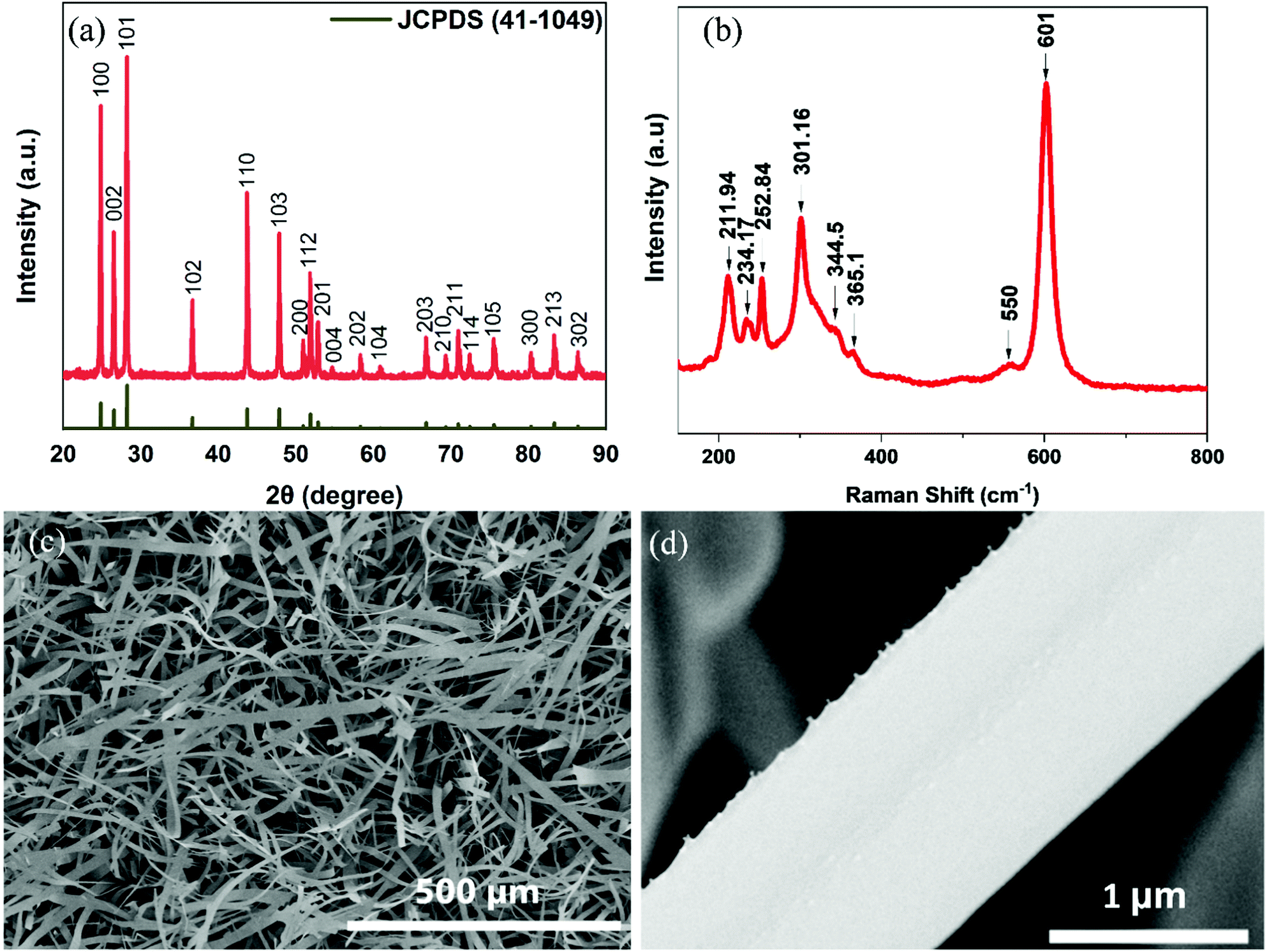 | ||
| Fig. 1 (a) XRD patterns. (b) Raman spectra of CdS nanobelts at room temperature. (c) FE-SEM of the obtained 1D-CdS nanobelts. (d) magnified view of a nanobelt. | ||
Fig. 1b shows the room temperature Raman spectra of the obtained CdS nanobelts. The hexagonal wurtzite CdS belongs to the C46v(p63mc) space group and may exhibit the lattice vibrational modes Γopt = A1 + 2B1 + E1 + 2E2. The A1, E1, and E2 (EH2 and EL2) are Raman active modes and B1 is inactive.27 The A1 and E1 modes are split into longitudinal optical (LO) and transverse optical (TO) components.28 The A1(TO) and EH2 are attributed to the two first order Raman peaks at 234 and 252.8 cm−1.29 The weak peaks at 211.9, 344.5, 365.0 and 550.0 cm−1 are attributed to multiphonon Raman scattering.30 The two strong peaks found at 301.0 and 601.0 cm−1 are identified as the first-order LO and second-order LO phonon modes of pure CdS, respectively. The assignment of all Raman scattering peaks is in good agreement with the literature.28–31 FE-SEM examination exhibited large scale and high density rectangle-shaped CdS nanobelts (Fig. 1c and d) that have a smooth surface with length ranging from 100–500 μm and uniform width of 2–40 μm.
A typical TEM picture of a single nanobelt is shown in Fig. 2a. The HRTEM image in Fig. 2b is obtained from the marked area depicting a lattice fringe separation of ∼0.335 nm and ∼0.316 nm, which agreed well with the (002) and (101) planes of hexagonal CdS, which further shows its single-crystalline nature, corresponding to the selected area electron diffraction (SAED) pattern (inset in Fig. 2b). The energy dispersive X-ray spectrum (EDS) shown in Fig. 2c reveals that the nanobelts consist of Cd and S elements, considering that the signal of Cu element is from the TEM grid. Fig. 2(d–f) illustrate the appropriate EDS elemental mapping, which supports the XRD pattern.
 | ||
| Fig. 2 (a) TEM. (b) HRTEM and SAED (inset) patterns. (c) EDS spectrum. (d–f) STEM and elemental mapping. | ||
Photoresponses of rigid and flexible CdS nanobelt photodetectors
Fig. 3a displays the schematic of a single CdS nanobelt photodetector. The light intensity dependence of the CdS nanobelt device was initially measured. The I–V plots of the CdS nanobelt device under 484 nm light are shown in Fig. 3b, with incoming light power rising from 10 to 215 μW cm−2. According to Fig. 3b, about 2 orders of magnitude change of photocurrent are demonstrated clearly. A remarkably enhanced photocurrent was gained when the light power density was increased from 10 to 215 μW cm−2. The device exhibited a photocurrent of 555 pA under 215 μW cm−2 using 484 nm light power. The photocurrent grows dramatically, which is owing to the charge carrier photogeneration efficiency improving as the absorbed photon flux increases. However, the dark current of the device was just 36 fA. Photosensitivity (Ps) is an important figure-of-merit to determine the capability of an optical detector, and defined by formula: Ps(%) = (Iph–Id)/Id × 100 where Iph and Id represent the photo- and dark current, respectively.32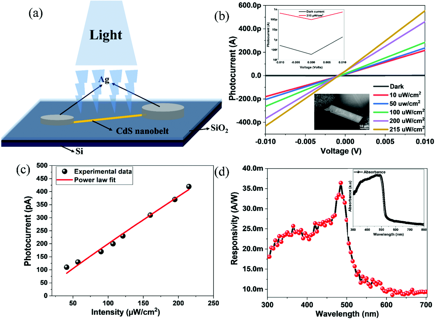 | ||
| Fig. 3 (a) Schematic illustration of SPD. (b) The I–V plots in the dark and at rising power densities (10–215 μW cm−2) under 484 nm illumination. Insets are the corresponding SEM image and semi-logarithmic I–V plot of SPDs, respectively. (c) Corresponding photocurrent reliance on light power density. The obtained fitting value of θ is 0.97 (I–P0.97). (d) Spectral response of the SPD. The corresponding absorbance spectra are shown in the inset. | ||
Fig. S1a (ESI†) shows that the Ps of our device was about 1.54 × 10⁶%, which is greater than those reported for 1D CdS nanodevices (see Table 1).6,20,33–38Table 1 further shows that the light intensity (215 W cm−2) utilized in our I–V test is less. Fig. 3c and Fig. S2a (ESI†) show the dependency of photocurrent on the power density at 0.01 V and 0 V, which can be articulated as power law, I = APθ, with the photocurrent I, the constant A, the light intensity P and the empirical value θ, which can be associated with the composite process of photoinduced carriers.39–42 The photocurrent and light intensity have a strong relationship, and fitting the experimental data yielded an exponential function of I–P0.97, which proved that the CdS nanobelts possess an amazing capability.
| Active material | Intensity of light | Optical wavelength | τ r/τd | Bias voltage | Photosensitivity | Ref. |
|---|---|---|---|---|---|---|
| CdS nanobelt | 10 W | White light | ∼1–3 s | — | <3000 | 33 |
| CdS nanorod | — | 400 nm | ∼2.3 s | 5 V | <40 | 34 |
| CdS thin film | 1.20 mW cm−2 | 500 nm | ∼9/10 ms | 0 V | 97.2 × 10³% | 20 |
| CdS nanowire | 16 mW cm−2 | 405 nm | ∼260 ms | 0.05 V | 30 | 35 |
| CdS nanowire | — | 490 nm | ∼150/53 ms | 1 V | 238% | 36 |
| CdS thin film | 1.20 mW cm−2 | 500 nm | ∼9/11 ms | 1 V | 5400% | 37 |
| CdS microrod | 10 mW cm−2 | 460 nm | ∼32/38 ms | 3 V | 0.82 × 10³% | 38 |
| CdS nanoribbon | 1.80 mW cm−2 | 490 nm | ∼0.74/0.79 ms | 1 V | 100% | 6 |
| CdS nanobelt (flexible) | 215 μW cm−2 | 484 nm | ∼80/50 ms | 0 V | >2.2 × 10³% | This work |
| CdS nanobelt (rigid) | 215 μW cm−2 | 484 nm | ∼40/30 ms | 0 V | 1.54 × 10⁶% | This work |
Responsivity (R, the efficiency with which incident light is converted to photocurrent), specific detectivity (D*, the capacity to detect weak signals), and noise equivalent power (NEP, the noise in the dark) are important quality factors for photodetectors.16,43,44 Generally, R = (Iph–Id)/PS, where Iph, Id, P and S are the photocurrent, dark current, light power density and effective area under irradiation, respectively. And D* is calculated by D* = R(S)1/2/(2eId)1/2 and NEP = S1/2/D*. Under a relatively low power density of 215 μW cm−2, the R value reached 36 mA W−1 (Fig. 3d). Notably, the CdS exhibits a pronounced photoresponse to shorter wavelength light.19 It can be observed that Ps and R are the highest at 484 nm and show a steep decline in the longer wavelength direction (ESI,† Fig. S1a and Fig. 3d). For the obtained nanobelts, the cutoff wavelength of 484 nm in the visible region is consistent with the CdS bandgap, implying that the e−–h+ pairs excited by light with energy larger than the bandgap of CdS should account for the photocurrent (inset Fig. 3d). The D* and NEP can be calculated for our device to be 2.36 × 10¹² Jones and 2.94 × 10⁻¹⁵ W Hz−1/2 under 484 nm light illumination, respectively (Fig. S1b, ESI†).
One of the most essential features of SPD is its response speed, and a device with a rapid response speed would be ideal for a high-speed photodetection. Fig. 4a and Fig. S3 (ESI†) show the device photoresponse as a function of time at 0.01 V and 0 V bias. Fig. 4b shows the photoswitching photocurrent versus time (I–t) for incoming light illuminations with input powers increasing from 10 to 215 μW cm−2. It is obvious that when detection is accomplished under higher light-intensity illumination, more photogenerated carriers are excited, resulting in a high photocurrent. As shown in Fig. 4c, our device responded over UV-visible light (215 μW cm−2, 300, 350, 400, 450, and 484 nm), implying a broad detection spectrum. We measured the photocurrent at several wavelengths with the same light intensity and discovered a linear relationship between photocurrent and incoming photons (Fig. S4a, ESI†). Fig. 4d is the selective photoswitching cycle of SPD from panel (b). We can extract rising time τr = 40 ms and falling time τf = 30 ms from the rising and falling edges (Fig. S5, ESI†). These findings open the door to high-efficiency optical switches based on asymmetric contact device design for high-performance SPDs.
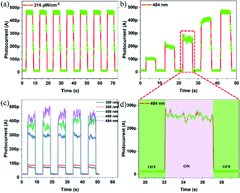 | ||
| Fig. 4 (a) Photoresponse parameters of the SPD. (b) Photoswitching photocurrent of the SPD over various power densities of illumination (increasing from 10 to 215 μW cm−2). (c) The SPD photocurrent was measured at various wavelengths with a power density of 215 μW cm−2. (d) Selected photoswitching cycle from panel (b). | ||
Fig. 5a shows the spectral response of the FSPD, with a continuously varying wavelength from 300 to 700 nm. The inset in Fig. 5a shows the optical image of the FSPD bent at about 0–90°. The obtained photoresponsivity of the flexible device at 484 nm wavelength is 22 mA W−1 with an illumination power density of 215 μW cm−2. Fig. 5b shows the I–V plots of the flexible device with light of 484 nm over various power densities of incident light illumination from 10 to 215 μW cm−2. The photocurrent reaches saturation rapidly, where a high Ps of beyond 2.2 × 10³% was achieved. Fig. 5c depicts the photoresponses of the FSPD obtained under various incident illumination power densities. Again, high photocurrent is obtained when more photogenerated carriers are excited, as a consequence of higher light intensity illumination. The τr and τf were less than 80 and 50 ms (Fig. 5d), by turning on and off the incident light illumination. The D* and NEP can be calculated for our flexible SPD to be 7.9 × 10¹⁰ Jones and 8.8 × 10⁻¹⁴ W Hz−1/2 under 484 nm illumination with a light power density of 215 μW cm−2.
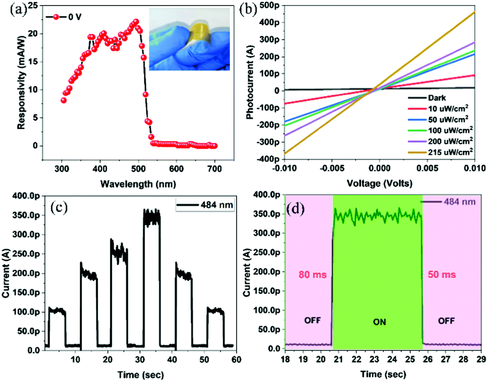 | ||
| Fig. 5 (a) Spectral response of FSPD over a wavelength of 300 to 700 nm under fixed light intensity of 215 μW cm−2. The inset is the digital image of the flexible device. (b) The I–V plots of the FSPD in the dark and over various power densities of 484 nm blue light illumination. Corresponding semi-logarithmic I–V plots are available in Fig. S2b (ESI†). (c) Photoswitching photocurrent of the flexible device with different illumination intensities. (d) Single cycle of photoswitching photocurrent from Fig. S4b (ESI†). | ||
The FSPDs were bent into various shapes and angles by altering the distance between two adjacent movable stages. After various degrees of bending, the optoelectronic stability of the FSPDs was tested. Negligible fluctuations in photocurrent of the FSPDs were found (Fig. 6a), illustrating that external bending stress has little effect on the photocurrent of the FSPD. Fig. 6b displays the I–V plots of the FSPD at various bending angles, with no significant photocurrent variation. After bending 2000 times, the photocurrent exhibits no distinct reduction, as illustrated in Fig. 6c. Moreover, before and after 2000 cycles of bending, the optoelectronic stability of 23 FSPDs was evaluated (Fig. 6d). In Fig. 6d, the abscissa and ordinate represent the device number and photocurrent ratio before and after 2000 bending cycles at zero bias, respectively. The photocurrent ratios of all the FSPDs were above 95%. So, our CdS nanobelt FSPDs constructed on PI substrates display an outstanding folding endurance, mechanical and flexural stability.
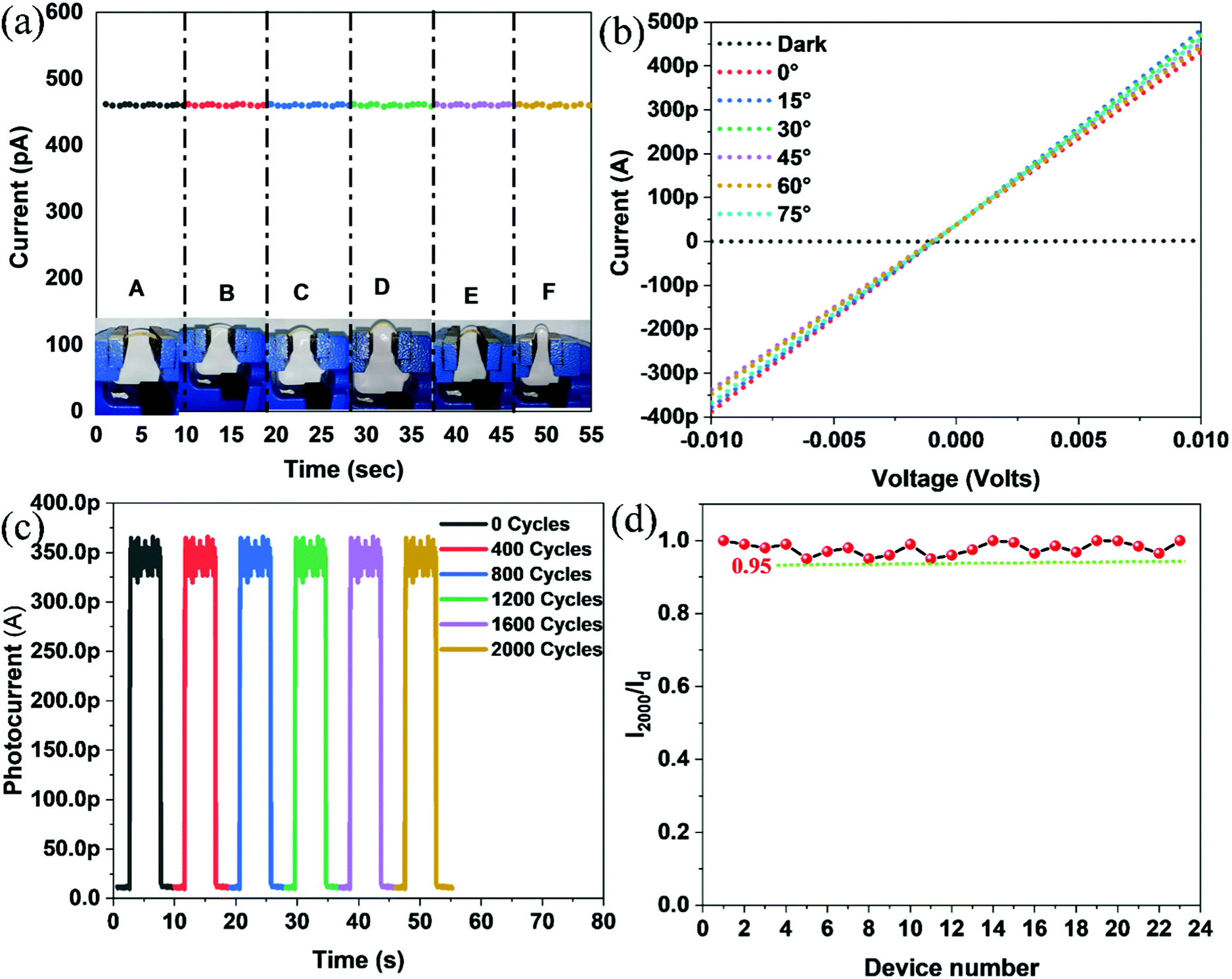 | ||
| Fig. 6 (a) The I–t plots of the flexible SPD bent at six different angles. (b) The I–V plots of the flexible SPD bent at different angles. (c) Photoswitching photocurrent of the flexible SPD obtained before and after 400, 800, 1200, 1600 and 2000 cycles of bending. (d) Stability chart of 23 FSPDs. | ||
The possible working mechanism of the present SPD was proposed on the basis of the energy band diagram (Fig. 7). To attain thermal equilibrium in the junction, electrons flow from Ag into the lower energy states in n-type CdS, which makes the surface of CdS more n-type.45 The surplus electron charge in the n-type CdS exists essentially as a surface charge density.46,47 When the SPD works under air condition, oxygen molecules adsorb on the CdS nanobelt surface and form oxygen ions by capturing free electrons from the n-type CdS [O2(g) + e− → O2−], thereby creating a depletion layer with low conductivity near the surface, which leads to the earlier depletion layer widening and the conduction and valence bands being further bent downward,48 as described in Fig. 7b. For the metal–semiconductor–metal (MSM) photodetector, the source Ag–CdS interface may provide a different interface area for the oxygen molecule adsorption from the drain Ag–CdS interface.49,50 As a result, the width of the depletion layer (W1) and barrier height (ϕ1) at the source Ag–CdS interfaces are different to those at the drain Ag–CdS interface, indicating asymmetry of the depletion layer and barrier height, as depicted in Fig. 7b. Upon illumination with photon energies above the CdS band gap, electron–hole pairs are generated. Photon-generated holes migrate to the surface and discharge the adsorbed oxygen ions [O2− + h+ → O2(g)] to photon-desorbed oxygen from the surfaces. The unpaired electrons accumulate gradually with time until desorption and readsorption of O2 reach an equilibrium state, resulting in a gradual electron and hole rise until saturation during illumination (Fig. 7c). The two-asymmetry depletion layers and barrier heights differ in ability to separate and collect the photo-generated electrons and holes, leading to the formation of net photocurrent in the external circuit without an external power supply.
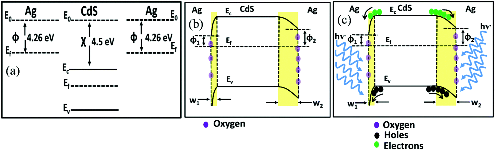 | ||
| Fig. 7 The working of present SPDs. (a) Energy band diagram, (b) in the dark and (c) under illumination. | ||
Conclusion
We report highly photosensitive and ultrafast self-powered rigid and flexible photodetectors based on 1D CdS nanobelts, obtained by a simple one-step facile vapor transport route. For the first time, asymmetric contacts are used to create extremely photosensitive and ultrafast self-powered rigid and flexible photodetectors based on 1D CdS nanobelts. The photoresponse characteristics of the constructed SPDs were outstanding, including high photosensitivity (1.54 × 10⁶%), specific detectivity (2.36 × 10¹² Jones), responsivity (36 mA W−1) and noise equivalent power (2.94 × 10⁻¹⁵ W Hz−1/2) with 215 μW cm−2 light irradiation, as well as having high reproducibility, environmental stability and speedy response of less than 30 ms. Additionally, the FSPDs showed excellent folding endurance, electrical and mechanical flexural stability. Our findings suggest that the asymmetric contact device design used in this study is appropriate for high-performance FSPDs, particularly ultrafast photodetectors.Author contributions
Muhammad Zubair Nawaz: methodology, conceptualization, writing – review, investigation, data curation, experiments, formal analysis, software, editing, and original manuscript preparation. Liu Xu: formal analysis, software, review, and editing. Xin Zhou: formal analysis, review, and editing. Khizar Hussain Shah: formal analysis and review. Jiale Wang: review and editing. Binhe Wu: review and editing. Chunrui Wang: supervision, project administration, funding acquisition, and conceptualization.Conflicts of interest
No conflicts of interest.Acknowledgements
This work was supported by the National Natural Science Foundation of China (Grant No. 61376017, 61975029 and 21703031), the NSFCNRF Scientific Cooperation Program, and the Brain Pool Program of Korea (Grant No. 171S-1-3-1829).References
- F. Withers, et al. , ACS Nano, 2013, 7(6), 5052 CrossRef CAS PubMed.
- F. H. Koppens, et al. , Nat. Nanotechnol., 2014, 9(10), 780 CrossRef CAS.
- C. M. Lieber, MRS Bull., 2003, 28(7), 486 CrossRef CAS.
- Z. Fan, et al. , Proc. Natl. Acad. Sci. U. S. A., 2008, 105(32), 11066 CrossRef CAS PubMed.
- H. Kind, et al. , Adv. Mater., 2002, 14(2), 158 CrossRef CAS.
- J. S. Jie, et al. , Nano Lett., 2006, 6(9), 1887 CrossRef CAS.
- W. Jin, et al. , J. Mater. Chem., 2012, 22(7), 2863 RSC.
- A. M. Chowdhury, et al. , ACS Appl. Mater. Interfaces, 2019, 11(10), 10418 CrossRef CAS PubMed.
- W. Tian, et al. , Small, 2017, 13(45), 1701848 CrossRef.
- W. Wu, et al. , Nano Energy, 2018, 51, 45 CrossRef CAS.
- J. Jiang, et al. , Adv. Mater. Interfaces, 2020, 7, 2000882 CrossRef CAS.
- A. Li, et al. , Adv. Mater., 2019, 31(6), e1805656 CrossRef PubMed.
- Z. Bai, et al. , J. Mater. Sci., 2017, 52(3), 1308 CrossRef CAS.
- H. Zhou, et al. , New J. Chem., 2017, 41(12), 4901 RSC.
- Y. Dai, et al. , Adv. Mater., 2018, 30(9), 1705893 CrossRef PubMed.
- R. Chai, et al. , J. Mater. Chem. C, 2019, 7(15), 4581 RSC.
- D. Wang, et al. , Semicond. Sci. Technol., 2020, 35(7), 075015 CrossRef CAS.
- X.-X. Yu, et al. , J. Mater. Chem. C, 2018, 6(3), 630 RSC.
- D. Wu, et al. , J. Mater. Chem., 2012, 22(43), 23272 RSC.
- M. Husham, et al. , Eur. Phys. J.: Appl. Phys., 2016, 74, 10101 CrossRef.
- B. Jin, et al. , Adv. Funct. Mater., 2020, 30(49), 2006166 CrossRef CAS.
- Q. Zhang, et al. , Adv. Opt. Mater., 2017, 5(5), 1600877 CrossRef.
- X. Xing, et al. , Small, 2016, 12(7), 874 CrossRef CAS PubMed.
- Y. Dai, et al. , Adv. Mater., 2018, 30(9), 1705893 CrossRef.
- C. Zhang, et al. , Nanoscale, 2014, 6(14), 8084 RSC.
- C. Wang, et al. , Mater. Res. Express, 2017, 4, 115013 CrossRef.
- T. Zhai, et al. , ACS Nano, 2009, 3(4), 949 CrossRef CAS PubMed.
- H. M. Fan, et al. , Appl. Phys. Lett., 2007, 91(17), 171911 CrossRef.
- S. Yang and J. Zhang, Appl. Phys. A: Mater. Sci. Process., 2019, 125(7), 454 CrossRef CAS.
- G. Murali, et al. , J. Alloys Compd., 2013, 581, 849 CrossRef CAS.
- G. Song, et al. , New J. Phys., 2015, 17, 063024 CrossRef.
- M. Tang, et al. , Sci. Bull., 2018, 63(17), 1118 CrossRef CAS.
- T. Gao, et al. , Appl. Phys. Lett., 2005, 86(17), 173105 CrossRef.
- S. Gupta, et al. , Nanotechnology, 2012, 23, 355702 CrossRef PubMed.
- W. Zhou, et al. , AIP Adv., 2014, 4(12), 123005 CrossRef.
- L. Li, et al. , Microelectron. Eng., 2014, 126, 27 CrossRef CAS.
- M. Husham, et al. , Superlattices Microstruct., 2014, 67, 8 CrossRef CAS.
- M. A. Mahdi, et al. , Superlattices Microstruct., 2013, 54, 137 CrossRef CAS.
- L. D. Li, et al. , ACS Appl. Mater. Interfaces, 2015, 7(42), 23507 CrossRef CAS PubMed.
- L. Sun, et al. , CrystEngComm, 2019, 21(25), 3779 RSC.
- H. Wang, et al. , Cryst. Growth Des., 2018, 18(4), 1987 CrossRef CAS.
- G. Chen, et al. , RSC Adv., 2015, 5(28), 21859 RSC.
- L. H. Zeng, et al. , ACS Appl. Mater. Interfaces, 2013, 5(19), 9362 CrossRef CAS PubMed.
- J. Shen, et al. , J. Phys. D: Appl. Phys., 2020, 53(34), 345106 CrossRef CAS.
- Y. Liu, et al. , Nature, 2018, 557(7707), 696 CrossRef CAS PubMed.
- X. Yang, et al. , J. Mater. Chem. C, 2019, 7(25), 7654 RSC.
- Q. An, et al. , Sci. Rep., 2017, 7(1), 4885 CrossRef PubMed.
- Q. An, et al. , ACS Appl. Mater. Interfaces, 2015, 7(41), 22941 CrossRef CAS PubMed.
- H.-Y. Chen, et al. , J. Mater. Chem. C, 2014, 2(45), 9689 RSC.
- D. C. Look, Mater. Sci. Eng. B, 2001, 80(1), 383 CrossRef.
Footnote |
| † Electronic supplementary information (ESI) available. See DOI: 10.1039/d1ma00580d |
| This journal is © The Royal Society of Chemistry 2021 |