
 Open Access Article
 This Open Access Article is licensed under a
 Creative Commons Attribution 3.0 Unported Licence
Recent advances in radiation detection technologies enabled by metal-halide perovskites
Tiebin
Yang
,
Feng
Li
 * and
Rongkun
Zheng
*
* and
Rongkun
Zheng
*
School of Physics, Australian Centre for Microscopy & Microanalysis, Nano Institute, the University of Sydney, NSW 2006, Australia. E-mail: feng.li2@sydney.edu.au; rongkun.zheng@sydney.edu.au
First published on 19th August 2021
Abstract
Metal halide perovskites have emerged as promising candidates for next-generation optoelectronic applications due to their high absorption coefficient, tunable bandgap, long carrier mobility, and facile solution processability. Besides these excellent physical properties, their unique features, including large bulk resistance, strong stopping power, and high mobility-lifetime product, also favour halide perovskites for radiation detection. Their excellent radiation response and radioluminescence enable them as both direct detectors and indirect scintillators with excellent figures-of-merit, even exceeding the performance of existing commercial radiation detectors. In this review, the background knowledge on ionizing radiation categorized based on the nature of the particles or electromagnetic waves and the requirements for high-performance radiation detectors are provided first. Then, the relevant fundamental characteristics and superiorities of metal halide perovskites for radiation detection are discussed in detail. Thereafter, recent achievements in detecting alpha-, beta-, gamma- and X-rays using halide perovskites are summarised. Finally, the remaining challenges and future perspectives, with particular emphasis on overcoming current obstacles, such as device stability, ion migration, and health concerns, are highlighted.
 Tiebin Yang | Tiebin Yang is currently a PhD student at the School of Physics in the University of Sydney. He received his Bachelor's degree in Physics from Nanjing University in China in 2018. His research focuses on synthesis, characterization, and applications of all-inorganic halide perovskites. |
 Feng Li | Feng Li received his PhD degree from the University of Chinese Academy of Sciences in 2014. He is currently a lecturer and a discovery early career researcher award (DECRA) fellow in the School of Physics at the University of Sydney. His main research is centered on the characterization and investigation of physical properties of functional materials, particularly hybrid perovskites and organic semiconductors, as well as diverse optoelectronic, energy and spintronic applications. |
 Rongkun Zheng | Rongkun Zheng obtained his BSc in Physics from Shandong University in China in 1999 and his PhD in Physics from the Hong Kong University of Science and Technology in 2004. He joined the University of Sydney in late 2004 and currently is a Professor in the School of Physics. His research interest spans from condensed matter and materials physics to microscopy and microanalysis, with focus on the growth-structure–property relationship in functional materials and devices. |
1. Introduction
As a type of radiation that holds enough energy to ionize atoms or molecules, ionizing radiation has been widely applied in various areas in our life.1–3 In the form of particles or electromagnetic waves, ionizing radiation can be divided into directly ionizing and indirectly ionizing, respectively. Any charged particle that has enough kinetic energy can ionize atoms through Coulomb force which induces direct ionizing. The directly ionizing radiation particles mainly include atomic nuclei, electrons, muons, charged pions, protons, and energetic charged nuclei stripped of their electrons, of which the most common types are alpha particles and beta particles that consist of helium nucleus and electrons or positrons, respectively. On the contrary, indirectly ionizing radiation is usually photon radiation or neutron radiation induced by electrically neutral particles, where the atoms will be further ionized by beta particles from the interaction of photons or neutrons with atoms. Photon radiation is typically known as high-energy electromagnetic waves, including X-rays (0.1–100 keV) and gamma-rays (0.1–100 MeV), which will cause ejection of electrons from atoms and then further ionize atoms by secondary beta particles, while neutrons often cause ionizing by interacting with protons in hydrogen via linear energy transfer. Fig. 1 clearly represents the formation of common radiation types, including particle radiation and photo radiation, and their related energies. While photo radiation can be divided into non-ionizing radiation and ionizing radiation, in our case, we mainly focus on ionizing radiation, including X-rays and gamma-rays. Thanks to their peculiarity of high penetration and ionization, radiation rays can be widely used in various fields, including nuclear physics, medical imaging, radiotherapy, food industry, security monitoring, crystallography, etc.4–8 | ||
| Fig. 1 Schematic representation of particle radiation with their formation (upper half), and the electromagnetic spectrum range from infrared to gamma-rays (lower half). | ||
In general, semiconductors with an appropriate bandgap can easily detect free charges induced by radiation under the applied voltages. Similar to the common photodetectors working in the UV–visible–infrared light ranges, semiconductor-based radiation detectors can also directly produce current signals from free-charged carriers excited by Coulomb force or through photoelectric effect. Current radiation detection devices are mainly based on silicon (Si), amorphous selenium (a-Se), germanium (Ge), cadmium zinc telluride (CZT), cadmium telluride (CdTe), and mercury iodide (HgI2).9–12 However, some prerequisites need to be fulfilled for suitable semiconductors to serve as high-performance radiation detectors. First, the semiconductors’ bandgaps are normally required to stay in the range from 1.5 eV to 2.5 eV, which can ensure a low dark current at room temperature and provide enough energy barrier for electron–hole pair production. Then, the high average atomic number Z and high mass density lead to a large stopping power for successfully detecting high-energy radiation. For instance, even though the improvements of crystal purity and doping technique have been applied for the widely-used semiconductor Si, the relatively small bandgap (1.12 eV) causes a large dark current at room temperature and the small atomic number sets a great limitation for the fabrication of high-performance Si-based radiation detectors, while the CZT materials, with a relatively large bandgap (1.57 eV) and a high atomic number of 49.3, have shown excellent performance in commercial radiation detectors, which can be operated at room temperature.13–15 Carrier mobility-lifetime product μτ is another important factor of suitable semiconductors when applied to radiation detection. A large μτ product indicates a long carrier diffusion length, by which the probability of a carrier being captured and recombined is reduced. Besides direct radiation detectors, radiation can also be detected using indirect detectors consisting of a scintillator and photodetector arrays. Scintillators can covert high-energy particles and photons into visible light via radioluminescence, which is further detected by other sensitive photodetectors such as charged-coupled devices (CCD), photodiode arrays, complementary metal-oxide semiconductors (CMOS), etc. Thus, the conversion efficiency highly determines the performance of the scintillator. To this end, high-quality scintillators should have the traits of a high light yield for generating enough detectable signals, long-term stability, and high energy resolution. Currently, the most commercially used scintillators are based on inorganic crystals, like thallium-doped sodium iodide (NaI(Tl)), thallium-doped caesium iodide (CsI(Tl)), and so on.16–18 However, these commercial semiconductors usually require complex growth methods and severe operating conditions, which create a sharp rise in the demand for new semiconducting materials with high performance, low cost and facile processing.
Over the past few years, as a family of promising photoactive materials, metal-halide perovskites with the general formula of ABX3, where the A site can be an inorganic cation like Cs+, a monovalent organic cation (typically a methylammonium (MA = CH3NH3) ion or a formamidinium (FA = CH(NH2)2) ion) or a mixture thereof, the B site is normally Pb or currently widely-researched Sn, and X is usually a halide component Cl-, Br-, I-, or a mixture thereof, have attracted much attention in the photovoltaic field,19–21 due to their excellent features, including a long carrier lifetime, large absorption coefficient, high light yield, and cost-effective growth method. Looking beyond broadly-investigated halide perovskite solar cells, the superior photophysical and electronic properties of halide perovskites also enable them as promising candidates for next-generation optoelectronic or electronic device applications, such as light-emitting diodes,22–24 lasers,25 transistors,26–29 and photodetectors.30–33
Encouragingly, metal-halide perovskites have also been demonstrated to exhibit attractive features for radiation detection applications. Since Stoumpus et al. first pointed out that metal halide perovskites have the ability to detect radiations,34 many radiation detectors based on both hybrid perovskites and inorganic perovskites have also been successfully fabricated and further improved.35–38 In this regard, the rapid research progress and great strides that have been made by metal halide perovskites in ionizing radiation detection call for a swift and consistent survey into the state of the field. Notably, recently, there have been excellent review papers spanning from lead halide perovskites to lead-free perovskite with different crystal forms which cover fundamental physical properties and the related radiation detection devices.39–41 Each of these corresponding review publications has a different line of focus, depth, and narrative. However, the reviews centered on metal halide perovskite radiation detection applications that also include the detection of the directly ionizing radiation particles are limited. Therefore, this review paper aims to comprehensively summarize the recent achievements, ongoing progress, and challenges of halide perovskites for radiation detection devices with an emphasis on fundamental detection principles of various radiation photons and charged particles as well. We begin by offering the mechanism of different types of radiation detectors. The subsequent section comprehensively presents the unique physical characteristics of metal halide perovskite materials for radiation detection. Thereafter, the recent achievements and ongoing progress on metal-halide perovskite radiation detectors in mainly detecting alpha and beta particles, as well as gamma- and X-rays are summarised and discussed in detail. At last, we conclude this research article and present a perspective for the future development of halide perovskite materials for radiation detection applications and suggest some possible strategies to improve their long-term stability and device performance.
2. Principles of radiation detectors
2.1. Direct radiation detectors
Suitable semiconductors can directly detect radiation, of which the fabricated detectors can be operated in the current or voltage modes, depending on their direct interactions of incident particles or photons with the active semiconductors.42,43Compared to alpha particles, beta particles usually hold relatively lower energy but a much higher speed, which leads to a different interaction model with atoms. Beta particles can directly interact with other electrons in atoms by inelastic scattering, which excites other electrons to high-energy level or emitting photons. However, the beta particles can also interact with the nuclei through elastic scattering due to their much lower mass during which only the trajectories of the beta particles change. Once the electron–hole pairs are generated by beta particles, they can be detected by semiconductor-based detectors in the voltage mode too.
 | (1) |
 | (2) |
2.2. Indirect radiation detection
The indirect radiation detectors are also capable of detecting high-energy particles or photons, and often consist of scintillator and photodiode arrays.47 As mentioned above, high-energy particles can ionize the active semiconducting materials by Coulomb force; while high-energy photons can interact with the materials via the photoelectrical effect, Compton scattering, and pair production. All these processes will generate many excitons in the scintillators which will be transferred to the defects states and further recombine together with UV or visible light-emitting effect. The emitted UV or visible light will be further captured by photo-sensitive photodetector arrays or cameras, and then the output is offered as a current signal or image information. The key figures of merit of scintillators are light yield (LY) and decay time. Light yield is the number of photons that can be converted by the scintillator per photon or particle energy (in unit), which can be calculated using1| LY = 106SQ/βEg | (3) |
| Quantity | Unit | Definition |
|---|---|---|
| a Parameter for direct detector. b Parameter for indirect detector. | ||
| μτ productab | cm2 V−1 | Product of carrier mobility and carrier lifetime in a radiation detector. |
| Spectral peak resolutionab | % | Defined by the ratio of full width at half maximum (FWHM) of alpha or gamma-ray peak and energy of incident ray. |
| Lowest detectable dose rateab | nGyair s−1 | The minimum detectable radiation dose rate, that is, the lowest radiation dose rate which can induce photocurrent with a signal-to-noise ratio over 3 (in X-ray detectors). |
| Spatial resolutionab | lp mm−1 | The number of line pairs that can be distinguished per millimetre. A line pair consists of a bright line and a dark line (in X-ray imaging). |
| Sensitivitya | μC Gyair−1 cm−2 | Radiation-induced charge in a detector at a specific radiation dose rate and detector volume. |
| Linear dynamic rangea | dB | The range within which the photocurrent displays a linear relationship with the incident intensity. |
| Light yieldb | ph MeV−1 | Number of photons generated by radiation with a specific energy. |
| Decay timeb | S | The time taken by the emitting light intensity excited by radiation to decay to 1/e of its initial intensity. |
3. Superb properties of halide perovskites for radiation detection
As mentioned above, the superior photophysical and electronic properties of lead halide perovskites, including long carrier lifetimes, large absorption coefficients, high light yields, and cost-effective growth methods,48–52 enable them as promising candidates for next-generation optoelectronic devices, such as light-emitting diodes,53–56 lasers,57 solar cells58–61 and photodectors.62–67 Furthermore, several prerequisites need to be fulfilled for suitable semiconductors to serve as high-performance radiation detectors. Encouragingly, lead halide perovskites have exhibited excessive properties that are actually desirable for radiation detecting devices. Currently, there is an increasing number of published reports on radiation detectors based on both hybrid halide perovskites and inorganic perovskites that have also been fabricated for detecting alpha particles, beta particles, gamma-rays, and X-rays.40,41,68 In this section, the superb features of halide perovskite materials for radiation detection applications are introduced in detail as follows:3.1. Large stopping power
Large stopping power is essential for the high-performance of radiation detectors, since more high-energy particles can be dragged down with more energy loss and thus more signal outputs. Given by the Bethe equation,69 the energy loss of charged particles passing through certain materials can be described as: | (4) |
 | ||
| Fig. 2 (a) Attenuation coefficients of CsPbI3, MAPbI3, CdTe, Se, and TlBr versus different photon energies. Reproduced with permission.39 Copyright 2019, Nature Publishing Group. (b) PL spectra of the tunable APbX3 nanocrystals. Reproduced with permission.87 Copyright 2017, AAAS. (c) Absorption coefficient and length with different photo energies of MAPbI3 crystals. Reproduced with permission.88 Copyright 2015, Nature Publishing Group. (d) Schematic of the structure of basic radiation detectors. Left: Direct detector. Right: Indirect scintillator. | ||
3.2. Suitable bandgap and large bulk resistance
As mentioned above, appropriate bandgaps for the semiconducting materials are crucial for high-performance radiation detectors, especially for room-temperature operations. Encouragingly, lead halide perovskites hold tunable bandgaps ranging from 1.3 to 3.2 eV that can be easily realized by adjusting their halide components,70–74 which make them perfectly suitable for radiation detectors (Fig. 2b and c). Meanwhile, the bulk resistances of lead halide perovskites range from 107 to 109 Ω cm, which can be further modified by tuning the halide component ratio of perovskites. The large bulk resistances ensure the low dark currents at room temperature and the low noises of the perovskite radiation detectors, especially when applied to a high voltage bias.3.3. High mobility-lifetime product
Both the intrinsic and extrinsic defects of the semiconducting materials can capture the charge carriers that are generated by radiation, thus decreasing the signal currents of the related detection devices. Large carrier-lifetime product μτ values can reduce the recombination of electron–hole pairs at the defects and traps within them, and thus more charge carriers can be collected by the electrodes which further increases the efficiency of the detector. As for the halide perovskite films, most defect centres are located at the surface or grain boundaries. To this end, several surface cleaning and passivation approaches have been applied to reduce the radiation-generated carrier recombination and thus improve the film quality.75 Among various forms of halide perovskites, grain-boundary-free single crystals usually exhibit a low trap density in the range of 107–109 cm−3 and thus offer high μτ products.76–78 For example, hybrid perovskite MAPbI3 single crystal holds a high μτ product of 10−2 cm2 V−1, with an ultralong carrier diffusion length over 175 μm under the illumination of sunlight.79 Moreover, the internal quantum efficiency of a 3 mm thick MAPbI3 single crystal can also be approaching 100% under weak light illumination, which indicates a diffusion length almost exceeding 3 mm.793.4. Facile and low-cost crystal growth method
Other advantages of halide perovskite materials and the relevant device applications include their cost-effective crystal growth and device fabrication methods. Compared to the widely-used commercial semiconductors, like Si, Ge, Se, and CZT, for which the growth processes typically require high temperature, high vacuum, or complex instruments, lead halide perovskites can usually be produced using the low-temperature (<150 °C) solution processes, such as inverse temperature crystallization (ITC),78,80 antisolvent vapor-assisted crystallization (AVC),77,81 hot inject method,48 and supersaturated recrystallization.82,83 Moreover, the total cost for the growth of halide perovskite materials is quite low as compared to that of the commonly-used semiconductor as mentioned above. For example, growing a 1 cm3 perovskite single crystal is estimated to cost around $0.3 when scaling up the production, which is 3- or 4-times lower than that for CZT crystals.39 Besides, the related detection devices can be easily fabricated via a one-step spin-coating or spray method and directly using the freshly-grown perovskite crystals, which offers a large operation room for further integration.3.5. High light yield
The fascinating properties of lead halide perovskites can also enable them as both direct photoconductors and indirect scintillators for radiation detection. When transforming into different crystal forms, like nanocrystals and quantum dots, lead halide perovskites exhibit strong radioluminescence under the excitation of high-energy radiations. For instance, as compared to LaBr3–Ce, which exhibited optimal device performance with a light yield (LY) of 70![[thin space (1/6-em)]](https://www.rsc.org/images/entities/char_2009.gif) 000 ph MeV−1 and a decay time of 16 ns, lead halide perovskites hold a much higher light yield (LY) over 106 ph MeV−1 and a fast decay time less than 1 ns.84 Such high light yield (LY) and fast decay time ideally meet the requirement for first-class scintillators, which enable them to measure the time of initial particle or radiation with high precision and timing resolution. Besides, halide perovskite nanocrystals also permit easy halide ion exchanges, from which a tunable luminescence spectrum across almost the whole visible region can be obtained.85,86
000 ph MeV−1 and a decay time of 16 ns, lead halide perovskites hold a much higher light yield (LY) over 106 ph MeV−1 and a fast decay time less than 1 ns.84 Such high light yield (LY) and fast decay time ideally meet the requirement for first-class scintillators, which enable them to measure the time of initial particle or radiation with high precision and timing resolution. Besides, halide perovskite nanocrystals also permit easy halide ion exchanges, from which a tunable luminescence spectrum across almost the whole visible region can be obtained.85,86
Armed with these unique advantages, direct radiation detectors based on halide perovskite single crystals and polycrystalline films have exhibited excellent device performance in a photoconductor mode.35,88–93Fig. 2d shows the common device structure of the halide perovskite direct radiation detector, which is composed of a perovskite layer and two electrodes in the left part. The right side in Fig. 2d displays the schematic diagram of the perovskite-based indirect detector which normally consists of a perovskite scintillator and another photodetector array. Excellent compatibility and easy fabrication methods also enlarge the room for further improving the device performance. Besides, due to their high light yield under radiation, lead halide perovskites can serve as scintillators integrated with other semiconductor-based photodiodes, by which high-performance radiation detectors can be achieved with multiple detection abilities.94–96
4. Charged particle detection by lead halide perovskites
4.1. Alpha-particle detectors
In 1899, the alpha particles were named by Rutherford as they have the lowest penetration of ordinary objects; and in 1907, these particles were then confirmed as helium nuclei.97 Emitted from the alpha decay of heavy atoms, alpha particle energy varies with the half-life of the emission process, where the higher energy is caused by the larger nucleus. Most alpha particles can hold energy ranging from 3 to 7 MeV, with a speed of 15000 km s−1 due to their higher particle mass as compared to other radiation rays. Thus, the penetration of the alpha particles is typically lower than that of beta particles or gamma rays, and can be blocked by a piece of paper or human skin. However, it is still the most destructive ionizing radiation; if alpha-emitting atoms are inhaled, ingested, or injected into our body, they will cause serious chromosomal damage to DNA which is 20 times greater than that caused by the same dose of gamma-rays or beta particles.98 In this regard, developing high-quality detectors for alpha particle radiation would be of significance, as they will be of use not only for environmental safety concerns but also for the nuclei information carried out by alpha particles. An alpha spectrum is commonly used to characterize alpha particles that are emitted from the nuclei. Thus peak resolution is an important parameter for alpha radiation detectors, which helps distinguish the alpha radiation peak in the alpha spectrum. As mentioned in the above section, another key parameter of alpha particle detectors is the μτ product, which is directly related to the charge collection efficiency (CCE) and can be derived from the Hecht equation for single carrier:99,100 | (5) |
Recently, Xu et al. fabricated alpha particle detectors based on hybrid perovskite MAPbBr3 single crystals (5 mm × 5 mm × 2 mm) with a metal–semiconductor–metal structure.101 As shown in Fig. 3a, the organic BCP and C60 layers were coated for the functions of both passivation and electron extraction, and a preamplifier and a digitizer were used for alpha spectrum measurements. A series of alpha energy spectrums were obtained under the exposure of a 0.8 μCi 241Am source for 900 s at different biases. A voltage-dependent alpha spectral peak with a voltage bias changing from 180 V to 550 V can be clearly observed, as shown in Fig. 3b. From the Hecht equation of single-polarity charge transport, the calculated hole mobility-lifetime μτ product could be (0.4–1.6) × 10−3 cm2 V−1 (as shown in Fig. 3c). However, the relatively high device dark current (200 nA) apparently limits the device performance. To this end, He et al. firstly reported the alpha particle detector based on an all-inorganic perovskite CsPbBr3 with an asymmetric In/CsPbBr3/Au structure.91 The crystal was grown by the Bridgman method and cut into 3 mm × 3 mm × 1 mm for device fabrication. Due to the large difference in work functions between the In (ϕIn = 4.1 eV) and Au (ϕAu = 5.1 eV) electrodes, the large potential barriers for both hole and electron can be formed on the In and Au sides, respectively, which further suppressed the dark current of the device under reverse bias. As shown in Fig. 3d and e, a low dark current of 2 nA cm−2 was obtained at −1 V, and it could be increased to 100 nA cm−2 at a bias of −100 V; while a large dark current of 300 nA cm−2 at a 100 V forward bias was obtained. A voltage-dependent alpha spectral peak was also shown in all-inorganic perovskite alpha radiation detector (as shown in Fig. 3f), with a peak resolution of 15%. Notably, this alpha particle detector can be operated at a low bias of −6 V compared to other perovskite-based alpha particle detectors which usually require large operation voltages. The hole mobility-lifetime product of 9.4 × 10⁻⁴ cm2 V−1 was obtained from fitting the Hecht equation (Fig. 3g), which exhibits the competitive device performance of all-inorganic perovskites working for alpha particle detectors.
 | ||
| Fig. 3 (a) Schematic illustration of the alpha particle detector based on MAPbBr3 single crystal with the size of 5 × 5 × 2 mm3. (b) Voltage-dependent alpha spectra obtained from MAPbBr3 single crystal detector. (c) Spectral peak centroids at different voltage biases. Black points represent experimental data, with a red line fitted from the Hecht equation. Reproduced with permission.101 Copyright 2017, Elsevier. (d) I–V curve characterization of In/CsPbBr3/Au alpha particle detector with the structure of In/CsPbBr3 (3 × 3 × 1 mm3)/Au under the dark condition at bias from −1 V to 1 V. (e) Temporal I–V characterization of the In/CsPbBr3/Au detector under forward and reverse applied bias conditions. (f) Voltage-dependent alpha spectra were obtained under different reverse biases. (g) Mobility-lifetime product calculation for hole obtained by fitting the Hecht equation. Reproduced with permission.91 Copyright 2019, Elsevier. | ||
Besides direct alpha particle detectors, lead-based halide perovskites can also be suitable for fabricating indirect scintillators for detecting alpha particles. The most outstanding merit of halide perovskite-based scintillators is their fast response speed, which usually lies in the magnitude of nanosecond. Mykhaylyk et al. reported high light-yield (LY) alpha particle scintillators based on hybrid perovskite MAPbBr3 nanocrystals with an ultrafast response time at low temperature.84 As depicted in Fig. 4a, hybrid perovskite MAPbBr3 shows an increasing light output yield with decreasing temperature, which is much higher than those of the commercial LYSO-Ce-based scintillators at around 150 K and CsI-based scintillators at around 50 K. Moreover, hybrid perovskite MAPbBr3 also exhibited a rapid and intense alpha response with fast and slow decay times of 0.1 ns and 1 ns, respectively, at 77 K compared to the relatively longer decay of 1 μs for LYSO-Ce (Fig. 4b). Fig. 4c shows the pulse height spectra of the scintillators based on MAPbBr3 and CsI with a distinct Gaussian shape peak of 5.5 MeV alpha particle from 241Am source, which exhibited the comparable alpha detecting ability of MAPbBr3 with that of the commercial scintillators.
 | ||
| Fig. 4 (a) Scintillator light output measurement as a function of temperature for MAPbBr3 (black), LYSO-Ce (red), and CsI (green) under 241Am source. (b) Normalised scintillator decay of MAPbBr3 crystal (red) and LYSO-Ce (black). (c) Alpha pulse height spectra of MAPbBr3 and CSI scintillator at 50 K. The pulse height distributions that signify the scintillation response are fitted by Gaussian fitting (red lines). Reproduced with permission.84 Copyright 2019, RSC. (d) Pulse height spectra of Li-doped (PEA)2PbBr4 with Gaussian fitting to extract light yield. (e) Alpha pulse height spectra of (PEA)2PbBr4 scintillator. Reproduced with permission.102 Copyright 2020, Nature publishing group. | ||
Currently, lithium-doped 2D lead halide perovskite (PEA)2PbBr4 is also being used for multiple radiation detectors and scintillators, which was reported by Xie et al. for the first time.102 With a lithium dopant, light yield of (PEA)2PbBr4-based devices could be increased up to 11000 ph MeV−1, and a fast decay time of 11 ns was also obtained (in Fig. 4d). Fig. 4e displays the pulse height spectra results of the (PEA)2PbBr4 scintillator under radiation from 241Am and 224Cm sources. Table 2 summarizes the figures of merit of halide perovskite-based alpha detectors. Compared to the commercial alpha particle detectors and scintillators which require high-cost production lines, lead-based halide perovskites, taking the obvious advantages of low cost and multiply functional detectability, have already shown impressive potential for next-generation alpha particle detection applications.
4.2. Beta particle detectors
Holding a moderate penetration ability, beta-rays, usually consisting of electrons or positrons, play an important role in surface radiative contamination surveillance103 and cancer cell treatment.104 Beta particles can interact with atoms by elastic scattering and inelastic scattering. As mentioned above, elastic scattering happens when beta particles are scattered with nuclei which only changes the trajectory and inelastic scattering happens between beta particles and electrons in atoms which produces other electrons or photon signals. The ratio between elastic scatter and inelastic scatter η is higher for the element with a larger Z, which means that more inelastic scatterings happen in the low-Z elements and thus more photons are emitted and high scintillator performance can be obtained. Recently, beta-ray scintillators were mainly fabricated using organic single crystals, liquids, or plastics, which usually suffer from high production cost, carcinogenicity, complex fabrication, and poor thermal stability.105,106 Currently, Yu et al. reported a new type of beta-ray scintillator based on 2D lead halide perovskite (A)2PbBr4,37 in which the organic cations can be butylamine (BA), octylamine (OA), stearamine (STA), or dodecylamine (DA). A series of 2D lead halide perovskites were synthesized through a facile solution process, as shown in Fig. 5a–d. After adding Mn2+ as the emission centre, 2D lead halide perovskites show a significant increase in PL-QY values, as shown in Fig. 5e–h. Fig. 5i displays the working set-up of a beta-ray scintillator based on 2D lead halide perovskite with scintillation signal captured using a CCD camera. Moreover, the resultant beta particle scintillator exhibited a low detection limit of 0.1 mCi (Fig. 5j and k) and a high decomposition temperature of 300 °C compared to that in the range of 70–105 °C for the commercial plastic beta-ray scintillators. Taking the combined advantages of the organic cations for beta-particle detection and the perovskite structure for high PL-QY values, hybrid 2D lead halide perovskites shed light on high-performance beta-ray detectors. | ||
| Fig. 5 (a)–(d) SEM images of 2D lead halide perovskites BA2PbBr4, OA2PbBr4, DA2PbBr4, and STA2PbBr4. (e)–(h) PL QY measurement before and after Mn2+ addition, with an obvious increase. (i) Set-up for 2D perovskite-based beta-ray scintillator. (j) Scintillation spectra of 2D perovskites under different beta-ray radiation intensities. (k) Scintillation spectra at a beta-ray radiation intensity of 0.1 mCi. Reproduced with permission.37 Copyright 2019, Nature Publishing Group. | ||
5. Photon-radiation detection by lead halide perovskites
5.1. Gamma-ray detectors
Gamma-rays, as a form of electromagnetic waves, have the shortest wavelength and the highest energy, and are usually emitted from atomic nuclei. Gamma-rays can also be detected using an indirect scintillator or direct photodetector that records a gamma-ray spectrum through the voltage mode. So, the most important figure of merit of a gamma-ray detector is gamma energy resolution, which can be defined as the ratio between the FWHM of the gamma-ray peak and the gamma-ray's energy. Similar to the other photons, gamma-rays show an exponential decay in their intensity when they pass through objects. The gamma-ray intensity can be given by| I = I0e−μx | (6) |
Compared with the halide perovskite polycrystalline films which suffer from high trap density and defects induced from grain boundaries, halide perovskite single crystals with appropriate thickness and low trap density have gained favors for gamma-ray detectors. Yakunin et al. reported the fabrication of the gamma-ray detectors based on FAPbI3 single crystals at room temperature for the first time.109 In this work, two large-sized (3–12 mm) hybrid perovskite MAPbI3 and FAPbI3 single crystals were grown through a facile solution-processed method. Fig. 6a shows the photocurrent measured as a function of voltage bias under the radiation of Cu Kα X-ray. By fitting the data using the Hecht equation, perovskite MAPbI3 exhibited a high μτ product of around 10−2 cm2 V−1. The fabricated gamma-ray detector based on FAPbI3 also showed a good response under radiation from 241Am, as shown in Fig. 6b. However, the FWHM of the gamma-ray detectors was only 35%, which was limited by the large dark current and poor phase stability of the FAPbI3 single crystals at room temperature. Then, He et al. also demonstrated a well-resolved gamma-ray spectrum via using the MAPbI3 single crystals.110 Constructed by an asymmetric Ga/MAPbI3/Au structure, the dark current was successfully suppressed to less than 100 nA at a 100 V reverse bias (Fig. 6c). Fig. 6d depicts the gamma-ray spectrum measured using a Ga/MAPbI3/Au photodetector, where a superb peak resolution of 6.8% was achieved under the radiation of 122 keV of 57Co source. However, the relatively low bandgap and bad thermal stability of MAPbI3 single crystals set a huge limit for their usage in high-energy gamma-ray detection applications. Compared to MAPbI3, both MAPbCl3 and MAPbBr3 are more thermally stable under radiation conditions and can also be synthesized via a solution process. Wei et al. reported a high-performance gamma-ray detector by further modifying the halide component ratio in MAPbBrxCl3−x single crystals.89 As the halide component varied from totally Br to Cl, hybrid perovskite single crystals showed a clear transition from the p-type transport to the n-type behaviour. Particularly, it is found that the mixed hybrid perovskite MAPbBr2.94Cl0.06 single crystal was almost intrinsic, thus leading to a ten-fold improved bulk resistivity of 3.6 × 10⁹ Ω cm. The dopant technique also offered an increased μτ product of 1.8 × 10⁻² cm2 V−1. Besides crystal quality improvement via the dopant strategy, efficient device designs also made a great contribution to the radiation detecting performance. As shown in Fig. 6e, the surface/edge leakage current was mitigated by a guard ring electrode. Being capable of detecting higher-energy gamma-rays, the MAPbBr2.94Cl0.06 photodetector exhibited a resolution of 6.5% under 665 keV gamma-ray radiation from a 137Cs source (Fig. 6f).
 | ||
| Fig. 6 (a) Bias dependency of photocurrent in MAPbI3 single crystals generated by Cu Kα X-rays at 8 KeV. The red line indicates a fitting from the Hecht equation with μτ of 10−2 cm2 V−1. (b) Energy resolved spectrum of 241Am by FAPbI3 single crystal. Reproduced with permission.109 Copyright 2016, Nature Publishing Group. (c) I–V curve of Ga/MAPbI3/Au photodetector under dark conditions. (d) Energy resolved spectrum of 57Co by MAPbI3 single crystals. Reproduced with permission.110 Copyright 2017, ACS. (e) Left: Top view of the guard ring electrode side of MAPbBr2.94Cl0.06 photodetector. Right: Top view of the anode electrode side. (f) Enlarged image of the photopeak region from 137Cs spectrum obtained using MAPbBr2.94Cl0.06 photodetector (red) and MAPbBr3 photodetector. Reproduced with permission.89 Copyright 2017, Nature Publishing Group. | ||
Besides hybrid lead halide perovskites, all-inorganic lead halide perovskites, in which organic cations are usually replaced by inorganic cation Cs+, also hold huge potential for gamma-ray detection. All-inorganic perovskite CsPbBr3 has a high average atomic number of 65.9 which is much higher than that of CZT (50.2), thus leading to a larger attenuation coefficient and a higher stopping power. He et al. have successfully obtained a high-resolution gamma-ray spectrum by using CsPbBr3 crystals.35 Grown using the Bridgman technique, perovskite CsPbBr3 single crystal can be easily diced into different shapes (Fig. 7a). Asymmetric device structure with CsPbBr3 single crystal working as the active layer was also applied in this work with Ga and Au used as electrodes. As mentioned above, because of the different Work Functions between the Ga and Au electrodes, the dark current was highly suppressed even under high reverse bias. Fig. 7b and c show the dark current characterization of the asymmetrically-structured Ga/CsPbBr3/Au and the symmetrically-structured Au/CsPbBr3/Au devices, respectively, where the asymmetric devices displayed a 104-times lower dark current at −200 V bias. Noticeably, CsPbBr3 also maintained a good μτ product of 1.34 × 10⁻³ cm2 V−1. Furthermore, when exposed to a 5 μCi 137Cs source, the asymmetric photodetector achieved a peak resolution of 3.8% at 662 keV (Fig. 7d). Recently, He et al. also reported a gamma-ray photodetector with an asymmetric In/CsPbBr3/Au structure,91 which was capable of detecting both alpha-particles and gamma-rays. Sharing a similar principle, a 4.8% photopeak resolution under the radiation of 57Co source at 122 keV was achieved. Lately, He et al. further improved the device structure via using a low work-function metal in the eutectic Ga–In alloy (EGaIn),111 which enabled a record-high gamma-ray peak resolution of 1.4% by the EGaIn/CsPbBr3/Au gamma-ray detector with a planar structure (Fig. 7e). However, the planar-structured radiation detector suffers from a decrease in peak resolution when enlarging the crystal size. With a hemispherical device structure as shown in Fig. 7f, a unipolar radiation device with electrons being screened was obtained, and a larger-sized CsPbBr3 crystal can be applied into this gamma-ray detector with a high peak-resolution of 1.8%.
 | ||
| Fig. 7 (a) CsPbBr3 single crystal grown using the Bridgman technique. (b) I–V curve of the Ga/CsPbBr3/Au asymmetric device. (c) I–V curve of the Au/CsPbBr3/Au device, with a large dark current at −200 V. (d) Gamma spectrum obtained by CsPbBr3 single crystal under radiation from 137Cs source. Reproduced with permission.35 Copyright 2018, Nature Publishing Group. (e) Gamma spectrum obtained by CsPbBr3 single crystals with different device structures under radiation from a 137Cs source. (f) Schematic illustration of the device operation principle of planar and hemispherical gamma-ray detectors and the corresponding device pictures. Reproduced with permission.111 Copyright 2020, Nature Publishing Group. | ||
Lead-based halide perovskites have also been used in indirect gamma-ray scintillators, owing to their high photoluminescence (PL) and light-emitting properties. Recently, Xu et al. reported a gamma-ray scintillator based on hybrid perovskite MAPbBr0.05Cl2.95 single crystal.112 In this work, a series of MAPbBrxCl3−x single crystals were grown via a solution-processed method, and then the obtained single crystals were further integrated onto the silicon photomultiplier (SiPM) window as the scintillators. Fig. 8a and c show the PL spectrum of MAPbBrxCl3−x single crystals by tuning the ratio of Br and Cl components. A near-band-edge emission was obtained for MAPbBr0.05Cl2.95 single crystal. The pulse height spectra of 1.7 μCi 137Cs source were successfully acquired at room temperature (as shown in Fig. 8b). Furthermore, 0D all-inorganic halide perovskite-based gamma-ray scintillators were also fabricated by Xu and his colleagues.90 0D Cs4PbBr6 embedded with CsPbBr3 nanocrystals was synthesized by a facile solution method. The obtained 0D Cs4PbBr6/CsPbBr3 nanocrystal composites were further coated onto a photomultiplier tube (PMT) for fabricating gamma-ray scintillators, as shown in Fig. 8d. Fig. 8e exhibits the obtained pulse height spectra under the radiation from 241Am, where a high resolution of 3.0% was achieved by the 0D Cs4PbBr6/CsPbBr3-based scintillator compared with that of the commercial NaI(Tl) (resolution of 17.8%). Moreover, a fast decay time of 10 ns and a high light yield of 64000 ph MeV−1 were obtained as well. Besides the 3D- and 0D-formed halide perovskites (like CsPbBr3 crystals and 0D Cs4PbBr6 materials embedded with CsPbBr3 nanocrystals), layered halide perovskite (C6H5C2H4NH3)2PbBr4 has also shown good scintillation when excited by gamma-rays.113 In the work, the large-sized (27 × 13 × 4 mm) layered perovskite crystals were synthesized by a solution-processed method. The bulk crystal sample showed a high light yield of 14000 ph MeV−1 and a fast decay time of 11 ns. Table 3 summarizes the figures of merit of the lead halide perovskite-based gamma-ray detectors and other commercial gamma-ray detectors based on other materials. Even though halide perovskite-based gamma-ray detectors have a relatively lower resolution (about 1%) as compared with the state-of-the-art CZT gamma-ray detector, its low-temperature growth method and reasonable production cost indisputably blaze a new way for new generation gamma-ray detectors which are capable of both direct and indirect detection applications.
 | ||
| Fig. 8 (a) X-Ray induced photoluminescence of MAPbBrxCl3−x single crystals. (b) Pulse height spectra acquired by MAPbCl3 and MAPbBr0.05Cl2.95 under the radiation of a 1.4 μCi 137Cs source. Reproduced with permission.112 Copyright 2019, ACS. (c) Optical images of MAPbBrxCl3−x single crystals excited by a 365 nm laser. (d) Schematic of gamma-ray scintillator set up. (e) Pulse height spectra acquired by the commercial NaT(Tl) and CsPbBr3/Cs4PbBr6 scintillator under the radiation of 241Am source. Reproduced with permission.90 Copyright 2020, RSC. | ||
| Material | Bandgap (eV) | μτ product (cm2 V−1) | Source | Energy resolution (%) | Ref. |
|---|---|---|---|---|---|
| HPGe | 0.66 | >1 | 137Cs | 0.2 | 39 |
| CZT | 1.5–1.6 | >10−2 | 137Cs | 0.5 | 107 |
| MAPbI3 | 1.5 | 0.8 × 10⁻³ | 57Co | 6.8 | 110 |
| MAPbBr2.94Cl0.06 | 2.2 | 1.8 × 10⁻² | 137Cs | 6.5 | 89 |
| CsPbBr3 | 2.3 | 1.3 × 10⁻³ | 137Cs | 3.8 | 35 |
| CsPbBr3 | 2.3 | 8 × 10⁻³ | 137Cs | 1.4 | 111 |
| MAPbBr0.05Cl2.95 | 3.0 | — | 137Cs | 10.5 | 112 |
| Cs4PbBr6/CsPbBr3 | — | — | 241Am | 3.0 | 90 |
| NaI(Tl) | 3.0 | — | 137Cs | 5.6 | 114 |
5.2. X-Ray detectors
X-Rays, as a kind of electromagnetic wave with high penetration, is one of the most widely-used forms of radiation in modern society. Since their discovery by Rontgen in 1895, X-rays were immediately applied into the field of medical applications due to their high sensitivity to different materials and thus enabled high-resolution imaging applications.115 In the 20th century, X-rays have shown their ability in the areas of crystallography, imaging, microscopy, and even been used in World War I. Nowadays, the application of X-rays covers more broad fields, including medicine, food safety, environmental surveillance, industry, science research studies, etc.2,6,116 Similar to gamma-rays, X-rays can be detected using either direct photodetectors coupled with semiconductor photodiodes or indirect scintillators. While aiming to get high imaging performance, extra consideration of sensitivity, spatial resolution, and lowest detectable dose rate need to be taken for X-ray detectors.684 μC Gyair−1 cm−2 under a 5.0 V mm−1 electric field (Fig. 9d). The all-inorganic components enabled excellent film stability with only a slight reduction in sensitivity after exposure to air for 9 months. Gou et al. have also successfully grown high-thickness CsPbBr3 polycrystalline films for X-ray detection applications.118 A dissolve-recrystallization method was used to improve the film quality, which further enhanced the device performance with a high sensitivity of 470 μC Gyair−1 cm−2 at zero bias under a low X-ray dose radiation of 0.05 μGyair s−1. Synthesized by a facile hot-injection solution process, CsPbBr3 quantum dots (QDs) can also be used in the devices that can exhibit promising X-ray response performance.119 Moreover, flexible X-ray detectors based on CsPbBr3 QD arrays were also fabricated on a PET substrate using the inkjet printing method (Fig. 9e). This easily printable X-ray detector can detect a low dose of 17.2 μGyair s−1 with a sensitivity of 1450 μC Gyair−1 cm−2, as shown in Fig. 9f.
 | ||
| Fig. 9 (a) MAPbBr3 single crystals grown at different MABr/PbBr2 ratios. (b) X-Ray induced photocurrent at different dose rates. Reproduced with permission.38 Copyright 2016, Nature Publishing Group. (c) SEM image of CsPbBr3 thick films grown via the hot press method. (d) Sensitivity and gain factor of X-ray detector at the various electric fields. Reproduced with permission.92 Copyright 2019, Wiley-VCH. (e) CsPbBr3 QD array on a flexible PET substrate. (f) X-Ray excited photocurrent and sensitivity at different dose rates. Reproduced with permission.119 Copyright 2019, Wiley-VCH. | ||
 | ||
| Fig. 10 (a) Photograph (left) and the corresponding X-ray image (right) obtained using a MAPbI3 photodetector. Reproduced with permission.88 Copyright 2016, Nature Publishing Group. (b) Solid connection between MAPbBr3 single crystal and Si wafter integrated by a small molecule. (c) Optical and X-ray images of a capsule with a steel spring and a fish fin. Reproduced with permission.120 Copyright 2017, Nature Publishing Group. (d) Optical image of MAPbI3 on TFT backplane. Inset shows a pixel structure of TFT. (e) A hand phantom X-ray image was obtained using a MAPbI3 photodetector. Reproduced with permission.36 Copyright 2017, Nature Publishing Group. | ||
Compared to the direct X-ray detector, halide perovskite X-ray scintillators are more suitable for real-time X-ray imaging applications due to their superb light yield and ultrafast photoresponse. As mentioned above, halide perovskite QDs and nanocrystals exhibited tunable radioluminescence properties with high light yield under excitation from X-rays or gamma-rays,121,122 which enable them as high-performance X-ray scintillators. Heo et al. fabricated X-ray scintillators based on all-inorganic perovskite CsPbBr3 nanoparticles,123 which comprised a carbon fiber reinforced polymer (CFRP), CsPbBr3 nanoparticles, and Si-PD arrays (as shown in Fig. 11a and b). The spatial resolution of the X-ray detector is 9.8 lp mm−1, which is almost the same as that of the commercial CsI(Tl) scintillator (10 lp mm−1) and is much higher than that of gadolinium oxysulfide (GOS) scintillator (6.2 lp mm−1). Fig. 11c shows the X-ray detection images obtained from both the CsPbBr3-based scintillator and the GOS-based scintillator. Even with decreasing X-ray dose, the CsPbBr3-based scintillators can still hold the good image contrast as compared to the GOS-based scintillators. Recently, flexible X-ray detectors based on CsPbBr3 QDs were also fabricated on photomultiplier tube (PMT) substrates via a facile spin-coating method.124 As shown in Fig. 11d, the X-ray detectors exhibited a clear linear radioluminescence in relation with different X-ray dose rates. Moreover, a lowest detectable dose rate of 13 nGyair s−1 from these detection devices was achieved, which is over 400-times lower than the medical diagnostic baseline. Fig. 11e exhibits the real-time X-ray imaging setup of a flexible detector for a biological sample, where steel can be clearly found inside the insect body (as shown in Fig. 11f). Except for the all-inorganic perovskite QDs, CsPbBr3 nanosheets with a high X-ray excited light-yield could also be fabricated into X-ray scintillators. Zhang et al. reported a large-scale (72 cm2) X-ray scintillator based on CsPbBr3 nanosheets,125 which showed a good image resolution of 0.21 mm. Lead-based halide perovskites have already exhibited their outstanding capacity for both X-ray detection and imaging in the past few years, keeping the gap between them and the commercial detectors more and more narrowing. Table 4 shows the key parameter comparison of currently reported halide perovskite-based X-ray detectors.
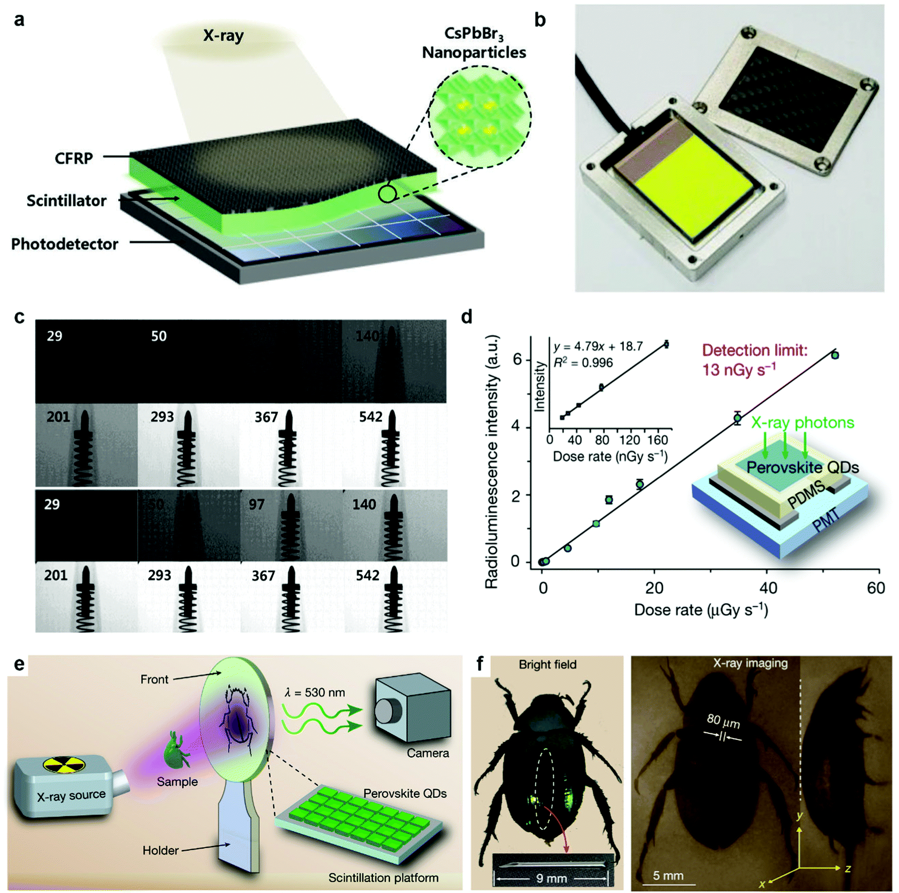 | ||
| Fig. 11 (a) Schematic illustration of the CFRP/CsPbBr3/SiPD X-ray detector. (b) Photograph of the CsPbBr3 based X-ray detector. (c) X-Ray images obtained using the GOS scintillator (top) and CsPbBr3 detector (bottom) under different X-ray dose rates. Reproduced with permission.123 Copyright 2018, Wiley-VCH. (d) Radioluminescence intensity of a flexible X-ray scintillator at different dose rates. (e) Set up for real-time X-ray diagnosis of biological samples. (f) Bright-field image (left) and the corresponding X-ray image (right) of the biosample. Reproduced with permission.124 Copyright 2018, Nature Publishing Group. | ||
| Material | μτ product (cm2 V−1) | Sensitivity (μC Gyair−1 cm−2) | Lowest detectable limit (Gyair s−1) | Spatial resolution (lp mm−1) | Ref. |
|---|---|---|---|---|---|
| MAPbBr3 single crystal | 1.2 × 10⁻² | 80 | 0.5 μ | — | 38 |
| MAPbI3 polycrystal film | 2 × 10⁻⁴ | 2527 | — | 117 | |
| CsPbBr3 quasi single crystal | 1.3 × 10⁻² | 55684 |
215 n | — | 92 |
| CsPbBr3 polycrystal film | — | 470 | 0.05 μ | — | 118 |
| CsPbBr3 QD arrays | — | 1450 | 17.2 μ | — | 119 |
| MAPbBr3 single crystal | 4 × 10⁻³ | 21000 |
36 n | 10 | 120 |
| MAPbI3 films | 1.0 × 10⁻⁴ | 11000 |
10 μ | 3.1 | 36 |
| CsPbBr3 nanoparticles | — | — | 30 | 9.8 | 123 |
6. Non-lead halide perovskites for radiation detection
Except for the lead halide perovskite-based radiation detectors, non-lead halide perovskites have also attracted enormous research interests due to their environmentally safe nature. For example, the double perovskites (A2BB′X6) and the defect perovskites (A3M2X9) have also shown a huge potential for radiation detection applications, in which the common Pb component is usually replaced by other heavy elements, such as Bi, Sb, and Ag.126–129 McCall et al. synthesized A3M2I9 (A = Cs, Rb; B = Bi, Sb) defect perovskites for alpha-particle detection.130 These perovskites all have high average atomic numbers from 49 to 58, which offer them enough attenuation coefficients and high stopping powers for radiation detection. However, it should be noted that these perovskite materials also have their own disadvantages, that is, the μτ products of these perovskites are only around 10−5 cm2 V−1. In this regard, replacing the inorganic elements Cs and Rb with NH4 group would be an effective approach. Zhuang et al. fabricated highly sensitive X-ray detectors based on (NH4)3Bi2I9 single crystals.131 Encouragingly, the (NH4)3Bi2I9 single crystals held a high μτ product of 10−2 cm2 V−1, which is comparable to those of MAPbBr3 and CZT single crystals. The relevant X-ray photodetector showed a lowest detectable dose rate of 55 nGyair s−1. Zheng et al. have reported an X-ray detector based on MA3Bi2I9 single crystal with a much lower detectable limit of 0.62 nGyair s−1.132 (Fig. 12a and b). The anisotropic properties of MA3Bi2I9 single crystals led to a large resistance in the out-of-plane direction, by which a high sensitivity of 10620 μC Gyair−1 cm−2 was achieved. Double perovskite Cs2AgBiBr6 has also attracted huge research attention for X-ray detection, due to its high average atomic number of 53.1. Pan et al. reported Cs2AgBiBr6 single crystals with the large bulk resistances in the range of 109–1010 Ω cm,133 which further suppressed the dark current when applied in X-ray detectors. The all-inorganic components also enhanced thermostability, by which the single crystals can endure thermal stress up to 430 °C (in Fig. 12c). As shown in Fig. 12d, the lowest detectable limit of the related X-ray detectors is 59.7 nGyair s−1 with a μτ product of 10−3 cm2 V−1. But, it should be pointed out that the sensitivity of Cs2AgBiBr6-based X-ray detector is relatively low (105 μC Gyair−1 cm−2). More recently, the photophysical behavior of the Cs2AgBiBr6 X-ray detector has been studied by Steele et al.,134 where they found that the radiation-induced charge carriers were less susceptible to scattering at lower temperatures and the resistance of Cs2AgBiBr6 was significantly increased as well, thus an improved device sensitivity of 2100 μC Gyair−1 cm−2 was obtained. These non-lead perovskite-based radiation detectors have shown their promising potential for radiation detection application, which may further make the environmentally-safe halide perovskite detectors highly possible.
 | ||
| Fig. 12 (a) Photograph of MA3Bi2I9 single crystals. (b) X-Ray dose-dependent signal-to-noise ratio of the out-of-plane device with the lowest detectable dose of 0.62 nGyair s−1. Reproduced with permission.132 Copyright 2020, Elsevier. (c) Thermogravimetric analysis of Cs2AgBiBr6. Included is a photograph of the Cs2AgBiBr6 single crystal. (d) The signal-to-noise ratio of the device under different voltages and X-ray doses. Reproduced with permission.133 Copyright 2017, Nature Publishing Group. | ||
7. Challenges and outlook
Metal-halide perovskites have attracted tremendous research attention for various energy-related and optoelectronic applications in the past decade, due to their high absorption coefficients, long diffusion lengths, superb light yields, and high carrier mobilities. So far, many halide perovskite-based radiation detectors have also been reported, because of their fast and excellent response to the charged particles and photon radiation. These outstanding photophysical and transport properties of metal halide perovskites enable them as direct radiation detectors with high sensitivity and spectral resolution. Besides, metal halide perovskites can also be fabricated into scintillators working in the indirect mode due to their efficient light-emitting features under all types of radiation. Notably, metal halide perovskites can be easily integrated with other semiconductors for radiation detectors, which even hold superior device performance when appropriate device design is applied. Moreover, compared with today's commercial radiation detectors, like X-ray imagers, the detectors based on halide perovskites are far more sensitive and use less power. The low-cost raw materials and facile film and the crystal growth methods, mainly solution-processed approaches, will potentially reduce the fabrication and operation costs of X-ray detectors. Therefore, halide perovskite radiation detectors will offer better prices than the commercial radiation detectors that we use now.Despite the advantages that metal halide perovskites hold for radiation detection applications, there are still a few challenges that block the commercialization of this class of materials. Firstly, the large-scale production of halide perovskites is still a daunting challenge and thus limits industrial-level radiation detector fabrication. Most commercial digital radiography detectors require an area larger than 1000 cm2, while the area of a large-scale perovskite film has just passed over A4 size.135 Even though the scalable fabrication of perovskite film is technically achievable, the accompanying trade-off on device performance is still unaffordable. Then, there is still a vast distance in the detection performance between halide perovskite detectors and the existing commercial radiation detectors. As for alpha particle detection, the state-of-the-art detector offers the highest spectral resolution of 0.25%,136 while attempts to detect alpha particles using halide perovskites are still in the early stages with a spectral resolution of only 15%. The main reason is that the resistance of halide perovskites (107–109 Ω cm) is still not high enough to reduce the dark current compared with the high resistance of 1011 Ω cm for the 4H-SiC epitaxial layer, which may reduce the signal quality at high voltage bias and thus lower the spectral resolution. On the one hand, building an asymmetric device structure induces a contact barrier which can sufficiently reduce the device's dark current. On the other hand, how to reduce the grain boundaries and intrinsic defects on perovskite films and single crystals is also another concern on suppressing the relatively high dark currents. Furthermore, as an electronic–ionic mixed material, severe ion migration occurs in perovskite materials under applied voltage which can even react with the electrodes and lead to the decomposition of the perovskite active layer.137–139 Effective reduction of ion migration in halide perovskites is essential for sustaining detector performance, which may require a deeper understanding of the physical mechanism inside halide perovskites. Plus, the stability of halide perovskites needs to be taken into consideration because most of them suffer from decomposition in the air, especially the hybrid perovskites in which the organic parts are chemically active.140 Currently several methods have been developed for improving the long-term stability of halide perovskite, such as surface engineering, passivation of grain boundaries, construction of heterostructures, and so on, while the thermal stability and phase stability cannot be satisfied in both ways yet. Although the all-inorganic halide perovskites show better long-term stability in the air, a thorough encapsulation method is still in high demand. Environmental safety would be another concern for commercial radiation applications based on halide perovskite, particularly the lead-based perovskites, due to the presence of the heavy metal component Pb. A totally environment-friendly assembly line is required for perovskite radiation detectors to minimize lead contamination.
Regarding the photon radiation detections, the highest gamma-ray spectral resolution is only 0.5% which was obtained in the commercial CZT crystal-based detectors at room temperature. Although impressive progress on metal halide perovskite-based gamma-ray detectors has been made, the spectral peak resolution is still far low from this level, which can be attributed to the relatively higher dark current, especially for the lead iodide types. One of the reasons is the self-doping nature of single halide component perovskites, which causes the perovskites to demonstrate p- or n-type and thus lowers their resistances. Though the self-doping of perovskite can be tuned by adjusting the halide component ratio, new phase purity and decreasing mobility will arise as new obstacles. Besides, the long-term stability of halide perovskites under the radiation of gamma-rays remains elusive, where the organic components in hybrid perovskites may suffer degradation. Metal halide perovskite-based direct X-ray detectors share the same challenges as those of gamma-ray detectors. However, due to the imaging requirement, the lowest detectable limit and spatial resolution should be taken into consideration as extra factors. On the one hand, the lowest detectable limit of halide perovskite-based X-ray detectors keeps renewing which is enough for medical diagnosis now. On the other hand, larger detectors are required for imaging under a lower X-ray dose rate while the resolution decreases as the detector area increases. Moreover, the spatial resolution of direct X-ray detectors is still left behind the first-class HPGe detector, which is limited by both the perovskites quality and device fabrication method.
Despite being confronted with these challenges, a bright future for metal halide perovskite-based radiation detection applications can be clearly seen, considering their tremendous advantages, including the low-cost raw materials, facile production, excellent compatibility, and superb optoelectronic properties. In addition, given the fact that the active halide perovskite crystalline films or quantum dots can be grown by solution-processing at a relatively low temperature, it would be quite possible to produce flexible radiation detectors for commercial applications. In this sense, halide perovskite X-ray imagers could conform to whatever is being scanned. Therefore, these flexible features would enable halide perovskite radiation detectors to detect some diseases like cancer earlier. With more investigations on this promising field, halide perovskite-based radiation detectors, which show the high device performance in detecting both the high-energy particle radiation (alpha and beta particles) and the photon radiation (gamma-ray and X-ray), hold great potential to lead the replacement of the existing radiation detection devices, like X-ray detection technologies, which are omnipresent in our daily life and used in a multitude of medical diagnostic and therapeutic tools, for security checking and safety inspections of luggage, or in various scientific equipment. Furthermore, as compared with today's commercial radiation devices, halide perovskite detectors are far more sensitive and use less power. Also, the low-cost raw materials and crystal growth will potentially reduce the fabrication and operation costs of X-ray detectors. Therefore, it can be reasonably estimated that halide perovskites will not only revolutionize the radiation detection applications but also expand what is already a multibillion-dollar industry.
Conflicts of interest
There are no conflicts to declare.Acknowledgements
The authors would like to acknowledge financial support from the Discovery Early Career Researcher Award (DECRA) scheme (DE180100167) from the Australian Research Council (ARC). Tiebin Yang acknowledges the support from the Dean of Science's International Postgraduate Research Scholarship. We would also like to thank the Research and Prototype Foundry (RPF), a Core Research Facility based at the Sydney Nanoscience Hub at the University of Sydney and a member of the ANFF network for providing a lot of support for our research work.References
- G. F. Knoll, Radiation Detection and Measurement, John Wiley & Sons, 2010 Search PubMed.
- D. Chapman, W. Thomlinson, R. E. Johnston, D. Washburn, E. Pisano, N. Gmür, Z. Zhong, R. Menk, F. Arfelli and D. Sayers, Phys. Med. Biol., 1997, 42, 2015–2025 CrossRef CAS PubMed.
- F. El Ghissassi, R. Baan, K. Straif, Y. Grosse, B. Secretan, V. Bouvard, L. Benbrahim-Tallaa, N. Guha, C. Freeman, L. Galichet and V. Cogliano, Lancet Oncol., 2009, 10, 751–752 CrossRef PubMed.
- H. N. Chapman, P. Fromme, A. Barty, T. A. White, R. A. Kirian, A. Aquila, M. S. Hunter, J. Schulz, D. P. DePonte, U. Weierstall, R. B. Doak, F. R. N. C. Maia, A. V. Martin, I. Schlichting, L. Lomb, N. Coppola, R. L. Shoeman, S. W. Epp, R. Hartmann, D. Rolles, A. Rudenko, L. Foucar, N. Kimmel, G. Weidenspointner, P. Holl, M. Liang, M. Barthelmess, C. Caleman, S. Boutet, M. J. Bogan, J. Krzywinski, C. Bostedt, S. Bajt, L. Gumprecht, B. Rudek, B. Erk, C. Schmidt, A. Hömke, C. Reich, D. Pietschner, L. Strüder, G. Hauser, H. Gorke, J. Ullrich, S. Herrmann, G. Schaller, F. Schopper, H. Soltau, K.-U. Kühnel, M. Messerschmidt, J. D. Bozek, S. P. Hau-Riege, M. Frank, C. Y. Hampton, R. G. Sierra, D. Starodub, G. J. Williams, J. Hajdu, N. Timneanu, M. M. Seibert, J. Andreasson, A. Rocker, O. Jönsson, M. Svenda, S. Stern, K. Nass, R. Andritschke, C.-D. Schröter, F. Krasniqi, M. Bott, K. E. Schmidt, X. Wang, I. Grotjohann, J. M. Holton, T. R. M. Barends, R. Neutze, S. Marchesini, R. Fromme, S. Schorb, D. Rupp, M. Adolph, T. Gorkhover, I. Andersson, H. Hirsemann, G. Potdevin, H. Graafsma, B. Nilsson and J. C. H. Spence, Nature, 2011, 470, 73–77 CrossRef CAS PubMed.
- R. P. Haff and N. Toyofuku, Sens. Instrum. Food Qual., 2008, 2, 262–273 CrossRef.
- F. Arfelli, M. Assante, V. Bonvicini, A. Bravin, G. Cantatore, E. Castelli, L. D. Palma, M. D. Michiel, R. Longo, A. Olivo, S. Pani, D. Pontoni, P. Poropat, M. Prest, A. Rashevsky, G. Tromba, A. Vacchi, E. Vallazza and F. Zanconati, Phys. Med. Biol., 1998, 43, 2845–2852 CrossRef CAS PubMed.
- Y. Eisen, A. Shor and I. Mardor, Nucl. Instrum. Methods Phys. Res., Sect. A, 1999, 428, 158–170 CrossRef CAS.
- M. J. Yaffe and J. A. Rowlands, Phys. Med. Biol., 1997, 42, 1–39 CrossRef CAS PubMed.
- A. Owens and A. Peacock, Nucl. Instrum. Methods Phys. Res., Sect. A, 2004, 531, 18–37 CrossRef CAS.
- S. Kasap, J. B. Frey, G. Belev, O. Tousignant, H. Mani, J. Greenspan, L. Laperriere, O. Bubon, A. Reznik, G. DeCrescenzo, K. S. Karim and J. A. Rowlands, Sensors, 2011, 11, 5112–5157 CrossRef CAS PubMed.
- M. Guerra, M. Manso, S. Longelin, S. Pessanha and M. L. Carvalho, J. Inst., 2012, 7, C10004 Search PubMed.
- S. O. Kasap, J. Phys. D: Appl. Phys., 2000, 33, 2853–2865 CrossRef CAS.
- P. J. Sellin, Nucl. Instrum. Methods Phys. Res., Sect. A, 2003, 513, 332–339 CrossRef CAS.
- C. Szeles, Phys. Status Solidi B, 2004, 241, 783–790 CrossRef CAS.
- T. E. Schlesinger, J. E. Toney, H. Yoon, E. Y. Lee, B. A. Brunett, L. Franks and R. B. James, Mater. Sci. Eng., R, 2001, 32, 103–189 CrossRef.
- M. Moszyński, A. Nassalski, A. Syntfeld-Każuch, T. Szczęśniak, W. Czarnacki, D. Wolski, G. Pausch and J. Stein, Nucl. Instrum. Methods Phys. Res., Sect. A, 2006, 568, 739–751 CrossRef.
- G. Bizarri, J. de Haas, P. Dorenbos and C. W. E. Eijk, IEEE Trans. Nucl. Sci., 2006, 53, 615–619 Search PubMed.
- V. B. Mikhailik, V. Kapustyanyk, V. Tsybulskyi, V. Rudyk and H. Kraus, Phys. Status Solidi B, 2015, 252, 804–810 CrossRef CAS.
- N. J. Jeon, J. H. Noh, Y. C. Kim, W. S. Yang, S. Ryu and S. I. Seok, Nat. Mater., 2014, 13, 897–903 CrossRef CAS PubMed.
- X. Li, D. Bi, C. Yi, J.-D. Décoppet, J. Luo, S. M. Zakeeruddin, A. Hagfeldt and M. Grätzel, Science, 2016, 353, 58–62 CrossRef CAS PubMed.
- A. Al-Ashouri, E. Köhnen, B. Li, A. Magomedov, H. Hempel, P. Caprioglio, J. A. Márquez, A. B. M. Vilches, E. Kasparavicius, J. A. Smith, N. Phung, D. Menzel, M. Grischek, L. Kegelmann, D. Skroblin, C. Gollwitzer, T. Malinauskas, M. Jošt, G. Matič, B. Rech, R. Schlatmann, M. Topič, L. Korte, A. Abate, B. Stannowski, D. Neher, M. Stolterfoht, T. Unold, V. Getautis and S. Albrecht, Science, 2020, 370, 1300–1309 CrossRef CAS PubMed.
- Z.-K. Tan, R. S. Moghaddam, M. L. Lai, P. Docampo, R. Higler, F. Deschler, M. Price, A. Sadhanala, L. M. Pazos, D. Credgington, F. Hanusch, T. Bein, H. J. Snaith and R. H. Friend, Nat. Nanotechnol., 2014, 9, 687–692 CrossRef CAS PubMed.
- H. Cho, S.-H. Jeong, M.-H. Park, Y.-H. Kim, C. Wolf, C.-L. Lee, J. H. Heo, A. Sadhanala, N. Myoung, S. Yoo, S. H. Im, R. H. Friend and T.-W. Lee, Science, 2015, 350, 1222–1225 CrossRef CAS PubMed.
- Z. Xiao, R. A. Kerner, L. Zhao, N. L. Tran, K. M. Lee, T.-W. Koh, G. D. Scholes and B. P. Rand, Nat. Photonics, 2017, 11, 108 CrossRef CAS.
- B. R. Sutherland and E. H. Sargent, Nat. Photonics, 2016, 10, 295–302 CrossRef CAS.
- F. Li, C. Ma, H. Wang, W. Hu, W. Yu, A. D. Sheikh and T. Wu, Nat. Commun., 2015, 6, 8238 CrossRef PubMed.
- C. Huo, X. Liu, X. Song, Z. Wang and H. Zeng, J. Phys. Chem. Lett., 2017, 8, 4785–4792 CrossRef CAS PubMed.
- Y. Zou, F. Li, C. Zhao, J. Xing, Z. Yu, W. Yu and C. Guo, Adv. Opt. Mater., 2019, 7, 1900676 CrossRef CAS.
- X. Y. Chin, D. Cortecchia, J. Yin, A. Bruno and C. Soci, Nat. Commun., 2015, 6, 7383 CrossRef CAS PubMed.
- X. Liu, D. Yu, F. Cao, X. Li, J. Ji, J. Chen, X. Song and H. Zeng, Small, 2017, 13, 1700364 CrossRef PubMed.
- F. P. G. de Arquer, A. Armin, P. Meredith and E. H. Sargent, Nat. Rev. Mater., 2017, 2, 16100 CrossRef.
- J. Song, Q. Cui, J. Li, J. Xu, Y. Wang, L. Xu, J. Xue, Y. Dong, T. Tian, H. Sun and H. Zeng, Adv. Opt. Mater., 2017, 5, 1700157 CrossRef.
- Z. Sun, L. Aigouy and Z. Chen, Nanoscale, 2016, 8, 7377–7383 RSC.
- C. C. Stoumpos, C. D. Malliakas, J. A. Peters, Z. Liu, M. Sebastian, J. Im, T. C. Chasapis, A. C. Wibowo, D. Y. Chung, A. J. Freeman, B. W. Wessels and M. G. Kanatzidis, Cryst. Growth Des., 2013, 13, 2722–2727 CrossRef CAS.
- Y. He, L. Matei, H. J. Jung, K. M. McCall, M. Chen, C. C. Stoumpos, Z. Liu, J. A. Peters, D. Y. Chung, B. W. Wessels, M. R. Wasielewski, V. P. Dravid, A. Burger and M. G. Kanatzidis, Nat. Commun., 2018, 9, 1609 CrossRef PubMed.
- Y. C. Kim, K. H. Kim, D.-Y. Son, D.-N. Jeong, J.-Y. Seo, Y. S. Choi, I. T. Han, S. Y. Lee and N.-G. Park, Nature, 2017, 550, 87–91 CrossRef CAS PubMed.
- D. Yu, P. Wang, F. Cao, Y. Gu, J. Liu, Z. Han, B. Huang, Y. Zou, X. Xu and H. Zeng, Nat. Commun., 2020, 11, 3395 CrossRef CAS PubMed.
- H. Wei, Y. Fang, P. Mulligan, W. Chuirazzi, H.-H. Fang, C. Wang, B. R. Ecker, Y. Gao, M. A. Loi, L. Cao and J. Huang, Nat. Photonics, 2016, 10, 333–339 CrossRef CAS.
- H. Wei and J. Huang, Nat. Commun., 2019, 10, 1066 CrossRef PubMed.
- L. Gao and Q. Yan, Sol. RRL, 2020, 4, 1900210 CrossRef.
- G. Kakavelakis, M. Gedda, A. Panagiotopoulos, E. Kymakis, T. D. Anthopoulos and K. Petridis, Adv. Sci., 2020, 7, 2002098 CrossRef CAS PubMed.
- S. Del Sordo, L. Abbene, E. Caroli, A. M. Mancini, A. Zappettini and P. Ubertini, Sensors, 2009, 9, 3491–3526 CrossRef CAS PubMed.
- J. D. Eskin, H. H. Barrett and H. B. Barber, J. Appl. Phys., 1998, 85, 647–659 CrossRef.
- M. Richter and P. Siffert, Nucl. Instrum. Methods Phys. Res., Sect. A, 1992, 322, 529–537 CrossRef.
- J. Androulakis, S. C. Peter, H. Li, C. D. Malliakas, J. A. Peters, Z. Liu, B. W. Wessels, J.-H. Song, H. Jin, A. J. Freeman and M. G. Kanatzidis, Adv. Mater., 2011, 23, 4163–4167 CrossRef CAS PubMed.
- V. F. Dvoryankin, G. G. Dvoryankina, A. A. Kudryashov, A. G. Petrov, V. D. Golyshev and S. V. Bykova, Tech. Phys., 2010, 55, 306–308 CrossRef CAS.
- P. Büchele, M. Richter, S. F. Tedde, G. J. Matt, G. N. Ankah, R. Fischer, M. Biele, W. Metzger, S. Lilliu, O. Bikondoa, J. E. Macdonald, C. J. Brabec, T. Kraus, U. Lemmer and O. Schmidt, Nat. Photonics, 2015, 9, 843–848 CrossRef.
- L. Protesescu, S. Yakunin, M. I. Bodnarchuk, F. Krieg, R. Caputo, C. H. Hendon, R. X. Yang, A. Walsh and M. V. Kovalenko, Nano Lett., 2015, 15, 3692–3696 CrossRef CAS PubMed.
- L. Dou, Y. (Micheal) Yang, J. You, Z. Hong, W.-H. Chang, G. Li and Y. Yang, Nat. Commun., 2014, 5, 5404 CrossRef CAS PubMed.
- M. V. Kovalenko, L. Protesescu and M. I. Bodnarchuk, Science, 2017, 358, 745–750 CrossRef CAS PubMed.
- M. I. Saidaminov, M. A. Haque, J. Almutlaq, S. Sarmah, X.-H. Miao, R. Begum, A. A. Zhumekenov, I. Dursun, N. Cho, B. Murali, O. F. Mohammed, T. Wu and O. M. Bakr, Adv. Opt. Mater., 2017, 5, 1600704 CrossRef.
- M. I. Saidaminov, A. L. Abdelhady, B. Murali, E. Alarousu, V. M. Burlakov, W. Peng, I. Dursun, L. Wang, Y. He, G. Maculan, A. Goriely, T. Wu, O. F. Mohammed and O. M. Bakr, Nat. Commun., 2015, 6, 1–6 Search PubMed.
- Y. Cao, N. Wang, H. Tian, J. Guo, Y. Wei, H. Chen, Y. Miao, W. Zou, K. Pan, Y. He, H. Cao, Y. Ke, M. Xu, Y. Wang, M. Yang, K. Du, Z. Fu, D. Kong, D. Dai, Y. Jin, G. Li, H. Li, Q. Peng, J. Wang and W. Huang, Nature, 2018, 562, 249–253 CrossRef CAS PubMed.
- K. Lin, J. Xing, L. N. Quan, F. P. G. de Arquer, X. Gong, J. Lu, L. Xie, W. Zhao, D. Zhang, C. Yan, W. Li, X. Liu, Y. Lu, J. Kirman, E. H. Sargent, Q. Xiong and Z. Wei, Nature, 2018, 562, 245–248 CrossRef CAS PubMed.
- T. Chiba, Y. Hayashi, H. Ebe, K. Hoshi, J. Sato, S. Sato, Y.-J. Pu, S. Ohisa and J. Kido, Nat. Photonics, 2018, 12, 681–687 CrossRef CAS.
- X. Zhang, B. Xu, J. Zhang, Y. Gao, Y. Zheng, K. Wang and X. W. Sun, Adv. Funct. Mater., 2016, 26, 4595–4600 CrossRef CAS.
- H. Zhu, Y. Fu, F. Meng, X. Wu, Z. Gong, Q. Ding, M. V. Gustafsson, M. T. Trinh, S. Jin and X.-Y. Zhu, Nat. Mater., 2015, 14, 636–642 CrossRef CAS PubMed.
- A. Kojima, K. Teshima, Y. Shirai and T. Miyasaka, J. Am. Chem. Soc., 2009, 131, 6050–6051 CrossRef CAS PubMed.
- M. A. Green, A. Ho-Baillie and H. J. Snaith, Nat. Photonics, 2014, 8, 506–514 CrossRef CAS.
- W. Chen, Y. Wu, Y. Yue, J. Liu, W. Zhang, X. Yang, H. Chen, E. Bi, I. Ashraful, M. Grätzel and L. Han, Science, 2015, 350, 944–948 CrossRef CAS PubMed.
- H. Zhou, Q. Chen, G. Li, S. Luo, T. Song, H.-S. Duan, Z. Hong, J. You, Y. Liu and Y. Yang, Science, 2014, 345, 542–546 CrossRef CAS PubMed.
- Q. A. Akkerman, G. Rainò, M. V. Kovalenko and L. Manna, Nat. Mater., 2018, 17, 394 CrossRef CAS PubMed.
- X. Li, F. Cao, D. Yu, J. Chen, Z. Sun, Y. Shen, Y. Zhu, L. Wang, Y. Wei, Y. Wu and H. Zeng, Small, 2017, 13, 1603996 CrossRef PubMed.
- T. Yang, F. Li and R. Zheng, ACS Appl. Electron. Mater., 2019, 1, 1348–1366 CrossRef CAS.
- Y. Fu, H. Zhu, J. Chen, M. P. Hautzinger, X.-Y. Zhu and S. Jin, Nat. Rev. Mater., 2019, 4, 169 CrossRef CAS.
- Y. Dong, Y. Zou, J. Song, X. Song and H. Zeng, J. Mater. Chem. C, 2017, 5, 11369–11394 RSC.
- X. Zhang, F. Li and R. Zheng, J. Mater. Chem. C, 2020, 8, 13918–13952 RSC.
- W. Pan, H. Wei and B. Yang, Front. Chem., 2020, 8, 268 CrossRef CAS PubMed.
- R. Maruyama, Reference Module in Earth Systems and Environmental Sciences, Elsevier, 2021 Search PubMed.
- J.-W. Xiao, L. Liu, D. Zhang, N. D. Marco, J.-W. Lee, O. Lin, Q. Chen and Y. Yang, Adv. Energy Mater., 2017, 7, 1700491 CrossRef.
- Q. A. Akkerman, S. G. Motti, A. R. Srimath Kandada, E. Mosconi, V. D’Innocenzo, G. Bertoni, S. Marras, B. A. Kamino, L. Miranda, F. De Angelis, A. Petrozza, M. Prato and L. Manna, J. Am. Chem. Soc., 2016, 138, 1010–1016 CrossRef CAS PubMed.
- H. Gao, J. Feng, Y. Pi, Z. Zhou, B. Zhang, Y. Wu, X. Wang, X. Jiang and L. Jiang, Adv. Funct. Mater., 2018, 28, 1804349 CrossRef.
- D. Dong, H. Deng, C. Hu, H. Song, K. Qiao, X. Yang, J. Zhang, F. Cai, J. Tang and H. Song, Nanoscale, 2017, 9, 1567–1574 RSC.
- D. Zhang, Y. Yang, Y. Bekenstein, Y. Yu, N. A. Gibson, A. B. Wong, S. W. Eaton, N. Kornienko, Q. Kong, M. Lai, A. P. Alivisatos, S. R. Leone and P. Yang, J. Am. Chem. Soc., 2016, 138, 7236–7239 CrossRef CAS PubMed.
- X.-J. She, C. Chen, G. Divitini, B. Zhao, Y. Li, J. Wang, J. F. Orri, L. Cui, W. Xu, J. Peng, S. Wang, A. Sadhanala and H. Sirringhaus, Nat. Electron., 2020, 3, 694–703 CrossRef CAS.
- Z. Lian, Q. Yan, T. Gao, J. Ding, Q. Lv, C. Ning, Q. Li and J. Sun, J. Am. Chem. Soc., 2016, 138, 9409–9412 CrossRef CAS PubMed.
- D. Shi, V. Adinolfi, R. Comin, M. Yuan, E. Alarousu, A. Buin, Y. Chen, S. Hoogland, A. Rothenberger, K. Katsiev, Y. Losovyj, X. Zhang, P. A. Dowben, O. F. Mohammed, E. H. Sargent and O. M. Bakr, Science, 2015, 347, 519–522 CrossRef CAS PubMed.
- G. Maculan, A. D. Sheikh, A. L. Abdelhady, M. I. Saidaminov, M. A. Haque, B. Murali, E. Alarousu, O. F. Mohammed, T. Wu and O. M. Bakr, J. Phys. Chem. Lett., 2015, 6, 3781–3786 CrossRef CAS PubMed.
- Q. Dong, Y. Fang, Y. Shao, P. Mulligan, J. Qiu, L. Cao and J. Huang, Science, 2015, 347, 967–970 CrossRef CAS PubMed.
- M. I. Saidaminov, V. Adinolfi, R. Comin, A. L. Abdelhady, W. Peng, I. Dursun, M. Yuan, S. Hoogland, E. H. Sargent and O. M. Bakr, Nat. Commun., 2015, 6, 8724 CrossRef CAS PubMed.
- Y. Rakita, N. Kedem, S. Gupta, A. Sadhanala, V. Kalchenko, M. L. Böhm, M. Kulbak, R. H. Friend, D. Cahen and G. Hodes, Cryst. Growth Des., 2016, 16, 5717–5725 CrossRef CAS.
- J. Song, J. Li, X. Li, L. Xu, Y. Dong and H. Zeng, Adv. Mater., 2015, 27, 7162–7167 CrossRef CAS PubMed.
- D. Yang, X. Li, W. Zhou, S. Zhang, C. Meng, Y. Wu, Y. Wang and H. Zeng, Adv. Mater., 2019, 31, 1900767 CrossRef PubMed.
- V. B. Mykhaylyk, H. Kraus and M. Saliba, Mater. Horiz., 2019, 6, 1740–1747 RSC.
- Q. A. Akkerman, V. D’Innocenzo, S. Accornero, A. Scarpellini, A. Petrozza, M. Prato and L. Manna, J. Am. Chem. Soc., 2015, 137, 10276–10281 CrossRef CAS PubMed.
- L. C. Schmidt, A. Pertegás, S. González-Carrero, O. Malinkiewicz, S. Agouram, G. Mínguez Espallargas, H. J. Bolink, R. E. Galian and J. Pérez-Prieto, J. Am. Chem. Soc., 2014, 136, 850–853 CrossRef CAS PubMed.
- M. V. Kovalenko, L. Protesescu and M. I. Bodnarchuk, Science, 2017, 358, 745–750 CrossRef CAS PubMed.
- S. Yakunin, M. Sytnyk, D. Kriegner, S. Shrestha, M. Richter, G. J. Matt, H. Azimi, C. J. Brabec, J. Stangl, M. V. Kovalenko and W. Heiss, Nat. Photonics, 2015, 9, 444–449 CrossRef CAS PubMed.
- H. Wei, D. DeSantis, W. Wei, Y. Deng, D. Guo, T. J. Savenije, L. Cao and J. Huang, Nat. Mater., 2017, 16, 826–833 CrossRef CAS PubMed.
- Q. Xu, J. Wang, W. Shao, X. Ouyang, X. Wang, X. Zhang, Y. Guo and X. Ouyang, Nanoscale, 2020, 12, 9727–9732 RSC.
- Y. He, Z. Liu, K. M. McCall, W. Lin, D. Y. Chung, B. W. Wessels and M. G. Kanatzidis, Nucl. Instrum. Methods Phys. Res., Sect. A, 2019, 922, 217–221 CrossRef CAS.
- W. Pan, B. Yang, G. Niu, K.-H. Xue, X. Du, L. Yin, M. Zhang, H. Wu, X.-S. Miao and J. Tang, Adv. Mater., 2019, 31, 1904405 CrossRef CAS PubMed.
- W. Wang, H. Meng, H. Qi, H. Xu, W. Du, Y. Yang, Y. Yi, S. Jing, S. Xu, F. Hong, J. Qin, J. Huang, Z. Xu, Y. Zhu, R. Xu, J. Lai, F. Xu, L. Wang and J. Zhu, Adv. Mater., 2020, 32, 2001540 CrossRef CAS PubMed.
- W. Zhu, W. Ma, Y. Su, Z. Chen, X. Chen, Y. Ma, L. Bai, W. Xiao, T. Liu, H. Zhu, X. Liu, H. Liu, X. Liu and Y. (Michael) Yang, Light: Sci. Appl., 2020, 9, 112 CrossRef CAS PubMed.
- F. Zhou, Z. Li, W. Lan, Q. Wang, L. Ding and Z. Jin, Small Methods, 2020, 4, 2000506 CrossRef CAS.
- Y. Li, W. Shao, X. Ouyang, Z. Zhu, H. Zhang, X. Ouyang, B. Liu and Q. Xu, J. Phys. Chem. C, 2019, 123, 17449–17453 CrossRef CAS.
- E. Rutherford and T. Royds, Nature, 1908, 78, 220–221 CrossRef.
- J. Grellier, W. Atkinson, P. Bérard, D. Bingham, A. Birchall, E. Blanchardon, R. Bull, I. Guseva Canu, C. Challeton-de Vathaire, R. Cockerill, M. T. Do, H. Engels, J. Figuerola, A. Foster, L. Holmstock, C. Hurtgen, D. Laurier, M. Puncher, A. E. Riddell, E. Samson, I. Thierry-Chef, M. Tirmarche, M. Vrijheid and E. Cardis, Epidemiology, 2017, 28, 675–684 CrossRef PubMed.
- K. S. Shah, J. C. Lund, F. Olschner, L. Moy and M. R. Squillante, IEEE Trans. Nucl. Sci., 1989, 36, 199–202 CAS.
- Y. He, O. Y. Kontsevoi, C. C. Stoumpos, G. G. Trimarchi, S. M. Islam, Z. Liu, S. S. Kostina, S. Das, J.-I. Kim, W. Lin, B. W. Wessels and M. G. Kanatzidis, J. Am. Chem. Soc., 2017, 139, 7939–7951 CrossRef CAS PubMed.
- Q. Xu, H. Wei, W. Wei, W. Chuirazzi, D. DeSantis, J. Huang and L. Cao, Nucl. Instrum. Methods Phys. Res., Sect. A, 2017, 848, 106–108 CrossRef CAS.
- A. Xie, C. Hettiarachchi, F. Maddalena, M. E. Witkowski, M. Makowski, W. Drozdowski, A. Arramel, A. T. S. Wee, S. V. Springham, P. Q. Vuong, H. J. Kim, C. Dujardin, P. Coquet, M. D. Birowosuto and C. Dang, Commun. Mater., 2020, 1, 1–10 CrossRef.
- E. Furuta, Y. Yoshizawa, T. Natake and M. Takiue, Radioisotope, 1997, 46, 912–916 CrossRef CAS.
- P. Lommatzsch, Am. J. Ophthalmol., 1976, 81, 198–206 CrossRef CAS.
- T. Maekawa, A. Sumita and S. Makino, J. Nucl. Sci. Technol., 1998, 35, 886–894 CrossRef CAS.
- J. W. Bae and H. R. Kim, Nucl. Eng. Technol., 2020, 52, 1259–1265 CrossRef CAS.
- F. Zhang, C. Herman, Z. He, G. D. Geronimo, E. Vernon and J. Fried, IEEE Trans. Nucl. Sci., 2012, 59, 236–242 Search PubMed.
- G. Yang, H. Mei, Y. T. Guan, G. J. Wang, D. M. Mei and K. Irmscher, J. Phys.: Conf. Ser., 2015, 606, 012013 CrossRef.
- S. Yakunin, D. N. Dirin, Y. Shynkarenko, V. Morad, I. Cherniukh, O. Nazarenko, D. Kreil, T. Nauser and M. V. Kovalenko, Nat. Photonics, 2016, 10, 585–589 CrossRef CAS.
- Y. He, W. Ke, G. C. B. Alexander, K. M. McCall, D. G. Chica, Z. Liu, I. Hadar, C. C. Stoumpos, B. W. Wessels and M. G. Kanatzidis, ACS Photonics, 2018, 5, 4132–4138 CrossRef CAS.
- Y. He, M. Petryk, Z. Liu, D. G. Chica, I. Hadar, C. Leak, W. Ke, I. Spanopoulos, W. Lin, D. Y. Chung, B. W. Wessels, Z. He and M. G. Kanatzidis, Nat. Photonics, 2021, 15, 36–42 CrossRef CAS.
- Q. Xu, W. Shao, J. Liu, Z. Zhu, X. Ouyang, J. Cai, B. Liu, B. Liang, Z. Wu and X. Ouyang, ACS Appl. Mater. Interfaces, 2019, 11, 47485–47490 CrossRef CAS PubMed.
- N. Kawano, M. Koshimizu, G. Okada, Y. Fujimoto, N. Kawaguchi, T. Yanagida and K. Asai, Sci. Rep., 2017, 7, 14754 CrossRef PubMed.
- C. W. E. van Eijk, Phys. Med. Biol., 2002, 47, R85–R106 CrossRef PubMed.
- P. K. Spiegel, Am. J. Roentgenol., 1995, 164, 241–243 CrossRef CAS PubMed.
- J. Miao, P. Charalambous, J. Kirz and D. Sayre, Nature, 1999, 400, 342–344 CrossRef CAS.
- S. Shrestha, R. Fischer, G. J. Matt, P. Feldner, T. Michel, A. Osvet, I. Levchuk, B. Merle, S. Golkar, H. Chen, S. F. Tedde, O. Schmidt, R. Hock, M. Rührig, M. Göken, W. Heiss, G. Anton and C. J. Brabec, Nat. Photonics, 2017, 11, 436–440 CrossRef CAS.
- Z. Gou, S. Huanglong, W. Ke, H. Sun, H. Tian, X. Gao, X. Zhu, D. Yang and P. Wangyang, Phys. Status Solidi RRL, 2019, 13, 1900094 CrossRef.
- J. Liu, B. Shabbir, C. Wang, T. Wan, Q. Ou, P. Yu, A. Tadich, X. Jiao, D. Chu, D. Qi, D. Li, R. Kan, Y. Huang, Y. Dong, J. Jasieniak, Y. Zhang and Q. Bao, Adv. Mater., 2019, 31, 1901644 CrossRef PubMed.
- W. Wei, Y. Zhang, Q. Xu, H. Wei, Y. Fang, Q. Wang, Y. Deng, T. Li, A. Gruverman, L. Cao and J. Huang, Nat. Photonics, 2017, 11, 315–321 CrossRef CAS.
- W. Chen, Y. Liu, Z. Yuan, Z. Xu, Z. Zhang, K. Liu, Z. Jin and X. Tang, J. Radioanal. Nucl. Chem., 2017, 314, 2327–2337 CrossRef CAS.
- M. D. Birowosuto, D. Cortecchia, W. Drozdowski, K. Brylew, W. Lachmanski, A. Bruno and C. Soci, Sci. Rep., 2016, 6, 37254 CrossRef CAS PubMed.
- J. H. Heo, D. H. Shin, J. K. Park, D. H. Kim, S. J. Lee and S. H. Im, Adv. Mater., 2018, 30, 1801743 CrossRef PubMed.
- Q. Chen, J. Wu, X. Ou, B. Huang, J. Almutlaq, A. A. Zhumekenov, X. Guan, S. Han, L. Liang, Z. Yi, J. Li, X. Xie, Y. Wang, Y. Li, D. Fan, D. B. L. Teh, A. H. All, O. F. Mohammed, O. M. Bakr, T. Wu, M. Bettinelli, H. Yang, W. Huang and X. Liu, Nature, 2018, 561, 88–93 CrossRef CAS PubMed.
- Y. Zhang, R. Sun, X. Ou, K. Fu, Q. Chen, Y. Ding, L.-J. Xu, L. Liu, Y. Han, A. V. Malko, X. Liu, H. Yang, O. M. Bakr, H. Liu and O. F. Mohammed, ACS Nano, 2019, 13, 2520–2525 CrossRef CAS PubMed.
- H. Zhang, Z. Gao, R. Liang, X. Zheng, X. Geng, Y. Zhao, D. Xie, J. Hong, H. Tian, Y. Yang, X. Wang and T. Ren, IEEE Trans. Electron Devices, 2019, 66, 2224–2229 CAS.
- H. Li, X. Shan, J. N. Neu, T. Geske, M. Davis, P. Mao, K. Xiao, T. Siegrist and Z. Yu, J. Mater. Chem. C, 2018, 6, 11961–11967 RSC.
- Z. Shi, J. Guo, Y. Chen, Q. Li, Y. Pan, H. Zhang, Y. Xia and W. Huang, Adv. Mater., 2017, 29, 1605005 CrossRef PubMed.
- C. Wu, B. Du, W. Luo, Y. Liu, T. Li, D. Wang, X. Guo, H. Ting, Z. Fang, S. Wang, Z. Chen, Y. Chen and L. Xiao, Adv. Opt. Mater., 2018, 6, 1800811 CrossRef.
- K. M. McCall, Z. Liu, G. Trimarchi, C. C. Stoumpos, W. Lin, Y. He, I. Hadar, M. G. Kanatzidis and B. W. Wessels, ACS Photonics, 2018, 5, 3748–3762 CrossRef CAS.
- R. Zhuang, X. Wang, W. Ma, Y. Wu, X. Chen, L. Tang, H. Zhu, J. Liu, L. Wu, W. Zhou, X. Liu and Y. (Michael) Yang, Nat. Photonics, 2019, 13, 602–608 CrossRef CAS.
- X. Zheng, W. Zhao, P. Wang, H. Tan, M. I. Saidaminov, S. Tie, L. Chen, Y. Peng, J. Long and W.-H. Zhang, J. Energy Chem., 2020, 49, 299–306 CrossRef.
- W. Pan, H. Wu, J. Luo, Z. Deng, C. Ge, C. Chen, X. Jiang, W.-J. Yin, G. Niu, L. Zhu, L. Yin, Y. Zhou, Q. Xie, X. Ke, M. Sui and J. Tang, Nat. Photonics, 2017, 11, 726–732 CrossRef CAS.
- J. A. Steele, W. Pan, C. Martin, M. Keshavarz, E. Debroye, H. Yuan, S. Banerjee, E. Fron, D. Jonckheere, C. W. Kim, W. Baekelant, G. Niu, J. Tang, J. Vanacken, M. V. der Auweraer, J. Hofkens and M. B. J. Roeffaers, Adv. Mater., 2018, 30, 1804450 CrossRef PubMed.
- F. D. Rossi, J. A. Baker, D. Beynon, K. E. A. Hooper, S. M. P. Meroni, D. Williams, Z. Wei, A. Yasin, C. Charbonneau, E. H. Jewell and T. M. Watson, Adv. Mater. Technol., 2018, 3, 1800156 CrossRef.
- B. Zat’ko, F. Dubecký, A. Šagátová, K. Sedlačová and L. Ryć, J. Instrum., 2015, 10, C04009 CrossRef.
- C. Eames, J. M. Frost, P. R. F. Barnes, B. C. O’Regan, A. Walsh and M. S. Islam, Nat. Commun., 2015, 6, 7497 CrossRef CAS PubMed.
- D. Li, H. Wu, H.-C. Cheng, G. Wang, Y. Huang and X. Duan, ACS Nano, 2016, 10, 6933–6941 CrossRef CAS PubMed.
- L. Bertoluzzi, J. B. Patel, K. A. Bush, C. C. Boyd, R. A. Kerner, B. C. O’Regan and M. D. McGehee, Adv. Energy Mater., 2021, 11, 2002614 CrossRef CAS.
- C. C. Boyd, R. Cheacharoen, T. Leijtens and M. D. McGehee, Chem. Rev., 2019, 119, 3418–3451 CrossRef CAS PubMed.
| This journal is © The Royal Society of Chemistry 2021 |