
 Open Access Article
 This Open Access Article is licensed under a
 Creative Commons Attribution 3.0 Unported Licence
Overview of recent progress in electrohydrodynamic jet printing in practical printed electronics: focus on the variety of printable materials for each component
Hyeok-jin
Kwon†
a,
Jisu
Hong†
ab,
Sang Yong
Nam
 bc,
Hyun Ho
Choi
bc,
Xinlin
Li
*d,
Yong Jin
Jeong
*e and
Se Hyun
Kim
*fg
bc,
Hyun Ho
Choi
bc,
Xinlin
Li
*d,
Yong Jin
Jeong
*e and
Se Hyun
Kim
*fg
aDepartment of Chemical Engineering, Pohang University of Science and Technology (POSTECH), Pohang 37673, Republic of Korea
bResearch Institute for Green Energy Convergence Technology (RIGET), Gyeongsang National University, Jinju 52828, Republic of Korea
cDepartment of Materials Engineering and Convergence Technology, Gyeongsang National University, Jinju 52828, Republic of Korea
dCollege of Electromechanical Engineering, Qingdao University, Qingdao, 266071, China. E-mail: xinlin0618@qdu.edu.cn
eDepartment of Materials Science & Engineering, Korea National University of Transportation, Chungju 27469, Republic of Korea. E-mail: yjjeong@ut.ac.kr
fDepartment of Advanced Organic Materials Engineering, Yeungnam University, Gyeongsan, 38541, Republic of Korea
gSchool of Chemical Engineering, Yeungnam University, Gyeongsan 38541, Republic of Korea
First published on 4th August 2021
Abstract
Printed electronics will be essential in the implementation of next-generation electronic devices, because printing facilitates fabrication of devices on various rigid, thin, or flexible substrates. Inkjet printing enables precise placement of fine droplets of different functional materials; moreover, it is inexpensive and adaptable for mass production. Electrohydrodynamic (EHD) jet printing, a type of inkjet technology, can generate very fine ink droplets by applying an electric field between the substrate and the nozzle; therefore, it is a promising candidate for high-resolution direct printing, which is essential in the manufacturing of various devices. More significantly, the characteristics of EHD jet printing can be conveniently adjusted by modulating the electric field strength, and various functional inks can be used in this process. This paper is a comprehensive review of recent progress in EHD jet printing technology to fabricate various electronic devices and circuits. Applications of various functional inks (electrode, semiconductor, dielectric materials) for each electronic component are also described.
1. Introduction
The electronics industry is undergoing a transition from rigid and planar devices to flexible and wearable devices. This change can be attributed to development of new materials (e.g., semiconductors, dielectrics, conductors), new device-fabrication technologies (e.g., roll-to-roll printing, digital printing, stamping, and patterning), and design of devices with novel applications.1–3 Interest in solution-processing methods, including different printing techniques, has significantly increased in both academia and industry. Printing methods can significantly reduce the number of underlying processes compared to those involved in conventional manufacturing methods (e.g., vacuum lithography and photolithography), and thereby enable simple and low-cost mass production of electronic devices.4–6 In addition, printing processes are ecologically benign, because they consume appreciably less energy and produce less waste than conventional processes.7The field of printed electronics has expanded to include smart packaging, radio-frequency identification (RFID) tags, and biomedical applications; moreover, it is expected to have a considerable influence on a wide range of industries owing to the development of “smart” manufacturing processes. However, despite the many advantages of printed electronics, the application of printing technology in the electronics industry is still not extensive, so further research is required in this field. Consequently, the market for printed electronics is currently small, but markets for printable materials and electronics are expected to grow to more than $6.9 billion for 2021 and $74 billion for 2030, respectively.8,9
Printing processes can be primarily divided into digital and analog categories according to the printing method. The former includes inkjet, aerosol jet, and electrohydrodynamic (EHD) jet printing, in which the printing nozzle is integrated with a computer system to print the patterns desired by the user.10 Analog printing includes gravure, offset, and flexographic printing, in which the ink is transferred onto a substrate from an image carrier that bears patterns engraved in advance. The two methods have complementary advantages and disadvantages. Digital printing methods can create fine patterns but have the disadvantage of low productivity. In contrast, analog methods achieve high productivity but limited resolution.11,12 Considerable progress has been made in the development of hybrids of digital and analog methods.13–15
EHD jet printing is a method that can induce various jetting modes by applying the inkjet printing process, which is a representative of “drop-on-demand” digital printing method, under an electric field.16 This field deforms the meniscus of the droplet to a conical shape known as a Taylor cone, which can consequently emit a jet of ink droplets.17 This printing method has the advantage of forming sub-micrometer ink droplets and a highly stable undisrupted jet of ink under a uniform electric field.18 Advances in EHD printing technology have led to a major breakthrough in the field of printed electronics in recent years. Therefore, EHD jet printing is expected to have extensive applications in printed electronics that require high resolution, large-scale, and high-throughput manufacturing.19–22 This review describes the EHD jet printing technology and the various materials used as ink for printing.
The remainder of this review is organized as follows. Section 2 provides the brief history, basic principles, and modes of EHD jet printing. Section 3 presents the various materials used as printable inks for EHD jet printing, and describes applications of various electronic devices fabricated using EHD jet printing. Section 4 concludes the paper.
2. EHD jet printing
2.1 Brief history of EHD jet printing
The origin of EHD jet printing can be traced back to the investigation of the behavior of droplets under an electric field. In 1600, Gilbert reported that a droplet of liquid under the influence of a strong electric field assumes an approximately conical shape.23 In 1795, Bose discovered the phenomenon of electrospinning, in which when an electric discharge is applied to a droplet condensed in a capillary tube, the surface of the droplet ruptures, leading to ejection of aerosols.24 In 1882, Rayleigh theoretically analyzed the decomposition of spherical liquid droplets under electrical stress and proposed a stability criterion for charged droplets, which when violated leads to the formation of jets of liquid.25 This stability criterion describes an equilibrium between the external electrical stress and the internal surface tension of the charged droplet. The first scientific description of liquid ejection, called a cone-jet, from the tip of an electrified droplet having a conical shape, was obtained by characterizing the spray as a function of the nature of the solvent, voltage, and pressure of the liquid at the tip of the tube.26 The process of electrospinning, which utilizes the formation of a stable cone-jet in electrohydrodynamics to generate fine filaments of fluid, was patented in 1934.27 In 1969, Taylor gave the name ‘Taylor cone’ to the conical meniscus observed in a charged droplet, and proposed a theoretical model to explain the shape of the meniscus and related EHD phenomena of cone-jets.17 In 1989, Cloupeau and Prunch-Foch proposed a classification of EHD jetting modes that was developed from their observations in ambient air conditions (i.e., not in vacuum).28 They categorized EHD jetting modes according to the behavior of the ejected liquid from the meniscus of a cone-jet (with or without pulsating motions) into: pulsed cone-jet, multi-jet, jet with micro dripping, simple jet, ramified jet, and spindle jet. In 1990, Fenn et al. discovered that flowing solutions of large polymers and proteins could be formed by the electrostatic atomization of the corresponding solutions in a Taylor cone; they applied this phenomenon to the mass spectrometry of large biomolecules.29To obtain a complete theoretical understanding of droplet and jetting behavior in the presence of an electric field, several different approaches specific to situations have been adopted.30–32 The practical utilization of this jetting phenomenon for the controlled deposition of materials was inspired by electrospray techniques to generate charged droplets.33,34 Several studies have been conducted to investigate the influence of cone-jet transition on various jet variables.35,36 Similarly, several studies have explored corresponding printing processes that use a variety of materials, such as organic, inorganic, and hybrid materials, to fabricate various types of electronic devices. For instance, EHD jet printing has been applied to eject different types of ink from microcapillary nozzles of different sizes, and to obtain fine patterns with a resolution as fine as 1 μm.19 EHD jetting has been used to deposit polymeric nanowires for device fabrication by lithography,37 and for ultrafast 3D printing.38
2.2 Basic principles and printing modes of EHD jet printing
EHD jet printing exploits the jetting behavior of droplets in an electric field. The method is used to fabricate various types of materials for electronic devices.39–41 Before discussing the applications of EHD jet printing to deposit functional materials required in the manufacturing of electronic devices, we illustrate the basic principles and printing modes of EHD jet printing to provide a brief introduction to some of the important research conducted in this field.EHD jet printing offers different modes of operation than conventional inkjet printers to directly deposit materials. The modes correspond to different means of generating droplets. The conventional mode of EHD jet printing exploits modes of Taylor-cone formation. This mode leads to formation of nano/micrometer-sized patterns that cannot be achieved using conventional inkjet printers. In thermal and piezoelectric inkjet printing methods, ejection of liquid jets from small nozzles is impractical because very high pressure is required to overcome the capillary forces. Conversely, EHD jet printing uses an external electric field to pull the liquid out of the nozzle tip, so the capillary forces can be overcome relatively easily. In EHD jet printing a voltage is applied between the nozzle and a conducting plate to initiate the flow of ink from the nozzle tip (Fig. 1a). The back pressure of the syringe pump moves the ink toward the nozzle tip, which is coated by a thin layer of metal. The electric field causes the mobile ions or charged solutes in the ink to accumulate near the surface of the meniscus. Coulomb repulsion between these solute particles changes the circular meniscus to a Taylor cone.42 Under the influence of a sufficiently high electric field such that the applied voltage exceeds critical voltage VC to form a Taylor cone, the electrostatic stresses overcome the surface tension, so ink droplets are ejected from the cone. This process ejects droplets or fine jets that have diameters significantly smaller than the nozzle diameter. This method usually generates jet that have smaller diameters than those obtained in conventional inkjet printing.
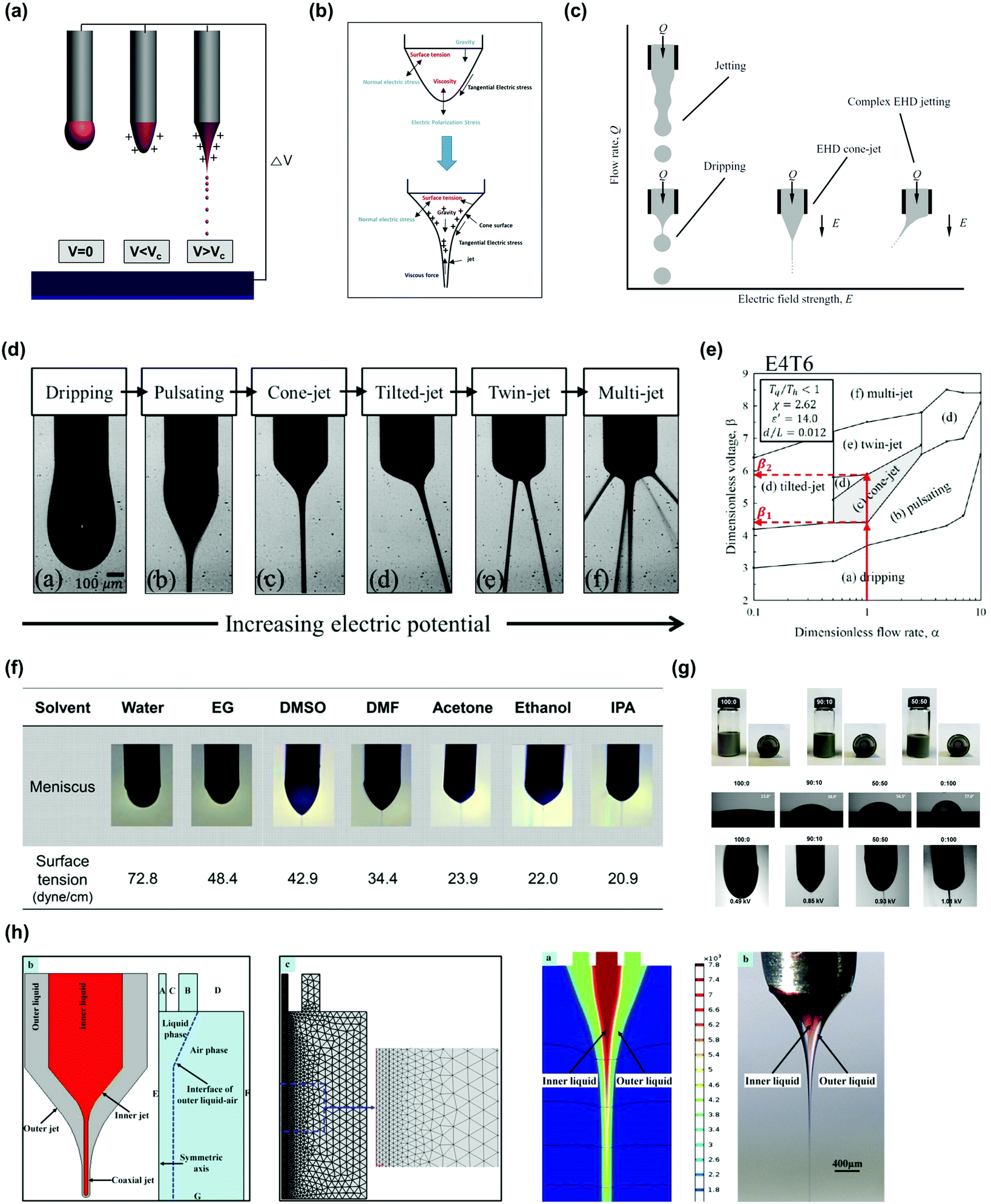 | ||
| Fig. 1 (a) Schematic illustration of EHD jet printing process and (b) forces that influence the jetting behavior of a droplet at a nozzle tip. (c) Effect of electric field and flow rate on jetting mode. Reproduced from ref. 45 with permission from the Cambridge University Press. (d) Images of jetting mode and (e) jetting behavior depending on dimensionless flow rate α and dimensionless voltage β of ethanol and terpineol mixture. Reproduced from ref. 46 with permission from the American Chemical Society. Jetting behaviors according to (f) surface tension and (g) conductivity of ink. Reproduced From ref. 50 and 51 with permission from the Wiley-VCH and the Elsevier. (h) Schematic illustration of simulation system and practical jetting image of EHD jet printing. Reproduced from ref. 56 with permission from the Springer Nature. | ||
This printing concept can be expressed numerically. The droplet generated at the nozzle tip is governed by the electric force FE, surface tension FS, viscous force FV, and gravitational force FG (Fig. 1b).43,44 The formation of the jet can thus be described by the Navier–Stokes equation
| ρ(∂u/∂t + u·∇u) = −∇p + F_V + F_E + F_S + F_G, | (1) |
| ∇·u = 0. | (2) |
| F_G = ρg, | (3) |
| F_V = ∇·T_V = μ∇2u, | (4) |
The surface tension only acts in a direction normal to the interface between the air and liquid, and can be expressed using the Dirac distribution function δS as
| F_S = σκδ_Sn, | (5) |
FE is computed using Maxwell's equations as
| F_E = ∇·T_M = q_VE − 1/2E2∇ε, | (6) |
| q_V = ∇·(εE). | (7) |
Different experimental conditions, such as the electrical field (or applied voltage), can control and produce different jetting behaviors in addition to a stable jetting mode (Fig. 1c and d). When the electric field is absent or small, the liquid flows out of the nozzle under the influence of gravity; a low flow rate corresponds to dripping mode, and a high flow rate corresponds to jetting mode.45 A slight increase in the flow rate, electric field, or both, from that in the dripping mode leads to formation of a pulsating liquid jet, by which streams of distinct droplets are ejected by repeated formation and relaxation of the Taylor cone. This pulsating jetting behavior can be achieved at flow rates lower than the minimum flow rate, or at voltages lower than the critical voltage required for the steady cone-jet mode. A further increase in the voltage above VC leads to a continuous stream of liquid from the nozzle along with the continuous presence of the Taylor cone. This is referred to as the cone-jet mode or stable jetting mode of EHD jet printing. At much higher electric fields than these, complex jetting behaviors such as tilted jets and multiple jets (with two or more jet streams) occur. Therefore, EHD jet printing under a high electric field leads to atomization or a spray mode. In general, the deposition of functional materials is best using either pulsating-jet mode or cone-jet mode.
The jetting behavior can also be altered by other factors, such as the characteristics of the ink. Therefore, several studies have been conducted to take these variables into account. A systematic and quantitative study of various modes of jetting behavior for a given ink and printer setup46 identified 10 key variables related to the characteristics of the ink, the geometry of the system, and to various processing conditions (e.g., density, surface tension, permittivity of free space and the fluid, conductivity, viscosity, nozzle diameter, distance between nozzle tip and substrate, flow rate, and applied voltage) that govern the electrodynamics and fluid dynamics during the EHD jet printing process. These variables were reduced to six dimensionless numbers by using the Buckingham π theorem. During EDH printing using mixtures of ethanol and terpineol, the jetting behavior was classified as a function of the dimensionless voltage β and dimensionless flow rate α (Fig. 1e). This approach allows different injection modes to be described quantitatively, and therefore can provide useful information regarding the selection of process conditions in future studies.
Several studies have also been conducted to confirm the formation of the cone-jet mode while controlling the parameters of the ink.47–49 During EDH printing using two types of polymeric ink (polystyrene (PS) and poly(methyl methacrylate) (PMMA)) with different physical and chemical properties,50 the effect of varying the fluid parameters (i.e., surface tension, viscosity, conductivity, dielectric constant, and molecular weight) were investigated. The surface tension of the various solvents critically determined the properties of the cone-jet mode (Fig. 1f). The viscous properties of the ink also influenced the deposited layers, and the droplet diameter decreased when the polymers had high molecular weight.
In a study that exploited cone-jet mode with a highly-conductive ink composed of Ag nanowire (AgNW), which has conductivity of range 10−13–10−3 S m−1,51 the pristine AgNW ink with high conductivity failed to form the cone-jet mode, but addition of polyethylene oxide (PEO) to the pristine AgNW ink induced a decrease in the conductivity and thereby permitted a stable cone-jet mode during EHD jet printing. PEO has excellent solubility for hydrophilic metallic solutions or inks,52,53 and the insulating properties of PEO can modify the conductivity of metallic ink to facilitate EHD jet printing.
In addition to theoretical modeling and experimental analysis, numerical simulations of the EHD jet formation process have also been performed.54,55 Numerical simulations to find the optimized conditions for coaxial EHD jet printing utilizing a three-phase liquid–liquid–air model (Fig. 1h),56 were used to guide investigation of the effect of various working parameters (e.g., applied voltage, flow rate of the inner coaxial liquid, size of the Taylor cone) on the morphology of the jet. The results agreed well with those of physical experiments. Using optimized working parameters obtained from the simulations, a stable nanoscale jet was formed by the combined effect of the electric shearing force, viscous shearing force, and internal pressure. Subsequently, various patterns with a diameter of 70 nm were printed using this jet.
Numerical simulations that applied the Taylor–Melcher leaky dielectric model of droplet generation during EHD jet printing successfully simulated the droplet generation process in one cycle, including the formation of the Taylor cone, jet onset, jet break, and jet retraction.54 The simulated results agreed well with the corresponding experimental results. Further analysis revealed three constraints that must be considered during EHD jet printing: voltage, flow rate, and nozzle diameter. Research on the formation of jets in EHD jet printing is still in progress.57–59 Understanding of the EHD jet printing process for practical printing applications will likely increased in the near future.
Research on the basic principles and mechanisms behind jet formation has led to the discovery of various materials and printing processes that can be deposited using EHD jet printing. In particular, depending on the purpose of the user with this mechanism, different types of EHD jet printing can be realized, such as pulsating jet or cone-jet mode, EHD spraying mode, and electrostatic-force-assisted dispensing mode.
The most commonly-used printing mode exploits formation of the Taylor cone, and is known as the pulsating-jet or cone-jet mode. Pulsating-jet mode is a micro-dripping mode that exhibits repeated formation of Taylor cones due to the application of a pulsed DC voltage or because of the natural frequency of jet ejection during the printing process (Fig. 2a).60 This natural frequency has been explored from the point of view of electrospray applications and scaling laws to describe for the pulsation frequency have been proposed using the frequency spectrum of capillary waves on the surface of a charged droplet.61
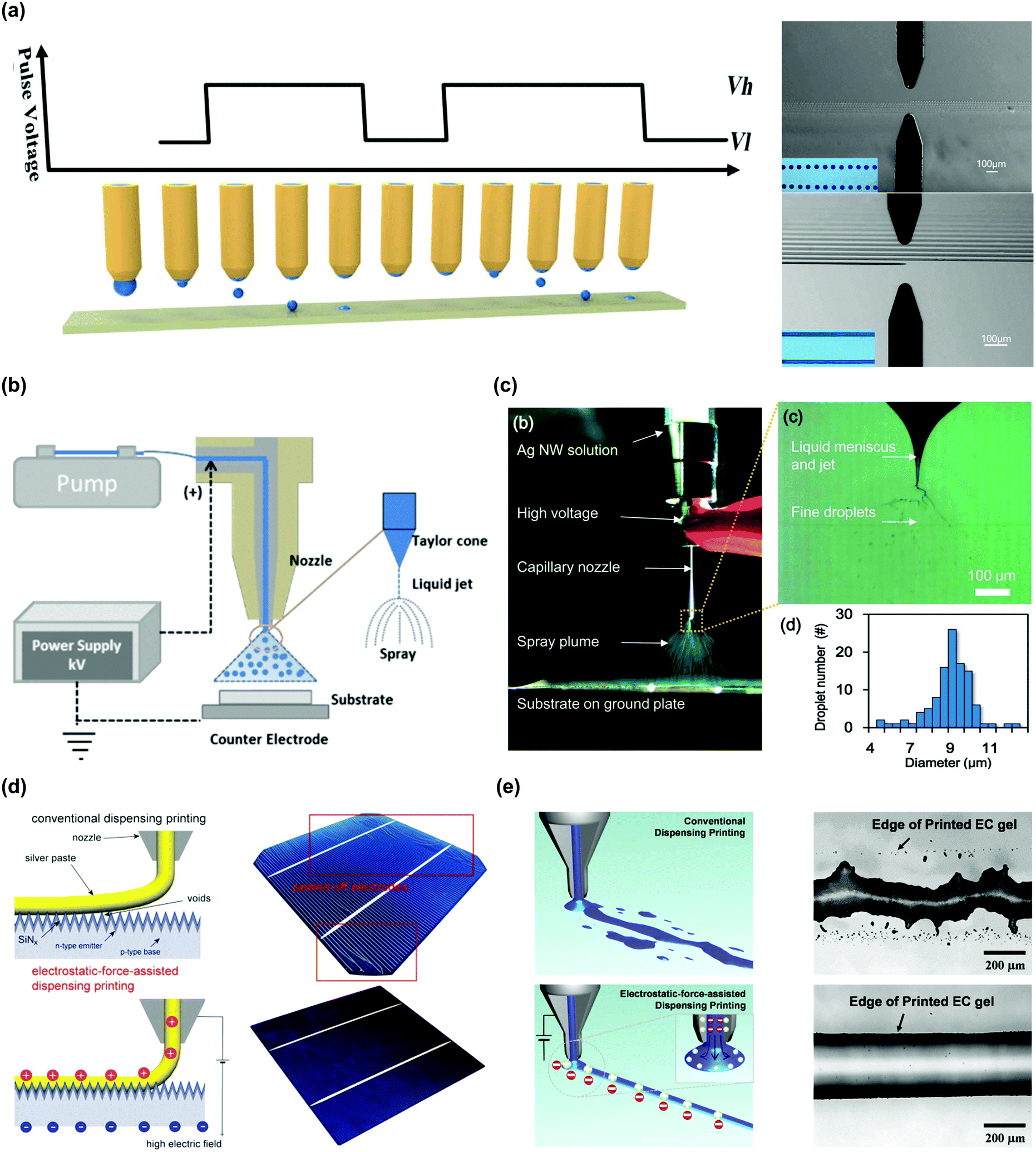 | ||
| Fig. 2 (a) Schematics of pulsating mode and practical printing images of pulsating jet and cone-jet modes. Reproduced from ref. 60 with permission from the IOP Publishing Ltd. (b) Schematics of EHD spraying mode and (c) photograph of detailed EHD spraying mode. Reproduced from ref. 66 and 69 with permission from the American Chemical Society and the Royal Society of Chemistry, respectively. (d) Highly viscous Ag layers printed using electrostatic-force-assisted dispensing mode on rough surface. Reproduced from ref. 72 with permission from the Springer Nature. (e) Electrostatic-force-assisted dispensing mode with ion-gel materials on ITO-patterned glass. Reproduced from ref. 73 with permission from the American Chemical Society. | ||
The electric field affects the frequency and can be described using scaling laws that illustrate the dependence of the pulsations of a liquid jet on the flow rate, jet diameter, and intrinsic pulsation frequency.35 The intrinsic pulsation frequency is proportional to the electric field strength raised to the power of 1.5 on a logarithmic scale. A decrease in the back pressure in the ink supply system resulted in increased pulsation frequencies and reduced droplet sizes.
A pulsed DC voltage printing regime high-speed, high-resolution, and high-precision EHD jet printing,62 uses the duration of the pulse to determine the volume of the droplet and size of the pattern on the substrate. This method has achieved high-speed drop-on-demand printing capabilities at 1 kHz and droplet sizes in the range 3–5 μm (for aqueous ink) and 1–2 μm (for photocurable polymer ink). Therefore, because of its ability to deposit micro- and nanometer-sized droplets, this printing mode is widely used to fabricate finely-patterned functional materials.20,63,64
Cone-jet mode exploits formation of a stable Taylor cone when a continuous voltage is applied. The mode ejects jets of ink continuously from the nozzle. This printing mode is possible only under appropriate printing conditions (e.g., electric field, flow rate, and properties of the ink), but enables high-resolution and high-precision deposition of functional materials in the desired pattern.18,19,65 However, when the printing distance is too long (≥700 μm), the jets decompose into a spray that is emitted from the droplet under the influence of the electric field; hence, precise printing to form a fine pattern is possible only when the printing distance is minimized.
EHD spraying mode develops when the distance between the nozzle and the substrate in the cone-jet mode is large, and jetting behavior changes to a spraying behavior (Fig. 2b).66 Compared to conventional spraying modes, the EHD spraying mode can generate finer droplets without significant agglomeration owing to the repulsive force between the highly-charged droplets or solute particles,67 produce smaller droplets,68 and achieves higher deposition efficiency with a smaller material loss. This spraying mode has been used to deposit patterned AgNW electrode layers for fabrication of flexible organic solar cells (Fig. 2c).69 Their work also confirmed that the EHD spraying mode has the potential to be scaled up for large-scale printing and direct patterning of various types of functional materials.
In contrast, when the distance between the nozzle and the substrate is smaller than the diameter of the droplet at the nozzle tip, the printing is performed in a dragging mode, which is referred to as the electrostatic-force-assisted dispensing mode. This printing mode has properties of both the dispensing and EHD-jet printing methods. As in the EHD jet printing technique, an electric field is applied between the nozzle and the substrate during the dispensing process. Therefore, the charged ions or solutes in the droplet at the nozzle tip create an electrostatic attraction between the substrate and the deposited functional material, and thereby strengthen the adhesion between the two and help increase the density of the printed layers.70,71 This printing mode has been used to deposit highly viscous Ag ink on the surface of a crystalline silicon solar cell (Fig. 2d); and to construct electrodes that had unusually high aspect ratio using single-pass printing.72
Electrostatic-force-assisted dispensing mode has also been used to print electrochromic materials in ion gel.73 In this mode, an electrostatic attraction formed between the ion gel and indium tin oxide (ITO)-patterned glass, so the ion-gel layer is well-defined (Fig. 2e), whereas the conventional dispensing technique formed poorly-adhered films. Thus, EHD jet printing is a useful technique that can be applied in several modes. Different types of functional materials can be printed using these modes and the printed layers can be applied to several types of electronic device.
3. EHD jet printing of functional materials
3.1 Conductive materials
The use of electronic ink (e-ink) is key to implementing EHD jet printing technology to produce electronic devices; therefore, we discuss the features of e-ink in detail in this section. E-ink is considered to be one of the most important components of printed electronics technology and is responsible for determining the final electrical characteristics of the electronic product. These inks can be approximately classified into three categories: (1) metals, such as gold, silver, copper, palladium, and nickel; (2) carbon materials, such as carbon nanotubes (CNTs), graphene, carbon black, and carbon matrix composites; and (3) conductive polymers, such as poly(3,4-ethylenedioxythiophene):polystyrene sulfonate (PEDOT:PSS) and polycaprolactone/poly(acrylic acid) (PCL/PAA).E-ink is characterized by several important physical parameters, such as the zeta potential, viscosity, surface tension, and sintering temperature. These physical parameters directly influence the e-ink's characteristics and possible applications. E-ink is composed of various additives, and its conductivity depends on the conductivity, type, and content of the additives. High-quality conductive ink must satisfy six basic requirements: (1) good stability, to ensure that the components do not easily decompose and agglomerate; (2) good rheological properties, to ensure smooth printing; (3) compatibility with the substrate; (4) low electrical resistance after curing and film-forming; (5) narrow printing line width or high resolution; and (6) low ink-to-conductive film conversion temperature.
The fabrication of low-resistance printed electrodes is the key to improving the electrical characteristics of electronic devices. Metal inks have low resistivity and a small temperature coefficient of resistance (Table 1), so they have become the main material for printed e-ink devices. The resistivity of copper (Cu) is 16.78 nΩ m, and it is abundant and inexpensive, so it is widely used. A Cu electrode can be to directly patterned using a non-contact EHD jet process to print high-resolution Cu wire with a minimum width of 40 μm, by using Cu paste with a viscosity of 4000 cP, with propylene glycol monomethyl ether acetate (PGMEA) as an additive (Fig. 3a and b).74 Cu electrodes annealed in vacuum had better properties than those annealed in air. Annealing in vacuum burned the organic compounds in the copper electrodes, leaving behind a surface that was distinctly different from those of samples annealed in air. Annealing in vacuum also caused coarsening, which made the Cu particles bond together. Zinc tin oxide (ZTO)-based thin-film transistors (TFTs) fabricated with the vacuum-annealed Cu electrodes had good properties, with a field-effect mobility μFET = 0.50 cm2 V−1 s−1, an on/off current ratio Ion/Ioff = 5.5 × 10⁵, and a threshold voltage Vth = 11.9 V. These results show that EHD jet-printed Cu has several potential applications in fabrication of electronic devices.
| Material | Resistivity (×10−8 Ω m) | Temperature coefficient of resistance (°C−1) |
|---|---|---|
| Gold | 2.4 | 0.00324 |
| Silver | 1.586 | 0.0038 |
| Copper | 1.678 | 0.00393 |
| Aluminium | 2.65 | 0.00429 |
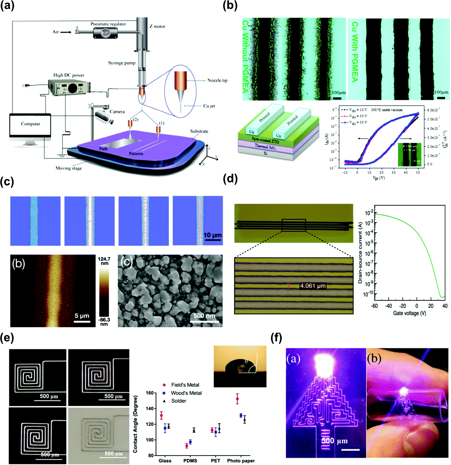 | ||
| Fig. 3 Metallic ink application with EHD jet printing process: (a) schematics for EHD jet printing of Cu electrode, (b) optical microscopic image with EHD jet printed Cu layers and TFT application. Reproduced from ref. 74 with permission from the Wiley-VCH. (c) EHD printed Ag electrodes characteristics and (d) application as OTFT electrodes. Reproduced from ref. 80 with permission from the Royal Society of Chemistry. (e) Field's metal electrode patterns with EHD jet printing and (f) touch sensor connected to a light-emitting device. Reproduced from ref. 82 with permission from the Wiley-VCH. | ||
Cu is easily oxidized in air, especially at the nanoscale, where its specific surface area is high.75 Copper oxide has much higher resistivity = 5.1 × 10⁸ nΩ m than Cu (17.2 nΩ m) and it almost behaves like an insulator. Similarly, the resistivity of silver (Ag) is 15.9 nΩ m, whereas silver oxide has a low conductivity. However, Ag is relatively more difficult to oxidize than Cu, and is therefore regarded as the most promising material for preparing highly conductive and stable inks; moreover, Ag is the most studied e-ink material for inkjet printing.76,77 Recent developments in flexible printing technology and nanotechnology for high-resolution electronic components have directed attention to different types of Ag nanostructures.78,79
Top-contact organic thin-film transistors (OTFTs) have been fabricated using direct EHD jet-printed Ag electrodes with a channel length of 5 μm (Fig. 3c).80 Ag nanoparticles were doped with 2,3,4,5-tetrafluoro-7,7,8,8-tetracyanoquinodimethane (F4-TCNQ) by using a solution processing method. The OTFTs with printed electrodes had electrical characteristics comparable to those of devices composed of top electrodes prepared using thermal evaporation. An OTFT with a channel current in the milliampere range, channel length of 4 μm, and width![[thin space (1/6-em)]](https://www.rsc.org/images/entities/char_2009.gif) :length ratio >300 was demonstrated (Fig. 3d). The printing process used was highly repeatable and the difference between individual devices was very small, so the OTFTs achieved a high current output.
:length ratio >300 was demonstrated (Fig. 3d). The printing process used was highly repeatable and the difference between individual devices was very small, so the OTFTs achieved a high current output.
EHD jet printing technology can directly print AgNWs on various flexible substrates.81 The printed AgNW patterns had a low resistivity (as low as 175 nΩ m). In addition, fabricated flexible heaters showed a uniform temperature distribution with a maximum heating rate of ∼21 °C s−1 and a maximum cooling rate of ∼29 °C s−1.
Low-melting-point metal ink (e.g., Field's metal) is also commonly used in EHD jet printing. It has been used to directly manufacture metal wires using EHD jet printing with a resolution of <50 μm (Fig. 3e).82 The electrical response was stable after several hundred bending cycles and during the stretching/releasing cycles for a wide range of tensile strains (0–70%). The printed metallic conductors had self-healing abilities, such that the faults in the device could be easily repaired by low-temperature heat treatment without affecting their tensile properties. A high-density touch sensor array was also successfully fabricated and tested using these printed conductors (Fig. 3f).
Carbon-based materials are quite abundant and their price has also declined compared to those of metallic inks. CNTs are quite narrow and have smaller inner diameter (∼1 nm) than their outer diameter (several to tens of nanometers). Their lengths are generally on the order of micrometers, and their ratio of length to diameter is very large, approximately 103–106. CNTs are excellent one-dimensional media, which have very high mechanical strength, and tolerance of elastic strain up to 12%.83 However, owing to the strong van der Waals force, CNTs do not readily disperse in solvents; hence, development of a stable dispersion is a prerequisite for the preparation of CNT inks for EHD jet printing of electrodes. Three dispersants; i.e., Triton X-100 (TX100), poly(4-styrene-sulfonic acid) (PSS), and sodium dodecylbenzenesulfonate (NaDDBS)), all disperse the multiwalled CNTs adequately (Fig. 4a).48 The nature of the dispersants affected the surface potential and charge-carrier injection properties of CNT composite electrodes printed using EHD jet printing. The printed MWCNT/PSS lines showed excellent electrical characteristics when used as electrodes in p-type OTFTs (Fig. 4b), whereas MWCNT/TX100 lines showed excellent electrical properties when used as electrodes in n-type OTFTs (Fig. 4c).
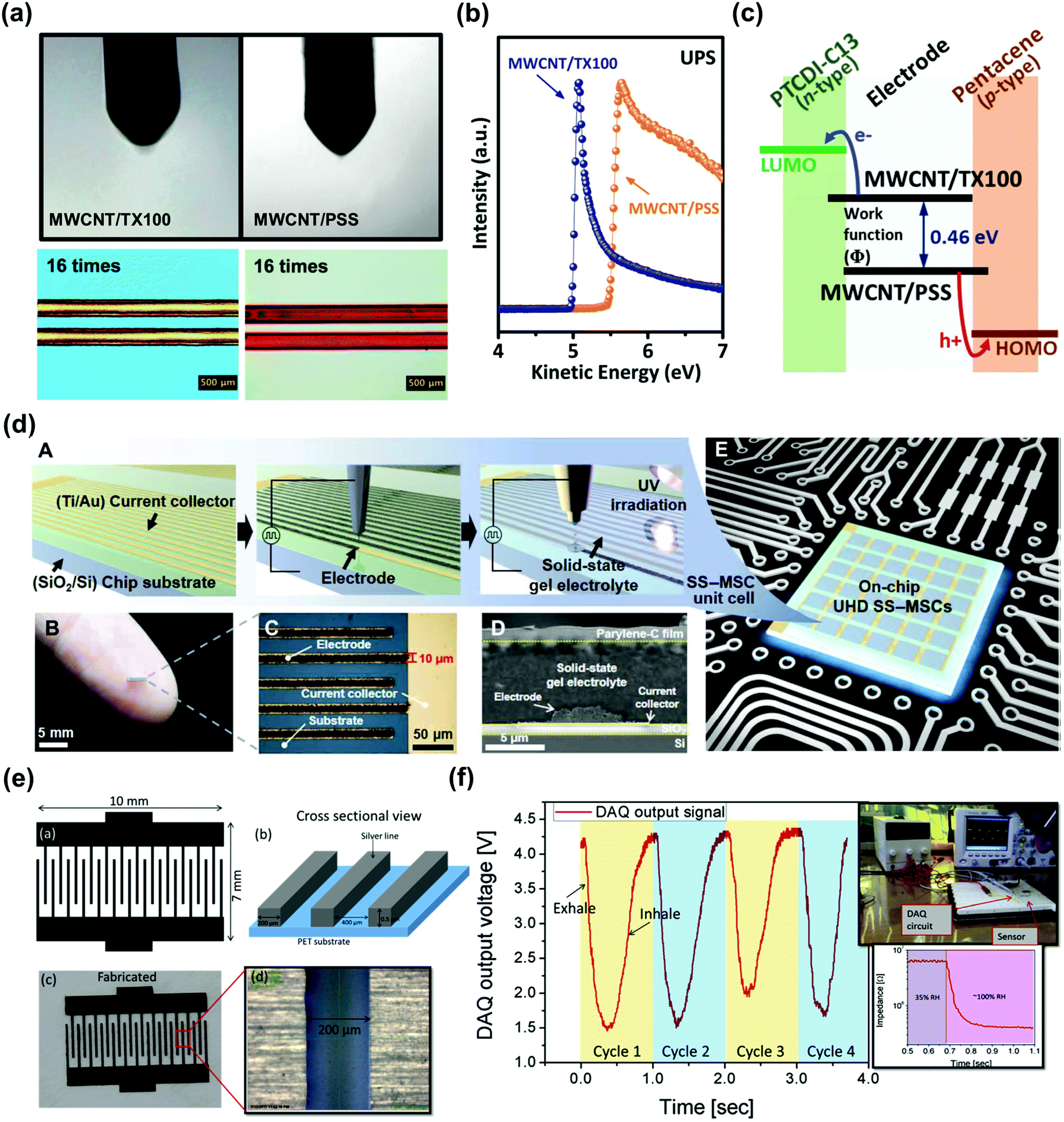 | ||
| Fig. 4 Carbon-based electronic materials obtained by EHD jet printing: (a) EHD jetting behavior of MWCNT with dispersants, (b) surface potential and (c) charge transport characteristics with these electrodes. Reproduced from ref. 48 with permission from the PCCP Owner Societies. (d) Fabrication of on-chip UHD solid-state microsupercapacitors by EHD jet printing of carbon-based electrodes. Reproduced from ref. 84 with permission from the AAAS. (e) EHD jet printed graphene/methyl-red composite electrodes and (f) humidity-sensing properties. Reproduced from ref. 85 with permission from the Elsevier. | ||
Micro-supercapacitors have been prepared using EHD jet printing of carbon materials, with carboxymethyl cellulose (CMC) as an electrode adhesive to adjust the surface charge of the electrodes.84 The voltage applied in the cone-jet mode was 0.42–0.44 kV and the electrode width was ∼10 μm (Fig. 4d). The electrode width remained almost unchanged during the experiments with only an increase in the number of printed layers.
Methyl-red/graphene composite films of thickness ∼300 nm have been deposited on silver electrodes by using EHD jet printing (Fig. 4e).85 These composite electrodes were used in humidity sensors. The electrical resistance of the sensors varied inversely with relative humidity from 11 MΩ at relative humidity (RH) = 5% to 0.4 MΩ at RH = 95% (Fig. 4f). For capacitive sensors, the capacitance varied from 2.3 pF at RH = 0% to 66 nF at RH = 100%. The response and recovery times were for 0.251 s at RH = 35% and 0.35 s at RH = 100%. The sensor had a resistive sensitivity of 96.36% and a capacitive sensitivity of 2869500%. Such a high-sensitivity sensor could be realized owing to the deposition of methyl-red/graphene composite film on silver electrodes.
Organic polymers have several advantages. They are flexible, recyclable, highly scalable, environmentally benign, and light weight. Numerous types are available, and they allow low-cost and simple device manufacturing, and have excellent solution processability.86 Due to their wide range of optical, mechanical, and electrical properties, hybrid nanocomposites have been used in a variety of electronic devices, including solar cells, memristors, sensors, thin-film transistors, and light-emitting diodes.87–89 PEDOT:PSS is one of the most important conductive polymers; it has excellent chemical and physical properties, such as high conductivity, optical transparency, water solubility, good film-forming ability, and mechanical flexibility, and is therefore an important material from the perspective of both practical applications and basic research.90,91
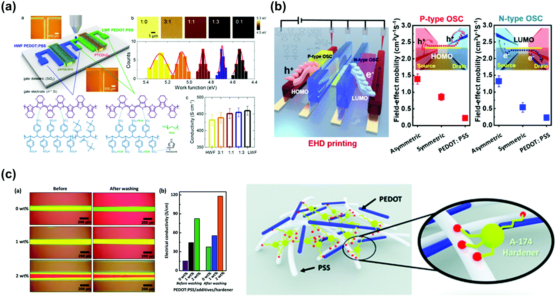
After tuning of the work function of EHD jet-printed PEDOT:PSS electrodes (Fig. 5a) they were used to manufacture OTFTs that had efficient charge transport, and complementary logic circuits.90 Two types of PEDOT:PSS materials, one with a high work function (5.28 eV) and the other with a low work function (4.53 eV), were printed using EHD jet printing, and applied as the source and drain electrodes of OTFTs, and in complementary logic circuits. OTFTs fabricated using these PEDOT:PSS electrodes with tuned work function had excellent electrical properties, including an Ion/Ioff > 107 and a μFET > 1 cm2 V−1 s−1. The proposed method is excellent for the development of next-generation integrated circuits and other multifunctional electronic devices.
 | ||
| Fig. 5 Polymer-based electronic materials application with EHD jet printing process: (a) work function tuned PEDOG:PSS electrodes produced using EHD jet printing. Reproduced from ref. 90 with permission from the American Chemical Society. (b) EHD jet printed PEDOT:PSS with tunable work function, with specific additives and applied asymmetric electrode structured electronics. Reproduced from ref. 92 with permission from the American Chemical Society. (c) EHD jet printed PEDOT:PSS with silicon hardener and electrical conductivity. Reproduced from ref. 93 with permission from the PCCP Owner Societies. | ||
The work function of PEDOT:PSS was tuned by addition of fluorine- and amine-based additives, then used to print asymmetric electrodes to enhance the charge injection/extraction characteristics of OTFTs (Fig. 5b).92 As a result of the difference in the surface energy, addition of fluorine- and amine-based additives led to vertical phase separation after the completion of the EHD jet printing process. Consequently, the surface dipolar effect of the fluorine-based (electron-withdrawing) and amine-based (electron-donating) additives modified the surface potential. Therefore, OTFTs fabricated with these asymmetrically arranged, PEDOT:PSS electrodes had tunable work function had superior charge-transport characteristics (both injection and extraction) between the electrode and the semiconductor, with a μFET > 1 cm2 V−1 s−1 for both n-type and p-type OTFTs.
Additionally, EHD jet printing can use PEDOT:PSS in combination with a hardener to increase the solvent resistance and electrical characteristics (Fig. 5c).93 Addition of a silicon-based hardener to PEDOT:PSS yielded solvent-resistant PEDOT:PSS composites, which when EHD jet-printed had increased electrical conductivity and solvent resistance, and showed efficient charge injection when semiconductor materials were coated onto PEDOT:PSS composite electrodes. When EHD jet-printed PEDOT:PSS composite electrodes were used in OTFTs, they had superior electrical characteristics compared to OTFTs composed of electrodes that had been fabricated without a hardener. Numerous other EHD jet-printed electrode materials have been presented in the literature.40,51,53,90,94–102
3.2 Semiconducting materials
Different types of electronic devices have been developed for switching, sensing, energy harvesting, and display applications, so significant efforts have been devoted to developing and utilizing both organic and inorganic semiconductors for electronic applications. However, some semiconductors that have sufficient charge transport or unique optical properties can be damaged by the processing required for device fabrication. Semiconducting materials with low temperatures of degradation and melting also require low deposition temperatures. In addition, the high thermal and chemical sensitivities of certain semiconductors prevent their manipulation using the fabrication methods used in semiconductor industry. However, they are amenable to direct printing technology, which enables their use in fabrication of electronic devices. EHD jet printing technology allows semiconductors to be printed with a narrow line width and to be applied to complex and integrated devices.Metal oxide semiconductors with high mobilities and transparency can be formed into thin films by using low-temperature solution processing.103–105 Zinc oxide is a representative solution-processable metal oxide semiconductor that can transport electron charge carriers.106–108 To improve its charge-carrier transport characteristics and stability, attempts have been made to dope it with tri- or tetravalent metal atoms, such as tin, indium, and gallium.109–111 The first application of EHD jet printing technology to direct patterning of oxide semiconductors used indium zinc oxide (IZO),112 which was line-printed with line widths of 1.5 and 5 μm on SiO2/Si substrates (Fig. 6a). The IZO ink was composed of the metal salts indium nitrate hydrate and zinc acetate dihydrate, and organic solvents. The composition and annealing temperature of the IZO ink were optimized by spin-coating it onto fabricated TFTs. The same optimized condition that were used to fabricate spin-coated IZO-based TFTs were also used to EHD-print TFT devices with line-patterned IZO that had line width <20 μm (Fig. 6b). The resulting TFTs showed promising electronic characteristics with a μFET = 3.7 cm2 V−1 s−1 and an Ion/Ioff > 105 (Fig. 6c). IZO-based TFTs fabricated in a device configuration of glass (substrate)/indium tin oxide (ITO, gate electrode)/hafnium oxide (HfO2, dielectric)/ITO (source and drain electrodes) had a μFET = 32 cm2 V−1 s−1 and an Ion/Ioff = 103.
 | ||
| Fig. 6 EHD jet printing for patterning oxide semiconductors. (a) Optical microscope (OM) image of line patterns formed by EHD-jet printing of IZO semiconductor precursor solutions, (b) scheme and SEM image of IZO-based TFT structures, and (c) electrical characteristics of EHD-printed TFTs, reproduced from ref. 112 with permission from the AIP Publishing; (d) OM images of ZnA solution at the edge of nozzle tip showing six different modes of EHD printing, and (e) operating modes of the EHD printing according to applied voltage and working distance, reproduced from ref. 116 with permission from the Elsevier; and (f) a scheme of the EHD printing process for patterned ZnO nanorods, and (g–i) sectional SEM images of patterned ZnO nanorods with different line spacing, reproduced from ref. 117 with permission from IOP Publishing Ltd. The line spacing is (g) 10 μm, (h) 20 μm, and (i) 30 μm. | ||
EHD jet printing has been used to prepare indium gallium zinc oxide (IGZO) with a line width of 30 μm, which were then used to fabricate TFTs.113 Use of formamide (FA) solvent in the IGZO precursor solution facilitated EHD jet printing by retarding nozzle clogging. The FA solvent also reduced the content of hydroxide and enabled the formation of oxygen vacancies, thereby improving the overall electrical characteristics of the devices. The EHD jet-printed IGZO-based TFTs had a μFET = 1.3 cm2 V−1 s−1 and an Ion/Ioff = 4 × 10⁶.
EHD printing has also been used to patterned ZTO semiconductors with a line width of 60 μm, for use in TFTs.114 They had a μFET = 9.82 cm2 V−1 s−1 and an Ion/Ioff = 3.7 × 10⁶. EHD jet-printed ZTO had a μFET that was almost three times higher than that of the spin-coated ZTO. The EHD jet-printed TFTs also showed reduced hysteresis and better positive bias stability than TFTs that had been fabricated using spin coating.
EHD jet spraying has been used to fabricate ZTO-based TFTs.115 The spray pattern of ZTO was optimized by modulating voltage applied to the nozzle tip, substrate temperature, solution concentration, pressure in the syringe, and distance between the nozzle and the substrate. The droplets of ZTO deposited had an average diameter of 60 μm. ZTO-based TFTs fabricated using this technique had an electron μFET = 4.89 cm2 V−1 s−1 and an Ion/Ioff = 107.
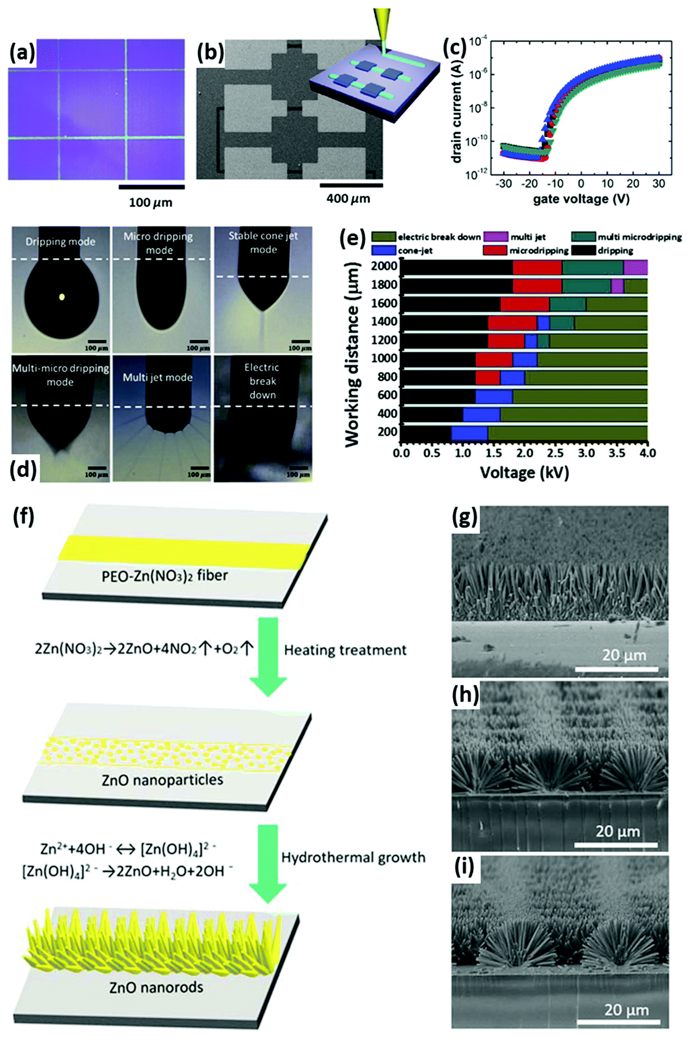
EHD jet printing has been used to print ZnO semiconductors and various solution-processable electrode materials on Si/SiO2 substrates.116 Zinc acrylate (ZnA) was used as the ZnO precursor, and by modulating the printing distance and the voltage applied between the nozzle and the substrate, six different jetting modes were obtained: dripping, micro-dripping, multi-microdripping, cone-jet, multi-jet, and electric break down (Fig. 6d and e). Line-patterned ZnO and ZnO/In TFTs with line widths of ∼100 μm were optimized by varying the solution concentrations and Zn:In precursor ratios. PEDOT:PSS, Ag, and MWCNTs:PSS inks were evaluated to replace thermally-deposited Al electrodes; the MWCNT:PSS electrodes had the best TFT characteristics, with an average μFET = 1.14 cm2 V−1 s−1 and an Ion/Ioff = 8.2 × 10⁵ in TFTs composed of ZnO:In semiconductor and MWCNT:PSS electrodes.
ZnO nanorods have high electron mobility and catalytic efficiency, so they also constitute a promising material to improve the electrical characteristics of ZnO-based functional devices. ZnO have been patterned by using EHD jet printing polyethylene oxide (PEO)–Zn(NO3)2 composite filaments, then heating the substrate to decompose PEO–Zn(NO3)2 to ZnO nanorods (Fig. 6f).117 Decrease in working voltage and increase in printing distance reduced the thickness of PEO–Zn(NO3)2 filaments to a line width of 2 μm, then they were decomposed to ZnO nanoparticles to serve as seed templates for hydrothermal growth of ZnO nanorods. The width of the ZnO nanorods gradually increased to 38 μm as the ZnO nanoparticles grew to form ZnO nanorods (Fig. 6g–i). The photoelectrochemical properties of the patterned ZnO nanorods were well controlled and they showed higher photoelectrochemical stability than spin-coated ZnO nanorods.
EHD jet printing technology enables facile and direct printing of metal oxide semiconductors with high resolution, so this technology has been used to fabricate transistor arrays and integrated circuits.118 In2O3 was used because of its high mobility and low processing temperature. In2O3 patterns with a narrow line width of 2 μm and low thickness of 20 nm were obtained. The TFTs fabricated using these line-patterned In2O3 had a μFET = 7.7 cm2 V−1 s−1 and an Ion/Ioff = 108. When the In2O3 channel layer with a length of 110 μm was EHD jet-printed on Zr-doped AlOx (ZAO), which has a high dielectric constant k, the TFTs had a high electron μFET = 230 cm2 V−1 s−1 and an Ion/Ioff = 103. The fabrication of TFTs that had good electrical characteristics, the improvement in device stability by printing passivation layers, and the desired operation of logic circuits that used EHD jet-printed TFTs demonstrate the versatility of EHD jet printing technology. Successful fabrication of TFTs on plastic substrates also suggests that EHD jet-printed In2O3 is a promising material for use in printed electronics.
In2O3 and IGZO have also been used in all-metal-oxide TFTs, with direct-printed metal oxide TFT with In2O3 or IGZO as the semiconductor, ITO as the electrodes, and Al2O3 as the high-k gate dielectric.40 The channel length of the metal oxide semiconductor layer was 7 μm. The all-printed TFTs had excellent electrical characteristics at a low operating voltage of 2 V, with an average electron μFET = 117 cm2 V−1 s−1 and an Ion/Ioff = >106. Integrated logic gates, such as NOT and NAND, were also fabricated.
Various gases react with the surfaces of metal oxide semiconductors, so they can be used to detectors those gases. Metal-oxide gas sensors with metal oxide nanofibers have been produced using EHD jet printing,119 with nanofibers of SnO2, In2O3, WO3, and NiO as inks. Optimized printing parameters yielded microscale patterns of metal oxide nanofibers with diameters <100 μm. Gas sensors have also been fabricated using the EHD printing technique on microelectrodes to detect toxic gases, such as NO2, CO, and H2S. These four metal oxides could detect concentrations as low as 0.1 ppm of NO2, 20 ppm of CO, and 1 ppm of H2S.
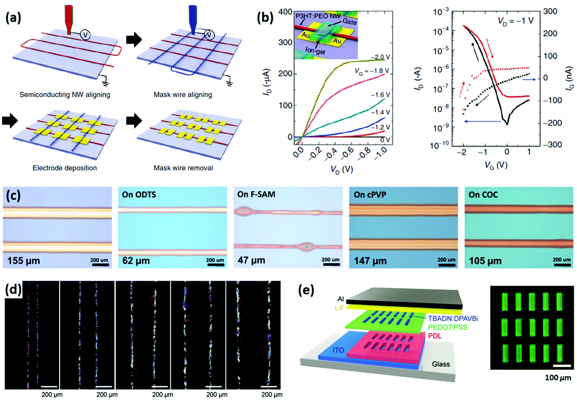
Organic semiconductors (OSCs) are representative solution-processable materials used in printed electronics.120–122 OSCs enable facile and direct printing at low temperature, so they can be printed on various substrates, including plastics, to fabricate flexible devices. The first report of EHD jet printing of an organic semiconductor used poly(3-hexylthiophene-2,5-diyl) (P3HT) and poly((N,N′-bis(2-octyldodecyl)naphthalene-1,4,5,8-bis(dicarboximide)-2,6-diyl)-alt-5,5′-(2,2′-bithiophene)) (N2200) to fabricate p-type and n-type organic semiconductors, respectively.37 The viscosity range that is suitable to yield a stable EHD printing mode is wider for conductive materials than for insulating materials, so poly(ethylene oxide) (PEO) was added to the semiconductor solutions to increase their viscosity. The two semiconductors were printed as nanowires that had radius <780 nm. The source and drain electrodes were patterned by introducing a nanoscale electrode gap using EHD jet-printed polymer nanowires (Fig. 7a). When a high-capacitance ion-gel polyelectrolyte was used as the gate dielectric material (Fig. 7b), the resulting P3HT-based nano-channel TFTs had a high hole μFET up to 9.7 cm2 V−1 s−1. Use of line-patterned P3HT to fabricate ion-gel polyelectrolyte nanogap transistors yielded a high μFET, but TFTs with a device configuration of Si/SiO2/P3HT/Au had a μFET = 0.015 cm2 V−1 s−1 because of the PEO insulator in the P3HT solution.
 | ||
| Fig. 7 EHD jet printing as a route to electronic devices based on organic semiconductors. Printing of organic semiconductor printing (a) schematic illustration of the process to fabricate nano-channel TFTs using EHD printing technology, and (b) electronic characteristics of nano-channel TFTs with ion-gel polyelectrolyte, reproduced from ref. 37 with permission from the Springer Nature; (c) OM images of EHD-printed P3HT lines on various surface treated substrates, reproduced from ref. 123 with permission from the American Chemical Society; (d) polarized-OM images of line-printed TIPS-pentacene crystals with various line width, reproduced from ref. 132 with permission from the American Chemical Society; and (e) a scheme of OLED structures with EHD-printed small-molecule pixels, reproduced from ref. 133 with permission from the Royal Society of Chemistry. The right figure is fluorescence-OM image of OLED pixel arrays. | ||
The increased viscosity in the solutions with PEO can lead to nozzle clogging during the EHD jet-printing process. This problem can be solved by modifying the dielectric surface and printing P3HT lines without any polymer binder, and controlling the SiO2 dielectric layer by introducing self-assembled monolayers and polymer thin films.123 The width of the P3HT lines decreased as the surface energy decreased and as the surface wettability of P3HT decreased on hydrophobic surfaces (Fig. 7c). Therefore, the line-patterned P3HT on octadecyltrichlorosilane-modified substrates had the narrowest line width of 100 μm and the highest hole μFET = 0.045 cm2 V−1 s−1, with an Ion/Ioff = 2.1 × 10⁴.
Semiconducting polymers with diketopyrrolopyrrole (DPP) moieties have also been patterned using the EHD jet printing technology for use in TFTs. These polymers have been extensively developed and used in TFTs owing to their rigid and planar structure, strong intermolecular interactions, and resulting crystalline structures.124–126 One such polymer yielded a high μFET and ambipolar charge transport characteristics.127 EHD jet printing of the polymer ODTS-treated Si/SiO2 substrates yielded line patterns with a line width <26 μm. Films produced using EHD jet printing films had moderate surface roughness and a homogeneous crystalline morphology with only the edge-on crystal orientation, whereas the spin-coated films had high surface roughness and mixed crystal orientation. Therefore, the EHD jet-printed TFTs had high hole μFET = 0.75 cm2 V−1 s−1 and electron μFET = 1.08 cm2 V−1 s−1.
To improve the solubility of DPP-bearing polymers for facile and stable EHD-printing, new versions were obtained by replacing some sulfur atoms with selenium atoms in the thienothiophene units.128 This replacement leads to a minimal change in the planarity of the polymer backbone, and can improve the solubility of polymer, but maintains the high crystalline ordering of the polymer chains. Moreover, silicon substitution at the branching position causes volumetric extension of the alkyl side chain, and increases the solubility of DPP-bearing polymers. Consequently, stable jetting conditions and highly uniform electrical characteristics of the polymer-based TFTs were obtained. The resulting TFTs with polymer patterns <25 μm yielded a maximum hole μFET = 3.07 cm2 V−1 s−1. Polymer-based TFTs are operationally stable, so they have been used in ammonia-gas sensors.
Small-molecule semiconductors with strong intermolecular interactions can yield efficient charge transport characteristics in electronic devices.129–131 6,13-Bis(triisopropylsilylethynyl) pentacene (TIPS-pentacene) is a stable and solution-processable small molecule that has been extensively used in electronic devices. TIPS-pentacene has been printed using an EHD jet printer.132 To provide good charge-transport properties, small-molecule semiconductors require optimal molecular packing, so TIPS-pentacene was printed using the dragging mode, which provides a favorable environment for the growth of TIPS-pentacene. When the line width was varied from 150 to 400 μm, all line patterns had good crystalline morphologies (Fig. 7d), so in TFTs fabricated using them had a high hole μFET = 1.65 cm2 V−1 s−1.
EHD jet printing technology has also been used to fabricate organic light-emitting diodes (OLEDs). Small-molecule pixels with high resolution and size of 5 μm gave finer resolution than pixels obtained using conventional inkjet printers, or of pixels found in commercial OLED displays.133 The thickness of the EHD jet-printed pixels, which is one of the most important factors that affect the OLED efficiency, was modulated by adjusting the ink composition and printing speed. The resulting films had a uniform and flawless surface, and OLEDs composed of EHD jet-printed pixels (Fig. 7e) had an external quantum efficiency of 4.6%.
Low-dimensional materials, such as nanoplates, nanowires, and nanoparticles, have unique optoelectronic characteristics such as quantum confinement, due to their nanoscale structure. These materials can be dispersed in organic solvents and used as dispersion inks for various optical and electronic applications. The first printed two-dimensional materials with high resolution134 formed reduced graphene oxide (RGO) dispersion inks into lines of width 5 μm and thickness 8 nm by consecutively printing eight times. The thickness of the printed lines was increased to ∼50 nm by repeating the printing 90 times. The RGO inks were successfully printed even on highly curved surfaces with radius of curvature 50–65 μm. When all-printed RGO-based TFTs were fabricated, the RGO inks were line-printed in the channel area of the TFTs, and yielded a hole μFET = 6 cm2 V−1 s−1.
Transition metal dichalcogenides (TMDs), such as molybdenum disulfide (MoS2), are another class of two-dimensional materials. MoS2 offers a high μFET and a 1.8 eV bandgap, which is advantageous for suppressing the source-to-drain tunneling in short-channel TFTs.135–137 MoS2 has been printed using EHD jet printing to fabricate gas sensors.138 The MoS2 inks were obtained by exfoliating bulk MoS2 to flakes that had only a few layers, then dispersing the flakes in isopropyl alcohol. The MoS2 ink was printed using stable multi-jet mode, and the density of the MoS2 flakes deposited on the substrate was controlled by modulating the printing time. The result was a highly-uniform MoS2 thin film. Gas sensors that used MoS2 as the chemoresistive gas sensing material detected NO2 at concentrations as low as 100 ppm at 100 °C, and had highly reproducible NH3-sensing behavior over repeated sensing cycles when exposed to 100 ppm NH3.
The efficiency of exfoliation of two-dimensional materials can be increased, and the concentration of the ink can be increased by soaking the bulk powders in various solvents for 5 min to facilitate exfoliation.139 During soaking, the d-spacing of the bulk powders increases slightly owing to the different dielectric environment of the solvent. Thus, water-soaked MoS2 and WS2 inks with increased concentrations were obtained. The inks were patterned using EHD jet printing to achieve a lines with widths of 300–400 μm, which were then used as photoactive materials in photodetectors. The resulting devices could detect as little as 0.05 sun irradiation.
EHD can also be used to print MoS2. A (NH4)2MoS4 precursor solution was applied in cone-jet mode, then annealed to form MoS2.140 The atomic layers of the printed MoS2 were tailored by controlling the concentration of the precursor solution. MoS2 line patterns with a resolution of 150 μm and high uniformity were used as the semiconductor layer in TFTs, resulting in a high μFET = 19.4 cm2 V−1 s−1. The electrical characteristics of MoS2-based TFTs were improved using a high-k dielectric.141 The EHD jet-printed MoS2 was coated onto Si/Al2O3 substrates and used as the semiconductor layer in TFTs. The corresponding MoS2 TFT had an average linear μFET = 47.64 cm2 V−1 s−1.
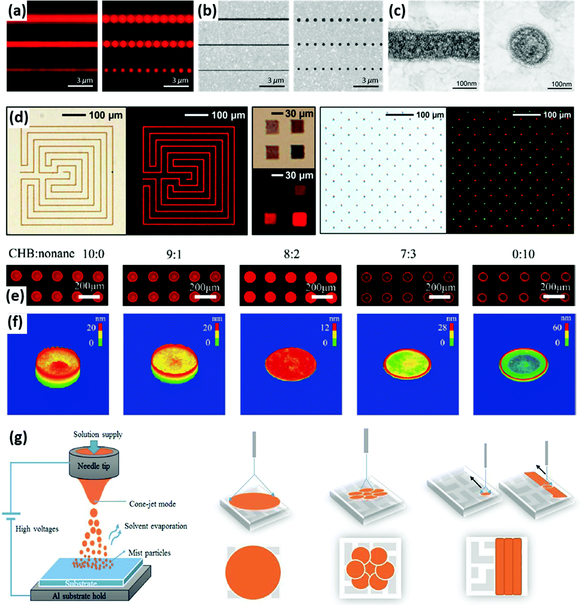
Colloidal quantum dots (CQDs) have attracted considerable interest as light-emitting materials because of their facile color tunability, high color purity, and high quantum efficiency.142–144 Once their surfaces are passivated using organic ligands, CQDs become suitable for use in printing processes. The first report of EHD jet printing of CdSe/ZnS and CdSe/CdsS CQDs on flat and structured substrates used nanodrip mode.145 The EHD NanoDrip printing enabled high-resolution patterning of CQDs with a line width of 100 nm and good film qualities similar to those obtained using spin- and dip-coating. Fluorescent lines of widths 220, 150, and 100 nm were obtained by varying the voltage-pulse parameters and number of overprints (Fig. 8a and b). A countable number of individual CQDs was arranged within a densely packed layer in line and dot patterns (Fig. 8c). High-resolution spots of 30 nm were obtained by diluting the ink, translating the piezo-stage quickly at 200 μm s−1, and using a relatively low ejection voltage (150 V). Hybrid quantum-dot-plasmonic circuits that generate, guide, and decouple surface plasmon polaritons were also fabricated; in these circuits, quantum dots act as local plasmonic sources under far-field illumination with ultraviolet light.
 | ||
| Fig. 8 EHD jet printing methods to print quantum dots and printed patterns: (a) fluorescence microscope images, (b) SEM images, and (c) and high-resolution SEM images of CQDs patterned using EHD jet printing technology, reproduced from ref. 145 with permission from the American Chemical Society; (d) EHD-printed CQDs in various geometries reproduced from ref. 63 with permission from the American Chemical Society; (e) fluorescence microscope images and (f) 3D morphology images of CQD arrays printed using different inks, reproduced from ref. 146 with permission from the Wiley-VCH; (g) schematic illustration of EHD jet spraying modes of a big-circular thin film, a spiral lune, and a straight-line method (from left to right), reproduced from ref. 147 with permission from the Springer Nature. | ||
CdSe CQDs have also been fabricated using EHD jet printing.63 The pattern and thickness of the CQDs were controlled at high resolution by adjusting the operating conditions, such as the dimension of the printing nozzle and the composition of the ink (Fig. 3d). In the pulsating jet mode, EHD drop-on-demand printing yielded arrays of circular deposits of QDs with a diameter of ∼3.9 μm. Direct patterning and stacking of CQDs by EHD jet printing led to formation of homogeneous arrays of patterned CQDs. Light-emitting diodes (LEDs) fabricated using these CQD arrays achieved an external quantum efficiency of 2.6%.
Controlling the properties of LED pixels to achieve a uniform thickness and homogeneous morphology is extremely important for the fabrication of LEDs. Precise control of the capillary flow, which is driven by the concentration gradient, and of the Maragoni flow, which is driven by the surface tension gradient, is necessary to avoid the coffee-ring effect, which is commonly observed during the printing process.
A mixed-solvent method can be used to pattern high-quality LED pixels at high resolution by using EHD jet technology.146 A solvent containing a mixture of cyclohexylbenzene and nonane in a volume ratio of 4:1 was used to print CdSe-based CQDs. Cyclohexylbenzene, which has a high boiling point, was chosen as the main solvent, and nonane, which has low surface tension, low viscosity, and low toxicity, was mixed to solve the coffee-ring problem. The precise modulation of the droplet volume and printing parameters resulted in a high-resolution CQD matrix with a CQD diameter of 1 μm (Fig. 8e and f). Owing to the formation of a uniform CQD film in each pixel, the pixelated LEDs were operated at a low turn-on voltage of 3 V and exhibited a maximum luminance of 8533 cd m−2 at a voltage of 9 V.
EHD jet spraying technique can generate CdSe-based CQDs, which can then be used to fabricate LEDs.147 Circular, spiral lune, and straight-line EHD spraying methods were used to tailor the morphology of the CQD thin films as (Fig. 8g). Among these three, the straight-line spraying method is considered as the most promising method for forming large-scale uniform films. Moreover, LEDs fabricated using the straight-line spraying method exhibited the best electrical characteristics, with a low turn-on voltage of 3.0 V, luminance of 7801 cd m−2 and maximum current efficiency of 2.93 cd A−1. CdSe-based CQD ink composed of a mixture of n-hexane in n-butanol solvent applied using EHD jet spraying achieved improved LEDs that had maximum luminance of 12082 cd m−2 and maximum current efficiency of nearly 4.0 cd A−1.148
EHD jet printing technology can pattern PbS CQDs and fabricate infrared photodetectors.149 The devices used circular pillars of CQDs on thin films of graphene. Application of an alternating electric field deformed the ink meniscus at the nozzle and induced subsequent drop-on-demand ejection of attoliter-sized droplets by continuous break-off. The dimensions of the printed features were drastically reduced due to the small droplet size, fast evaporation of the ink solvent on the substrate, and electrostatic autofocusing of subsequent droplets. Therefore, highly homogeneous CQD films with pillar diameter <1 μm were formed. The resulting phototransistors constructed using these ultra-thin PbS/graphene films as the active layers had high responsivity >104 A W−1, which increased when the thickness of the CQD film was changed to 130 nm.
Perovskite quantum dots (PQDs) are a class of light-emitting materials that have emission colors that can be tuned over the entire visible spectrum, and a narrow emission bandwidth. The emission color of PQDs can be easily tuned by modifying the ratio of the halide anions in the perovskite.150,151 PQDs have a high light absorption coefficient, photoluminescence quantum yield, and color purity, which together facilitate various optoelectronic applications.150,152 However, their low stability limits the processing techniques that can be used to deposit and pattern PQDs. EHD jet printing technology can be used to pattern PQDs, which can then be used to fabricate color-converting films for high-quality white LEDs.153 The PQDs were printed in line and dot geometries with dimensions of a few micrometers. White LEDs were obtained by closely spacing strips of green, yellow, orange, and red PQD films, which were then integrated into a blue-emitting LED chip.
3.3 Insulating materials
Insulating materials have also been printed using inkjet techniques. Recent advances in research on insulating materials have yielded low defect densities and high-quality interfaces, so the materials are suitable for use as gate dielectric films or passivation layers. The gate dielectric film has an important function in accumulation of charge carriers in the active layer in response to polarization caused by an electric field applied to the gate electrodes. Incorporation of a passivation layer can prevent penetration of water vapor and oxygen, which degrade the electrical stability and reduce the lifespan of electronic products. In soft electronics, a simple solution-based process is preferred for the preparation of gate dielectric films or passivation layers to facilitate low-cost and large-scale device manufacture.Three major problems must be considered when EHD jet-printed insulating materials are used in TFTs and integrated logic gates. (1) Coverage must be sufficient to reduce leakage currents between the overlying and underlying films. (2) Patterns must have smooth surface morphologies without thickness steps. (3) Surface energies must be appropriate for favorable interface formation. For example, bottom-gate top-contact OTFTs often require dielectric layers that fully cover the gate electrodes, and that provide a suitable surface for the growth of the overlying organic semiconductor to facilitate charge transport.
EHD jet printing of insulating materials has not been extensively researched, because of the difficulty of forming uniformly patterned films with high coverage and smooth surfaces. Nevertheless, several studies have attempted to prepare direct patterns of insulating materials using EHD jet printing and applied them to the fabrication of electronic devices.
Systematic study on the jetting behavior of two polymer insulators, PS and PMMA, under different operating conditions of EHD jet printing determined that increase in the voltage applied during the EHD printing process increased the number of droplets, and could yield fine PS lines of width 63 mm and PMMA lines of width 54 mm.50 Although both polymers have very low electrical conductivity, it causes structural changes in the meniscus. PMMA, which has a higher conductivity (10−12 S cm−1) than PS (10−14 S cm−1), induces a stronger structural deformation of the meniscus than PS does, and thereby reduces the droplet diameter and increases the number of droplets.
Recently, significant efforts have been made to use printed OTFTs as basic components of organic integrated circuits. However, to realize this application, certain bottom-gate devices require that the insulating material be locally patterned only on the gate electrodes. A clever strategy to selectively print insulating polymers and organic–inorganic hybrid materials uses the electrostatic-force-assisted dispensing mode of EHD jet printing.154 The resulting patterns can be used as dielectric and ferroelectric layers in organic electronics. Four different candidate materials for EHD jet printing were tested, and the effect of various combinations of these materials on electrical characteristics of the corresponding devices were investigated (Fig. 9a). In the electrostatic-force-assisted dispensing mode, direct-contact coating was established by dragging the nozzle and applying a direct bias, to yield insulator patterns that completely covered the underlying gate electrodes. These patterns had a more uniform width compared to the conventional dispensing method, even for long durations of printing. This simplified EHD technique produced printed gate insulators (Fig. 9b–d), and produced suitable insulator combinations for fabrication of p-type and n-type devices, memory devices, and complementary logic gates on flexible substrates.
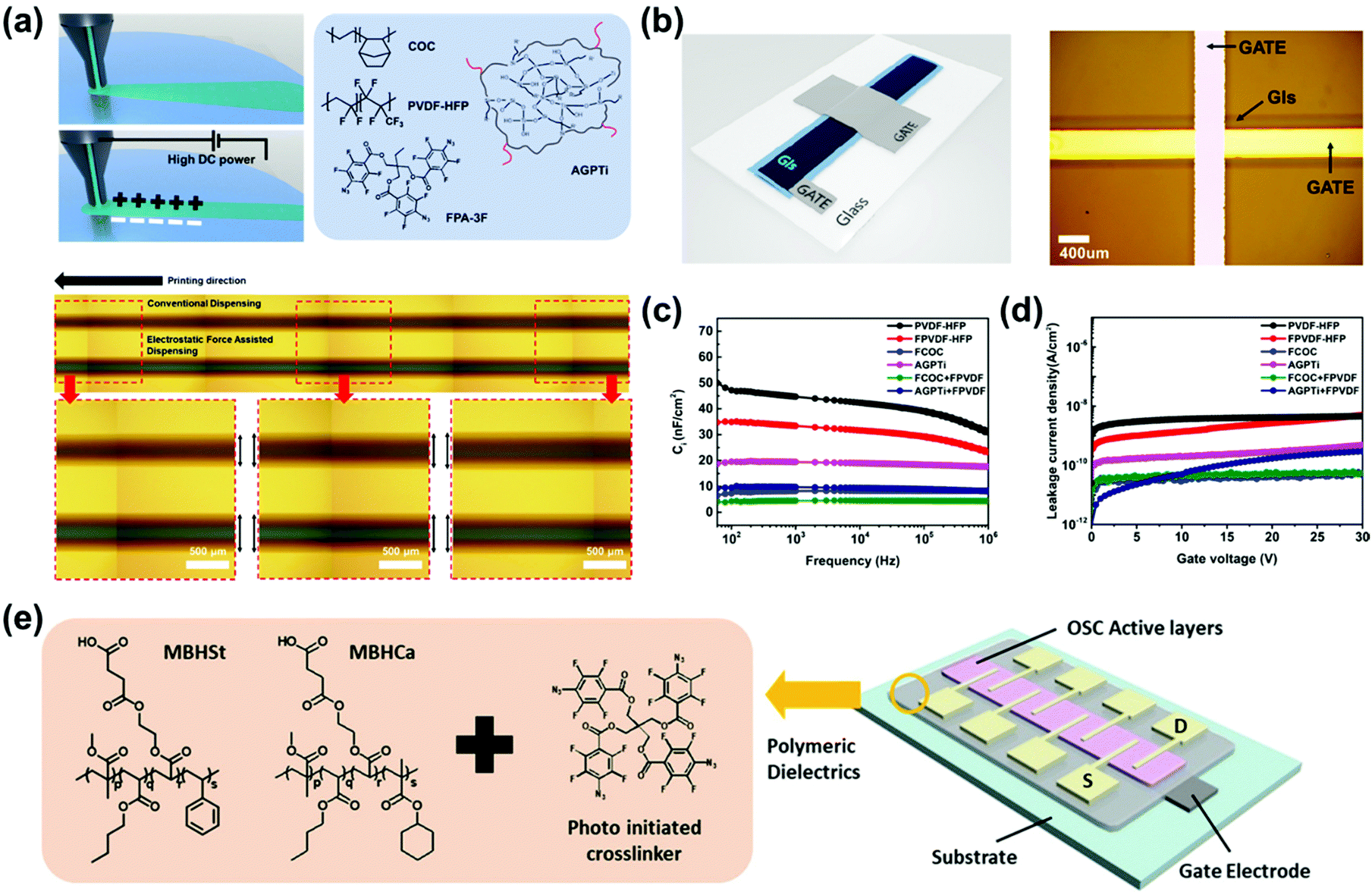 | ||
| Fig. 9 (a) Schematic illustration of the conventional dispensing and electrostatic-force-assisted dispensing, chemical structure of various insulators, and OM image of PVDF-HFP printed using conventional dispensing and electrostatic-force-assisted dispensing. (b) Schematic illustration and OM images, (c) areal capacitances, and (d) leakage current density values of the metal–insulator–metal capacitors with different EHD-printed insulator layers. (a–d) Reproduced from ref. 154 with permission from the American Chemical Society. (e) Schematic representation of the OTFT devices and chemical structure of novel acrylate polymer dielectrics (MBHSt and MBHCa) suitable for EHD printing. Reproduced from ref. 155 with permission from the Wiley-VCH. | ||
Low power consumption is an important requirement for OTFTs. Therefore, fabrication of flexible electronic products that operate at low voltage requires high-k organic insulating materials. Insulating polymeric materials containing carboxyl and hydrophobic functional groups can be blended to obtain high-k dielectric films that have a hydrophobic surface (Fig. 9e).155 The authors designed graft copolymers composed of different functional segments to obtain a hydrophobic surface and high-k properties. The solution processability of these materials enabled the production of nearly uniform films by EHD jet printing in the dragging mode. In this mode the droplet formed at the nozzle tip is in direct contact with the substrate under a steady electrostatic field. In addition, the thickness of the high-k dielectric films in this mode can be controlled easily by adjusting the solution concentration and the printing conditions. This ability facilitates the manufacture of reliable low-voltage OTFT devices.
Solid-state electrolyte insulators and ion gels have been printed using EHD jet printing.71 Ion-gel electrolytes are usually directly patterned using inkjet and aerosol jet printing methods; but use of the conventional EHD jet printing to print ion gels is a difficult task because the high number of ions in the ink hinder the formation of a Taylor cone in the cone-jet mode. Therefore, instead of the cone-jet mode, the authors used a dripping mode by using the electrostatic-force-assisted dispensing technique to produce an ion-gel pattern under the application of a very low voltage (Fig. 10a). This method forms a liquid bridge of ink between the nozzle and the substrate, and the bridge supplies a path for the ink under a very low electrostatic field and prevents unexpected jetting. This technique was used to prepare ion-gel patterns, which were then used in organic transistors that had EHD-printed PEDOT:PSS gate electrodes, P3HT semiconductors, and ion-gel dielectric layers (Fig. 10b). The resulting devices had good electrical characteristics and could operate at low voltage.
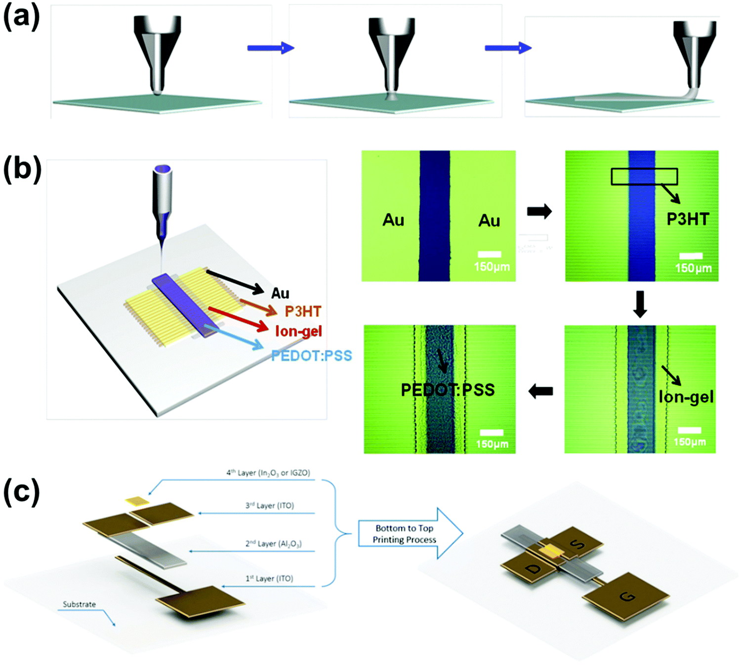 | ||
| Fig. 10 Schematic illustration for (a) ion-gel printing in a dripping mode using electrostatic-force-assisted dispensing, (b) top-gate, bottom contact transistor architecture, and optical microscope images for the sequential printing of P3HT, ion-gel and PEDOT:PSS onto the Au-prepatterned substrate. Reproduced from ref. 71 permission from the Elsevier. (c) Schematic diagrams of printing sequence of all-printed transistors using EHD-printed Al2O3 dielectric thin film. Reproduced from ref. 40 with permission from the American Chemical Society. | ||
The development of printing technology in the field of metal-oxide transistors has enabled fabrication of all-printed devices. Direct-printed metal-oxide transistors have been produced using high-k aluminum oxide (Al2O3) films obtained by EHD jet printing.40 Similar to the case of ion gels, homogeneous thin films are not easily produced by EHD jet printing of metal salt precursors, because the high ion concentration of the precursor solution causes inconsistency in the geometry of the ejected ink droplets. To solve this problem, a pulsed DC bias was applied such that the ions in the precursor close to the meniscus were redistributed, so the meniscus relaxed. The EHD-printed metal-oxide TFTs in their work consisted of a Al2O3 gate dielectric, ITO electrode contacts, and In2O3 and IGZO semiconductor channels, and had good electrical characteristics. EHD jet-printed Al2O3 can also be used as a passivation layer in metal-oxide transistors owing to the excellent moisture-barrier properties of Al2O3 thin films.156
3.4 Biomaterials
Jet printing of biomaterials requires high-resolution patterns of different materials, such as DNA, proteins, and hydrogels. Conventional inkjet printing has many biological applications, but when biomaterials are printed, the resolution is low, and this is a clear limitation. Resolution can be increased by increasing the number of dots per unit area. To achieve this purpose, EHD jet printing techniques can produce a thin jet of biomaterial.157EHD printing has been used to fabricate DNA probes that include nanoliter-scale droplets on the surfaces of inexpensive DNA microarrays.158 The size of the DNA droplets could be controlled from microliters to nanoliters by simply adjusting the strength of the electrical field. EHD jet printing has been used to generate a wide variety of single- and double-stranded DNA patterns with complex geometries. The patterns were then used to fabricate a simple aptamer-based biosensor to detect the fluorescence of adenosine molecules (Fig. 11a).159
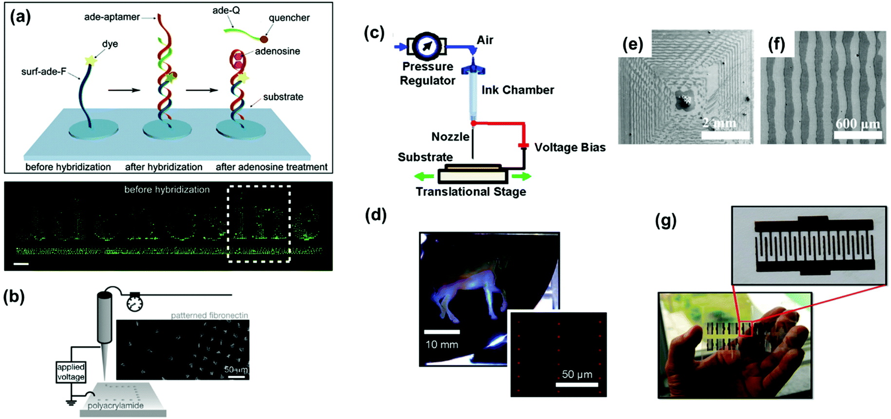 | ||
| Fig. 11 (a) Aptamer-based biosensor printed using EHD: schematic illustration for the detection of adenosine using aptamer patterns, and fluorescence micrograph of letters printed with [surf-ade-F] and underlined with [surf-no ade-F] as an internal control. Reproduced with ref. 159 with permission from the American Chemical Society. (b) Schematic illustration and SEM images for patterned fibronectin on polyacrylamide substrate. Reproduced from ref. 163 with permission of Wiley-VCH. (c) Schematic illustration for EHD equipment and (d) pictures of a large-area protein microarray, consisting of streptavidin–Cy5. Reproduced from ref. 168 with permission from the American Chemical Society. Ordered structures of EHD-printed poly(methylsilsesquioxane) maze topography with (e) low magnification and (f) high magnification. Reproduced from ref. 169 with permission from the Wiley-VCH. (g) Photograph of the fabricated bacteria sensors on a PET substrate, and their magnified image. Reproduced from ref. 172 with permission from the Springer Nature. | ||
EHD methods can also be used to deposit suspensions of living cells on surfaces without disrupting the cells’ structure or basic activities.160 Direct printing using EHD can fabricate 3D structures of collagen, which is a cell-adhesive biomaterial, and can draw patterns of viable bacteria.161,162 Fine jets of these biomaterials can be generated in the cone-jet mode when optimal additives such as ethylene glycol, phosphate buffer, and sodium chloride are used.162
EHD jet printing of biocompatible hydrogels can prepare scaffolds for cell delivery. The method has been used to produce an activated polyacrylamide hydrogel substrate that supported cell attachment and spreading by means of high-resolution patterns of cell adhesion proteins (Fig. 10b).163
Mixing living cells with appropriate hydrogels allows the corresponding bio-inks to be printed by EHD without affecting the survival of the cells. For example, alginate hydrogels that contained living cells were printed as three-dimensional constructs after optimizing the conditions of the EHD printing method.164 EHD-printed polyvinyl alcohol filaments and fluorescent microparticle patterns have been widely used in tissue-engineered scaffolds.165 Significant progress has been made to improve the feasibility of EHD printing for encapsulation of live cells.166,167
In general, use of EHD to print proteins is inefficient because the necessary high voltage can alter their secondary structure, and possibly diminish their biological functions and degrade the printing resolution. However, a high-speed pulsed printing technique can fabricate micro/nano patterns of several different proteins on various substrates (Fig. 11c and d).168 This work demonstrated the feasibility of using EHD to print diverse types of protein. Such printed protein microarrays have numerous potential applications in biology and medicine.
EHD can also print other biomaterials, such as polyurethane and poly(methylsilsesquioxane) polymers (Fig. 11e and f).169 Micron-sized polydiacetylene-embedded polystyrene nanofiber patterns have also been obtained.170 All of these biomaterials have important biomedical applications, such as in blood-contacting applications, tissue-engineered scaffolds, and skin-care products.
EHD can also fabricate biosensors. A flexible amperometric glucose sensor was fabricated using EHD to pattern glucose oxidase enzyme inks, which remained their glucose oxidase activity.171 EHD jet printing can produce all-printed electronic biosensors for rapid detection of a variety of pathogens (Fig. 11g), the biosensors can also be disposable.172 Flexible and disposable sensors developed using the EHD technique are expected to be ultimately used for point-of-care diagnostic platforms that connect to smart mobile devices.173
4. Conclusion
This paper has presented a comprehensive review of the basic principles of EHD jet printing and its electronic and biological applications, with an emphasis on materials that can be used as functional inks. EHD jet printing enables fabrication of micro- to nanoscale patterns of various materials, and thereby facilitates high-resolution, large-scale, and high-throughput manufacturing of electronic devices that have excellent properties. Several drawbacks of the EHD jet printing technique currently impede the commercialization of printed electronic products in a variety of industrial fields, but this printing technology is extremely attractive from multiple perspectives and is attracting a rapidly-growing interest. Therefore, we expect that the recent progress in various aspects of the EHD jet printing technology will advance the commercialization of printed electronic products in the near future.Conflicts of interest
There are no conflicts to declare.Acknowledgements
This work is financially supported by the National Research Foundation of Korea (NRF) grant funded by the Korea government (MSIT) (NRF-2020R1A2C1013018 and 2020R1A6A1A03038697). This research was also supported by Korea Basic Science Institute (National research Facilities and Equipment Center) grant funded by the Ministry of Education (2021R1A6C103A367).References
- Y. Khan, A. Thielens, S. Muin, J. Ting, C. Baumbauer and A. C. Arias, Adv. Mater., 2020, 32, 1905279 CrossRef CAS PubMed.
- S. K. Garlapati, M. Divya, B. Breitung, R. Kruk, H. Hahn and S. Dasgupta, Adv. Mater., 2018, 30, 1707600 CrossRef PubMed.
- L.-Y. Zhou, J. Fu and Y. He, Adv. Funct. Mater., 2020, 30, 2000187 CrossRef CAS.
- J. Smith, S. Chung, J. Jang, C. Biaou and V. Subramanian, IEEE Trans. Electron Devices, 2017, 64, 4310–4316 CAS.
- Y. Khan, F. J. Pavinatto, M. C. Lin, A. Liao, S. L. Swisher, K. Mann, V. Subramanian, M. M. Maharbiz and A. C. Arias, Adv. Funct. Mater., 2016, 26, 1004–1013 CrossRef CAS.
- M. G. Mohammed and R. Kramer, Adv. Mater., 2017, 29, 1604965 CrossRef PubMed.
- E. Kunnari, J. Valkama, M. Keskinen and P. Mansikkamäki, J. Cleaner Prod., 2009, 17, 791–799 CrossRef.
- R. Das and X. He, Flexible, Printed and Organic Electronics 2020-2030: Forecasts, Technologies, Markets, IDTechEx LTd, 2019.
- M. Dyson, R. Das and R. Collins, Materials for Printed/Flexible Electronics 2021-2031: Technologies Applications, Market Forecasts, 2020 Search PubMed.
- K.-S. Kwon, M. K. Rahman, T. H. Phung, S. Hoath, S. Jeong and J. S. Kim, Flexible Printed Electron., 2020, 5, 043003 CAS.
- J. Leppäniemi, O.-H. Huttunen, H. Majumdar and A. Alastalo, Adv. Mater., 2015, 27, 7168–7175 CrossRef PubMed.
- F. C. Krebs, J. Fyenbo and M. Jørgensen, J. Mater. Chem., 2010, 20, 8994–9001 RSC.
- N. J. Wilkinson, M. A. A. Smith, R. W. Kay and R. A. Harris, Int. J. Adv. Des. Manuf. Technol., 2019, 105, 4599–4619 CrossRef.
- C. M. Homenick, R. James, G. P. Lopinski, J. Dunford, J. Sun, H. Park, Y. Jung, G. Cho and P. R. L. Malenfant, ACS Appl. Mater. Interfaces, 2016, 8, 27900–27910 CrossRef CAS PubMed.
- J. Kim, D. Chae, W. H. Lee, J. Park, J. Shin, B.-C. Kwon and S. Ko, Org. Electron., 2018, 59, 84–91 CrossRef CAS.
- G. Zheng, J. Jiang, H. Chen, G. Kang, X. Wang, W. Li and L. Lin, Mater. Sci. Technol., 2020, 1–25 CAS.
- G. I. Taylor and M. D. Van Dyke, Proc. R. Soc. London, Ser. A, 1969, 313, 453–475 Search PubMed.
- K. Barton, S. Mishra, A. Alleyne, P. Ferreira and J. Rogers, Control Eng. Pract., 2011, 19, 1266–1273 CrossRef.
- J.-U. Park, M. Hardy, S. J. Kang, K. Barton, K. Adair, D. k. Mukhopadhyay, C. Y. Lee, M. S. Strano, A. G. Alleyne, J. G. Georgiadis, P. M. Ferreira and J. A. Rogers, Nat. Mater., 2007, 6, 782–789 CrossRef CAS PubMed.
- J.-U. Park, S. Lee, S. Unarunotai, Y. Sun, S. Dunham, T. Song, P. M. Ferreira, A. G. Alleyene, U. Paik and J. A. Rogers, Nano Lett., 2010, 10, 584–591 CrossRef CAS PubMed.
- Y. Lee, S.-Y. Min and T.-W. Lee, Macromol. Mater. Eng., 2017, 302, 1600507 CrossRef.
- D. W. Kim, S.-Y. Min, Y. Lee and U. Jeong, ACS Nano, 2020, 14, 907–918 CrossRef CAS PubMed.
- G. Williams, De Magnete Book, John Wiley and Sons, New York, 1893 Search PubMed.
- A. K. Figen, Electrospun Materials and Their Allied Applications, 2020, pp. 53–69 DOI:10.1002/9781119655039.ch2.
- L. Rayleigh, London, Edinburgh Dublin Philos. Mag. J. Sci., 1882, 14, 184–186 CrossRef.
- J. Zeleny, Phys. Rev., 1917, 10, 1–6 CrossRef.
- K. Ghosal, C. Agatemor, N. Tucker, E. Kny and S. Thomas, Electrospinning: From Basic Research to Commercialization, The Royal Society of Chemistry, 2018, pp. 1–23 10.1039/9781788012942-00001.
- M. Cloupeau and B. Prunet-Foch, J. Aerosol Sci., 1994, 25, 1021–1036 CrossRef CAS.
- J. Fenn, M. Mann, C. Meng, S. Wong and C. Whitehouse, Science, 1989, 246, 64–71 CrossRef CAS PubMed.
- A. M. Gañán-Calvo, Phys. Rev. Lett., 1997, 79, 217–220 CrossRef.
- I. D. Cherney and B. O. Ryalls, J. Exp. Child Psychol., 1999, 72, 305–328 CrossRef CAS PubMed.
- F. J. Higuera, J. Fluid Mech., 2004, 513, 239–246 CrossRef.
- V. N. Morozov and T. Y. Morozova, Anal. Chem., 1999, 71, 3110–3117 CrossRef CAS PubMed.
- O. Yogi, T. Kawakami, M. Yamauchi, J. Y. Ye and M. Ishikawa, Anal. Chem., 2001, 73, 1896–1902 CrossRef CAS PubMed.
- C. H. Chen, D. A. Saville and I. A. Aksay, Appl. Phys. Lett., 2006, 89, 124103 CrossRef.
- A. M. GaÑÁN-Calvo, J. Fluid Mech., 2004, 507, 203–212a CrossRef.
- S.-Y. Min, T.-S. Kim, B. J. Kim, H. Cho, Y.-Y. Noh, H. Yang, J. H. Cho and T.-W. Lee, Nat. Commun., 2013, 4, 1773 CrossRef PubMed.
- I. Liashenko, J. Rosell-Llompart and A. Cabot, Nat. Commun., 2020, 11, 753 CrossRef CAS PubMed.
- S. Hong, J. W. Na, I. S. Lee, H. T. Kim, B. H. Kang, J. Chung and H. J. Kim, ACS Appl. Mater. Interfaces, 2020, 12, 39705–39712 CrossRef CAS PubMed.
- Y. Liang, J. Yong, Y. Yu, A. Nirmalathas, K. Ganesan, R. Evans, B. Nasr and E. Skafidas, ACS Nano, 2019, 13, 13957–13964 CrossRef CAS PubMed.
- T. H. Cho, N. Farjam, C. R. Allemang, C. P. Pannier, E. Kazyak, C. Huber, M. Rose, O. Trejo, R. L. Peterson, K. Barton and N. P. Dasgupta, ACS Nano, 2020, 14, 17262–17272 CrossRef CAS PubMed.
- G. I. Taylor, Proc. R. Soc. London, Ser. A, 1964, 280, 383–397 Search PubMed.
- S. Su, J. Liang, Z. Wang, W. Xin, X. Li and D. Wang, Nanoscale, 2020, 12, 24450–24462 RSC.
- D. Wang, X. Zhao, Y. Lin, T. Ren, J. Liang, C. Liu and L. Wang, Front. Mech. Eng., 2017, 12, 477–489 CrossRef.
- R. T. Collins, M. T. Harris and O. A. Basaran, J. Fluid Mech., 2007, 588, 75–129 CrossRef.
- A. Lee, H. Jin, H.-W. Dang, K.-H. Choi and K. H. Ahn, Langmuir, 2013, 29, 13630–13639 CrossRef CAS PubMed.
- S. An, M. W. Lee, N. Y. Kim, C. Lee, S. S. Al-Deyab, S. C. James and S. S. Yoon, Appl. Phys. Lett., 2014, 105, 214102 CrossRef.
- X. Li, Y. J. Jeong, J. Jang, S. Lim and S. H. Kim, Phys. Chem. Chem. Phys., 2018, 20, 1210–1220 RSC.
- L. Guo, Y. Duan, Y. Huang and Z. Yin, Micromachines, 2018, 9, 522 CrossRef PubMed.
- J. Bae, J. Lee and S. Hyun Kim, J. Appl. Polym. Sci., 2017, 134, 45044 CrossRef.
- X. Li, K. Kim, H. Oh, H. C. Moon, S. Nam and S. H. Kim, Org. Electron., 2019, 69, 190–199 CrossRef CAS.
- H. Lee, B. Seong, J. Kim, Y. Jang and D. Byun, Small, 2014, 10, 3918–3922 CrossRef CAS PubMed.
- X. Li, H.-j. Kwon, X. Qi, H. K. Choi, S. Lim, T.-W. Kim and S. H. Kim, J. Ind. Eng. Chem., 2020, 85, 269–275 CrossRef CAS.
- Y. Pan and L. Zeng, Micromachines, 2019, 10, 94 CrossRef PubMed.
- C. Wei and J. Dong, J. Manuf. Sci. Eng., 2014, 136, 061010 CrossRef.
- X. Zhao, D. Wang, Y. Lin, Y. Sun, T. Ren, J. Liang and M. Madou, Microsyst. Technol., 2019, 25, 4651–4661 CrossRef CAS.
- X. Yang, R. Liu, L. Li, Z. Yin, K. Chen and D. F. Wang, J. Electr. Eng., 2020, 71, 413–418 Search PubMed.
- D. A. Saville, Annu. Rev. Fluid Mech., 1997, 29, 27–64 CrossRef.
- D. Gao, D. Yao, S. K. Leist, Y. Fei and J. Zhou, Int. J. Bioprint., 2018, 5, 166 Search PubMed.
- K. Zhao, D. Wang, K. Li, C. Jiang, Y. Wei, J. Qian, L. Feng, Z. Du, Z. Xu and J. Liang, J. Electrochem. Soc., 2020, 167, 107508 CrossRef CAS.
- I. Marginean, P. Nemes, L. Parvin and A. Vertes, Appl. Phys. Lett., 2006, 89, 064104 CrossRef.
- S. Mishra, K. L. Barton, A. G. Alleyne, P. M. Ferreira and J. A. Rogers, J. Micromech. Microeng., 2010, 20, 095026 CrossRef.
- B. H. Kim, M. S. Onses, J. B. Lim, S. Nam, N. Oh, H. Kim, K. J. Yu, J. W. Lee, J.-H. Kim, S.-K. Kang, C. H. Lee, J. Lee, J. H. Shin, N. H. Kim, C. Leal, M. Shim and J. A. Rogers, Nano Lett., 2015, 15, 969–973 CrossRef CAS PubMed.
- Q. Wang, G. Zhang, H. Zhang, Y. Duan, Z. Yin and Y. Huang, Adv. Funct. Mater., 2021, 2100857 CrossRef CAS.
- M. S. Onses, E. Sutanto, P. M. Ferreira, A. G. Alleyne and J. A. Rogers, Small, 2015, 11, 4237–4266 CrossRef CAS PubMed.
- S. Coppola, G. Nasti, V. Vespini, V. Marchesano and P. Ferraro, ACS Omega, 2018, 3, 17707–17716 CrossRef CAS.
- A. Jaworek, J. Mater. Sci., 2007, 42, 266–297 CrossRef CAS.
- A. F. M. Altelaar, J. van Minnen, C. R. Jiménez, R. M. A. Heeren and S. R. Piersma, Anal. Chem., 2005, 77, 735–741 CrossRef CAS PubMed.
- S.-E. Park, S. Kim, D.-Y. Lee, E. Kim and J. Hwang, J. Mater. Chem. A, 2013, 1, 14286–14293 RSC.
- X. Li, T. Y. Yun, K.-W. Kim, S. H. Kim and H. C. Moon, ACS Appl. Mater. Interfaces, 2020, 12, 4022–4030 CrossRef CAS PubMed.
- E. M. Jung, S. W. Lee and S. H. Kim, Org. Electron., 2018, 52, 123–129 CrossRef CAS.
- D.-Y. Shin, S.-S. Yoo, H.-e. Song, H. Tak and D. Byun, Sci. Rep., 2015, 5, 16704 CrossRef CAS PubMed.
- K.-W. Kim, H. Oh, J. H. Bae, H. Kim, H. C. Moon and S. H. Kim, ACS Appl. Mater. Interfaces, 2017, 9, 18994–19000 CrossRef CAS PubMed.
- T. T. T. Can, T. C. Nguyen and W.-S. Choi, Adv. Eng. Mater., 2020, 22, 1901384 CrossRef CAS.
- J. Leitner, D. Sedmidubský, M. Lojka and O. Jankovský, Materials, 2020, 13, 2878 CrossRef CAS PubMed.
- T. T. T. Can, T. C. Nguyen and W.-S. Choi, Sci. Rep., 2019, 9, 9180 CrossRef PubMed.
- Q. Lei, J. He, B. Zhang, J. Chang and D. Li, J. Mater. Chem. C, 2018, 6, 213–218 RSC.
- I. J. Fernandes, A. F. Aroche, A. Schuck, P. Lamberty, C. R. Peter, W. Hasenkamp and T. L. A. C. Rocha, Sci. Rep., 2020, 10, 8878 CrossRef CAS PubMed.
- P. Patil, S. Patil, P. Kate and A. A. Kulkarni, Nanoscale Adv., 2021, 3, 240–248 RSC.
- J. Zhang, B. Geng, S. Duan, C. Huang, Y. Xi, Q. Mu, H. Chen, X. Ren and W. Hu, J. Mater. Chem. C, 2020, 8, 15219–15223 RSC.
- Z. Cui, Y. Han, Q. Huang, J. Dong and Y. Zhu, Nanoscale, 2018, 10, 6806–6811 RSC.
- Y. Han and J. Dong, Adv. Mater. Technol., 2018, 3, 1700268 CrossRef.
- H. Kim, J. A. Lee, C. P. Ambulo, H. B. Lee, S. H. Kim, V. V. Naik, C. S. Haines, A. E. Aliev, R. Ovalle-Robles, R. H. Baughman and T. H. Ware, Adv. Funct. Mater., 2019, 29, 1905063 CrossRef CAS.
- K.-H. Lee, S.-S. Lee, D. B. Ahn, J. Lee, D. Byun and S.-Y. Lee, Sci. Adv., 2020, 6, eaaz1692 CrossRef PubMed.
- S. Ali, A. Hassan, G. Hassan, J. Bae and C. H. Lee, Carbon, 2016, 105, 23–32 CrossRef CAS.
- H. Tran, V. R. Feig, K. Liu, H.-C. Wu, R. Chen, J. Xu, K. Deisseroth and Z. Bao, ACS Cent. Sci., 2019, 5, 1884–1891 CrossRef CAS PubMed.
- J. Yee Low, Z. Merican Aljunid Merican and M. Falalu Hamza, Mater. Today: Proc., 2019, 16, 1909–1918 Search PubMed.
- C. Zhan, G. Yu, Y. Lu, L. Wang, E. Wujcik and S. Wei, J. Mater. Chem. C, 2017, 5, 1569–1585 RSC.
- L. V. Kayser and D. J. Lipomi, Adv. Mater., 2019, 31, 1806133 CrossRef PubMed.
- B. Lyu, S. Im, H. Jing, S. Lee, S. H. Kim, J. H. Kim and J. H. Cho, ACS Appl. Mater. Interfaces, 2020, 12, 17799–17805 CrossRef CAS PubMed.
- S. Park, S. W. Heo, W. Lee, D. Inoue, Z. Jiang, K. Yu, H. Jinno, D. Hashizume, M. Sekino, T. Yokota, K. Fukuda, K. Tajima and T. Someya, Nature, 2018, 561, 516–521 CrossRef CAS PubMed.
- X. Tang, H.-j. Kwon, J. Hong, H. Ye, R. Wang, D.-J. Yun, C. E. Park, Y. J. Jeong, H. S. Lee and S. H. Kim, ACS Appl. Mater. Interfaces, 2020, 12, 33999–34010 CrossRef CAS PubMed.
- X. Tang, H.-j. Kwon, H. Ye, J. Y. Kim, J. Lee, Y. J. Jeong and S. H. Kim, Phys. Chem. Chem. Phys., 2019, 21, 25690–25699 RSC.
- D.-Y. Shin, J.-Y. Seo, H. Tak and D. Byun, Sol. Energy Mater. Sol. Cells, 2015, 136, 148–156 CrossRef CAS.
- B. Zhang, J. Lee, M. Kim, N. Lee, H. Lee and D. Byun, Micromachines, 2019, 11, 13 CrossRef PubMed.
- X. Li, E. M. Jung, K. S. Kim, J. H. Oh, T. K. An, S. W. Lee and S. H. Kim, Electron. Mater. Lett., 2019, 15, 595–604 CrossRef CAS.
- S. Ali, A. Hassan, G. Hassan, J. Bae and C. H. Lee, Org. Electron., 2017, 51, 119–127 CrossRef CAS.
- F. I. Alzakia, W. Jonhson, J. Ding and S. C. Tan, ACS Appl. Mater. Interfaces, 2020, 12, 28840–28851 CrossRef CAS PubMed.
- Y. J. Jeong, X. Lee, J. Bae, J. Jang, S. W. Joo, S. Lim, S. H. Kim and C. E. Park, J. Mater. Chem. C, 2016, 4, 4912–4919 RSC.
- X. Li, M. Go, S. Lim, T. K. An, Y. J. Jeong and S. H. Kim, Org. Electron., 2019, 73, 279–285 CrossRef CAS.
- S. H. Park, J. Kim, C. E. Park, J. Lee, H. S. Lee, S. Lim and S. H. Kim, Org. Electron., 2016, 38, 48–54 CrossRef CAS.
- J. Chang, J. He, Q. Lei and D. Li, ACS Appl. Mater. Interfaces, 2018, 10, 19116–19122 CrossRef CAS PubMed.
- T. Kamiya and H. Hosono, NPG Asia Mater., 2010, 2, 15–22 CrossRef.
- E. Fortunato, P. Barquinha and R. Martins, Adv. Mater., 2012, 24, 2945–2986 CrossRef CAS PubMed.
- M. Lee, J. W. Jo, Y. J. Kim, S. Choi, S. M. Kwon, S. P. Jeon, A. Facchetti, Y. H. Kim and S. K. Park, Adv. Mater., 2018, 30, 1804120 CrossRef PubMed.
- B. Sun and H. Sirringhaus, Nano Lett., 2005, 5, 2408–2413 CrossRef CAS PubMed.
- B. N. Pal, P. Trottman, J. Sun and H. E. Katz, Adv. Funct. Mater., 2008, 18, 1832–1839 CrossRef CAS.
- C.-s. Li, Y.-n. Li, Y.-l. Wu, B.-S. Ong and R.-O. Loutfy, J. Mater. Chem., 2009, 19, 1626–1634 RSC.
- K. Nomura, H. Ohta, A. Takagi, T. Kamiya, M. Hirano and H. Hosono, Nature, 2004, 432, 488–492 CrossRef CAS PubMed.
- S. Jeong, Y. Jeong and J. Moon, J. Phys. Chem. C, 2008, 112, 11082–11085 CrossRef CAS.
- S. Jeong, Y.-G. Ha, J. Moon, A. Facchetti and T. J. Marks, Adv. Mater., 2010, 22, 1346–1350 CrossRef CAS PubMed.
- S. Lee, J. Kim, J. Choi, H. Park, J. Ha, Y. Kim, J. A. Rogers and U. Paik, Appl. Phys. Lett., 2012, 100, 102108 CrossRef.
- S. Jeong, J.-Y. Lee, S. S. Lee, Y.-H. Seo, S.-Y. Kim, J.-U. Park, B.-H. Ryu, W. Yang, J. Moon and Y. Choi, J. Mater. Chem. C, 2013, 1, 4236–4243 RSC.
- Y. G. Lee and W. S. Choi, ACS Appl. Mater. Interfaces, 2014, 6, 11167–11172 CrossRef CAS PubMed.
- Y.-J. Kwack and W.-S. Choi, IEEE Electron Device Lett., 2013, 34, 78–80 CAS.
- Y. J. Jeong, J. Bae, S. Nam, S. Lim, J. Jang, S. H. Kim and C. E. Park, Org. Electron., 2016, 39, 272–278 CrossRef CAS.
- B. Zhang, J. He, J. Li, L. Wang and D. Li, Nanotechnology, 2019, 30, 475301 CrossRef CAS PubMed.
- S. Y. Kim, K. Kim, Y. H. Hwang, J. Park, J. Jang, Y. Nam, Y. Kang, M. Kim, H. J. Park, Z. Lee, J. Choi, Y. Kim, S. Jeong, B. S. Bae and J. U. Park, Nanoscale, 2016, 8, 17113–17121 RSC.
- K. Kang, D. Yang, J. Park, S. Kim, I. Cho, H.-H. Yang, M. Cho, S. Mousavi, K. H. Choi and I. Park, Sens. Actuators, B, 2017, 250, 574–583 CrossRef CAS.
- H. T. Yi, M. M. Payne, J. E. Anthony and V. Podzorov, Nat. Commun., 2012, 3, 1259 CrossRef PubMed.
- C. Reese, M. Roberts, M.-m. Ling and Z. Bao, Mater. Today, 2004, 7, 20–27 CrossRef CAS.
- T. Minari, C. Lui, M. Kano and K. Tskukagoshi, Adv. Mater., 2012, 24, 299–306 CrossRef CAS PubMed.
- Y. J. Jeong, H. Lee, B. S. Lee, S. Park, H. T. Yudistira, C. L. Choong, J. J. Park, C. E. Park and D. Byun, ACS Appl. Mater. Interfaces, 2014, 6, 10736–10743 CrossRef CAS PubMed.
- Y. Li, P. Sonar, L. Murphy and W. Hong, Energy Environ. Sci., 2013, 6, 1684–1710 RSC.
- Z. Yi, S. Wang and Y. Liu, Adv. Mater., 2015, 27, 3589–3606 CrossRef CAS PubMed.
- Q. Liu, S. E. Bottle and P. Sonar, Adv. Mater., 2020, 32, e1903882 CrossRef PubMed.
- K. Kim, C. Kim, Y. Jo, X. Tang, J.-H. Lee, H.-j. Kwon, J. Lee, S. H. Kim and T. K. An, J. Ind. Eng. Chem., 2019, 78, 172–177 CrossRef CAS.
- H. J. Cheon, X. Li, Y. J. Jeong, M. J. Sung, Z. Li, I. Jeon, X. Tang, H. G. Girma, H. Kong, S.-K. Kwon, T. K. An, S. H. Kim and Y.-H. Kim, J. Mater. Chem. C, 2020, 8, 8410–8419 RSC.
- Y. Lin, Y. Li and X. Zhan, Chem. Soc. Rev., 2012, 41, 4245–4272 RSC.
- K.-H. Kim, H. Yu, H. Kang, D. J. Kang, C.-H. Cho, H.-H. Cho, J. H. Oh and B. J. Kim, J. Mater. Chem. A, 2013, 1, 14538–14547 RSC.
- Y. Yu, Q. Ma, H. Ling, W. Li, R. Ju, L. Bian, N. Shi, Y. Qian, M. Yi, L. Xie and W. Huang, Adv. Funct. Mater., 2019, 29, 1904602 CrossRef CAS.
- K. Kim, J. Bae, S. H. Noh, J. Jang, S. H. Kim and C. E. Park, J. Phys. Chem. Lett., 2017, 8, 5492–5500 CrossRef CAS PubMed.
- K. Kim, G. Kim, B. R. Lee, S. Ji, S. Y. Kim, B. W. An, M. H. Song and J. U. Park, Nanoscale, 2015, 7, 13410–13415 RSC.
- B. W. An, K. Kim, M. Kim, S. Y. Kim, S. H. Hur and J. U. Park, Small, 2015, 11, 2263–2268 CrossRef CAS PubMed.
- D. Lembke and A. Kis, ACS Nano, 2012, 6, 10070–10075 CrossRef CAS PubMed.
- H. S. Lee, S. W. Min, Y. G. Chang, M. K. Park, T. Nam, H. Kim, J. H. Kim, S. Ryu and S. Im, Nano Lett., 2012, 12, 3695–3700 CrossRef CAS PubMed.
- D. Lembke, S. Bertolazzi and A. Kis, Acc. Chem. Res., 2015, 48, 100–110 CrossRef CAS PubMed.
- S. Lim, B. Cho, J. Bae, A. R. Kim, K. H. Lee, S. H. Kim, M. G. Hahm and J. Nam, Nanotechnology, 2016, 27, 435501 CrossRef PubMed.
- F. I. Alzakia, W. Jonhson, J. Ding and S. C. Tan, ACS Appl. Mater. Interfaces, 2020, 12, 28840–28851 CrossRef CAS PubMed.
- T. T. T. Can, Y.-J. Kwack and W.-S. Choi, Mater. Des., 2021, 199, 109408 CrossRef CAS.
- T. T. T. Can, H. L. Ko and W. S. Choi, Nanotechnology, 2021, 32, 245710 CrossRef CAS PubMed.
- C. R. Kagan, E. Lifshitz, E. H. Sargent and D. V. Talapin, Science, 2016, 353, aac5523 CrossRef PubMed.
- E. Nannen, J. Frohleiks and S. Gellner, Adv. Funct. Mater., 2020, 30, 1907349 CrossRef CAS.
- E. Jang, Y. Kim, Y.-H. Won, H. Jang and S.-M. Choi, ACS Energy Lett., 2020, 5, 1316–1327 CrossRef CAS.
- S. J. Kress, P. Richner, S. V. Jayanti, P. Galliker, D. K. Kim, D. Poulikakos and D. J. Norris, Nano Lett., 2014, 14, 5827–5833 CrossRef CAS PubMed.
- H. Li, Y. Duan, Z. Shao, G. Zhang, H. Li, Y. Huang and Z. Yin, Adv. Mater. Technol., 2020, 5, 2000401 CrossRef CAS.
- T. C. Nguyen, T. T. T. Can and W. S. Choi, Sci. Rep., 2019, 9, 13885 CrossRef PubMed.
- T. C. Nguyen and W. S. Choi, Sci. Rep., 2020, 10, 11075 CrossRef CAS PubMed.
- M. J. Grotevent, C. U. Hail, S. Yakunin, D. N. Dirin, K. Thodkar, G. Borin Barin, P. Guyot-Sionnest, M. Calame, D. Poulikakos, M. V. Kovalenko and I. Shorubalko, Adv. Opt. Mater., 2019, 7, 1900019 CrossRef.
- J. Shamsi, A. S. Urban, M. Imran, L. De Trizio and L. Manna, Chem. Rev., 2019, 119, 3296–3348 CrossRef CAS PubMed.
- M. D. Smith, B. A. Connor and H. I. Karunadasa, Chem. Rev., 2019, 119, 3104–3139 CrossRef CAS PubMed.
- H. C. Wang, Z. Bao, H. Y. Tsai, A. C. Tang and R. S. Liu, Small, 2018, 14, 1702433 CrossRef PubMed.
- Y. Altintas, I. Torun, A. F. Yazici, E. Beskazak, T. Erdem, M. Serdar Onses and E. Mutlugun, Chem. Eng. J., 2020, 380, 122493 CrossRef CAS.
- X. Tang, H. J. Kwon, Z. Li, R. Wang, S. J. Kim, C. E. Park, Y. J. Jeong and S. H. Kim, ACS Appl. Mater. Interfaces, 2021, 13, 1043–1056 CrossRef CAS PubMed.
- H. j. Kwon, H. Ye, K. Shim, H. G. Girma, X. Tang, B. Lim, Y. Kim, J. Lee, C. E. Park, S. H. Jung, J. M. Park, Y. J. Jung, D. H. Hwang, H. Kong and S. H. Kim, Adv. Funct. Mater., 2020, 31, 2007304 CrossRef.
- S. Hong, J. W. Na, I. S. Lee, H. T. Kim, B. H. Kang, J. Chung and H. J. Kim, ACS Appl. Mater. Interfaces, 2020, 12, 39705–39712 CrossRef CAS PubMed.
- Y. Han and J. Dong, J. Micro Nano-Manuf., 2018, 6, 040802 CrossRef.
- J. G. Lee, H. J. Cho, N. Huh, C. Ko, W. C. Lee, Y. H. Jang, B. S. Lee, I. S. Kang and J. W. Choi, Biosens. Bioelectron., 2006, 21, 2240–2247 CrossRef CAS PubMed.
- J.-U. Park, J. H. Lee, U. Paik, Y. Lu and J. A. Rogers, Nano Lett., 2008, 8, 4210–4216 CrossRef CAS PubMed.
- S. N. Jayasinghe, A. N. Qureshi and P. A. Eagles, Small, 2006, 2, 216–219 CrossRef CAS PubMed.
- H. S. Kim, D. Y. Lee, J. H. Park, J. H. Kim, J. H. Hwang and H. I. Jung, Exp. Tech., 2007, 31, 15–19 CrossRef.
- J.-H. Kim, D.-Y. Lee, J. Hwang and H.-I. Jung, Microfluid. Nanofluid., 2009, 7, 829–839 CrossRef CAS.
- M. J. Poellmann, K. L. Barton, S. Mishra and A. J. Johnson, Macromol. Biosci., 2011, 11, 1164–1168 CrossRef CAS PubMed.
- L. Gasperini, D. Maniglio, A. Motta and C. Migliaresi, Tissue Eng., Part C, 2015, 21, 123–132 CrossRef CAS PubMed.
- X. Zhao, J. He, F. Xu, Y. Liu and D. Li, Virtual Phys. Prototyping, 2016, 11, 57–63 CrossRef.
- L. Gasperini, D. Maniglio and C. Migliaresi, J. Bioact. Compat. Polym., 2013, 28, 413–425 CrossRef CAS.
- V. Liaudanskaya, L. Gasperini, D. Maniglio, A. Motta and C. Migliaresi, Tissue Eng., Part C, 2015, 21, 631–638 CrossRef CAS PubMed.
- K. Shigeta, Y. He, E. Sutanto, S. Kang, A. P. Le, R. G. Nuzzo, A. G. Alleyne, P. M. Ferreira, Y. Lu and J. A. Rogers, Anal. Chem., 2012, 84, 10012–10018 CrossRef CAS PubMed.
- Z. Ahmad, M. Rasekh and M. Edirisinghe, Macromol. Mater. Eng., 2010, 295, 315–319 CrossRef CAS.
- C. Song, J. A. Rogers, J.-M. Kim and H. Ahn, Macromol. Res., 2014, 23, 118–123 CrossRef.
- X. Du, C. J. Durgan, D. J. Matthews, J. R. Motley, X. Tan, K. Pholsena, L. Árnadóttir, J. R. Castle, P. G. Jacobs, R. S. Cargill, W. K. Ward, J. F. Conley and G. S. Herman, ECS J. Solid State Sci. Technol., 2015, 4, P3069–P3074 CrossRef CAS PubMed.
- S. Ali, A. Hassan, G. Hassan, C. H. Eun, J. Bae, C. H. Lee and I. J. Kim, Sci. Rep., 2018, 8, 5920 CrossRef PubMed.
- A. T. Jafry, H. Lee, A. P. Tenggara, H. Lim, Y. Moon, S.-H. Kim, Y. Lee, S.-M. Kim, S. Park, D. Byun and J. Lee, Sens. Actuators, B, 2019, 282, 831–837 CrossRef CAS.
Footnote |
| † These authors contributed equally to this work. |
| This journal is © The Royal Society of Chemistry 2021 |