
 Open Access Article
 This Open Access Article is licensed under a Creative Commons Attribution-Non Commercial 3.0 Unported Licence
The discovery of conductive ionic bonds in NiO/Ni transparent counter electrodes for electrochromic smart windows with an ultra-long cycling life†
Qi
Zhao
a,
Jinkai
Wang
 a,
Yuanyuan
Cui
a,
Xinghui
Ai
a,
Zhang
Chen
a,
Chuanxiang
Cao
a,
Feng
Xu
*b and
Yanfeng
Gao
*a
a,
Yuanyuan
Cui
a,
Xinghui
Ai
a,
Zhang
Chen
a,
Chuanxiang
Cao
a,
Feng
Xu
*b and
Yanfeng
Gao
*a
aSchool of Materials Science and Engineering, Shanghai University, 99 Shangda Rd., Shanghai, 200444, China. E-mail: yfgao@shu.edu.cn
bBeijing Key Laboratory of Lignocellulosic Chemistry, Beijing Forestry University, Beijing 100083, China. E-mail: xfx315@bjfu.edu.cn
First published on 25th May 2021
Abstract
Developing a highly stable electrode has been a research focus for electrochromic smart windows (ECSWs) with an ultralong cycling life. This paper reports a NiO/Ni counter electrode and the discovery of conductive ionic bonds at the NiO/Ni interface. The formation of these conductive ionic bonds between NiO and Ni is verified by electron localization function (ELF) and Bader charge analyses. Furthermore, the density of states (DOS) results reveal the metallic character of these ionic bonds. Such conductive ionic bonds stabilize the NiO lattice in the process of ion intercalation/deintercalation and weaken the electrostatic interaction between Ni and O. The experimental results show that the NiO/Ni electrode shows high visible transparency in the bleached state (90.1%), a fast switching speed (4.5 s for coloring and 5 s for bleaching) and an ultralong cycling life (87.0% retention of the original optical contrast at 550 nm after 10![[thin space (1/6-em)]](https://www.rsc.org/images/entities/char_2009.gif) 000 cycles). Additionally, a 10 cm × 10 cm ECSW assembled with this NiO/Ni counter electrode and a WO3 electrode shows excellent EC performances such as large optical contrast (67.1%@550 nm, −2 V), very small transparency (lower than 1% in the wavelength range of 1600–800 nm), and a high coloration efficiency of 175.7 cm2 C−1. This work on an all-solution preparation of NiO/Ni counter electrodes represents an important step toward the development of cheap ECSWs.
000 cycles). Additionally, a 10 cm × 10 cm ECSW assembled with this NiO/Ni counter electrode and a WO3 electrode shows excellent EC performances such as large optical contrast (67.1%@550 nm, −2 V), very small transparency (lower than 1% in the wavelength range of 1600–800 nm), and a high coloration efficiency of 175.7 cm2 C−1. This work on an all-solution preparation of NiO/Ni counter electrodes represents an important step toward the development of cheap ECSWs.
1. Introduction
Smart windows that can control solar gain or loss play an important role in energy-saving buildings, considering that 30–40% of the world's primary energy is used mainly for heating, cooling, ventilation, and appliances of buildings.1,2 To date, several types of smart windows have been explored, including thermochromic,3 mechano-thermochromic,4 photochromic5 and electrochromic6 smart windows. The application of thermochromic and photochromic smart windows is in progress. However, their optical properties are strongly dependent on the environmental temperature or light intensity.7 Electrochromic smart windows (ECSWs) can autonomously and reversibly change their transparency based on redox reactions by responding to an external voltage, which has been increasingly studied for decades as ideal devices for solar control.8 It is calculated that using electrochromic smart windows can decrease lighting costs by 50% and lower peak electricity power demand by up to 16% for commercial buildings.2 Typical ECSWs generally have a multilayer structure consisting of a working electrode, a counter electrode, an electrolyte providing ions, and two transparent conducting layers serving as electrical leads.9 To date, most studies have been conducted on the development of working electrodes, and only limited work has been conducted on counter electrodes. Additionally, a high-quality film of an appropriately chosen counter electrode material is of significant importance in decreasing the operating voltages and optimizing the EC performance (optical contrast, response time, and switching stability).10Nickel oxide (NiO) is one of the most promising electrode materials because of its high specific capacitance (2584 F g−1) and optical responses.11 Porous NiO films are especially attractive due to their good cycling performance (83% retention after 3000 cycles12 and 1000 cycles13). However, the cycle number of these porous NiO films via electrodeposition,12 chemical-bath deposition,13,14 hydrothermal15 and sputtering16 hardly exceeds 3000 (see Table 1 for details). Therefore, doping or the formation of NiO composites has been further investigated. To date, metal-doped NiO (Li+,17 Ti4+,18 Co2+,19 and Cu2+20) has led to an increase in the hole concentration, thus enhancing conductivity.19 However, the doping of elements can easily cause distortion of the NiO lattice, resulting in a decrease in crystallinity and collapse of the intercalation framework. On the other hand, carbon-based materials,21,22 conducting polymers23 and metals24 are widely considered as additives to increase the conductivity in combination with NiO. Liang et al.25 fabricated MOF-derived NiO@C films by a two-step pyrolysis. Because of the high conductivity of carbon and the construction of a hierarchical porous structure, NiO@C exhibited ultrastable cycling performance (90.1% retention after 20000 cycles). Lu et al.24 employed Ni–NiO heterostructured nanosheets as the cathode. The as-prepared Ni–NiO//Zn battery showed ultralong cycling durability (96.6% capacity retention after 10000 cycles). However, the low transmittance in the bleached states (either less than 70% or completely opaque) in these studies impedes the exchange of visual information in windows or displays. Most importantly, the effect of the interface of NiO composites has not been investigated systematically.
| Materials | Film preparation method | Cycle number | Electrolyte | Ref. |
|---|---|---|---|---|
| Porous NiO | Electrodeposition | 3000 (retain 83%) | 0.1 M KOH | 12 |
| Porous NiO | Photosensitive sol–gel method | 3000 (retain 90%) | 0.5 M KOH | 23 |
| Porous NiO | Chemical-bath deposition | 1000 | 1 M LiClO4/PC | 13 |
| Porous NiO | Chemical-bath deposition | 3000 | 0.5 M LiClO4/PC | 14 |
| Porous NiO | Sputtering | 1000 | 1 M LiClO4/PC | 16 |
| NiO microflakes | Hydrothermal | 2000 | 1 M LiClO4/PC | 15 |
| NiOX | Sputtering | 1100 | 1 M LiClO4/PC | 52 |
| Cu-Doped NiO | Electrodeposition | 100 | 0.1 M KOH | 20 |
| Li–Ti co-doped NiO | Sol–gel method | 200 | 0.1 M LiClO4/PC | 18 |
| Li-Doped NiO | Ultrasonic spray pyrolysis | 100 | 0.5 M LiClO4/PC | 17 |
| Li–Ta co-doped NiO | Sputtering | 500 | 1 M LiClO4/PC | 53 |
| NiO-MWCNTs | Electrostatic spray deposition | 2850 | 0.1 M NaOH | 21 |
| NiO/reduced graphene oxide | Electrophoretic deposition and chemical-bath deposition | 2200 | 1 M KOH | 22 |
| NiO/PPy | Electrodeposition and chemical-bath deposition | 10000 |
1 M LiClO4/PC | 49 |
| NiO/TiO2 | Electrochemial deposition and sol–gel method | 8000 | 0.5 M KOH | 50 |
A consensus has been reached that the formation of composites with high conductivity materials can promote electron transport, but the mechanism by which the ions and interfaces are affected remains unclear. G. Granqvist26 proposed that the insertion of ions could cause a change (expansion or contraction or both) in the NiO lattice. Dong27 suggested that the irreversible trapping of inserted ions should be responsible for the cycling degradation of NiO films. It could be concluded that ion diffusion played an important role in cycling performance, rather than only electron transport. Therefore, it is important to investigate the structure to guide the cycling process from both theoretical and experimental perspectives.
Enlightened by the above consideration, we developed a spray-coating process to prepare a highly stable and transparent NiO/Ni counter electrode (see Fig. 1 for details). The spray-coating method, as a typical solution-processed approach, has many advantages, such as excellent controllability, low energy consumption, simple film-forming equipment, and uniformity of the prepared film.28 The process was started with the fabrication of a mixture of Ni(OH)2/Ni powder via coprecipitation and a solvothermal method. A NiO/Ni film was obtained after annealing at 300 °C. Electrochemical characterization showed that the NiO/Ni electrode has an ultralong cycling life (87.0% retention of the original optical contrast at 550 nm after 10000 cycles) and a high bleached-state transmittance of 90.1%. This ultralong cycling life can be assigned to the formation of ionic bonds between NiO and Ni, which is confirmed by the electron localization function (ELF) and Bader charge analyses. Moreover, the DOS of the NiO–Ni interface area shows a metallic character. This conductive ionic bond enhances the electrochemical kinetics for the EC performance in terms of electrons and ions. Additionally, a 10 cm × 10 cm ECSW based on the NiO/Ni electrode exhibits good electrochromic performances such as large optical contrast (67.1%, 550 nm, −2 V), low NIR transparency (lower than 1% in the wavelength range of 1600–800 nm), and a high coloration efficiency of 175.7 cm2 C). This work provides a new theoretical idea for composite electrode materials and demonstrates an important step toward the solution processing of ECSWs.
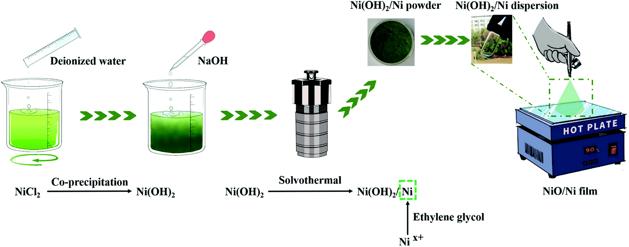 | ||
| Fig. 1 Schematic illustration of the preparation of the NiO/Ni electrode. | ||
2. Experimental procedures
2.1 Chemicals
Nickel chloride hexahydrate (NiCl2·6H2O, 98%), propylene carbonate (PC, 99%) and lithium perchlorate (LiClO4, 99.9%) were purchased from Aladdin. Ethylene glycol (EG) and isopropanol were purchased from Sinopharm Chemical Reagent Co., Ltd (China). Indium tin oxide (ITO)-coated glass (1.0 mm in thickness and 15 Ω in sheet resistance) was purchased from Zhuhai Kaivo Optoelectronic Technology Co., Ltd (China). Deionized (DI) water (>18 MΩ) was homemade. All reagents were used as received without further purification.2.2 Preparation of the Ni(OH)2/Ni nanopowder and dispersion
In a typical experiment, nickel chloride hexahydrate (100 g) was dissolved in deionized water (200 mL) with constant stirring. After dissolving completely, 10 M NaOH was added dropwise until reaching pH = 10, and a precipitate was obtained. The precipitate was washed sequentially with deionized water and ethanol to remove chlorine ions and other remnants by centrifugation. Then, the above precipitate was added to ethylene glycol, and a precursor of the nickel compounds was obtained. The green precursor solution was transferred into a 200 mL Teflon-lined autoclave. The hydrothermal reaction was carried out at 200 °C for 12 h. Finally, after washing and drying, a dark-green Ni(OH)2/Ni nanopowder product was obtained.The above Ni(OH)2/Ni nanopowder was added to isopropanol at a mass ratio of 1:19. After that, the mixture was milled with ZrO2 beads for 24 h at 3000 rpm. Thus, the Ni(OH)2/Ni dispersion was fabricated.
2.3 Preparation of the NiO/Ni counter electrode films
First, the Ni(OH)2/Ni dispersion was diluted using isopropanol at a 1:3 v/v ratio. Mixed dispersions (1 mL, 2 mL and 3 mL) were prepared. The ITO glass was placed on a hot plate at 90 °C to evaporate the solvent. Then, the mixed solution was sprayed onto ITO glass using a U-star air-brush. The distance between the nozzle and the ITO glass was maintained at 15 cm. The nozzle diameter was 0.3 mm, and the spraying pressure was 0.1 MPa. Finally, all the samples were heated at 5 °C min−1 and annealed at 300 °C for 1 h to establish good contact between the composite films and substrates. The prepared counter films with 1 mL, 2 mL and 3 mL of mixed dispersion are denoted as NiO/Ni-1, NiO/Ni-2 and NiO/Ni-3, respectively.
2.4 Assembly of the 10 cm × 10 cm electrochromic smart window device
The electrochromic layer of WO3 quantum dots was sprayed on ITO glass,29 and the as-prepared NiO/Ni films were used as counter electrodes. The EC smart windows were sealed using a 3M tape, leaving one small gap, and then the 0.2 M LiClO4/PC liquid electrolyte was injected into the gap using a syringe. Finally, the injection ports were sealed with UV curing glue.2.5 Characterization
The surface morphology of the NiO/Ni films was characterized using a scanning electron microscope (SEM, JEOL 7600F, Tokyo, Japan), and the crystal phase of the samples was determined by X-ray diffraction (XRD, 3 kW, D/MAX2500V +/PC; Nippon Rigaku Corporation, Japan) using a Cu K-alpha radiation source. X-ray photoelectron spectroscopy (XPS) was carried out on a Thermo Scientific K-Alpha instrument. The optical transmittance of the samples was measured using a UV/Vis/NIR spectrophotometer (UH4150; Hitachi, Japan). Transmission electron microscopy (TEM) was conducted using an FEI Tecnai G2 F20. The electron–spin resonance (ESR) measurement was conducted on a Bruker EMXplus EPR spectrometer.2.6 Electrochemical and electrochromic measurements
The electrochemical and electrochromic measurements were carried out in a quartz cell containing 0.2 M LiClO4 in PC with an electrochemical workstation (CHI760E, CHI Instruments, USA) using a three-electrode system. The fabricated NiO/Ni films on ITO glass (2.5 cm × 3 cm) were used as the working electrode, and a standard Ag/AgCl electrode and a platinum plate were used as the reference and counter electrodes, respectively. Electrochemical impedance spectroscopy (EIS) measurements were conducted with a Versa STAT 3F electrochemical workstation by applying a sinusoidal voltage amplitude of 5 mV in the frequency range of 0.1–106 Hz.2.7 Calculation details
Density functional theory (DFT) was employed to perform first-principles calculations.30,31 The total energies and forces were calculated using the projector augmented wave method in the Vienna Ab initio Simulation Package (VASP).32–34 The exchange–correlation (XC) energy of electrons was described with the general gradient approximation (GGA) using the Perdew–Burke–Ernzerhof (PBE) functional.35 Since the standard density functional theory (DFT) could not adequately describe the physical properties of NiO due to the strong on-site Coulomb repulsion (strong correlation) between the d electrons of the Ni atoms, the DFT + method with U = 8.0 eV and J = 0.95 eV was used to correctly describe the electronic properties of NiO, where U and J represent the on-site screened Coulomb energy and exchange interactions, respectively.36 Regarding the Ni atoms in the metallic layer, no consideration was given to the Coulomb (U) and exchange (J) parameters.The valence electron configurations for the elemental constituents are as follows: Ni-3d84s2 and O-2s22p4. The plane-wave cutoff was 400 eV in all calculations. Relaxation was terminated when the force on each atom was smaller than 0.01 eV Å−1. The energy convergence criterion of the electronic self-consistency was chosen as 10−6 eV. Antiferromagnetic and ferromagnetic structures were adopted for NiO and Ni, respectively. The NiO–Ni interface was constructed with the NiO(111)//Ni(111) orientation and then optimized. The interface was made of 4 metallic Ni layers and 4 layers of alternating Ni and O atomic planes along the [1 1 1] direction. The in-plane unit cell was chosen as a 2 × 2 and 15 Å vacuum above the interface. The k-points for NiO and NiO/Ni interfaces are 12 × 12 × 12 and 9 × 9 × 1, respectively. The Bader charge analysis was used to calculate the charge transfer between Ni and O,37 and an electron localization function (ELF) was used to identify the bond type of NiO and the NiO–Ni interfaces.38 Theoretically, an ELF value of 0.5 indicates that Pauli repulsion has the same value as that in a uniform electron gas of the same density, whereas an ELF value smaller (or larger) than 0.5 corresponds to a local Pauli repulsion larger (or smaller) than that in a uniform electron gas. In other words, ELF = 0.5 represents the electron-gas-like pair probability, while ELF = 0 and ELF = 1 represent perfect delocalization and localization, respectively. In general, metallic bonding is supposed to be delocalized, while covalent bonding is supposed to be localized.39
3. Results and discussion
3.1 Investigation of the effect of the NiO/Ni interface
The XRD patterns of all the as-prepared powders exhibit Bragg peaks (2θ) at 19.25, 33.06, 38.54, 52.10, 59.05, and 62.72, which are indexed to (001), (100), (101), (102), (110), and (111) planes of hexagonal Ni(OH)2 (JCPDS#14-0117, Fig. 2A), respectively. In a solvothermal process, the multivalent state of Ni is partly reduced to metal Ni by ethylene glycol, forming Ni(OH)2/Ni composite powders. The Bragg peaks at 44.50, 51.84, and 76.37 correspond to (111), (200), and (220) planes of cubic Ni (JCPDS#04-0850).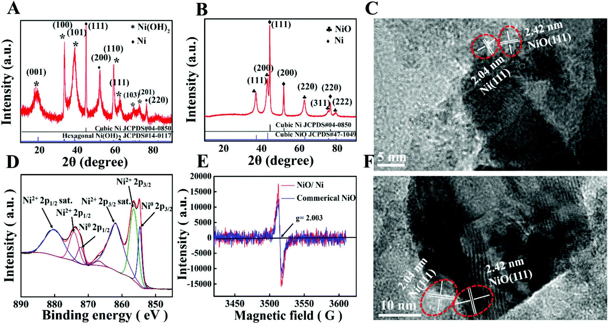 | ||
| Fig. 2 Phase characterization, electron–spin resonance spectroscopy and morphology of composite powders. (A) XRD pattern of the as-prepared Ni(OH)2/Ni powders. (B) XRD pattern of the as-prepared NiO/Ni powders. (C and F) TEM images showing the orientation of NiO(111)//Ni(111). (D) High-resolution XPS spectrum of the Ni 2p region for the NiO/Ni powders. (E) ESR spectra of NiO/Ni (red line) and commercial NiO (blue line). | ||
After thermal treatment, the dispersion (Ni(OH)2/Ni) is transformed into NiO/Ni (JCPDS#65-5745) (Fig. 2B). From the high-magnification TEM images (Fig. 2C and F), it is indicated that the (111) crystal faces of Ni are preferentially matched with the (111) crystal faces of NiO. The XPS result (Fig. 2D) manifests two groups of peaks at 874.2 and 856.5 eV, and 872.2 and 854.6 eV, which are assigned to Ni2+ 2p3/2 and Ni0, respectively.40 In addition, the presence of both metallic Ni0 and divalent Ni2+ as well as their satellite signals in the high-resolution XPS Ni 2p spectrum implies the coexistence of both metallic Ni and NiO, which is consistent with the XRD results.
To further investigate the chemical environments of the unpaired electrons in the NiO/Ni composite, electron-spin resonance (ESR) spectroscopy was performed. As demonstrated in Fig. 2E, the ESR spectra of NiO/Ni and commercial NiO exhibit a hyperfine structure with a symmetric signal located at approximately g = 2.003. Previous studies have suggested that the presence of a signal at g = 2.003 can be ascribed to the free electron signals.41 The order of the peak intensities is NiO < NiO/Ni, which implies that the composite powders do improve the concentrations of unpaired electrons.
To explore the reason for the increase in the free electrons of NiO/Ni and the effects of the interface between NiO and Ni, DFT calculations were conducted. After optimizing the interface distance of NiO–Ni in Fig. 3A, the interface structure is obtained. The average bond length of Ni and O at the interface is 2.070 Å, which is larger than the average bond length of Ni and O in NiO (2.028 Å), as shown in Fig. 3C. This difference can be explained by the electron localization function (ELF) and Bader charge analyses.
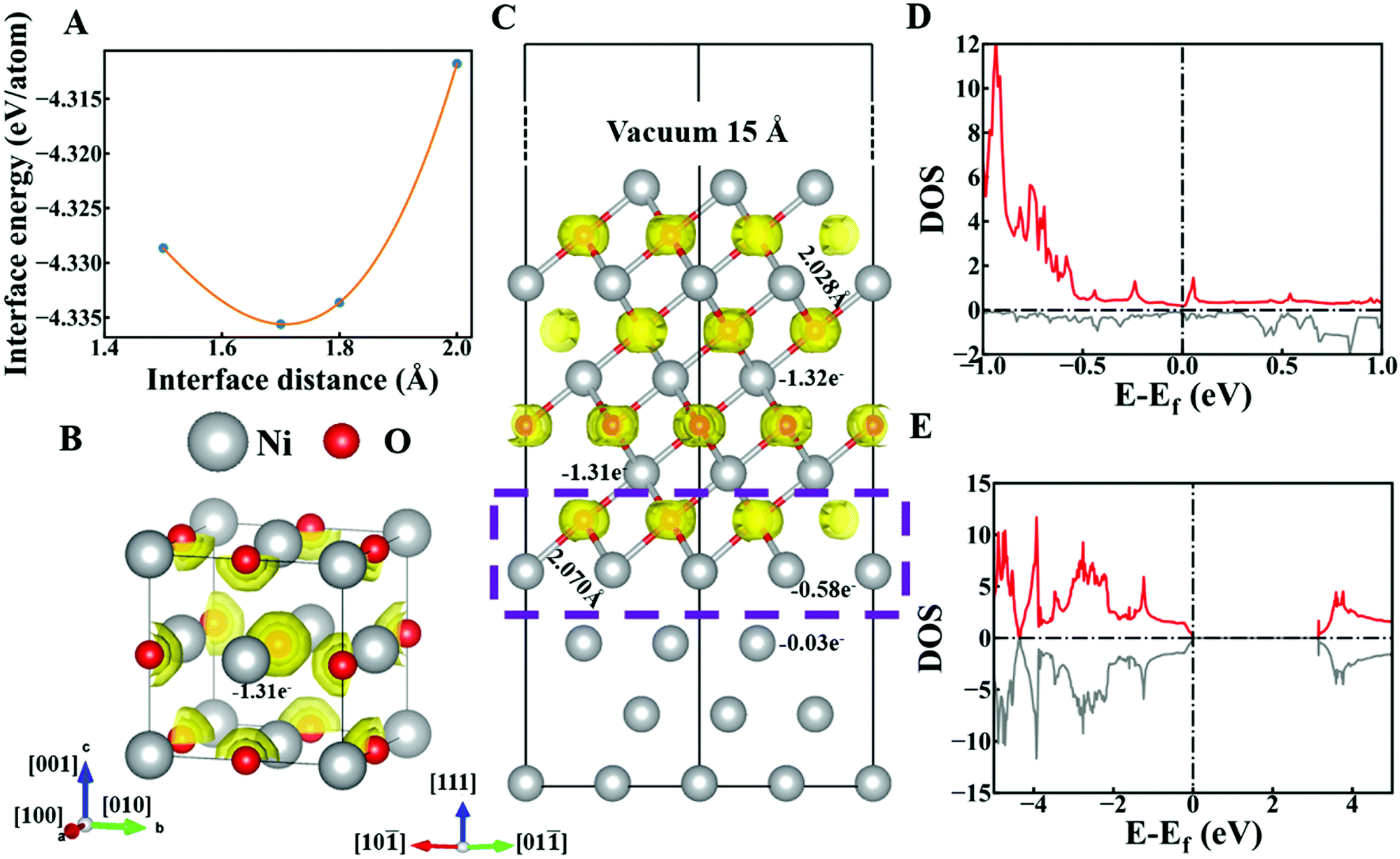 | ||
| Fig. 3 The nature of the NiO–Ni interface area from first principles simulation. (A) Interface energy with different interface distances. (B) ELF iso-surface (0.6) in bulk NiO and the corresponding charge transfer of Ni atoms. (C) NiO/Ni interface slab model with 15 Å vacuum and 0.6 ELF iso-surface value, and the corresponding charge transfer of Ni atoms. Atoms in the box with purple dotted-line form the interface area of NiO–Ni. (D) Density of states of the interface area in (C). (E) Density of states of the bulk NiO. | ||
Theoretically, an ELF value of 0.5 indicates that Pauli repulsion has the same value as that in a uniform electron gas of the same charge density, whereas an ELF value smaller (or larger) than 0.5 corresponds to a local Pauli repulsion larger (or smaller) than that in a uniform electron gas. In other words, ELF = 0.5 represents the electron-gas-like pair probability, while ELF = 0 and ELF = 1 represent perfect delocalization and localization, respectively. In general, metallic bonding is supposed to be delocalized, while covalent bonding is supposed to be localized.39 The iso-surface value of ELF is 0.6. As shown in Fig. 3B, electrons are localized around oxygen atoms, which suggests ionic bonding between the Ni and O in NiO. The Ni atom loses 1.31 electrons according to the Bader charge analysis. After forming an interface between Ni and NiO in Fig. 3C, the appearance of the ELF isosurface in the interface area (box with purple dotted line in Fig. 3C) indicates that the bonding mechanism in the interface area is the same as that in bulk NiO, which demonstrates the stability of the interface structure. However, the isosurfaces close to the interface area are slightly deformed compared with the isosurfaces in bulk NiO. The closer the isosurface is to the interface area, the more severe the deformation. The deformed isosurface indicates that the electrons are less localized than electrons in bulk NiO. The lower localization of electrons between Ni and O benefits the circulation of electrons. Moreover, the Ni atoms in the interface area lose only 0.58 electrons, which accounts for the lengthened Ni–O bond. The charge transfer of these 0.58 electrons also shows a weaker electrostatic interaction of Ni and O compared with that in bulk NiO, which promotes the electron transport.
The bonding mechanism and Bader charge analysis indicate that the NiO–Ni interface area serves as a stable “bridge” for ion and electron transfer between Ni and NiO. The density of states (DOS) of the interface provides more evidence. The DOS of NiO shows its semiconducting properties with a band gap of 3.46 eV as shown in Fig. 3E, while the DOS of the NiO–Ni interface area (Fig. 3D) shows a metallic character. Thus, a special conductive ionic bond at the interface is demonstrated.
3.2 Comparative analysis of the electrochemical and electrochromic properties of the NiO/Ni films
The morphology of the films can be observed in the SEM images of the NiO/Ni-1 films. From the low magnification SEM image (Fig. S1, ESI†), it can be observed that the surface morphological features of all of the films are smooth and uniform, and the high magnification images show that the films have a loose structure with many microholes, which are beneficial for improving the ion intercalation/extraction efficiency and EC behavior.12 Moreover, the thicknesses of films have certain effects on the optical properties and electrochemical behavior of a material.14 From the cross-sectional SEM image of the as-prepared samples (Fig. S2, ESI†), the thicknesses of the NiO/Ni-1, NiO/Ni-2 and NiO/Ni-3 films are 215 nm, 728 nm and 1169 nm, respectively.To further understand the charge transfer and Li+ mobility of the NiO/Ni films during the electrochemical process, electrochemical impedance spectroscopy (EIS) measurements were carried out in the frequency range of 0.1 Hz to106 Hz. It can be seen from Fig. 4A that the smaller semicircle in the EIS spectrum of NiO/Ni-1 implied easier electron transfer to the NiO lattice than that in thick films. In addition, the straight line is assigned to the Warburg impedance controlled by ion diffusion,42 which results in a steep slope and a high ion diffusion rate. Moreover, the Li+ diffusion coefficients of the NiO/Ni films with different thicknesses are calculated by the Randles–Sevcik equation from the voltammograms at different scan rates (Fig. 4B and C and Fig. S3 and S4 in the ESI†). The diffusion coefficients (D) of NiO/Ni-1, NiO-2, and NiO-3 are 1.93 × 10⁻⁹ cm2 s−1, 1.84 × 10⁻⁹ cm2 s−1 and 1.38 × 10⁻⁹ cm2 s−1, respectively, which are appropriately 1 order of magnitude larger than those of spherical NiO nanoparticles (1.22 × 10⁻¹⁰ cm2 s−1)43 and WO3 quantum dots (5.86 × 10⁻¹⁰ cm2 s−1).29 These results indicate that the conductive ionic bond promotes the rapid diffusion of Li+.
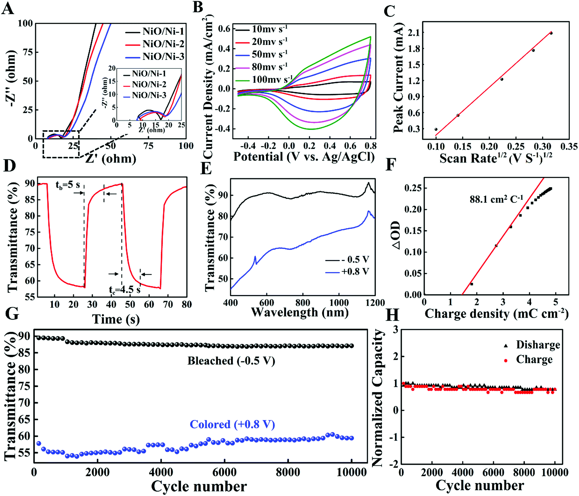 | ||
| Fig. 4 Optical and electrochemical measurements of the NiO/Ni films. (A) Nyquist plots of NiO/Ni-1, NiO/Ni-2 and NiO/Ni-3 films. The inset shows the magnified photographs of the semicircles. (B) Cyclic voltammograms of NiO/Ni-1 films at different scan rates (10 mV s−1, 20 mV s−1, 50 mV s−1, 80 mV s−1, and 100 mV s−1) in the voltage windows of −0.5 V to +0.8 V. (C) The ion diffusion coefficient calculated by the Randles-Sevcik equation. (D) Real-time transmittance spectrum at 550 nm in the −0.5/+0.8 V window (each for 20 s). (E) Transmittance spectra (400–1200 nm) in bleached (−0.5 V) and colored (+0.8 V) states. (F) Changes in the optical density (at 550 nm) with respect to the injected charge density (G) cycle performance between −0.5 V (10 s) and +0.8 V (10 s) to record in situ changes of transmittance at 550 nm. (H) Normalized charge and discharge capacity profiles of NiO/Ni-1 films in a 0.2 M LiClO4/PC electrolyte for 10000 cycles, −0.5 V (10 s) and +0.8 V (10 s) for one cycle. The value for the first cycle was set as 100%. | ||
The switching speed of electrochromic devices is essentially dependent on the ion diffusion coefficient and ion diffusion distance.44 As shown in Fig. 4D, the colouration (tc) and bleaching (tb) times of NiO/Ni-1, defined as the time required for 90% of the full optical modulation, are 4.5 s and 5 s, respectively, which are faster than those of previously reported NiO,11 WO3,45 TiO2−x46 films. Meanwhile, an increase in film thickness leads to a longer switching time (Fig. S5, ESI†). This phenomenon is probably related to the increase in diffusion depth (or diffusion length) with an increasing film thickness, which increases the difficulty of the charge/Li+ insertion/extraction process.14
The optical transmittance spectra of the NiO/Ni-1 films in the bleached and colored states from 1200 nm to 400 nm are shown in Fig. 4E. NiO/Ni-1 films show a 32.2% transmittance difference at 550 nm at applied potentials from −0.5 V to 0.8 V. More importantly, the transmittance of NiO/Ni-1 in the bleached state can reach 90.1%. When the range of voltages is increased (potentials from −0.8 V to 1 V), ΔT only increases by 1.8%, and the switching speed shows no obvious change (Fig. S6, ESI†). Another important performance indicator for electrochromic materials is the coloration efficiency (CE), defined as the optical density change per unit of charge injection (S7 in the ESI†). The calculated CE values of the NiO/Ni-1 films are the largest among those of the as-prepared samples (seen in Fig. 4F and Fig. S8, ESI†), reaching 88.1 cm2 C−1, which is also higher than those of previously reported NiO-based EC materials.19,22,47 The high CE performances are attributed to the intrinsic spectral response of the material and the thickness of the film. If the intrinsic CE of the material is high, the film requires less charge to switch and can be prepared with fewer raw materials.
High cycling stability is a significant criterion for evaluating the EC performance, which is a key part of practical applications. As presented in Fig. 4G and H, the NiO/Ni-1 film has an ultralong cycling life (after 10000 cycles, it still exhibits 87.0% retention in optical contrast and no obvious change in charge capacity), which is far higher than those of the reported NiO-based nanocomposite materials12–18,20–23,47–52 and other types of electrochromic materials (Table S1, ESI† and references therein). The excellent cycling stability in this work can be attributed to the following (Fig. 5A). (i) The formation of ionic bonds between NiO and Ni stabilizes their NiO/Ni interface, indicating that the intercalation and deintercalation of Li+ can hardly result in the collapse of the host structure of NiO. (ii) The interface area of NiO–Ni shows high conductivity, facilitating a more quick and efficient electron transport. (iii) The NiO/Ni film has a porous structure with a large surface area, such that the electrolyte can permeate effectively. For comparison, the cycling stability of the NiO/Ni-2 film exhibits a moderate decrease and maintains 66.1% after 6400 cycles, while the NiO/Ni-3 film only maintains 67.6% after 6400 cycles. (Fig. S9, ESI†). These results prove that the synthesized NiO/Ni films have excellent stability, but the thickness of the films has a certain effect on the stability because of the deeper channels in the film.14
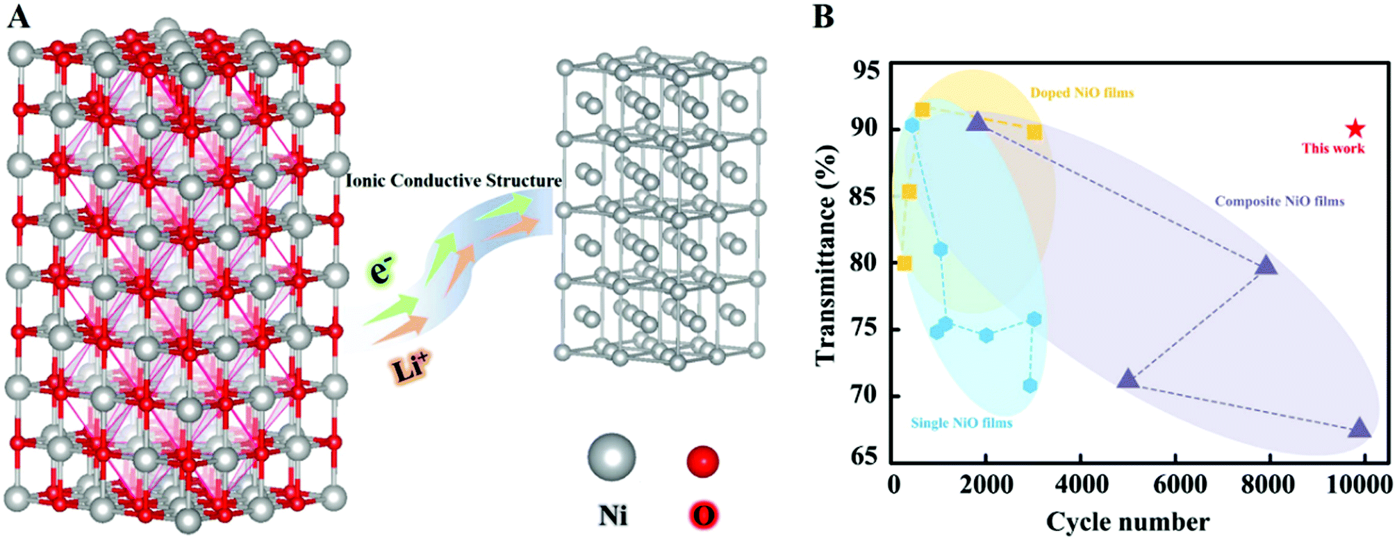 | ||
| Fig. 5 Schematic diagram and the summary of key electrochromic parameters. (A) Schematic of mechanism of ion +/e− transporting in NiO/Ni films. Conductive ionic bond allows electron transfer more efficiently and avoids ions to damage the structure of NiO in the process of extraction/insertion. (B) The summary of cycle numbers and the bleached-state transmittance of different NiO electrochoromic films: doped NiO films,18,48,52,53 composite NiO films and single NiO films,13,15,16,21–23,49,54–57 with the symbols of hexagon, square and triangle indicate the single NiO films, doped NiO films and composite NiO films, respectively. | ||
In summary, as seen in the EC parameters of the NiO/Ni samples in Table S2 (ESI†), we discover that the conductive ionic bond at the NiO/Ni interface makes the counter electrode attain excellent performance compared to any other electrochromic counterpart both in cycling life (10000 cycles) and transmittance in bleached states (90.1%)13,15,16,18,21–23,48,49,52–57 (Fig. 5B).
3.3 Analysis of the EC device performance
To verify the performance of the NiO/Ni counter electrode in electrochromic smart window devices, NiO/Ni and WO3 quantum dot films (homemade, our previous work)29 were utilized as anode and cathode electrodes to assemble an ECSW (Fig. 6A, size: 10 cm × 10 cm). Fig. 6D and E show that ΔT is 34.8%, 52.2%, and 67.1%, respectively, with voltages of −1 V, −1.5 V, and −2 V. Notably, when applied with −2 V, the ECSW possesses outstanding NIR-shielding properties: the transmittance is lower than 1% in the wavelength range from 1600 nm to 800 nm. In addition, as seen from Fig. 6B, it takes approximately 19 s and 22 s for coloring and bleaching, respectively. The CE of the device is 175.7 cm2 C−1 (Fig. 6C), which is much larger than that reported earlier.16,58 This result suggests that a small intercalation charge density can promote a large transmittance modulation. Remarkably, our ECSW also exhibits good cycling stability, reaching 79.3% of its initial optical contrast after 500 cycles (Fig. 6F), which is higher than that of a previously reported electrochromic device (size: 13.6 cm2, 57% retention after 200 cycles).59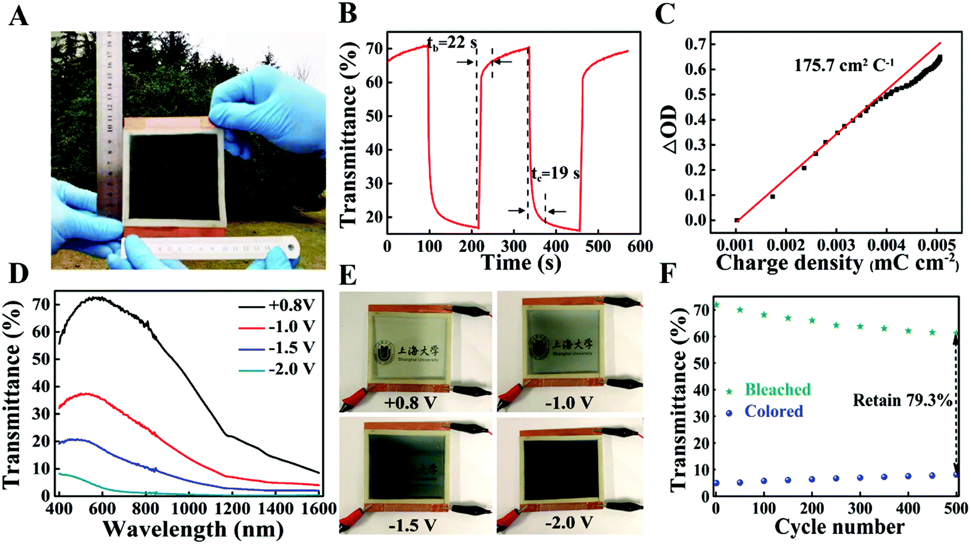 | ||
| Fig. 6 Digital photographs and electrochromic performance of a prototype device. (A) A digital photograph of 10 cm × 10 cm ECSWs. (B) A real-time transmittance spectrum at 550 nm in the −1.5 V/+0.8 V window (each for 120 s). (C) The relationship of optical density (at 550 nm) with respect to the injected charge density. (D) Transmittance spectra (400–1200 nm) in bleached (+0.8 V) and colored (−1 V, −1.5 V, −2 V) states and the (E) corresponding digital photographs. (F) Cycle performance with transmittance at 550 nm of the ESCW recorded between −2 V and +0.8 V. | ||
4. Conclusion
In conclusion, the investigation of the effect of the interface of NiO/Ni composites provides a deep understanding of the enhanced EC performance. The formation of a conductive ionic bond at the interface stabilizes the lattice of NiO and weakens the electrostatic interaction between Ni and O. In other words, the function of composites with highly conductive materials not only has a positive effect on electron transport but also facilitates ion diffusion in particular. The NiO/Ni electrode shows high transparency in its bleached states (90.1%), a fast switching speed (4.5 s for coloring and 5 s for bleaching) and an ultralong cycling life (after 10000 cycles, 87.0% retention of the original optical contrast at 550 nm). Moreover, a 10 cm × 10 cm ESCW exhibits excellent EC performance, including large optical contrast (67.1%, 550 nm, −2 V), outstanding NIR-shielding properties (lower than 1% in the wavelength range from 1600 nm to 800 nm), and a high coloration efficiency of 175.7 cm2 C−1. This all-solution process shows high potential for the mass production of inexpensive electrochromic windows.
Author contributions
Q. Z. and Y. F. G. conceived the idea of the study. Q. Z. performed the synthesis of the materials, the film deposition and electrochemical performance testing. J. K. W. and Y. Y. C. completed the first-principles simulation. X. H. A. prepared and characterized the electrochromic devices. Z. C. and X. C. C. analyzed the composition and morphology. Q. Z., Y. F. G. and F. X. wrote the paper, and all authors contributed to editing the manuscript.Conflicts of interest
The authors declare no competing interests.Acknowledgements
This work is supported by the Innovation Program of Shanghai Municipal Education Commission (No. 2019-01-07-00-09-E00020), the National Natural Science Foundation of China (51702209) and (51972206), Shanghai Municipal Science and Technology Commission (18JC1412800), the Open Project of State Key Laboratory of Advanced Special Steel, Shanghai Key Laboratory of Advanced Ferrometallurgy, Shanghai University (SKLASS 2019-04) and the Science and Technology Commission of Shanghai Municipality (No. 19DZ2270200).References
- H. N. Kim, D. Ge, E. Lee and S. Yang, Adv. Mater., 2018, 30, 1803847 Search PubMed.
- C. G. Granqvist, Sol. Energy Mater. Sol. Cells, 2012, 99, 1–13 Search PubMed.
- Y. Gao, H. Luo, Z. Zhang, L. Kang, Z. Chen, J. Du, M. Kanehira and C. Cao, Nano Energy, 2012, 1, 221–246 Search PubMed.
- Y. Ke, Q. Zhang, T. Wang, S. Wang, N. Li, G. Lin, X. Liu, Z. Dai, J. Yan, S. Magdassi, D. Zhao and Y. Long, Nano Energy, 2020, 73, 104785 Search PubMed.
- Y. Wang, E. L. Runnerstrom and D. J. Milliron, Annu. Rev. Chem. Biomol. Eng., 2016, 7, 283–304 Search PubMed.
- C. G. Granqvist, M. A. Arvizu, İ. B. Pehlivan, H.-Y. Qu, R.-T. Wen and G. A. Niklasson, Electrochim. Acta, 2018, 259, 1170–1182 Search PubMed.
- G. Cai, A. L. S. Eh, L. Ji and P. S. Lee, Adv. Sustainable Syst., 2017, 1, 1700074 Search PubMed.
- Q. Zhao, Y. Fang, K. Qiao, W. Wei, Y. Yao and Y. Gao, Sol. Energy Mater. Sol. Cells, 2019, 194, 95–102 Search PubMed.
- E. L. Runnerstrom, A. Llordés, S. D. Lounis and D. J. Milliron, Chem. Commun., 2014, 50, 10555–10572 Search PubMed.
- D. E. Shen, A. M. Österholm and J. R. Reynolds, J. Mater. Chem. C, 2015, 3, 9715–9725 Search PubMed.
- G. Cai, X. Wang, M. Cui, P. Darmawan, J. Wang, A. L.-S. Eh and P. S. Lee, Nano Energy, 2015, 12, 258–267 Search PubMed.
- Y. Yuan, X. Xia, J. Wu, Y. Chen, J. Yang and S. Guo, Electrochim. Acta, 2011, 56, 1208–1212 Search PubMed.
- H. Huang, J. Tian, W. Zhang, Y. Gan, X. Tao, X. Xia and J. Tu, Electrochim. Acta, 2011, 56, 4281–4286 Search PubMed.
- D. Dalavi, M. Suryavanshi, D. Patil, S. Mali, A. Moholkar, S. Kalagi, S. Vanalkar, S. Kang, J. Kim and P. Patil, Appl. Surf. Sci., 2011, 257, 2647–2656 Search PubMed.
- D. Ma, G. Shi, H. Wang, Q. Zhang and Y. Li, Nanoscale, 2013, 5, 4808–4815 Search PubMed.
- Z. Xie, Q. Liu, Q. Zhang, B. Lu, J. Zhai and X. Diao, Sol. Energy Mater. Sol. Cells, 2019, 200, 110017 Search PubMed.
- J. Denayer, G. Bister, P. Simonis, P. Colson, A. Maho, P. Aubry, B. Vertruyen, C. Henrist, V. Lardot and F. Cambier, Appl. Surf. Sci., 2014, 321, 61–69 Search PubMed.
- J. Zhou, G. Luo, Y. Wei, J. Zheng and C. Xu, Electrochim. Acta, 2015, 186, 182–191 Search PubMed.
- J.-h. Zhang, G.-f. Cai, D. Zhou, H. Tang, X.-l. Wang, C.-d. Gu and J.-p. Tu, J. Mater. Chem. C, 2014, 2, 7013–7021 Search PubMed.
- Y. Firat and A. Peksoz, Electrochim. Acta, 2019, 295, 645–654 Search PubMed.
- G.-f. Cai, J.-p. Tu, J. Zhang, Y.-j. Mai, Y. Lu, C.-d. Gu and X.-l. Wang, Nanoscale, 2012, 4, 5724–5730 Search PubMed.
- M. Garcia-Lobato, C. Garcia, A. Mtz-Enriquez, C. Lopez-Badillo, C. Garcias-Morales, E. Muzquiz-Ramos and B. Cruz-Ortiz, Mater. Res. Bull., 2019, 114, 95–100 Search PubMed.
- Y. Ren, X. Zhou, H. Zhang, L. Lei and G. Zhao, J. Mater. Chem. C, 2018, 6, 4952–4958 Search PubMed.
- Y. Zeng, Y. Meng, Z. Lai, X. Zhang, M. Yu, P. Fang, M. Wu, Y. Tong and X. Lu, Adv. Mater., 2017, 29, 1702698 Search PubMed.
- H. Liang, R. Li, C. Li, C. Hou, Y. Li, Q. Zhang and H. Wang, Mater. Horiz., 2019, 6, 571–579 Search PubMed.
- R.-T. Wen, G. A. Niklasson and C. G. Granqvist, Thin Solid Films, 2014, 565, 128–135 Search PubMed.
- D. Dong, W. Wang, A. Rougier, G. Dong, M. Da Rocha, L. Presmanes, K. Zrikem, G. Song, X. Diao and A. Barnabé, Nanoscale, 2018, 10, 16521–16530 Search PubMed.
- K. Li, Q. Zhang, H. Wang and Y. Li, J. Mater. Chem. C, 2016, 4, 5849–5857 Search PubMed.
- Y. Yao, Q. Zhao, W. Wei, Z. Chen, Y. Zhu, P. Zhang, Z. Zhang and Y. Gao, Nano Energy, 2020, 68, 104350 Search PubMed.
- P. Hohenberg and W. Kohn, Phys. Rev., 1964, 136, B864 Search PubMed.
- W. Kohn and L. J. Sham, Phys. Rev., 1965, 140, A1133 Search PubMed.
- G. Kresse and J. Furthmüller, Comput. Mater. Sci., 1996, 6, 15–50 Search PubMed.
- G. Kresse and D. Joubert, Phys. Rev. B: Condens. Matter Mater. Phys., 1999, 59, 1758 Search PubMed.
- P. E. Blöchl, Phys. Rev. B: Condens. Matter Mater. Phys., 1994, 50, 17953 Search PubMed.
- J. P. Perdew, K. Burke and M. Ernzerhof, Phys. Rev. Lett., 1996, 77, 3865 Search PubMed.
- K. Lee, É. D. Murray, L. Kong, B. I. Lundqvist and D. C. Langreth, Phys. Rev. B: Condens. Matter Mater. Phys., 2010, 82, 081101 Search PubMed.
- G. Henkelman, A. Arnaldsson and H. Jónsson, Comput. Mater. Sci., 2006, 36, 354–360 Search PubMed.
- C. F. Matta and R. J. Boyd, The quantum theory of atoms in molecules: From Solid State to DNA and Drug Design, Wiley-VCH Verlag GmbH & Co. KGaA, 2007 Search PubMed.
- A. Savin, R. Nesper, S. Wengert and T. F. Fässler, Angew. Chem., Int. Ed. Engl., 1997, 36, 1808–1832 Search PubMed.
- X. Ren, H. Lv, S. Yang, Y. Wang, J. Li, R. Wei, D. Xu and B. Liu, J. Phys. Chem. Lett., 2019, 10, 7374–7382 Search PubMed.
- F. Cui, L. Dou, Q. Yang, Y. Yu, Z. Niu, Y. Sun, H. Liu, A. Dehestani, K. Schierle-Arndt and P. Yang, J. Am. Chem. Soc., 2017, 139, 3027–3032 Search PubMed.
- J. A. Lee, M. K. Shin, S. H. Kim, H. U. Cho, G. M. Spinks, G. G. Wallace, M. D. Lima, X. Lepró, M. E. Kozlov and R. H. Baughman, Nat. Commun., 2013, 4, 1–8 Search PubMed.
- R. Goel, R. Jha and C. Ravikant, J. Phys. Chem. Solids, 2020, 144, 109488 Search PubMed.
- D. Qiu, H. Ji, X. Zhang, H. Zhang, H. Cao, G. Chen, T. Tian, Z. Chen, X. Guo and L. Liang, Inorg. Chem., 2019, 58, 2089–2098 Search PubMed.
- S. Zhang, S. Cao, T. Zhang, A. Fisher and J. Y. Lee, Energy Environ. Sci., 2018, 11, 2884–2892 Search PubMed.
- S. Zhang, S. Cao, T. Zhang and J. Y. Lee, Adv. Mater., 2020, 32, 2004686 Search PubMed.
- P. Saha, M. K. Datta, O. I. Velikokhatnyi, A. Manivannan, D. Alman and P. N. Kumta, Prog. Mater. Sci., 2014, 66, 1–86 Search PubMed.
- A. Sonavane, A. Inamdar, D. Dalavi, H. Deshmukh and P. Patil, Electrochim. Acta, 2010, 55, 2344–2351 Search PubMed.
- X. Qi, G. Su, G. Bo, L. Cao and W. Liu, Surf. Coat. Technol., 2015, 272, 79–85 Search PubMed.
- Z. Liu, Y. Huang, Y. Huang, Q. Yang, X. Li, Z. Huang and C. Zhi, Chem. Soc. Rev., 2020, 49, 180–232 Search PubMed.
- Y.-S. Lin, P.-W. Chen, D.-J. Lin, P.-Y. Chuang, T.-H. Tsai, Y.-C. Shiah and Y.-C. Yu, Surf. Coat. Technol., 2010, 205, S216–S221 Search PubMed.
- Q. Huang, Q. Zhang, Y. Xiao, Y. He and X. Diao, J. Alloys Compd., 2018, 747, 416–422 Search PubMed.
- D. Dong, W. Wang, G. Dong, F. Zhang, H. Yu, Y. He and X. Diao, RSC Adv., 2016, 6, 111148–111160 Search PubMed.
- S. Hou, X. Zhang, Y. Tian, J. Zhao, H. Geng, H. Qu, H. Zhang, K. Zhang, B. Wang and A. Gavrilyuk, Chem. – Asian J., 2017, 12, 2922–2928 Search PubMed.
- G. Cai, C. Gu, J. Zhang, P. Liu, X. Wang, Y. You and J. Tu, Electrochim. Acta, 2013, 87, 341–347 Search PubMed.
- E. O. Zayim, I. Turhan, F. Tepehan and N. Ozer, Sol. Energy Mater. Sol. Cells, 2008, 92, 164–169 Search PubMed.
- K. Purushothaman and G. Muralidharan, Mater. Sci. Semicond. Process., 2011, 14, 78–83 Search PubMed.
- G. Atak and Ö. D. Coşkun, Solid State Ionics, 2019, 341, 115045 Search PubMed.
- H. Li, C. J. Firby and A. Y. Elezzabi, Joule, 2019, 3, 2268–2278 Search PubMed.
Footnote |
| † Electronic supplementary information (ESI) available. See DOI: 10.1039/d1ma00384d |
| This journal is © The Royal Society of Chemistry 2021 |