
 Open Access Article
 This Open Access Article is licensed under a
 Creative Commons Attribution 3.0 Unported Licence
Two-dimensional or passivation treatment: the effect of hexylammonium post deposition treatment on 3D halide perovskite-based solar cells†
Stav
Rahmany
and
Lioz
Etgar
 *
*
The Hebrew University of Jerusalem, Institute of Chemistry, The Center for Nanoscience and Nanotechnology, Casali Center for Applied Chemistry, Jerusalem 91904, Israel. E-mail: lioz.etgar@mail.huji.ac.il
First published on 24th February 2021
Abstract
Much effort has been made to push the power conversion efficiency of perovskite solar cells (PSCs) towards the theoretical limit. Recent studies have shown that post deposition treatment of barrier molecules that might form 2-dimensional (2D) perovskite on top of already crystalized 3D perovskite can improve the device performance and enhance stability. Still, it is debatable whether a 2D perovskite can indeed be formed on top and if so, whether it significantly contributes to photovoltaic (PV) performance. In this work we focused on the effect of hexylammonium iodide (HAI), which functions as a barrier molecule, post deposition treatment on top of already crystalized Cs0.2FA0.8Pb(I0.8Br0.2)3 3D perovskite. The HAI treated devices showed mainly an increase in the open circuit voltage and in fill factor compare to the non-treated devices. Since a clear improvement in the PV parameters of the treated devices was observed, we wanted to determine whether HAI treatment results in a 2D perovskite layer or serves as a passivation layer on top of the 3D perovskite. In order to address this question, a series of optical and physical characterizations at the nanometric HAI/perovskite interface were performed. A high-resolution transmission electron microscopic image of the interface, including the Fourier transform, shows a different crystallographic structure. In addition, X-ray photoelectron spectroscopy (XPS), combined with an etching process using argon (Ar) gas, was used to determine the chemical composition of this nanometric interface. There was no evidence of a significant and continuous 2D structure due to the HAI treatment. Most of the HAI can be found on top of the perovskite surface, serving as a passivation layer; this reduces the recombination rate and enhances the photoluminescence quenching. Understanding how the interface of the perovskite/R-NH3 molecules can be treated is a key to enhance further the performance of these perovskite solar cells.
Introduction
Perovskite-based solar cells have become a key factor in the renewable energy field, and they are excellent candidates to replace existing technologies in the coming years. Hybrid perovskite is a semiconductor with an ABX3 structure in which A is a monovalent cation (MA+ = methylammonium, FA+ = formamidinium, Cs+ or Rb+), and B is a rare divalent metal (Pb+ or Sn+) that forms six coordinative bonds with a halide anion (X = I−, Br−, Cl−), creating a BX6 octahedral.1–3 It shows remarkable optical and electronic properties such as a direct and tunable bandgap, a high absorption coefficient, a long diffusion length, and small exciton binding energy. In addition, it is a solution-based fabrication process.4–8 In the last few years, perovskite-based solar cells have progressed impressively in terms of power conversion efficiency (PCE), exceeding 25%, approaching the theoretical limit.9 Currently, state-of-the-art perovskites can be composed of a mixture of several “A” site cations in addition to mixed halides.10–12 The mixed-cation mixed-halide perovskites are easier to prepare and have been shown to be more stable, and gain better efficiency, compared with the single-cation perovskites.13–16 The perovskite lattice dimensionality can be tuned by the size of the A site cation. According to the Goldschmidt tolerance factor, the radii of the perovskite components will dictate the symmetry of the crystal unit cell.17 The A site cation is limited in size to ∼2.6 Å; when a larger A cation (R-NH3) will form a separation between the BX6 sheets, acting as a barrier, a two-dimensional (2D) structure of (R-NH3)2BX4 will be formed.18–22 Recent studies have shown 3D/2D perovskite heterostructure formation by using a 2D molecular solution such as Hexylammonium iodide (HAI) as post deposition treatment on top of a crystalized 3D perovskite layer.To date, there has been an ongoing discussion regarding whether these alkyl ammonium molecules function as a passivation layer or form a 2D perovskite on top of the 3D perovskite. Gharibzadeh et al. reported faster hole extraction near the hole-selective contact after using benzylammonium bromide molecules as post treatment.23 Using the same molecule, Snaith et al. showed that it can suppress non-radiative charge recombination.24 In addition, it was shown that 2D post deposition treatment can provide moisture stability under high humidity conditions due to the hydrophobic nature of the barrier molecule.25 On the other hand, other studies showed that the 2D post deposition treatment enhanced the cell performance by forming a passivation layer on top of the 3D perovskite, improving the perovskite interface. Mahmud et al. demonstrated double-sided surface passivation by using n-butylammonium iodide, which reduced the non-radiative recombination.26 In other report butylammonium and hexylammonium were used as post treatment to these perovskite based cells which demonstrated enhancement of the photoluminescence lifetime and suppressed interfacial charge recombination. A correlation between the lengths of the organic cation and the surface passivation effect was found.27 In addition, Jiang et al. reported that phenethylammonium iodide post deposition treatment reduces the surface defects.28
Based on these studies, it can be concluded that this post deposition treatment is essential for promoting efficient and stable perovskite-based solar cells. Therefore, better understanding the interface of the perovskite and the R-NH3 treatment is a key to enhance further the performance of these perovskite solar cells.
In this research we investigated the perovskite surface following post deposition treatment with R-NH3 molecules in order to determine whether the R-NH3 post deposition treatment forms a 2D structure on top of the 3D perovskite or whether it acts as a passivation capping layer. To this end, we fabricated Cs0.2FA0.8Pb(I0.8Br0.2)3 3D perovskite-based solar cells; we treated them with Hexylammonium iodide (HAI) on top. We used several high-resolution characterization techniques such as the depth profile of XPS etching and focused ion beam (FIB), along with high-resolution transmission electron microscopy (HR-TEM), to obtain a high-resolution indication of this interface. In addition, X-ray diffraction (XRD), Photoluminescence (PL), potential decay, and charge extraction measurements were used to shed light on this interface, which is essential in order to further increase the perovskite solar cell efficiency.
Results and discussion
The 3D perovskite layer was deposited on top of a mesoporous TiO2 layer by using a mixed-cation mixed-halide perovskite composition of Cs0.2FA0.8Pb(I0.8Br0.2)3. Following thermal annealing and full crystallization of the perovskite layer, HAI solution was spin coated on top of it and annealed for 30 minutes (more details are found in the Experimental section). Next, hole transporting material (HTM) was deposited and gold back contact was thermally evaporated to complete the device. A schematic illustration of the process is presented in Fig. 1A. Immediately after the HAI deposition, we noticed a metallic greenish layer over the entire surface, as can be seen in Fig. S1 in the ESI.† The top view SEM (Fig. 1B) shows the surface of the non-treated sample in which the perovskite grains are fully exposed and notable. On the other hand, with the HAI-treated sample we observed a thin capping layer that covers the perovskite surface (Fig. 1C). In order to reveal the effect of the HAI treatment, first a cross section analysis was made by focused ion beam (FIB) of the treated and non-treated samples.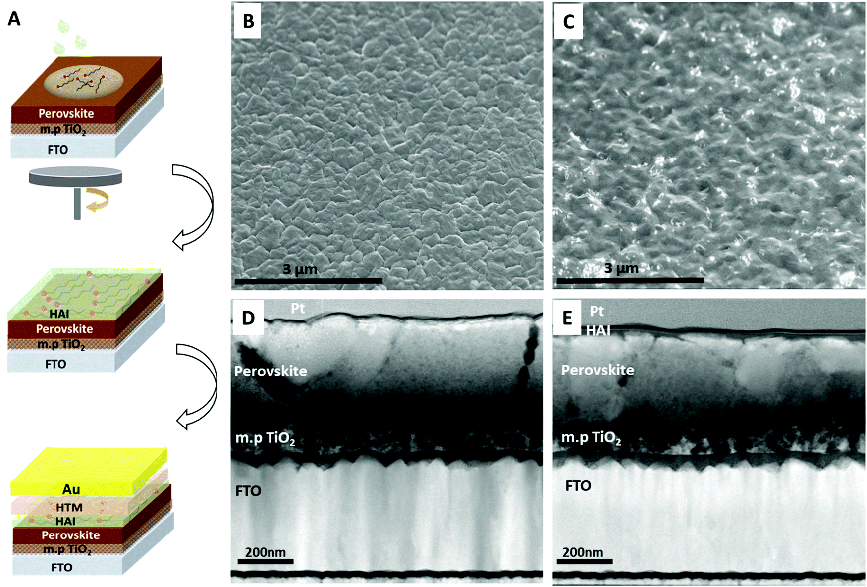 | ||
| Fig. 1 (A) Schematic illustration of the HAI post deposition on top of crystallized 3D perovskite and the complete structure of the solar cell. Scanning electron microscopy (SEM) images of the perovskite surface (B) without HAI treatment and (C) after HAI treatment. Focused ion beam (FIB) cross section images of (D) the non-treated and (E) the HAI-treated samples. All samples are without hole-transporting material. | ||
As a part of the FIB sample preparation, a protection layer of platina and carbon was deposited on top of the surface to prevent beam damage. Fig. 1D and E show cross sectional images of the non-treated and HAI-treated samples, respectively. It can be seen that when HAI is deposited on top of the perovskite, a thin over layer (∼15 nm) is present and uniformly covers the surface. We noted that during the SEM scanning the over layer on top of the perovskite surface had been damaged as a result of the electron beam (Fig. S2B, ESI†). After the removal of the HAI over layer, the perovskite grain boundaries can be clearly seen, as shown in Fig. S2C (ESI†).
To study the effect of the HAI layer on the photovoltaic parameters, we fabricated complete devices with and without HAI post deposition treatment. We noted that the wetting of the HTM solution, in the case of the treated devices, was poor, probably due to the hydrophobic nature that derives from the long carbon chain of the barrier molecules (HA in this case). We observed an increase in the power conversion efficiency (PCE) of more than 2.5% for the HAI-treated cells, compared with the standard devices, 15.0% ± 0.2 and 12.6% ± 0.2, respectively as presented in Fig. 2A. A closer examination revealed that this enhancement is due to an improvement in Voc (1.05 ± 0.01 V for treated, compared with 0.96 ± 0.01 V for non-treated) and fill factor (75.5% ± 0.5 compared to 71% ± 1), whereas the current density (Jsc) remains around the same value in both cases (19.1 ± 0.2 mA cm−2 and 18.6 mA cm−2 ± 0.4), as shown in Fig. 2B, C, and D, respectively.
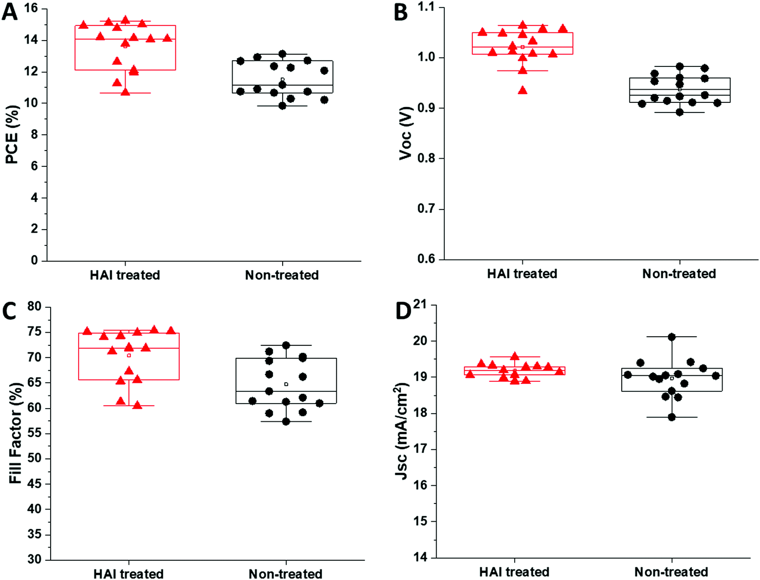 | ||
| Fig. 2 The (A) PCE, (B) Voc, (C) fill factor, and (D) current density of HAI-treated (red) and non-treated (black) devices. | ||
Moreover, we study the influence of different HAI concentrations (2, 5, and 10 mg ml−1) and IPA wash on the PV parameters (Table S1, ESI†). We noticed that there is no difference between the IPA washed devices to the 2 mg ml−1 and 5 mg ml−1 HAI treated devices in terms of the PV parameters. We found that the enhancement in the PV parameters become significant when using 10 mg ml−1 and 20 mg ml−1 HAI solution. The increase in the PCE for the high concentrations HAI-treated devices, compared with the low concentrations non-treated devices, was due to an enhancement in the Voc and the fill factor, whereas the current density remained the same, suggests that HAI forms a passivation layer, but not necessarily a two-dimensional (2D) perovskite layer on top of the already existing 3D perovskite, as was discussed previously in the literature.29 The HAI treatment compensates for the iodide vacancies that are present on the surface and at the grain boundaries, reducing the surface defects and enhancing the performance of the device. Moreover, the hydrophobic nature of the HAI molecules enhances the resistivity of the perovskite's surface to water therefore, it prevents degradation and serves as a protection layer. The hysteresis index (HI) for the treated and non-treated devices was calculated based on previous reports (Fig. S3 and Table S2, ESI†).30 We found that the HI for the HAI treated devices (0.070 ± 0.008) is one order of magnitude smaller in comparison with the non-treated devices (0.181 ± 0.034). The suppression of the hysteresis is further supporting the effect of HAI as a passivation treatment. To better understand the influence of the HAI post deposition treatment on the device's performance, charge extraction (CE) and potential decay (PD) measurements were performed, as shown in Fig. 3A and B, respectively. In both measurements the illumination intensity is 0.7 sun.
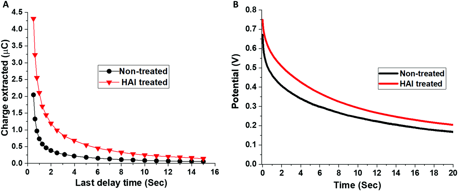 | ||
| Fig. 3 (A) Charge extraction and (B) voltage decay measurements for the non-treated (black) and the HAI-treated (red) devices. | ||
The CE measurements show that there are more charges at the starting point in the case of the HAI treated device compare to the non-treated although the illumination intensity and the experimental conditions are the same. In general, it can be seen that more charges are left to extract in the HAI-treated device for the whole range of delay times, compared with the non-treated device, where after a delay time of only 6 seconds, few charges are left to extract. The same trend can be noted from the PD measurements, where the potential decay is slower in the treated device during the entire measurement time. Both measurements indicate a slower recombination rate with the HAI-treated device. These findings support the assumption that HAI acts as a passivation layer that improves the holes’ injection into the HTM layer and that during this process recombination is prohibited.
Following the full device measurements, we focused on the perovskite/HAI/HTM interface. Photo-luminescence (PL) measurements were performed on samples of Perovskite/HTM, Perovskite/HAI/HTM, and Perovskite/HAI. Each sample was excited from both sides: the glass side and the film side (Fig. 4A), as shown in Fig. 4B–D, respectively. In the case of glass side excitation (blue curves), the beam directly hit the bottom part of the perovskite layer, which is probably not affected by the HAI post deposition treatment. On the other hand, excitation from the film side (green curves) will excite electrons that are close to the HAI-treated perovskite surface.
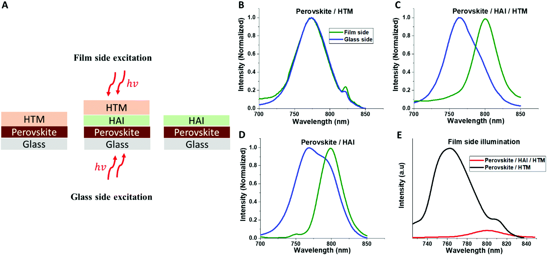 | ||
| Fig. 4 (A) Schematic illustration of the film and glass side PL excitation for different samples. PL measurements of (B) perovskite/HTM, (C) perovskite/HAI/HTM, and (D) perovskite/HAI, when the excitation is from the glass side (blue) and the film side (green). (E) PL intensity differences between HAI-treated (red) and non-treated (black) perovskite films including the HTM layer. | ||
Excitation from the film side will allow us to better understand the interfaces for HAI and perovskite. With the non-treated device (Perovskite/HTM), it can be seen that no difference exists in the PL peak position between both sides of the excitation. Accordingly, we can conclude that HTM does not affect the optical properties of the perovskite. However, with the HAI-treated samples (with and without HTM), we see the same trend, where the PL peak from the film side is ∼30 nm red-shifted, compared with the PL peak observed from the glass side. Assuming that a 2D formation exists on the perovskite surface due to a reaction of the HAI barrier molecule with the PbI2 residues, as discussed previously in literature,29 we would expect to obtain a blue shift in the position of the PL due to the wide band-gap of the 2D perovskite.
However, a red shift of the PL was observed. Our assumption is that halide exchange occurs in the Cs0.2FA0.8Pb(I0.8Br0.2)3/HAI interface where iodide from HAI exchanges some of the bromide from the 3D perovskite, which results in a red shift of the PL. This process has already been discussed in literature; halide exchange can occur in two ways: first, when the HAI solution drops on the perovskite surface, which forms a liquid–solid reaction.31 Second, during the HAI annealing stage, which creates a solid–solid reaction.32 Probably a contribution from both reactions occurs here. Next, we compared the PL intensity when the excitation is applied from the film side between HAI-treated (red) and non-treated (black) perovskites including the HTM layer in both cases. Fig. 4E shows that the intensity of the PL peak in the HAI-treated sample is significantly lower, compared with the non-treated perovskite PL peak. Since the excitation is from the film side, it can be concluded that HAI contributes to efficient hole injection or extraction from the perovskite to the HTM.
Hence, a thin lamella of the sample perovskite/HAI was cut by focused ion beam (FIB), which was further studied by high resolution transmission electron microscopy (HR-TEM). Fig. 5A shows a high magnification cross section of the perovskite/HAI structure, where the red squares denote the location where Fast Fourier transform (FFT) analysis was applied. We studied three different regions: the HAI layer (FFT1), the perovskite/HAI interface (FFT2), and deeper into the perovskite layer (FFT3). As can be seen, the FFT1 region does not exhibit any diffraction, meaning that probably no specific crystalline phase is formed in this region; this can be associated with the organic HAI passivation layer. FFT2 and FFT3 show clear diffraction patterns that indicate the existence of a crystalline material. d-Spacing calculations (Table S3, ESI†) show that those two regions share the same hkl planes of (0, 2, 1), which indicates a three-dimensional (3D) perovskite structure. Fig. 5B shows the perovskite/HAI interface at high magnification, which emphasizes the amorphous structure of the passivation layer, in contrast to the crystalline crystallographic planes that can be clearly seen in the perovskite region. In addition, it can be seen that the HAI capping layer has a thickness of ∼17 nm.
 | ||
| Fig. 5 High-resolution transition electron microscopy (HR-TEM) images of (A) HAI-treated perovskite and (B) the HAI perovskite interface. The red squares denote different regions in which the Fast Fourier transform (FFT) was applied; the inset shows the diffraction peak of each area. (C) X-ray photon spectroscopy (XPS) measurements, which show the elements’ concentration as a function of the Ar etching time, whereas the dashed line denotes the time in which the entire HAI layer was etched. (D) X-ray diffraction peaks of Cs0.2FA0.8Pb(I0.8Br0.2)3 (black), Cs0.2FA0.8Pb(I0.8Br0.2)3 after IPA wash (red), Cs0.2FA0.8Pb(I0.8Br0.2)3 after treated with 2 mg ml−1 (blue) and 20 mg ml−1 (green) HAI solution, two-dimensional (2D) HA2PbI4 (n = 1) (magenta), and HAI powder (orange). “*” indicates 3D perovskite peaks, “#” indicates 2D perovskite peaks. | ||
X-ray photoelectron spectroscopy (XPS), combined with an etching process using argon (Ar) gas, was used to determine the chemical composition of this nanometric interface. Using Ar gas, we can slightly etch the sample and simultaneously detect the chemical composition using XPS. Using this technique, we followed the atomic concentration of Carbon (black), Iodide (red), Nitrogen (blue), and lead (green) as a function of the etching time (depth), as presented in Fig. 5C. Each point represents the atomic concentration of the element after 10 seconds of Ar etching. Using this careful measurement, we can identify the components both at the surface and deeper into the film structure. The dashed line (etch time = 30 s) denotes the end of the HAI film (after ∼17 nm) and the interface with the 3D perovskite layer. It can be seen that the carbon and nitrogen concentration decrease, whereas the iodide and lead concentration increase as the Ar etching time increases, reaching saturation within the deviation range after 30 seconds. (It should be noted that the etching rate is not constant and depends on the specific elements which are being etched) At the beginning of the measurement, the carbon and nitrogen concentrations are relatively high, due to the presence of a carbon chain and amine groups of HAI, which cover the surface. As the etching becomes deeper inside the layer, the amount of carbon and nitrogen decreases and finally stabilizes at the interface of the perovskite/HAI. On the other hand, the iodide and lead concentration increases as the HAI film is being etched until it reaches the perovskite/HAI interface. The presence of both iodide and lead in the HAI film results from an unreacted excess of PbI2 on the perovskite surface, which mixes with the HAI film during the deposition. This is in addition to the iodide ions from the HAI molecule itself. To summarize, the XPS Ar etching provides additional proof of the presence of a passivation layer mainly composed of HAI molecules. To support our findings, we performed angle XPS measurements for the carbon and nitrogen atomic concentrations, as shown in Fig. S4A and B (ESI†), respectively. In this measurement the measured sample is tilted at a certain angle (up to 70 degrees), compared to the X-ray beam. Since the angle is smaller, the beam penetrates deeper into the surface. Unlike Ar etching XPS, this measurement does not harm the surface of the material and it penetrates less into the layer. We observed the same trend as previously mentioned, where in the HAI-treated sample the carbon concentration increases at high angles (close to the surface) as the nitrogen concentration decreases. For the non-treated sample we did not see an appreciable difference because the number of carbon and nitrogen atoms remains the same for all angles.
In order to see the structural changes in the 3D perovskite due to the HAI post deposition treatment, we compared the X-ray diffraction peaks of 3D perovskite, 3D perovskite with IPA wash, perovskite/HAI in a concentration of 2 mg ml−1 and 20 mg ml−1, 2D perovskite HA2PbI4 (n = 1), and HAI powder, shown in Fig. 5D. We chose the n = 1 2D perovskite, since it was previously reported that HAI can only react with PbI2 residues on the perovskite surface and no other “n” value can be formed due to the lack of an organic cation.33,34 The perovskite/IPA (red) and perovskite/HAI 2 mg ml−1 (blue) shows mainly 3D peaks in alignment with the non-treated perovskite (black). This indicates that most of the perovskite layer is composed of 3D perovskite. We notice a decrease in the intensity of the perovskite 001 peak at 14.1° and 220 peak at 28.5° while the PbI2 related peak at 12.7° become more dominant for both samples. We assume that the IPA dissolve the organic cation (FA+) within the perovskite lattice resulting to enhanced exposure of PbI2. It can be seen that the perovskite/HAI (2 mg ml−1) has similar diffraction peaks as the pure IPA sample without any indication of 2D perovskite related peaks. It can be concluded that at low concentration of HAI, there is no impact on the perovskite structure in terms of the formation of dimensionality. However, it can be seen that the 310 peak at 31.9° and 400 peak at 40.6° become more dominant in comparison to the non-treated perovskite film due to some structural changes as a result of the organic cation dissolution. In addition, the perovskite/HAI 20 mg ml−1 sample (green) shows similar peaks to the HAI powder sample (orange) at 4.0 and 5.5 degrees. A comparison between the perovskite/HAI sample and the 2D HA2PbI4 perovskite sample (magenta) shows two similar diffraction peaks at 10.8 and 21.8 degrees (denoted by “#”); these peaks correspond to n = 1. The intensity of these peaks is very low, which indicates that a small fraction of the perovskite has a 2D structure. It can be noticed that for the high HAI concentration sample the PbI2 peaks are suppressed which indicates that the formation of the 2D structure derives from the interaction between the HAI and the PbI2 that stays on the surface after the IPA dissolve some of the organic cation. We found that in the pure n = 1 sample the intensity of these peaks is 370 and 372 times larger than the same peaks in the perovskite/HAI sample.
In addition, we compared the intensities of the HA2PbI4 and 3D perovskite-related peaks in the perovskite/HAI sample (green). Importantly, we found that the dominant perovskite peak intensity at 14.1 degrees is ∼3 times higher compared with the HA2PbI4-related peaks at 10.8 and 21.8 degrees, shown in Table S4 and Fig. S5 (ESI†). In order to determine the amount of 2D perovskite that is formed after the HAI post treatment, we compared the intensity of the dominant HAI-related peak at 4.0 degrees to the intensities of the 2D-related peaks in the treated perovskite sample spectrum (Table S5, ESI†). We found that the HAI peak intensity is 12 and 10.5 times higher than the intensity of the 10.8 and 21.8 degrees peaks, respectively. These findings reveal that most of the HAI molecules remain in their original form, creating a capping over layer, and do not convert to 2D perovskite. Therefore, the HAI film functions as a passivation capping layer that prevents degradation, improves the interface with the HTM, and enhances the holes’ injection. In our opinion, even if two-dimensional perovskite is present in the passivation layer, it contributes very little.
Conclusions
In this work we focused on the formation of 2D perovskite on top of already existing Cs0.2FA0.8Pb(I0.8Br0.2)3 3D perovskite by using HAI as a barrier molecule. Similarly to previous reports, we found that HAI treatment enhances the PV performance mainly by increasing the Voc and fill factor of the device. In addition, charge extraction and potential decay measurements showed lower recombination rates with the HAI-treated device. Therefore, we focused on the interface of the perovskite/HAI. We found that HAI forms a thin and continuous layer on top of the perovskite, which serves mainly as a passivation layer. PL measurements showed a clear red shift of the perovskite/HAI interface along with enhanced quenching, compared with the non-treated perovskite. This indicates the formation of a passivation layer instead of the formation of 2D perovskite. In order to better understand the chemical and physical changes, we performed a unique XPS measurement, integrated with surface etching, which shows a clear change in the elements’ composition at the perovskite/HAI interface. FFT calculations showed a clear diffraction of 3D perovskite without any indication of the 2D structure, with HAI post treatment. Based on these findings, we can conclude that HAI post treatment forms a passivation layer on top of the 3D perovskite and that 2D perovskite formation is negligible. In our opinion it is possible to improve the PCE even more by modifying the HAI passivation layer thickness and adjusting it according to the HTM and perovskite thickness.Materials and methods
Substrate preparation
FTO (SnO2:F) coated glass (TEC 15, Pilkington) was etched by Zn and HCl (37% Aldrich) to form the electrode pattern. The patterned substrate were then sonicated with Hellmanex solution (2% in DI water) for 20 minutes follow by sonication in DI water, Acetone, and IPA for 10 minutes each. The clean substrates were then treated with O2 plasma for 15 minutes. Dense TiO2 layer was formed by spin coating a solution of 200 μl titanium diisopropoxidebis (TiDIP, 75% isopropanol, Aldrich) diluted in 1.5 ml Absolut Ethanol (>99%, Aldrich) at 5000 rpm for 30 seconds followed by 30 minutes annealing at 450 °C. ∼150 nm mesoporous TiO2 layer was formed by spin coating a diluted (1![[thin space (1/6-em)]](https://www.rsc.org/images/entities/char_2009.gif) :6 wt%) NR-30D paste (Great-Cell) with Absolute Ethanol at 5000 rpm for 30 seconds. The substrates were then dried at 100 °C for 10 minutes and gradually heated to 500 °C for 30 minutes. After cooling down the substrate were soaked in a TiCl4 bath contains 1.5 ml titanium chloride solution (5M, Wako) diluted with 150 ml TDW and kept in the oven for 30 minutes in 70 °C. The substrates were then washed with DI water and annealed at 450 °C for 30 minutes. After cooling down to 150 °C the substrates were immediately entered to N2 atmosphere glovebox for perovskite deposition.
:6 wt%) NR-30D paste (Great-Cell) with Absolute Ethanol at 5000 rpm for 30 seconds. The substrates were then dried at 100 °C for 10 minutes and gradually heated to 500 °C for 30 minutes. After cooling down the substrate were soaked in a TiCl4 bath contains 1.5 ml titanium chloride solution (5M, Wako) diluted with 150 ml TDW and kept in the oven for 30 minutes in 70 °C. The substrates were then washed with DI water and annealed at 450 °C for 30 minutes. After cooling down to 150 °C the substrates were immediately entered to N2 atmosphere glovebox for perovskite deposition.
Perovskite and HAI solutions preparation
A 1.2 M solution of Cs0.2FA0.8Pb(I0.8Br0.2)3 was made by dissolving stoichiometric amounts of CsI, PbI2 (10% excess), PbBr2 (Aldrich), and FAI (Great-Cell) in a mixture of anhydrous dimethyl formamide (DMF) and anhydrous dimethyl sulfoxide (DMSO) (Aldrich) with a ratio of 8.25:1.75, respectively. The solution was dissolve completely by vortex before heated to 60 °C. For the post deposition treatment we dissolved 20 mg of HAI powder in 1 ml of anhydrous isopropanol (>99%, Aldrich) and kept it on 60 °C overnight.
Device fabrication
After cooling down to room temperature 100 μl of perovskite solution was drop on each substrate and spin coated at two steps, 1000 rpm for 10 seconds followed by 5000 rpm for 35 seconds. 15 seconds before the end of the program 180 μl of chlorobenzene were quickly drop on top of the substrate forming light brown film. The perovskite film was then annealed at 100 °C for 40 minutes to achieve bright black perovskite film. The substrate cooled down for 10 minutes before the HAI deposition. To form the HAI layer 100 μl of HAI solution were dynamically spin coated on top of the perovskite layer at 4000 rpm for 30 seconds. The HAI coated perovskite films were then annealed at 120 °C for 20 minutes. The hole transport material (HTM) was made by dissolving 0.054 g of 2,2′,7,7′-tetrakis-(N,N-di-4-methoxyphenylamino)-9,9′-spirofluorine (spiro-OMeTAD) in 750 μl chlorobenzene. 13.1 μl of bis(trifluoromethane)sulfonimide lithium salt in acetonitrile (520 mg ml−1) and 21.6 μl of 4-tert-butylpyridine were add to the spiro solution after dissolving completely. The HTM solution was dynamically spin coated on top of the perovskite/HAI at 4000 rpm for 30 seconds. 70 nm of Au was thermally evaporated at a rate of 1.1 A s−1 under pressure of 5 × 10⁻⁶ torr to form the metallic back contact.XRD measurements
X-ray powder diffraction measurements were performed on the D8 Advance diffractometer (Bruker AXS, Karlsruhe, Germany) with secondary Graphite monochromator, 2° Sollers slits and 0.2 mm receiving slit. XRD patterns within the range 5° to 75° 2θ were recorded at room temperature using CuKα radiation (λ = 1.5418 Å) with following measurement conditions: tube voltage of 40 kV, tube current of 40 mA, step-scan mode with a step size of 0.02° 2θ and counting time of 1 s per step.Charge extraction and voltage decay
Both measurements were performed using Autolab Potentiostat–Galvanostat (PGSTAT) with a FRA32M LED driver equipped with a white light source when the illumination was from the back (glass) side. For voltage decay data collection and analysis we used Nova 2.1.1 software program. In the first step the cell was discharged for 2 seconds in the dark followed by 2 seconds of 0.7 Sun illumination. In the second step the light is shut off and the Voc is recorded in a period of 60 seconds. For the charge extraction measurements we used Nova 1.1 software program to collect and analyze the data. The first step is identical to the voltage decay measurements. In the next step the light is shut off and the system wait for certain time (delay time) before reconnecting and collecting the remained charges that didn’t recombine. The measurement have several cycles where in each cycle the delay time is extending between 0.5 to 15 seconds.Photovoltaic characterizations
The measurements of the photovoltaic parameters were made by using a New Port system, with an Oriel I-V test station and Oriel Sol3A simulator. Class AAA solar simulator was used for spectral performance, uniformity of irradiance and temporal stability. The device contains 450 W xenon lamp and the output power adjusted to match AM1.5 global sunlight (100 mW cm−2) as the spectral match classification were IEC60904-9 2007, JIC C 8912, and ASTM E927-05. I–V curves were extracted by applying an external bias to the cell and measuring the generated photocurrent with a Keithley model 2400 digital source meter. The pre-sweeping delay time was 10 seconds while the voltage stop was 10 mV and the delay time was 10 ms. The measurements were made by using a mask with an aperture area of 0.09 cm2.Photoluminescence (PL) measurements
The sample were prepared on top of 1.1 mm thickness glass slides. The perovskite solution was spin-coated at 2000 rpm and annealed at 100 °C for 30 minutes. The HAI and HTM deposition were made as described previously. For measuring the PL we used FluoroMax-4 spectrofluorometer (HORIBA). The samples were excited at 550 nm and the emission was recorded at 600–850 nm when the slit width was 5 nm.XPS measurements
The XPS spectra were measured using Kratos AXIS Supra spectrometer (Kratos Analytical Ltd, Manchester, U.K.) using an Al Kα monochromatic radiation X-ray source (1486.7 eV). Data were collected and analyzed by using ESCApe processing program (Kratos Analytical Ltd) and Casa XPS (Casa Software Ltd). The XPS spectra were acquired with a takeoff angle of 0° (normal to analyzer); vacuum condition in the chamber was 2 × 10⁻⁹ torr, the high-resolution XPS spectra were measured with pass energy of 20 and 0.1 eV step size. The binding energies were calibrated using C 1s peak energy as 285.0 eV.During the angle resolved XPS the measurements were taken in 0°, 30°, 45°, 60° and 70°. The XPS depth profiling was done using gas cluster ion source operated in Ar+ monoatomic mode, 5 kV, 20–30 cycles for 30 s (etching rate approximation is about 0.1 nm s−1).
Electron microscopy
High-resolution scanning transmission electron microscopy (STEM) imaging was done with probe corrected scanning transmission electron microscope themis-Z operated at 300 KV and equipped with SuperX EDS detector (Thermo Fisher Scientific, USA). STEM samples, cross section cuts, and top view images were prepared by using a focused ion beam scanning electron microscope (FIB, FEI Company, USA).Conflicts of interest
There are no conflicts to declare.Acknowledgements
We would like to thank the Israel Ministry of Energy and the Israel Science Foundation grant number: 2552/17 and 937/18.References
- D. B. Mitzi, Progress in Inorganic Chemistry, Wiley-Blackwell, 2007, vol. 48, pp. 1–121 Search PubMed.
- C. Li, X. Lu, W. Ding, L. Feng, Y. Gao and Z. Guo, Acta Crystallogr., Sect. B: Struct. Sci., 2008, 64, 702–707 CrossRef CAS.
- G. E. Eperon, S. D. Stranks, C. Menelaou, M. B. Johnston, L. M. Herz and H. J. Snaith, Energy Environ. Sci., 2014, 7, 982 RSC.
- S. A. Kulkarni, T. Baikie, P. P. Boix, N. Yantara, N. Mathews and S. Mhaisalkar, J. Mater. Chem. A, 2014, 2, 9221–9225 RSC.
- J. M. Ball, S. D. Stranks, M. T. Hörantner, S. Hüttner, W. Zhang, E. J. W. Crossland, I. Ramirez, M. Riede, M. B. Johnston, R. H. Friend and H. J. Snaith, Energy Environ. Sci., 2015, 8, 602–609 RSC.
- A. Walsh, J. Phys. Chem. C, 2015, 119, 5755–5760 CrossRef CAS.
- A. A. Zhumekenov, M. I. Saidaminov, M. A. Haque, E. Alarousu, S. P. Sarmah, B. Murali, I. Dursun, X. H. Miao, A. L. Abdelhady, T. Wu, O. F. Mohammed and O. M. Bakr, ACS Energy Lett., 2016, 1, 32–37 CrossRef CAS.
- S. D. Stranks, G. E. Eperon, G. Grancini, C. Menelaou, M. J. P. Alcocer, T. Leijtens, L. M. Herz, A. Petrozza and H. J. Snaith, Science, 2013, 342, 341–344 CrossRef CAS.
- Best Research-Cell Efficiency Chart|Photovoltaic Research|NREL, https://www.nrel.gov/pv/cell-efficiency.html, accessed 4 August 2020.
- N. Pellet, P. Gao, G. Gregori, T.-Y. Yang, M. K. Nazeeruddin, J. Maier and M. Grätzel, Angew. Chem., Int. Ed., 2014, 53, 3151–3157 CrossRef CAS.
- C. Yi, J. Luo, S. Meloni, A. Boziki, N. Ashari-Astani, C. Grätzel, S. M. Zakeeruddin, U. Röthlisberger and M. Grätzel, Energy Environ. Sci., 2016, 9, 656–662 RSC.
- M. Saliba, T. Matsui, J. Y. Seo, K. Domanski, J. P. Correa-Baena, M. K. Nazeeruddin, S. M. Zakeeruddin, W. Tress, A. Abate, A. Hagfeldt and M. Grätzel, Energy Environ. Sci., 2016, 9, 1989–1997 RSC.
- M. Grä, Acc. Chem. Res., 2017, 50, 487–491 CrossRef.
- J. W. Lee, D. H. Kim, H. S. Kim, S. W. Seo, S. M. Cho and N. G. Park, Adv. Energy Mater., 2015, 5, 1501310 CrossRef.
- L. K. Ono, E. J. Juarez-Perez and Y. Qi, ACS Appl. Mater. Interfaces, 2017, 9, 30197–30246 CrossRef CAS.
- W. Tan, A. R. Bowring, A. C. Meng, M. D. McGehee and P. C. McIntyre, ACS Appl. Mater. Interfaces, 2018, 10, 5485–5491 CrossRef CAS.
- V. M. Goldschmidt, Naturwissenschaften, 1926, 14, 477–485 CrossRef CAS.
- Z. Li, M. Yang, J. S. Park, S. H. Wei, J. J. Berry and K. Zhu, Chem. Mater., 2016, 28, 284–292 CrossRef CAS.
- B. Liu, C. M. M. Soe, C. C. Stoumpos, W. Nie, H. Tsai, K. Lim, A. D. Mohite, M. G. Kanatzidis, T. J. Marks and K. D. Singer, Sol. RRL, 2017, 1, 1700062 CrossRef.
- L. Zhang, Y. Liu, Z. Yang and S. (Frank) Liu, J. Energy Chem., 2019, 37, 97–110 CrossRef.
- C. Lan, Z. Zhou, R. Wei and J. C. Ho, Mater. Today Energy, 2019, 11, 61–82 CrossRef.
- J. Jagielski, S. Kumar, W. Y. Yu and C. J. Shih, J. Mater. Chem. C, 2017, 5, 5610–5627 RSC.
- S. Gharibzadeh, B. Abdollahi Nejand, M. Jakoby, T. Abzieher, D. Hauschild, S. Moghadamzadeh, J. A. Schwenzer, P. Brenner, R. Schmager, A. A. Haghighirad, L. Weinhardt, U. Lemmer, B. S. Richards, I. A. Howard and U. W. Paetzold, Adv. Energy Mater., 2019, 9, 1803699 CrossRef.
- Z. Wang, Q. Lin, F. P. Chmiel, N. Sakai, L. M. Herz and H. J. Snaith, Nat. Energy, 2017, 2, 17135 CrossRef CAS.
- C. Ma, C. Leng, Y. Ji, X. Wei, K. Sun, L. Tang, J. Yang, W. Luo, C. Li, Y. Deng, S. Feng, J. Shen, S. Lu, C. Du and H. Shi, Nanoscale, 2016, 8, 18309–18314 RSC.
- M. A. Mahmud, T. Duong, Y. Yin, H. T. Pham, D. Walter, J. Peng, Y. Wu, L. Li, H. Shen, N. Wu, N. Mozaffari, G. Andersson, K. R. Catchpole, K. J. Weber and T. P. White, Adv. Funct. Mater., 2020, 30, 1907962 CrossRef CAS.
- Y. Lv, X. Song, Y. Yin, Y. Feng, H. Ma, C. Hao, S. Jin and Y. Shi, ACS Appl. Mater. Interfaces, 2020, 12, 698–705 CrossRef CAS.
- Q. Jiang, Y. Zhao, X. Zhang, X. Yang, Y. Chen, Z. Chu, Q. Ye, X. Li, Z. Yin and J. You, Nat. Photonics, 2019, 13, 460–466 CrossRef CAS.
- A. Krishna, S. Gottis, M. K. Nazeeruddin and F. Sauvage, Adv. Funct. Mater., 2019, 29, 1806482 CrossRef.
- S. N. Habisreutinger, N. K. Noel and H. J. Snaith, ACS Energy Lett., 2018, 3, 2472–2476 CrossRef CAS.
- S. Rahmany, M. Rai, V. Gutkin, M. Wierzbowska and L. Etgar, Sol. RRL, 2019, 3, 1900128 CrossRef.
- A. Efrati, S. Aharon, M. Wierzbowska and L. Etgar, EcoMat, 2020, 2, e12016 CrossRef CAS.
- C. Ma, C. Leng, Y. Ji, X. Wei, K. Sun, L. Tang, J. Yang, W. Luo, C. Li, Y. Deng, S. Feng, J. Shen, S. Lu, C. Du and H. Shi, Nanoscale, 2016, 8, 18309–18314 RSC.
- A. A. Sutanto, R. Szostak, N. Drigo, V. I. E. Queloz, P. E. Marchezi, J. C. Germino, H. C. N. Tolentino, M. K. Nazeeruddin, A. F. Nogueira and G. Grancini, Nano Lett., 2020, 20, 3992–3998 CrossRef CAS.
Footnote |
| † Electronic supplementary information (ESI) available: Experimental details, SEM, XPS angle measurements and XRD analysis. See DOI: 10.1039/d1ma00006c |
| This journal is © The Royal Society of Chemistry 2021 |