
 Open Access Article
 This Open Access Article is licensed under a
 Creative Commons Attribution 3.0 Unported Licence
Organic light emitting diodes (OLEDs) with slot-die coated functional layers
Amruth
C.
 a,
Majid
Pahlevani
b and
Gregory C.
Welch
*a
a,
Majid
Pahlevani
b and
Gregory C.
Welch
*a
aDepartment of Chemistry, University of Calgary, 2500 University Drive N.W., Calgary, Alberta T2N 1N4, Canada. E-mail: gregory.welch@ucalgary.ca
bDepartment of Electrical and Computer Engineering, Queen's University, 19 Union St., Kingston, K7L 3N6, ON, Canada
First published on 16th December 2020
Abstract
OLEDs have become prominent in commercial display and lighting applications, mainly for television and smartphone screens, and in many electronic gadgets due to superior features over other display technologies such as Liquid Crystal Displays (LCDs). In the evolution of OLED fabrication, roll-to-roll (R2R) solution-based techniques, which are low-cost and high throughput, have emerged as next-generation manufacturing methods for OLED production. Researchers and scientists all over the world are investigating R2R upscaling methods. Thus far, the existing R2R fabrication methods for manufacturing high performance OLEDs have had limited success due to film thickness variations, aggregation in films, challenges in forming the multi-layer structure, and scarcity of efficient interlayers. Slot-die coating is a very promising fabrication technique that can facilitate R2R manufacturing of OLEDs and address some of the aforementioned challenges. In this review, a summary of the developments in OLED fabrication using slot-die coating methods is presented. First, we highlight the research work on the slot-die coating of single and multi-layer OLEDs, and then we present various modifications of slot-die heads to fabricate micro-sized OLEDs for high-resolution display applications. Lastly, we present a qualitative comparison between the performance of OLEDs fabricated by slot-die coating and the ones fabricated by other R2R techniques. While many review articles have been published on OLED materials and devices, there is not one collection of reports detailing the slot-die coating, an additive manufacturing method, of OLEDs.
1. Introduction
Organic light-emitting diodes (OLEDs) are an excellent technology for display and lighting applications because they offer attractive features, including wide viewing angles, low-power consumption, high color quality, varied form factors, and the ability to be rendered flexible/stretchable.1,2 Commercial OLEDs are made using vacuum deposition methods, which are expensive and limited in output capacity.3 Furthermore, an OLED display panel area is limited by the size of the vacuum deposition chamber. On the other hand, solution processed roll-to-roll (R2R) printing can offer inexpensive and high throughput fabrication for large-area OLEDs.4–9 To this end, current research and development have seen the use of inkjet printing,10,11 gravure printing,12,13 flexography printing,14,15 screen printing,16,17 slot-die coating,18 blade coating19,20 and spray coating21,22 to fabricate OLEDs. Each technique has its pros and cons; however, in our opinion, the selection of the deposition method is decided by the target application. For example, for the deposition of small features required for displays, inkjet works better whereas for forming a uniform film over large areas with utility in lighting, slot-die coating functions better. While the fabrication of OLEDs via printing and coating techniques23–29 is not uncommon, the performance in terms of efficiency, lifetime, and reproducibility is lower as compared to that of vacuum deposited OLEDs.30,31 The major reasons for the low performance are non-uniform thickness,32–34 dissolution or swelling of the underlying layer during the deposition of the next layer,35,36 trapped solvents,37,38 and the lack of stable cathode systems.39,40 Thus, continued research and development is needed to address these challenges and make printed/coated OLEDs a reality.Slot-die coating, among many printing/coatings techniques, is widely used to fabricate electronic devices including OLEDs,41–43 Organic Photovoltaics (OPVs)44–46 Sensors,47–49 and Organic Thin Film Transistors (OTFTs).50–52 It is a low-cost coating method that can easily be adapted to continuous roll-to-roll processing and is effective in delivering large area and uniform thin-films. This review aims to provide a concise summary of the research work on OLEDs fabricated using slot-die coating methods. First, we start with a brief introduction to OLEDs and the slot-die coating technique. Then we discuss the challenges and solutions concerning the coating of organic single and multi-layers. Next, we present the progress made in coating films over a pixel bank structure. After this, we address the efforts towards coating micro-sized stripes for high-resolution OLEDs panels. Finally, we will present the direct comparison of slot-die coated OLEDs vs. OLEDs fabricated using other techniques, such as inkjet printing, gravure printing, flexography printing, and knife coating.
2. Basics of OLEDs
2.1 OLEDs structure and working principle
OLEDs make use of organic π-conjugated materials (typically polymers and/or molecules) as the active light emitting components.53–55 A simple OLED structure is comprised of an emissive layer (EML) between electrodes: anode and cathode; schematic is shown in Fig. 1a. The anode injects holes into the EML and allows for the transmission of generated light.56 In most cases, the anode is indium-tin-oxide (ITO), a high work function and transparent metal film. Graphene, highly conductive PEDOT:PSS (poly(3,4-ethylenedioxythiophene) polystyrene sulfonate), and silver grids have also been employed as anodes. The cathode serves to inject electrons into the EML. Low work function metals such as calcium or barium covered by aluminum/silver or a nanometer layer of alkaline halides (lithium fluoride or cesium fluoride) covered by aluminum are most common cathodes. The EML is typically comprised of single-layer light-emitting polymers or blended layers composed of host/guests. Both all organic and organometallic molecules and polymers have been used as the EML in OLEDs. Many excellent reviews of OLED technology have been published and the reader is directed to these for a more general overview.57–61 For printed/coated OLEDs, the solubility of the EML materials is of great importance; thus, the chemist must consider both optoelectronic performance and solution processability from a materials design perspective.62–64 An additional layer of complexity lies in solvent selection, where greener solvents compatible with current coating equipment are required from the industry.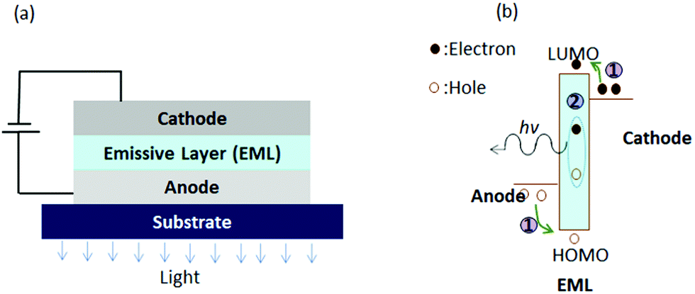 | ||
| Fig. 1 (a) Schematic of single layer OLEDs, and (b) corresponding energy level diagram. | ||
The working principle of an OLED is depicted in Fig. 1b. With applying a positive bias voltage across the electrodes, charge carriers (holes and electrons) are injected from the electrodes into the EML and travel and subsequently recombine in the EML. The recombination results in light emission with energy/color corresponding to the difference between HOMO (highest occupied molecular orbital) and LUMO (lowest unoccupied molecular orbital) energy levels of the EML.
OLEDs made with only an EML (simple structure) suffer from low performance due to the high energy barriers between the electrodes and the EML. However, by using additional layers: electron injection layer (EIL), electron transport layer (ETL), hole injection layer (HIL), and hole transport layer (HTL), shown in Fig. 2a, it is possible to create better interfaces and improve the device performances. Introduction of an EIL/HIL serves to lower the energy barrier for electron/holes when injecting from the electrodes. As a result, the OLED operational voltage is reduced, and the charge carrier density is increased. The ETL/HTL assist in creating charge balance in the EML, and function as hole/electron blocking layers to prevent charges from escaping via the opposite electrodes. The working principle of multi-layer structure OLEDs can be explained in four simple steps, Fig. 2b. Upon applying the positive bias voltage – connecting positive terminal to the anode and negative terminal to the cathode – charge carriers (electrons/hole) are pumped into the injection layers, (2) they are then injected into the transport layers, (3) this is followed by charge transport to the EML and finally, they recombine within the EML and emit light.
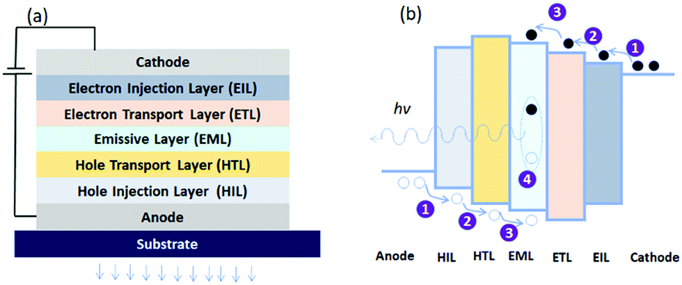 | ||
| Fig. 2 (a) Multi-layer OLEDs structure, and (b) corresponding energy level diagram. | ||
While necessary for high performance, the multi-layer OLED configuration presents significant challenges for printing/coating where each layer must be immiscible with the solvent being processed on top. Thus, for the so-called orthogonal solvent processing, developing solvent resistant films via chemistry65,66 and careful solvent selection,67–69 are both crucial research areas.
2.2 Important characteristics of OLEDs
The performance of OLEDs is commonly evaluated through measuring four optoelectronics characteristics: (1) current density (J) and luminance (L) vs. voltage, (2) current efficiency (CE), (3) external quantum efficiency (EQE), and (4) the electroluminescence spectrum (EL).70 Luminance is the amount of light emitted from or passing through an object, falling within a given solid angle. The SI unit of luminance is candela per square meter (cd m−2). The luminance and the current density are measured simultaneously at a specific applied voltage. The proportionality constant between L and J can be defined as current efficiency, see inset Fig. 3b. Examples of J–V plots, current density and luminance as a function of voltage and current efficiency against current density are shown in Fig. 3a and b.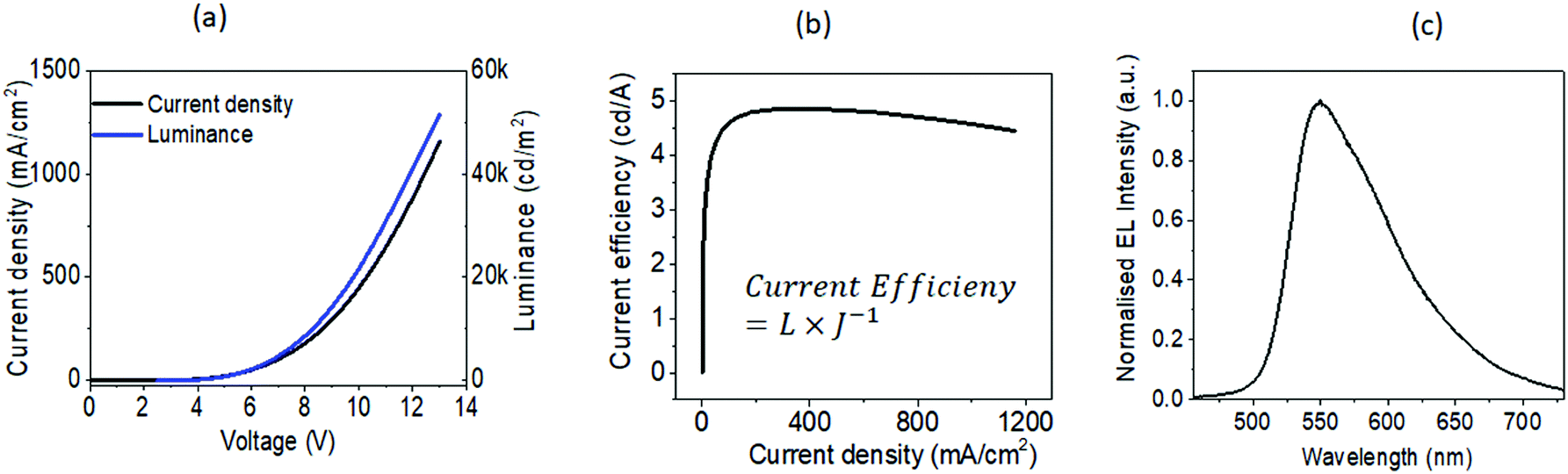 | ||
| Fig. 3 Characteristics of OLEDs: (a) current density and luminance as a function of voltage, (b) current efficiency as a function of current density, (c) EL spectrum of an OLED. All graphs are taken from our work from OLEDs (structure: glass/ITO/PEDOT:PSS/Super Yellow ((poly(para-phenylene vinylene)copolymer))/Ca/Al). | ||
Another important metric is the quantum efficiency, which consists of two parameters: external quantum efficiency (ηext) and internal quantum efficiency (ηint). The external quantum efficiency is defined as the ratio of the number of emitted photons and the injected charge carriers and is given by eqn (1),71
| ηext = χ·φf·ηST·ηout = ηint·ηout | (1) |
The first parameter, χ, represents the electrical efficiency or charge balance factor. For a well-optimized device structure this factor can reach to unity.72 The second parameter, φf, is the fraction of excitons that decay radiatively. Upon optimization of the emitter molecule this factor can also be made unity. The third parameter, ηST, account for a fraction of exciton that are able to decay radiatively because of quantum mechanics spin statistic rules. For fluorescent materials this factor can reach up to 25% and for phosphorescent or thermally activated delayed fluorescence molecule this factor can be 100%.73,74 The product of first three factors: electrical efficiency (χ), fraction of radiative decay (φf) and spin factor (ηST) gives rise to internal quantum efficiency (ηint)., which indicates the emission of photons from the emitter in the case of EL. The last parameter ηout represents the outcoupling efficiency or the fraction of photons that escapes out from the device. Reflection at the interfaces inside the OLEDs because of the difference in the refractive index between organic layers (1.6 to 1.8) and the glass (substrates, 1.5)/air (1.0) leads to confinement of majority of the photon inside the devices. Approximately only about 20 to 30% of internally generated photons escapes out from the devices, which clearly indicates that there is a large margin to improve outcoupling efficiency.75–77
Fig. 3c shows an exemplary electroluminescence spectrum, which represents the intensity of light emitted by an OLED through electroluminescence (light emission in response to the applied electric field) as a function of emitted light wavelength. From this measurement, it is possible to define the peak emission wavelength, purity of emission and the contribution from other wavelengths.70,78
2.3 Commission Internationale d’Eclairage (CIE) 1931 (x, y)
One of the tools to characterize the color of light emission is to calculate the coordinates of chromaticity where the light is represented by x and y coordinates in the 2-dimensional plane, which depicts the human eye perception. The coordinate system, a linear transformation of trichromatic based on CIE 1931 (XYZ), was created in 1931 by the Commission Internationale d’Eclairage (International Commission on Illumination).79 In this model, the relative contribution of light of wavelength (λ) is represented by X, Y, and Z, which are CIE tristimulus numbers. With a combination of these numbers, it is possible to obtain colors in all visible spectrum of light. Calculations can be made to get a specific color from the equations listed in the Fig. 4a.79,80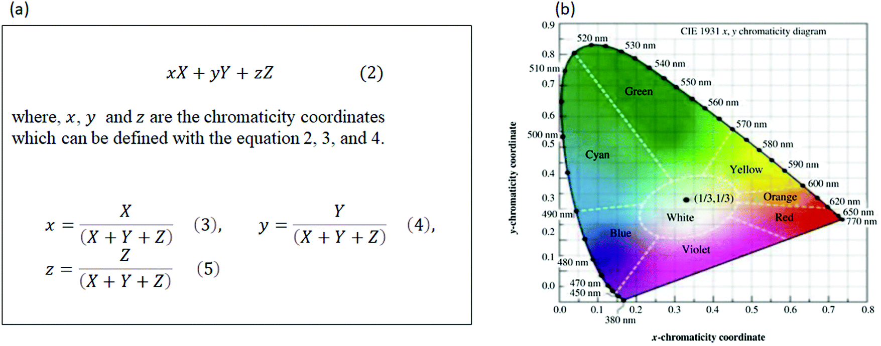 | ||
| Fig. 4 (a) Equations to calculate the color space coordinates, (b) Chromaticity diagram CIE 1931 in 2-dimension plane (reprinted with permission from the ref. 70). | ||
z can be calculated from x and y, i.e., z = 1 − x − y. Therefore, the chromaticity coordinates are represented only by two coordinates (x, y). Fig. 4b shows the chromaticity diagram CIE 1931 for a two-degree observer. Each boundary of the CIE 1931 (x,y) diagram represents the monochromatic light and using this diagram, and it is possible to compare the emission color of OLEDs or other light sources.70,81
3. Slot-die coating technique
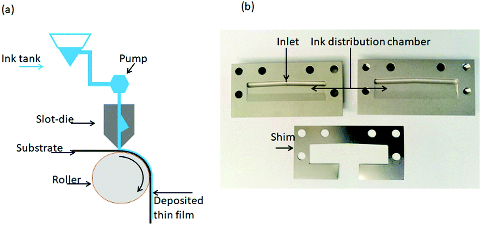
Solution coating techniques are employed to deposit uniform films of thickness varying from few nanometers to few micrometers over a large area.82 Primary coating methods used for the fabrication of organic devices are slot-die coating, blade coating, and spray coating.83 Each coating technique has its pros and cons, depending on the end application.84 For OLEDs, slot-die coating has advantages including high ink yield, closed system, and stripe patterning possibilities.A simplified schematic of the slot-die coating system is shown in Fig. 5a. Generally, there are four main parts: (a) ink reservoir, (b) pumping system, (c) slot-die head, and (d) substrate holder. The ink-reservoir is used to store the ink. In an industrial slot-die system, it is usually made from a large container; however, in small tabletop coating systems, plastic or glass syringes are used. The pumping system pumps the ink into the slot-die head at predetermined flow rates. The slot-die head comprises an ink distributor chamber and a shim, as shown in Fig. 5b. The ink distributor chamber enables uniform distribution of ink within the slot-die head and adequate flow of ink up to the opening to head. The shim defines the outlet size and is used to create a stripe pattern. Lastly, the substrate holder is used to place the substrate that is being coated. It can be a roll or flatbed type and may have heating functionality.
 | ||
| Fig. 5 (a) Schematic of slot-die coating system (reproduced with permission from ref. 83), and (b) image of slot-die components taken in our laboratory. | ||
The process of ink flow and deposition in the slot-die system is simple and straight forward. The ink stored in the container will be pumped into the slot-die head, where it distributes evenly. Eventually, it comes out from the slot-die outlet and forms a meniscus between the slot-die lip and the substrate. The meniscus moves when a slot-die head or a substrate holder moves to deposit the film on to a substrate. The film quality depends on many parameters, such as ink composition, slot-die type, and process variables (ink flow rate, coating speed, coating width, gap between the slot-die head and the substrate).85–88
The type of slot-die head shown in Fig. 5b is suitable for coating over a large area, and the shim opening determines the width of the layer. The minimum width that can be coated using such a slot-die head is in the range of centimeters. When coating low width stripes, the laterally capillary flow prevents the formation of uniform film and sharp edges. Further, the lateral capillary flow can be more intense for low viscous inks and at low coating speed. However, for some applications such as OLEDs, a well-defined stripe determines the devices’ overall performance. Fortunately, it is possible to coat high-quality stripe patterns down to micro-scale width using a dual plate (meniscus guide plate and the shim) embedded inside the slot-die head. In dual plate slot-die head, the meniscus forms between the substrate and the meniscus guide tip, instead of the slot-die lip and the substrate. Schematic of the slot-die head with meniscus guide plate and the shim plate is shown in Fig. 6.
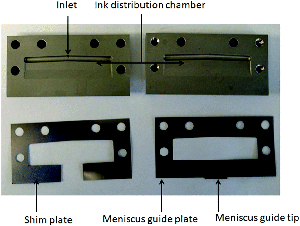 | ||
| Fig. 6 Schematic of the slot-die head with meniscus guide plate and the shim plate. Image taken in our laboratory. | ||
4. Slot-die coating of organic layers and metal electrodes
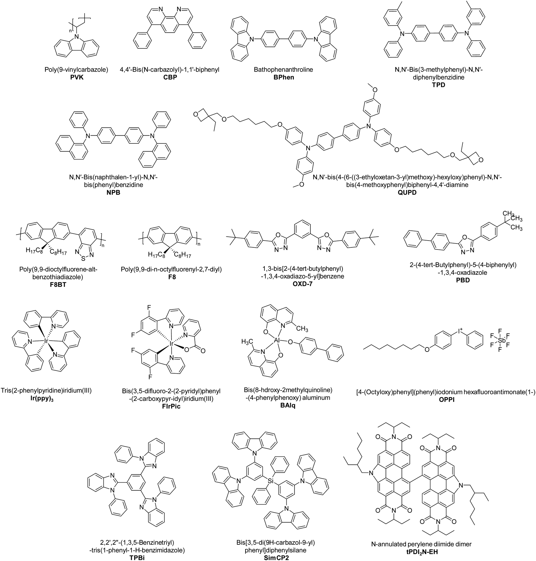
High-quality films are integral for the manufacturing the OLEDs. For fabricating efficient devices, all OLEDs layers should have precise thickness over a large area and low roughness (i.e., uniform), and be solvent resistant (to form a layer on top of it). In this section, we will discuss the quality of the films formed by the slot-die method and their impact on OLED performance, and the approaches used to coat multi-layer films. Chemical structures of all the organic materials used are shown in Fig. 26. Summary of this section is listed in Table 2.4.1 Single and bi-layer coating
Choi et al.89 reported the slot-die coating of a hybrid HTL for OLEDs with the aim of producing a pinhole-free smooth surface with efficient hole transport properties relying on a polymer to enable good film formation and a molecule to enhance hole transport. The hybrid HTL was composed of KHT-001 (Duksan Neolux Co. Ltd), and PVK (polyvinyl carbazole) in a 70![[thin space (1/6-em)]](https://www.rsc.org/images/entities/char_2009.gif) :30 ratio dissolved in chlorobenzene and toluene (3:7). The slot-die coated hybrid films showed a much smoother surface than the films coated with an only the molecule, but slightly higher than the slot-die coated polymer film. The average roughness (and peak to peak roughness) of the molecule, polymer, and hybrid layers were 122.5 nm (1070.9 nm), 0.6 nm (11.5), and 0.5 nm (0.7 nm), respectively. To compare the effectiveness of the hybrid HTL, they fabricated OLED with the configuration: glass/ITO/HTL/CBP:(Ir(ppy)3)(EML)/Bphen(HBL)/LiF/Al. Except HTL, all layers were sequentially deposited by thermal evaporation at the rate of 0.5 nm s−1. The hybrid HTL OLEDs' luminous efficiency (28.7 lm W−1) outperformed the OLEDs produced with molecule only (25.3 lm W−1) or polymer only HTL (14.6 lm W−1). Furthermore, the solvent resistance of hybrid HTL was also examined by coating PEDOT:PSS solution on top of HTL. The SEM images show, see in Fig. 7, that interface between hybrid HTL and PEDOT:PSS display clear margins when compared to the interface between SM HTL and PEDOT:PSS, suggesting that the hybrid HTL is much more robust towards the solution processed upper layer.
:30 ratio dissolved in chlorobenzene and toluene (3:7). The slot-die coated hybrid films showed a much smoother surface than the films coated with an only the molecule, but slightly higher than the slot-die coated polymer film. The average roughness (and peak to peak roughness) of the molecule, polymer, and hybrid layers were 122.5 nm (1070.9 nm), 0.6 nm (11.5), and 0.5 nm (0.7 nm), respectively. To compare the effectiveness of the hybrid HTL, they fabricated OLED with the configuration: glass/ITO/HTL/CBP:(Ir(ppy)3)(EML)/Bphen(HBL)/LiF/Al. Except HTL, all layers were sequentially deposited by thermal evaporation at the rate of 0.5 nm s−1. The hybrid HTL OLEDs' luminous efficiency (28.7 lm W−1) outperformed the OLEDs produced with molecule only (25.3 lm W−1) or polymer only HTL (14.6 lm W−1). Furthermore, the solvent resistance of hybrid HTL was also examined by coating PEDOT:PSS solution on top of HTL. The SEM images show, see in Fig. 7, that interface between hybrid HTL and PEDOT:PSS display clear margins when compared to the interface between SM HTL and PEDOT:PSS, suggesting that the hybrid HTL is much more robust towards the solution processed upper layer.
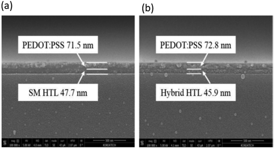 | ||
| Fig. 7 SEM image of HTL/PEDOT:PSS interface (a) small molecule HTL (b) hybrid HTL (reprinted with the permission from the ref. 89). | ||
Amruth et al.90 demonstrated the slot-die coating of bilayer: PEDOT:PSS (HTL) and F8:F8BT (EML) through the orthogonal solvents approach. Toluene was used for dissolving F8:F8BT (EML) and water for PEDOT:PSS solution (HTL/HIL). In a F8:F8BT blend system, F8 is a host, and F8BT is guest, and emission occurs only from F8BT for a well-formed film. The influence of the slot-die coating parameters: coating speed, substrate temperature, and the ink flow rate, were investigated on the quality of PEDOT:PSS and F8:F8BT film thickness. Upon optimization, they obtained the optimum coating parameters to achieved the desirable film thickness of PEDOT:PSS (34 ± 3 nm) and F8:F8BT (66 ± 5 nm) for incorporating into OLEDs. The processes of device fabrication with configuration: Glass/ITO/PEDOT:PSS/F8:F8BT/LiF/Al is shown in Fig. 8. The OLEDs made with slot-die coated films show uniform light emission with luminance and current efficiency of 357 cd m−2 and 1.7 cd A−1, respectively. Nevertheless, slot-die OLEDs failed to match the spin-coated OLEDs (1662 cd m−2 and 4.51 cd A−1) made from the same material and device structure. Besides, the EL spectrum of slot-die coated OLEDs includes a small emission peak from the host (F8) as well, suggesting a certain degree of de-mixing of F8 and F8BT. The authors believe that the significant variation of film thickness (66 ± 5 nm) and de-mixing observed in F8:F8BT films were responsible for the low performance of slot-die OLEDs. Furthermore, it was suggested that optimizing additional parameters, including the substrate, slot-die gap (i.e. film width), and ink formations (solvents and additives) could improve the performance of the slot-die OLEDs.
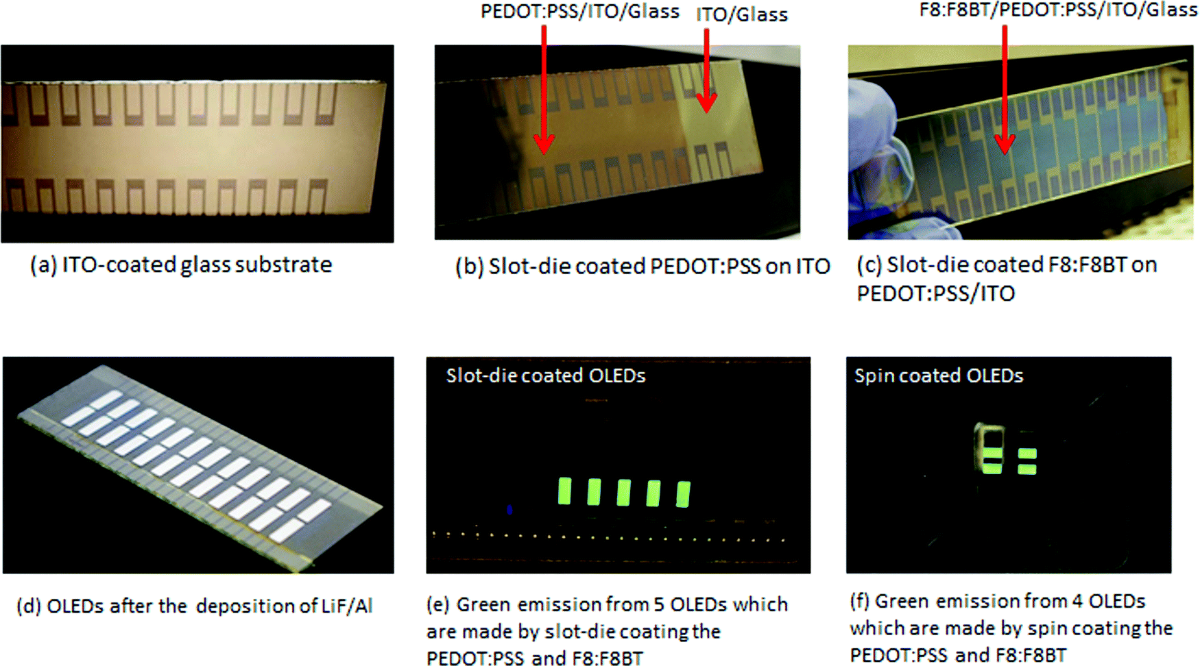 | ||
| Fig. 8 (a–d) Images showing the process for OLED fabrication. Light emission from OLEDs with (e) slot-die and (f) spin coated ETLs and EMLs (taken from the ref. 90). | ||
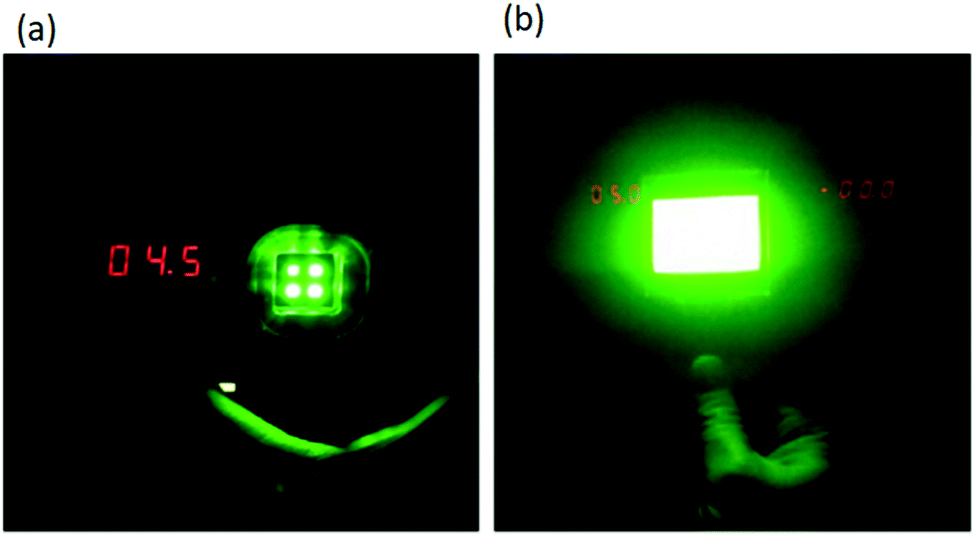
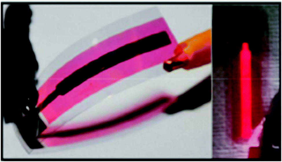
Dayneko et al.91 investigated the utility of the N-annulated perylene diimide fluorophore (tPDI2N-EH) as a red emitting material for OLED applications and demonstrated the slot-die coating (via a roll process) of bilayer OLEDs on a flexible plastic substrate. The OLED configuration was: PET(Polyethylene terephthalate)/ITO/PEDOT:PSS/F8:tPDI2N-EH/LiF/Ag. The PEDOT:PSS (HTL) dissolved in water and F8:tPDI2N-EH (EML) dissolved in toluene were sequentially slot-die coated using the orthogonal solvents approach on top of ITO coated PET substrates. LiF/Ag was thermal evaporated, as the cathode system, to complete OLED fabrication. Blending of tPDI2N-EH with F8 was found to improve electrical properties of the OLEDs owing to efficient Förster resonance energy transfer from F8 to tPDI2N-EH. The slot-die coating of large-area OLEDs (160 mm2) shows uniform light emission (Fig. 9) with turn-on voltage and maximum luminance of 6.6 V and 1.1 cd m−2, respectively. However, slot-die OLEDs’ performance is much lower than the spin-coated OLEDs (turn-on voltage: 2.6 V and max. luminance: 435 cd m−2). The authors suggest that the modification of tPDI2N-EH to achieve efficient PLQY and further optimize the slot-die coating parameters is possible to increase the OLEDs performance.
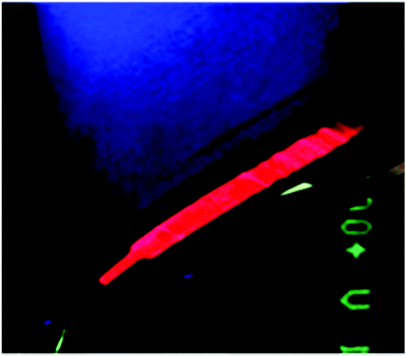 | ||
| Fig. 9 Image of a flexible OLED with slot-die coated HTL (PEDOT:PSS) and EML (F8:tPDI2N-EH) under operation and emitting red light (taken from the ref. 91). | ||
Abbel et al.92 presented the slot-die coating (via a roll-to-roll (R2R) process) of the HIL and EML using orthogonal solvents approach on a flexible PET substrate. Further, as a reference, OLEDs were also fabricated by sheet-to-sheet (S2S) slot-die coating technique under an inert atmosphere. Here, commercially available solutions were used: HIL, XA-3215 supplied from Plexcore (Pittsburgh, Pennsylvania), and EML, G13017X supplied from Sumitomo Chemical Co., Ltd, Osaka, Japan. The R2R coating of both functional layers was created in a highly controlled manner to obtain desirable film width and thickness. All films were uniform except some mottle effect observed on the HIL surface. The fabrication of OLEDs was completed with the configuration: PET/ITO/HIL/EML/Ba/Al. The R2R coated OLEDs showed a brightness of 100 cd m−2 (at 5 to 6 V), which is only 10% the brightness of the S2S OLEDs (ca. 1000 cd m−2 (at 5 to 6 V)). On the other hand, both the R2R and S2S manufactured OLEDs showed similar current efficiency between 5 to 7 cd A−1. The lifetime of the S2S manufactured OLEDs was far superior to that of R2R manufactured OLEDs. The surface of the latter was investigated through thermal and optical imaging which revealed bright spots and dust particles (Fig. 10) attributed to contamination since the OLED layers were coated on the benchtop. It was suggested that the presence of bright spot under electrical input and dust particles are responsible for the degradation of R2R manufactured OLEDs performance and as such raises the question, can high performance OLEDs be fabricated outside of a controlled environment?
 | ||
| Fig. 10 (a) Image of an OLED with slot-die coated HIL/EML. (b) Overlay of lock-in IR imaging at a bias voltage of 2 V (c) and optical image of dust particle of the slot-die coated OLEDs (reprinted with the permission from the ref. 92). | ||
Raupp et al.93 investigated the fabrication of OLEDs (configuration: Glass/ITO/PEDOT:PSS/EML/LiF/Al) with the HIL and EML slot-die coated. LiF (1.3 nm) and Al (100 nm) were deposited by thermal evaporation process. The PEDOT:PSS solution was blended with ethanol before coating to increase the wetting of the patterned ITO surface. For the EML, five materials were evaluated: F8BT (dissolved in toluene), CBP:Ir(ppy)3 binary blend (dissolved in chloroform), PVK:Ir(ppy)3 binary blend (dissolved in chlorobenzene), PVK:OXD-7:Ir(ppy)3 ternary blend (dissolved in chlorobenzene), and PVK:TPD:PBD:Ir(ppy)3 quaternary blend (dissolved in chlorobenzene) (see Fig. 26 for structures and names). Light emission from the five OLEDs is shown in Fig. 11. The standard deviation of film thickness of F8BT and PVK:TPD:PBD: Ir(ppy)3 was ±15%, and for other films, it was below 10%. The best OLED performance came from using the PVK:OXD-7:Ir(ppy)3 ternary blend as the EML. Current efficiency and luminance were 5 cd A−1 and 10000 cd m−2, respectively, attributed to a well-balanced charge mobility. Lowest performing OLEDs had PVK:Ir(ppy)3 binary blend EMLs. The low performance was attributed to a mis-matched charge mobility. Concerning the standard deviation of the device parameters: current density, brightness, luminous and current efficiency, the OLEDs with PVK:TPD:PBD:Ir(ppy)3 as the EML have shown the lowest (21%). For the rest of the OLEDs, the standard deviation is between 25 to 60%. The high standard deviation highlights the major challenge of slot-die coated OLEDs for achieving consistent uniform film formations.
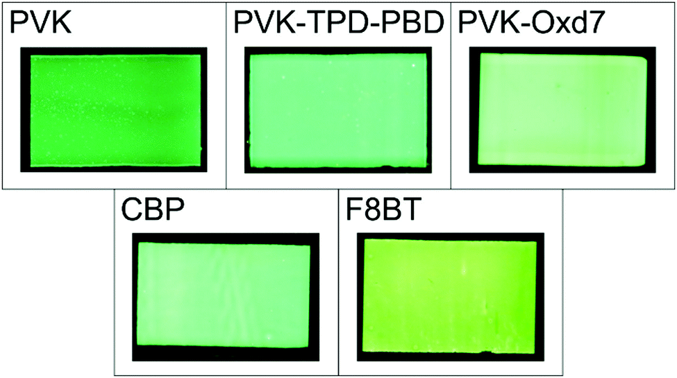 | ||
| Fig. 11 Light emission from five OLEDs composed of different EML. (reprinted with the permission from the ref. 93). | ||
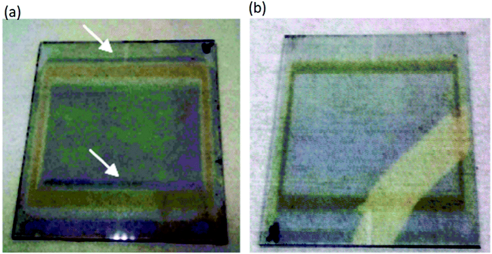
Choi et al.94 fabricated OLEDs with a structure of: glass/ITO/PEDOT:PSS/KHT-001/CBP:Ir(ppy)3/Bphen/LG201/LiF/Al where the PEDOT:PSS (HIL) and HTL (KHT-001) layers were formed using slot-die coating. They addressed three issues: (1) flow down of PEDOT:PSS solution near the insulator bank edge, (2) pinhole formation in small molecule (KHT-001) film, and (3) dissolution issue that takes place at the interface of the HIL and HTL. First, it was found that the PEDOT:PSS films coated on top of ITO coated substrate (which consists of an insulator bank) become thicker just after coating near the edge of the insulator bank due to backflow of the PEDOT:PSS solution. This problem was addressed by adding a small amount of fluoro-based surfactant (a wetting agent) into the PEDOT:PSS solution and the coating bed temperature was raised to 80 °C to speed up the evaporation rate of solvent. Fig. 12 shows the slot-die coated PEDOT:PSS films before and after solving the edge issue. Second, the KHT-001 molecule was dissolved in toluene or chlorobenzene and was coated on top of the HIL. Unfortunately, the films contained pinholes, which can result in short-circuited OLEDs. Such an effect was eliminated by using the solvent mixture instead of using a single solvent. This HTL film coated from a toluene:chlorobenzene (30:70) mixture leads to smooth films with RMS roughness value of 0.4–0.6 nm, and thus eliminated the pinholes. Third, it was observed that the coating of the HTL on the HIL leads to the formation of bubble-like patterns and slightly degraded the quality of the HTL layer. This problem was mitigated by reducing the flow rate of the ink during the coating process. After addressing all three problems, OLEDs were fabricated with both the slot-die coated HIL and HTL. The emission of light from slot-die OLEDs is shown in Fig. 13. Furthermore, as a reference, OLEDs with the spin-coated HIL and vacuum evaporated HTL were also produced. The power efficiency of the slot-die OLEDs and reference OLEDs at 1000 c m−2 were 27.2 lm W−1 and 25.5 lm W−1, respectively. Noteworthy is that after optimizing the slot-die coating conditions and obtaining uniform multi-layers, the performance of the OLEDs with slot-die coated layers matched that of the OLEDs with spin-coated layers.
 | ||
| Fig. 12 Image of PEDOT:PSS film coated on ITO (a) without and (b) with fluorosurfactant (reproduced with permission from the ref. 94). | ||
 | ||
| Fig. 13 Emission of green light from (a) small area (2 mm × 2 mm) and (b) large area (43 mm × 29 mm) slot-die coated OLEDs (reproduced with permission from the ref. 94). | ||
Parkr et al.18 optimized the slot-die coating parameters for coating the HIL and EML and demonstrated high efficient OLEDs in an ambient conditions. They used the device configuration: glass/ITO/HIL/EML/Cs2CO3/Al where the HIL was PEDOT:PSS (in water and isopropyl alcohol in 1:3 ratios) and the EML was a ternary blend of PVK:TPD:PBD:Ir(ppy)3 (dissolved in a solvent mixture of 1,2-dichloroethane and chloroform in the ratios 3:1). The influence of slot-die coating parameters (coating speed and the slot-die gap height) on film thickness was examined. The results show that the films thickness increases at higher coating speeds and gap heights. The optimized HIL and EML films were smooth, having a low RMS roughness of ca. 1.1 nm. Films were compared to those formed by the spin coating technique. Impressively, the OLEDs with slot-die coated layers outperformed the OLEDs with spin-coated layers. The maximum luminance and the maximum current efficiency were 50000 cd m−2 and 29 cd A−1, respectively, for the OLEDs with slot-die coated layers, and 36000 cd m−2 and 22.2 cd A−1, respectively for OLEDs with spin-coating active layers. Better charge injection and transport was responsible for the improved performance. Large area OLEDs were fabricated (Fig. 14) with the emission intensity nearly equal among of the devices confirming the uniform HIL and EML film formation using slot-die coating. Combined with all the prior art suggest that the slot-die coating is a viable method to fabricate OLEDs so long as care is given to forming uniform films.
 | ||
| Fig. 14 Picture of nine OLEDs pixel under voltage bias of 10 V on a glass substrate 5 × 5 cm2 (take from the ref. 18). | ||
4.2 Triple and quadruple layer coating
Raupp et al.43 addressed the fundamental challenges involved in the coating of a multi-layer stack for OLED application. OLEDs with a device structure of glass/ITO/HIL/EML/ETL/LiF/Al were investigated, where all the three layers: PEDOT:PSS (HIL), SimCP2:FIrPic (EML) and TPBi (ETL) were slot-die coated. Critically, they investigated the feasibility of coating a molecular film (TPBi) on top of another molecular film. To check the impact of the solvent on the quality of TPBi film formation (ETL), three solutions of TPBi were prepared in methanol (MeOH), methanol:acetic acid (MEOH:AA) and 1-propanol:formic acid (1-Prop:FA). The RMS roughness of the slot-die coated PEDOT:PSS and SimCP2:FIrCP2 films were as low as 0.79 nm and 0.38, respectively. The RMS roughness of TPBi films coated from MeOH:AA (0.66 nm) was half of that of TPBi films cast from MeOH (1.3 nm). Unfortunately, the roughness of TPBi coated from 1-Prop:FA was not measured due to the formation of pinholes across the films. The AFM images of all these films are shown in Fig. 15. The OLEDs with TPBi coated from MeOH:AA show the best performance with the current efficiency of 2.02 cd A−1. On the other hand, the efficiency of OLEDs with TPBi cast from MeOH and 1-Prop:FA was 0.39 cd A−1 and 0.16 cd A−1, respectively. Further, the luminance for the OLEDs where TPBi cast from MeOH:AA was higher than that of the other two OLEDs. The drop in efficiency for these two devices is due to the slight intermixing of the HIL and EML layer. Furthermore, to compare the influence of the third layer (TPBi), the two-layer OLEDs were fabricated by eliminating the TPBi film. The low CE (0.061 cd A−1) of two layers OLEDs clearly shows that the TPBi layer is need for good OLED performance.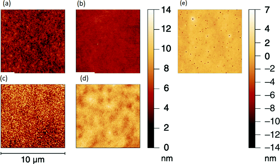 | ||
| Fig. 15 AFM images of (a) PEDOT:PSS (b) SimCP2:FIrCP2 (c) TPBi from MeOH (d) TPBi from MeOH–AA and (e) TPBi from 1-Prop–FA (reprinted with permission from the ref. 43). | ||
Merklein et al.95 demonstrated OLEDs with four organic layers slot-die coated. Such a feat was accomplished by combining cross-linkable materials and the orthogonal solvents approach. Fig. 16 shows the OLED structure schematic, where the HTL on HIL and ETL on EML formed with an orthogonal solvent approach, and the EML on HTL created with a crosslinking approach. The HTL was blended with (4-Octyloxyphenyl)phenyliodonium hexafluoroantimonate (OPPI) to initialize crosslinking using UV light. The RMS roughness for the HIL, crosslinked HTL, EML and ETL were 0.74 nm, 0.21 nm, 0.21 nm, and 0.25 nm, respectively, which confirmed the uniform film formation. Four types of OLEDs were fabricated to investigate each layer, which layers were added in between the anode (glass/ITO) and cathode (LiF/Al) to build up the devices: (1) two-layer OLEDs (HIL and EML), (2) three-layer OLEDs (HIL, crosslinked-HTL and EML) and (3,4) two four-layers OLEDs, one with the crosslinked HTL and another without the crosslinked HTL. The results show that the OLED performance improves with more layers. Further it was shown that the OLEDs with four layers without crosslinking the HTL gave poor performance due to intermixing of the EML and HTL. The average power efficiency of three-layer OLEDs increased by a factor of 1.7 compared to the one for two-layer OLEDs, and the average power efficiency of four-layer OLEDs increased by a factor of 2.2 compared to the one for the three-layer OLEDs. Thus, the author suggests that the use of multilayer structures and combination of crosslinking and orthogonal solvent approach for multilayer film formation should assist in achieving highly efficient OLEDs.
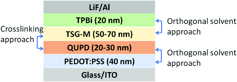 | ||
| Fig. 16 Schematic of OLEDs structure with four organic layers. QUPD is N,N-bis(4-(6-((3-ethyloxetan-3-yl)methoxy)hexyloxy)phenyl)-N,N-bis(4-methoxyphenyl)biphenyl-4,4-diamine, TSG-M is green emitter. (reproduced from the ref. 95). | ||
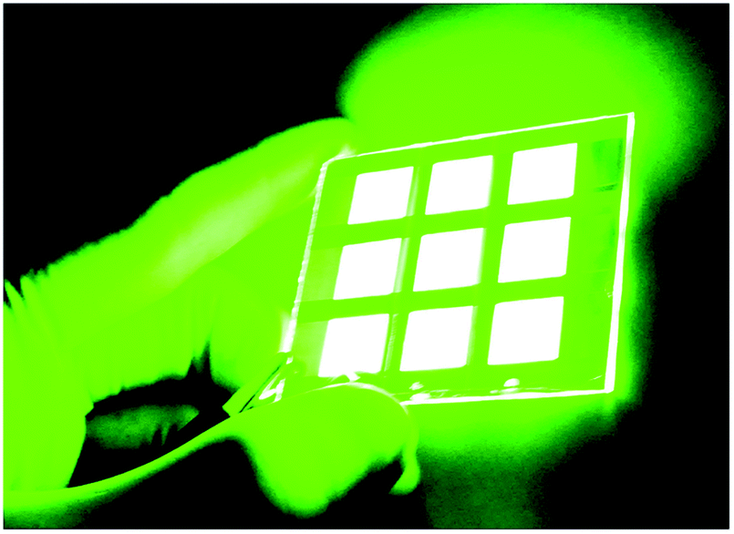
Rahmati et al.42 presented the slot-die coating of four organic layers for the fabrication of flexible red OLEDs. The OLED structure consisted of: PET/ITO/PEDOT:PSS/PVK/PFO:tPDI2NEH/ZnO/Ag. The four slot-die coated layers included PEDOT:PSS as the HIL, PVK as the HTL, red emitting blend PFO:tPDI2NEH as the EML, and ZnO at the ETL (zinc oxide in form of nanoparticles). Here the orthogonal solvent approach was solely used. Importantly, no chlorinated solvents were used for processing of any layers. The RMS roughness of the slot-die coated PEDOT:PSS (0.45 nm), PVK (0.17 nm), and ZnO (0.85 nm) films was excellent, again indicating uniform film formation, and thus suitable for device operation. The OLEDs were slot-die coated in strips with a large active area of 160 mm2 and exhibited homogeneous emission, as show in Fig. 17, further highlighting the usefulness of this processing method. Utility of the PVK and ZnO was critical on achieving high performance. The results (see Table 1) show that the OLEDs with PVK and ZnO offer the best results, owing to efficient charge balance, with low turn-on voltage of 2.8 V, highest luminance of 303 cd m−2, and highest CE of 0.74 cd A−1.
 | ||
| Fig. 17 Image of slot-die coated flexible OLEDs (left) without bias voltage (right) red light emission with bias voltage (reprinted with the permission from the ref. 42). | ||
| Device architecture | Turn-on voltage (V) | Luminance (cd m−2) | CE (cd A−1) | PE (lm W−1) | EQE (%) |
|---|---|---|---|---|---|
| PET/ITO/PEDOT:PSS/EML/LiF/Ag | 5.0 | 3.89 | 0.010 | 0.004 | 0.01 |
| PET/ITO/PEDOT:PSS/PVK/EML/LiF/Ag | 5.0 | 14.0 | 0.017 | 0.006 | 0.03 |
| PET/ITO/PEDOT:PSS/PVK/EML/ZnO/Ag | 2.8 | 303.0 | 0.740 | 0.291 | 0.11 |
| Device structure | No. of slot-die layers | Slot-die coated layers | Performance of slot-die OLEDs | Ref. |
|---|---|---|---|---|
| C.E.: current efficiency, P.E.: power efficiency, B: brightness, Ton: turn on voltage | ||||
| Glass/ITO/HTL/CBP:(Ir(ppy)3) (EML)/Bphen(HBL)/LiF/Al | One | HTL: (PVK:KHT-001, 30:70) dissolved in in chlorobenzene and toluene (3:7) |
P.E.: 28.7 lm W−1 | 89 |
| Glass/ITO/PEDOT:PSS(HIL)/F8:F8BT(EML)/LiF/Al | Two | PEDOT:PSS in water, F8:F8BT dissolved in toluene | B: 357 cd m−2 and C.E: 1.7 cd A−1 | 90 |
| PET/ITO/PEDOT:PSS(HIL)/F8:tPDI2N-EH(EML)/LiF/Ag | Two | PEDOT:PSS in water, F8:tPDI2N-EH dissolved in toluene | T on: 2.6 V, B: 435 cd m−2 | 91 |
| PET/ITO/XA-3215(HIL)/G13017X (EML)/Ba/Al | Two | XA-3215 dissolved in a non-aqueous polar solvent, G13017X dissolved in o-xylene | R2R OLEDs (B: 100 cd m−2 and C.E.: 5 to 7 cd A−1), S2S OLEDs (B: 1000 cd m−2 and C.E.: 5 to 7 cd A−1) | 92 |
| Glass/ITO/PEDOT:PSS(HIL)/EML/LiF/Al, EML: (1) F8BT, (2) CBP:Ir(ppy)3, (3) PVK:Ir(ppy)3, (4) PVK:OXD-7:Ir(ppy)3, and (5) PVK:TPD:PBD:Ir(ppy)3 | Two | PEDOT:PSS in water and ethanol, F8BT dissolved in toluene, CBP:Ir(ppy)3 dissolved in chloroform, PVK:Ir(ppy)3 dissolved in chlorobenzene, PVK:OXD-7:Ir(ppy)3 dissolved in chlorobenzene, PVK:TPD:PBD:Ir(ppy)3 dissolved in chlorobenzene | OLEDs with EML: F8BT (B: 300 cd m−2 and C.E: 0.1 cd A−1), CBP:Ir(ppy)3 (B: 250 cd m−2 and C.E: 0.4 cd A−1), PVK:Ir(ppy)3 (B: 50 cd m−2 and C.E: 0.3 cd A−1), PVK:OXD-7:Ir(ppy)3 (B: 2000 cd m−2 and C.E: 1.8 cd A−1), PVK:TPD:PBD:Ir(ppy)3 (B: 5000 cd m−2 and C.E: 5 cd A−1) | 93 |
| Glass/ITO/PEDOT:PSS (HIL)/KHT001(HTL)/CBP:Ir(ppy)3(EML)/Bphen(HBL)/LG201(ETL)/LiF/Al | Two | PEDOT:PSS dissolved in water, KHT-001 (solution) | P.E: 27.2 lm W−1 at 100 cd m−2 | 94 |
| Glass/ITO/PEDOT:PSS(HIL)/PVK:TPD:PBD:Ir(ppy)3(EML)/Cs2CO3/Al | Two | PEDOT:PSS dissolved in water and isopropyl alcohol (1:3), PVK:TPD:PBD:Ir(ppy)3 dissolved in 1,2-dichloroethane and chloroform (3:1) |
B: 50000 cd m−2 and C.E.: 29 cd A−1 |
18 |
| Glass/ITO/PEDOT:PSS(HIL/SimCP2:FIrPicEML)/TPBi(ETL)/LiF/Al | Three | PEDOT:PSS in water:1-propanol (40 vol%):TritonX (1.9 × 10⁻⁶ wt%), SimCP2:FIrPic dissolved in toluene, TPBi dissolved in MeOH or MeOH:acetic acid or 1-propanol:formic acid | C.E.: 2.02 cd A−1 | 43 |
| Glass/ITO/PEDOT:PSS(HIL)/QUPD(HTL)/TSG-M(EML)/TPBi(ETL)/LiF/Al | Four | PEDOT:PSS in water:1-propanol:TritonX (10−6 wt%), QUPD 2 wt% of the photoacid OPPI in toluene, TSG-M dissolved in toluene, TPBi dissolved in methanol:AA | C.E.: 8 cd A−1 and P.E.: 3.5 lm W−1 | 95 |
| PET/ITO/PEDOT:PSS(HIL)/PVK(HTL)/PFO:tPDI2NEH(EML)/ZnO(ETL)/Ag | Four | PEDOT:PSS in water, PVK dissolved in toluene, PFO:tPDI2NEH dissolved in o-xylene, ZnO in methanol | T on: 2.8 V, B: 303 cd m−2, C.E.: 0.7 cd A−1 | 42 |
4.3 Coating of metal electrodes
In addition to the semiconducting layers, highly conducting films/metal electrodes are equally crucial for realizing highly efficient, flexible, and long lifetime OLEDs. Slot-die coated metal electrode has been used in various organic devices such as photovoltaics,96,97 sensors,98 and touch panels.99,100 However, it is essential to mention that there has been little progress in examining the slot-die coated anode/cathode for OLED applications.Mühl et al.101 examined the slot-die coating of silver nanowire as an anode for the fabrication of large-area OLEDs. The OLED structure was Ag NWs (anode)/HIL/HTL/EBL/EML/HBL/ETL/Al (cathode), with exact materials not disclosed. At first, coating of silver nanowire was optimized to obtain low sheet resistance by choosing the best possible coating parameters: ink flow rate (8 μl s−1), coating speed (5 mm s−1), and the substrate-slot-die lip gap height (80 μm). The AFM image of a silver nano wire film is shown in Fig. 18. After optimization, multi-layer OLEDs with a silver nanowire film as the anode were constructed. The OLEDs were fabricated on two kinds of Ag nanowire coated substrates. In the first substrate, the flow of current is in parallel to the nanowire orientation, and in the second, the flow of current is perpendicular to the orientation of nanowire. The sheet resistance of perpendicularly oriented nanowire films (70 Ω sq−1) was twice when compared to the sheet resistance of parallel oriented nanowire films. It was reported that both OLEDs show comparable luminous uniformity. However, the uniformity of the current density in parallel oriented nanowire films was much better than the perpendicular oriented nanowire films.
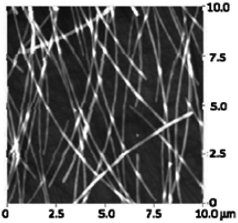 | ||
| Fig. 18 AFM image of silver nanowire film (taken from the ref. 101). | ||
5. Slot-die coating on pixel bank layer
Commonly, the slot-die coating process can be used to create large-area organic films. Such a large-area coating could be used to manufacture OLEDs lighting, where pixel formation is not necessary. However, we found that there has been progress in using the slot-die coating in the fabrication of the display panel.Shin et al.102 studied the slot-die coating of organic films on a pixel bank layer, with the insulating film consisting of micro sized opening that defines OLEDs size. The pixel bank with sizes 20 × 60 μm and 75 × 180 μm are shown in Fig. 19a and b and are formed using photo resistive materials on an ITO coated glass substrate. The influence of the bank size and the drying situation (with atmospheric and partial vacuum condition) on the film growth of PEDOT:PSS (aqueous solution) and PVK (dissolved in ethyl benzoate, a non-aqueous solvent) were the focus of this study. The PEDOT:PSS films, when coated on pixel bank, result in a concave shape profile, meaning that the thickness is higher at the edge than in the center. Furthermore, such a profile appears irrespective of pixel bank size. The author considers that such a profile could be the result of capillary action that arises near the wall of the bank. However, as the bank size grows, the overall film thickness increases, because the larger pixel facilitates the flow of a large amount of ink into the cell. The second parameter, drying condition, shows an insignificant influence on the PEDOT:PSS film formations as the solvent evaporates instantly during the coating or just after the coating. On the other hand, similar to the PEDOT:PSS layer, the PVK films also result in a concave-shaped film irrespective of the pixel bank size. Nevertheless, unlike PEDOT:PSS, the drying condition assists to suppress the concave shape profile. As depicted in Fig. 19c and d, under the partial vacuum condition, the evaporation rate increases at the center compared to the edge. The difference in the evaporation rate enables convective from edge to the center, which results in an increase in the uniformity of the films. Importantly, the convective flow shall only come into effect with the use of a higher boiling point solvent. Since the PVK ink is composed of a solvent with high boiling point (ca. 213 °C) the convective flow was useful for suppressing the edge thickness. Conversely, the PEDOT:PSS dissolved in water (bp = ca. 100 °C), dried faster before the occurrence of the convective flow. Finally, the phosphorescent green OLED panel was fabricated on bank structure. The OLEDs (configuration: ITO/PEDOT:PSS(HIL)/PVK(HTL)/CBP:Ir(ppy)3(EML)/Bphen(HBL)/LG201(ETL)/LiF/Al) fabricated with the PVK films formed under partial vacuum have shown uniform emission due to pronounced film homogeneity compared to the OLEDs made with PVK film dried in atmospheric condition. Images of emission from OLEDs are shown in Fig. 20a and b.
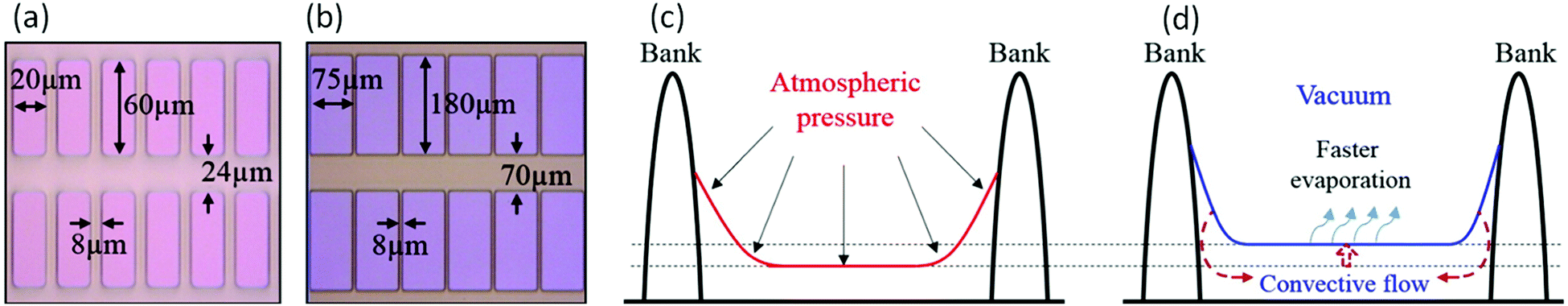 | ||
| Fig. 19 Image of patterned pixel bank of size (a) 20 × 60 μm and 75 × 180 μm (b) 20 × 60 μm and 75 × 180 μm. Schematic view of film formation process under (c) atmospheric pressure and (d) partial vacuum (reprinted with permission from the ref. 102). | ||
 | ||
| Fig. 20 Image of light emission from the OLEDs pixel (75 × 180 μm) where slot-die coated PVK annealed under (a) atmospheric pressure and (b) partial vacuum (reprinted with permission from the ref. 102). | ||
In parallel, the same research group demonstrated a way to improve the thickness uniformity of the PEDOT:PSS layer.103 The film homogeneity was enhanced by dilution of PEDOT:PSS with DI water and pre-drying under the vacuum or head conduction (raising coating bed/hot plate temperature). The pre-drying alone has a negligible effect on improving the uniformity of the film. Although the heat conduction has marginally improved, it is not good enough for AMOLED (Active Matrix OLED) applications. When the pure PEDOT:PSS solution was mixed with DI water, the film uniformity was found to significantly improved with vacuum pre-drying or heat conduction. The main idea behind diluting the PEDOT:PSS is to reduce the evaporation rate of solvent in the wet films and thereby, the solution has sufficient time for the convective flow from edge to center during the pre-drying process. On top of this, the heat conduction was found to be much better than vacuum pre-drying, and this is evident from the aperture ratio, which is the percentage of emitted area in the pixel. The aperture ratios of OLEDs made with vacuum pre-dried PEDOT:PSS films and heat conduction were measured to be 48% and 70%, respectively.
6. Micro-tip slot-die: towards eliminating pixel bank structure
In the previous sections, we saw the application of the slot-die technique for OLED displays. However, it should be noted that the slot-die method has been used to coat only large-area films, not the micro-sized pixels. To produce high-density RGB OLED pixels, the formation of micro-sized stripes of ∼100 μm is necessary. Although stripe coating is possible, for example, used to fabricate solar cells, the stripe width is usually on the order of centimeter, which is too large for high-resolution displays. Thus, high-resolution printing techniques such as inkjet are often employed for the fabrication of OLED displays.Nevertheless, recently, a few reports have shown how slot-die coating can be used to create micro-sized films for AMOLED applications. In such a slot-die coating system, designing of the micro-sized tip on a meniscus guide plate plays a critical role. One of the significant advantages of this slot-die coating system is that it eliminates the need for pixel bank patterns. Moreover, it promises the manufacturing of high-density OLEDs panel solely by slot-die coating technique.
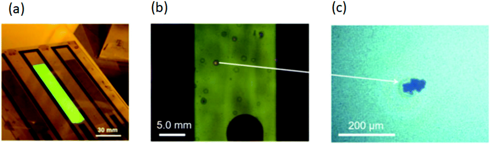
Kim et al.104 has studied the design of the meniscus guide plate to form a micro-sized PEDOT:PSS stripe for AMOLED applications. To achieve the high-quality PEDOT:PSS stripes, the process variables: (1) coating speed, (2) the dual plate parameters: μ-tip width, shim plate, and the thickness μ-tip length, and (3) the ink parameter: viscosity was carefully optimized. They found that the increase in the coating speed resulted in a drop in the stripe width and thickness. Reducing the shim width from 250 μm to 80 μm decreases the stripe width; but, increases the stripe thickness because of the same volume of ink being dispensed. Another meniscus guide parameter, the μ-tip length, significantly influences the fluid distribution at the tip and near the head lip. When the μ-tip was extended, more fluid distributes near the head lip than at the tip. Conversely, for shortened the μ-tip, more fluid circulates at the tip than near the head lip. After optimizing, they concluded that the thin shim, shortened and narrow μ-tip, and a high coating speed provide excellent μ-stripe. Besides, the viscosity of the PEDOT:PSS, an ink parameter, significantly alters the film thickness; as it rises, the film gets thicker. Subsequently, the coating of densely packed PEDOT:PSS stripe with an average thickness of 103 nm and a 168 μm was successfully demonstrated. In addition to the aqueous ink (PEDOT:PSS), the coating of the non- aqueous ink (PVK) was also optimized for the best quality film. Eventually, to demonstrate the feasibility of the slot-die coated stripe, 168 μm micro sized OLEDs were fabricated using PEDOD:PSS stripes as anode/HTL. Although this study has successfully shown the possibility of a coating micro-sized stripe, the 168 μm wide stripe is still significant, because the RGB OLED display applications prefer 100 μm wide stripes.
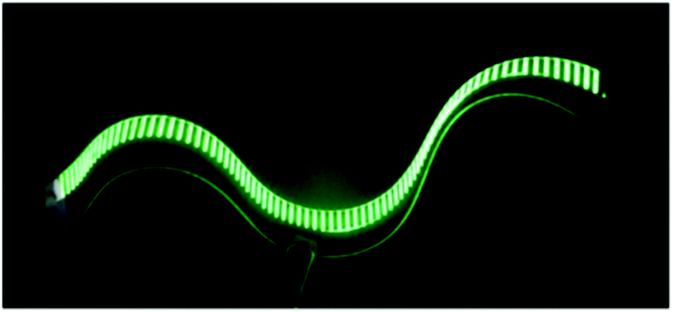
Lee et al.105 demonstrated stripes width of under 100 μm. They achieved such narrow stripes by suppressing the lateral capillary flow that shows up in a slot-die head lip. The capillary flow arises due to the adhesive force between the ink and the solid surface (head lip). Therefore, to suppress the capillary flow, both the meniscus guide's tip and the head lip were made hydrophobic. The head lip was made hydrophobic by coating with Teflon materials. Because of difficulty in coating the Teflon, the hydrophobic meniscus guide tips were made by making micro grove structures on its surface. A well-optimized micro grove patterns whose width, clearance, and depth are 50 μm, 50 μm, and 10 μm, respectively. To demonstrate, the RGB OLEDs (5 cm long and 800 μm wide) were fabricated on PET substrate using a narrow stripe of PEDOT:PSS as an anode. The red, green, and blue OLEDs show homogeneous emission with a peak intensity of 620, 520, and 472 nm. These results suggest the potential application of slot-die coating for the fabrication of high-resolution OLEDs and can be to make other organic devices or electrodes.
Kim et al.106 examined the impact of the scratches over slot-die head on the quality of PEDOT:PSS stripe. For the study purpose, they have chosen two similar slot-die heads; one (Head A) that has a scratch, and another (Head B) free from scratch. The optical images and the surface profile of the both heads are shown in Fig. 21. For Head A, it was found that the maximum coating speed significantly reduced when compared to Head B. As an example, for Head A, the maximum coating speed reaches only up to 7 mm s−1 for building 50 stripes, whereas, for Head B, the speed can reach up to 20 mm s−1. Such a difference is due to the unstable ink flow in the slit channel in the presence of scratches. Moreover, because of low coating speed, when use of Head A, the thickness and the width of stripes are relatively high, consequently diminishing the inter-stripe width. Furthermore, when the number of stripes increases to 100, it was found that the probability of line break-up was high for both the heads because as the outlets' numbers increase, the unevenness of the pressure distribution inside the cavity raises. However, for the case of Head B, it is possible to coat 25, 50 and 100 stripes without any problem upon modifying other coating parameters. Even a coating of 150 stripes at the maximum coating speed of 20 mm s−1 was also successfully demonstrated. Unfortunately, with Head A, it was possible to demonstrate only 25 and 50 stripes. This study suggests that the presence of scratch in the slot-die head limits the speed of coating, stripe density, and the number stripes. Finally, to demonstrate, the green OLEDs were fabricated using Head B with 150 stripes on a PET substrate.
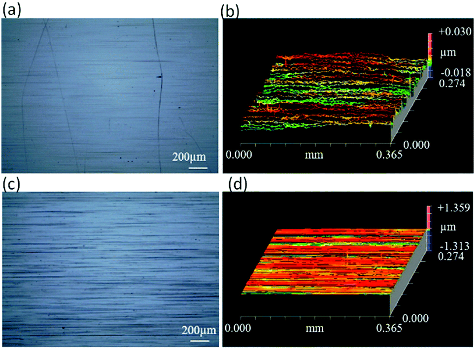 | ||
| Fig. 21 Surface of head A's (a) optical image and (b) its surface profile. Surface of head B's (c) optical image and (d) its surface profile (reprinted with the permission from the ref. 106). | ||
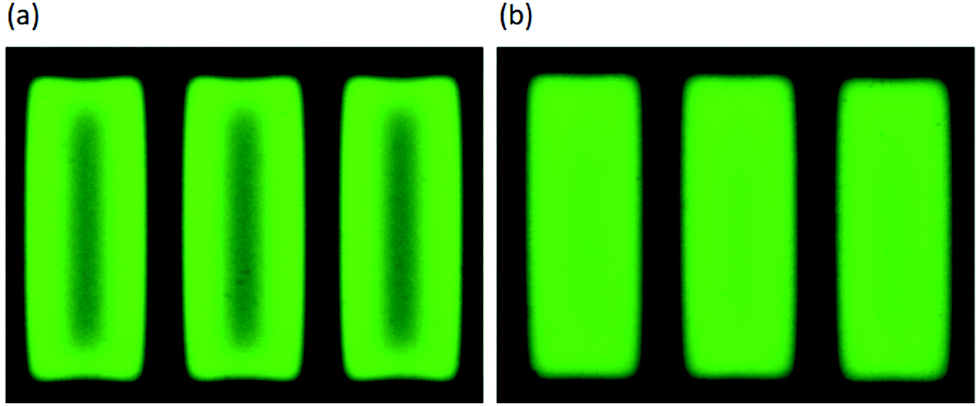
The formation of a uniform layer is a crucial step for achieving high-performance solution-based OLEDs. In pursuance of that Lee et al.107 showed the pre-drying could significantly help in the planarization of bilayer: PEDOT:PSS and PVK. It was also demonstrated that the OLEDs with a planarized layer exhibit better performance than the OLEDs with a non-planarized layer. In the interest of knowing the optimum pre-drying temperature, the PEDOT:PSS was coated at different pre-drying temperatures: 20 °C, 40 °C, 50 °C and 60 °C. It was found that at the temperature of 40 °C, the PEDOT:PSS stripes become planarized, as shown in Fig. 22. Similarly, the PVK films become planarized at a pre-drying temperature of 65 °C. To demonstrate the result of planarization, they have fabricated two kinds of OLEDs. One with planarized PEDOT:PSS/PVK layer and another with a non-planarized layer (as a reference device). The OLEDs made with planarized OLEDs have shown uniform emission. While emission from the non-planarized layers OLEDs was shrunken and, intense bright spots were seen, which could be due to the non-uniformity of the PEDOT:PSS/PVK layers. In addition to single OLEDs, multi-stripe OLEDs were also fabricated by coating multiple PEDOT:PSS and PVK layer. The multi-stripe OLEDs with a planarized layer displayed uniform emission, as shown in Fig. 23. In contrast, the multi-stripe OLEDs with a non-planarized layer did not show emission due to short circuits, which could be the consequence of poor film morphology.
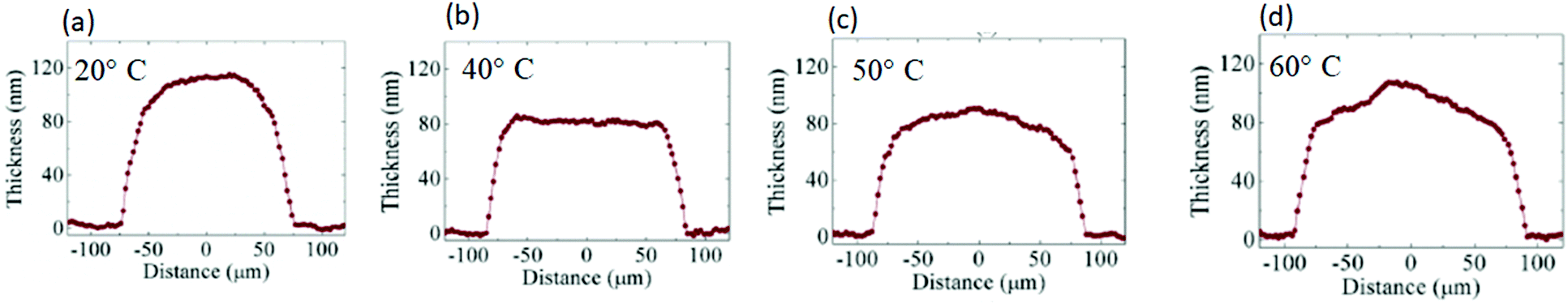 | ||
| Fig. 22 Thickness profile of PEDOT:PSS stripe coated at pre-drying temperatures (a) 20 °C (b) 40 °C (c) 50 °C and (d) 60 °C (reprinted with the permission from ref. 107). | ||
 | ||
| Fig. 23 Picture of 80 OLEDs emitting green light were fabricated with planarized PEDOT:PSS/PVK Layer (reprinted with permission107). | ||
7. Slot-die OLEDs vs. OLEDs made by other R2R solution-based technique
As discussed in the introduction, solution-processable OLEDs can be fabricated using many printing and coating techniques. However, to upscale the fabrication of OLEDs, standardization of R2R coating/printing techniques are crucial. Therefore, it is necessary to compare the quality printed/coated films and performance of OLEDs made with different methods before the standardization of fabrication techniques. Here, we summaries the articles that compare the slot-die OLEDs against other printed/coated OLEDs.Merklein et al.108 studied the comparison of three methods: slot-die coating, inkjet printing, and gravure printing for the fabrication of multi-layer OLEDs. These three techniques were employed to create three films: PEDOT:PSS (HIL), QUPD (cross-linkable HTL), and TSG-M (EML). The quality of films was assessed by measuring thickness and evaluating OLED performance. The tested OLED configuration was: ITO/PEDOT:PSS(HIL)/QUPD(HTL)/TSG-M(EML)/LiF/Al. Noteworthy is that using slot-die coating, all the three materials were able to coat uniformly, but with inkjet just two and with gravure only one. The QUPD layer deposited with an inkjet printer displayed cloud-like formation, which could be due to instability in the drying condition. The PEDOT:PSS and TSG-M printed via the gravure printer show agglomeration and gradient thickness. It is worth pointing out that the ink formulation for slot-die coating was straightforward, whereas, for inkjet and gravure, it involves the addition of co-solvents or additives. Further, investigating the best possible combinations of technique, many OLEDs was fabricated using different methods. The summary of OLEDs performance is shown in Table 3. It turned out that the OLEDs with a slot-die coated PEDOT:PSS and TSG-M, and gravure printed QUPD delivered the best efficiency (13.4 cd A−1). The OLEDs with fully slot-die coated layers performed second best with a current efficiency of 11.8 cd A−1.
| Technique Combination | SS | IS | SG | IG | SI | II |
|---|---|---|---|---|---|---|
| SD: slot-die coating, IJ: inkjet printing, GP: gravure printing. | ||||||
| PEDOT:PSS | SD | IJ | SD | IJ | SD | IJ |
| QUPD | SD | SD | GP | GP | IJ | IJ |
| TSG-M | SD | SD | SD | SD | SD | SD |
| Yield | 9/16 | 13/16 | 10/16 | 11/12 | 6/16 | 11/16 |
| Current effic. (cd A−1) | 10.9 ± 0.9 | 9.7 ± 0.9 | 12.9 ± 0.4 | 8.4 ± 0.8 | 10.6 ± 1.1 | 9.0 ± 0.9 |
| Power effic. (lm W−1) | 2.2 ± 0.1 | 1.7 ± 0.2 | 2.4 ± 0.1 | 1.4 ± 0.1 | 2.0 ± 0.1 | 1.7 ± 0.2 |
| Voltage at 1000 cd m−2 | 11.3 ± 0.8 | 12.0 ± 0.8 | 12.7 ± 0.6 | 13.6 ± 0.4 | 11.3 ± 0.7 | 10.5 ± 0.8 |
Raupp et al.109 compared the thin films and OLEDs manufactured by the two methods: slot-die coating and flexography printing. Their OLED structure was ITO/PEDOT:PSS(HIL)/Green Emitter (EML)/LiF/Al. The PEDOT:PSS was formed via slot-die coating or flexography printing methods, but, the EML was deposited only by slot-die coating. The PEDOT:PSS films deposited via slot-die displayed uniform surface with an average thickness of 31 nm. On the other hand, when deposited by flexography printing, it shows a large thickness variation (0 to 60 nm); the average thickness of the films excluding the edge was 16 nm. Imaging color reflectometry measurements of PEDOT:PSS film coated by both the techniques is shown in Fig. 24. To demonstrate, they fabricated the two kinds of OLEDs, first, with the slot-die coated HTL (slot-die OLEDs) and second with flexography printed HTL (flexography printed OLEDs). On top of the HTL, the emissive layer with an average thickness of 77 nm was formed via slot-die coating. The results show that the current efficiency of slot-die OLEDs (31 cd A−1) was much higher than the flexography OLEDs (11 cd A−1). The high performance of slot-die OLEDs is directly linked to the superior quality of the slot-die coated film. Thus, this study shows the slot-die process has a much higher potential candidate for the fabrication of large-area OLEDs than flexographic printing.
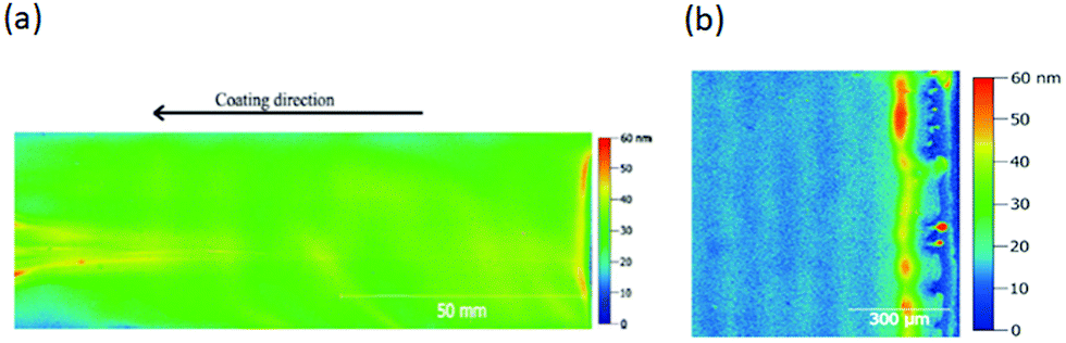 | ||
| Fig. 24 Imaging color reflectometry of PEDOT:PSS films formed by (a) slot-die coating technique and (b) flexography printing technique (reprinted with permission from ref. 109). | ||
Peters et al.110 investigated the formation of an interface between multilayers made from small-molecule. Two kinds of interfaces were examined: one made from slot-die and another from the blade coating technique. The samples were prepared by sequentially depositing the NPB (host for the EML) and BAlq (ETL) on the glass substrate via both methods. The interface of these OLED layers was studied with the help of the XPS (X-ray photoelectron spectroscopy) depth profiling technique. It should be pointed out that the formation of the layer remains the same in both slot-die and blade coating. The XPS results displayed that the sharp interface can be achieved only with the use of orthogonal solvents for coating the two consecutive layers. A mixed layer was found when the non-orthogonal solution was used. For example, Fig. 25 shows the XPS profile of NPB and BAlq bilayer formed via blade coating in which there is a defined interface when BAlq coated from the orthogonal solvent (ethanol) and mixed interface when BAlq coated from non-orthogonal solvent (toluene).
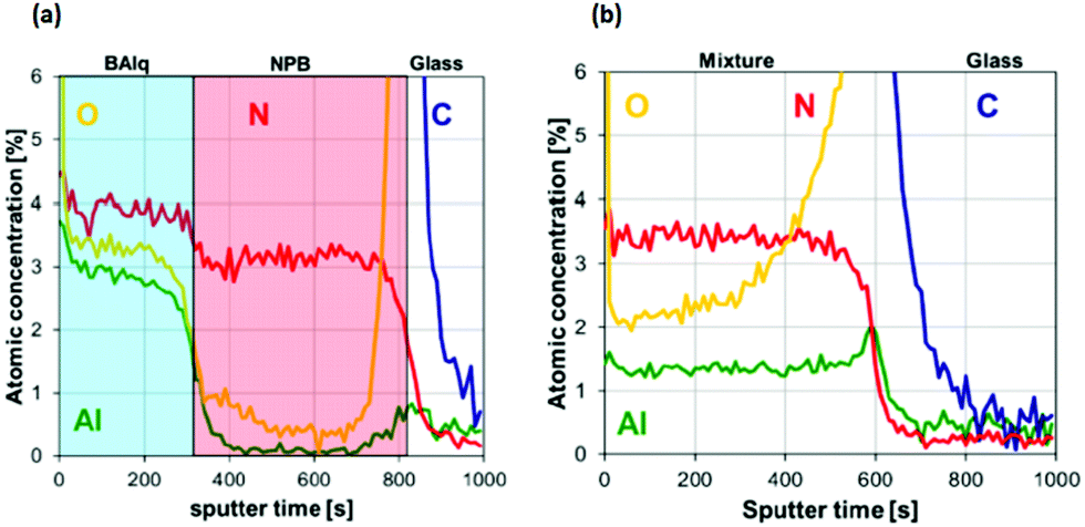 | ||
| Fig. 25 XPS profile of NPB and BAlq bilayer (a) when BAlq coated with orthogonal solvent and (b) when BAlq coated from non-orthogonal solvent (reprinted with permission from ref. 110). | ||
8. Chemical structures of materials
 | ||
| Fig. 26 Chemical structures of materials mentioned in this review article. | ||
9. Conclusions and future outlook
Adoption of solution-based technique to fabricate OLEDs offers many advantages, including low manufacturing cost, large-area coating, and the possibility of using various substrates (glass, plastic, paper, textile, etc.). The slot-die coating method, among many printing and solution coating techniques, has great potential for upscaling OLED production. However, detrimental effects, such as the thickness non-uniformity and dissolution of the underlying layer, responsible for low device efficiency, are inevitable. Substantial advancement has been attained to mitigate such drawbacks by carefully formulating the ink composition and choosing the well-optimized slot-die processing parameters. For coating multi-layer stacks, inks formulated with orthogonal solvents have been widely used to avoid the intermixing of films. Crosslinking approaches, as alternate to orthogonal solvent systems, have also been recently used, but only to a limited extent. In achieving homogeneous films, the slot-die coating parameters such as ink flow rate, coating speed, the substrate to head height, and substrate temperatures are extensively explored. Recent studies show the coating of micro-sized stripes using a double plate (meniscus guide and shim) to eliminate pixel bank structure. The micro stripe coating of PEDOT:PSS, for the fabrication of micro OLEDs was investigated and achieved narrow stripe coating down to 76 μm width. Apart from application in OLEDs, the micro-sized coating can be extended to fabricate other organic devices, including OTFTs, sensors, and memory devices, where micro-patterning is necessary. Solution-processed OLEDs are currently being investigated using various printing and coating techniques. Interestingly, recent evidence shows that the slot-die coated organic films show better quality in comparison to the gravure, inkjet, and flexography printing method; however, more research and development is needed.Most efforts have only focused on the slot-die coating of single or multi-layer of the HIL, HTL, and EML, but only a few present the coating of the ETL/EIL. It is essential to mention that no research work shows the slot-die coating of the metal cathode for a fully slot-die coated OLED. The reported OLEDs are partially slot-die coated because, generally, thermally evaporated aluminum or silver is being used as a cathode. Therefore, it is necessary to stress that there is a need for research to produce the slot-die coated cathode and efficient EIL/ETL. For a multi-layer deposition, usually, non-orthogonal solvents are preferred; however, organic compounds have a similar chemical structure; therefore, it is challenging to find orthogonal solvents. Hence, there are many opportunities to develop crosslinkable materials111,112 and/or solvent switching materials,64 eliminating the need for orthogonal solvents. OLED device performance reproducibility is much-needed information to upscale the OLED production; therefore, we believe it is critical for researchers to study the reproducibility and durability of the devices made via additive manufacturing methods.
Conflicts of interest
There is no conflict of interest.Acknowledgements
All authors would like to thank Alberta Innovates and the Strategic Projects Grant #G2018000901 for financial support.References
- S. J. Zou, Y. Shen, F. M. Xie, J. D. Chen, Y. Q. Li and J. X. Tang, Mater. Chem. Front., 2020, 4, 788–820 RSC.
- Y. Cui, L. Zhou, Y. Jiang, X. Cui, W. Liu, Q. Zhu and H. Zhang, J. Mater. Chem. C, 2020, 8, 5984–5990 RSC.
- M. Koden, OLED Displays and Lighting, 2017, ch. 1 DOI:10.1002/9781119040477.
- S. T. Huo, L. Q. Shao, T. Dong, J. S. Liang, Z. T. Bi, M. He, Z. Li, Z. Gao and J. Y. Song, J. Soc. Inf. Disp., 2020, 28, 36–43 CrossRef.
- K. An, D. G. Yoon and K. T. Kang, Prog. Org. Coat., 2020, 147, 105781 CrossRef CAS.
- Z. Hu, S. Zhang, W. Peng, S. Zhang, Y. Li, D. Li, S. Jiao, S. J. Chen, C. Y. Lee and H. Zhou, Digest of Technical Papers – SID International Symposium, 2019, pp. 1075–1078.
- S. Wang, L. Zhao, B. Zhang, J. Ding, Z. Xie, L. Wang and W.-Y. Wong, iScience, 2018, 6, 128–137 CrossRef CAS.
- D. Han, Y. Khan, K. Gopalan, A. Pierre and A. C. Arias, Adv. Funct. Mater., 2018, 28, 1802986 CrossRef.
- A. Sandström, H. F. Dam, F. C. Krebs and L. Edman, Nat. Commun., 2012, 3, 1002 CrossRef.
- H. Zheng, Y. Zheng, N. Liu, N. Ai, Q. Wang, S. Wu, J. Zhou, D. Hu, S. Yu, S. Han, W. Xu, C. Luo, Y. Meng, Z. Jiang, Y. Chen, D. Li, F. Huang, J. Wang, J. Peng and Y. Cao, Nat. Commun., 2013, 4, 1971 CrossRef.
- L. Zhou, L. Yang, M. J. Yu, Y. Jiang, C. F. Liu, W. Y. Lai and W. Huang, ACS Appl. Mater. Interfaces, 2017, 9, 40533–40540 CrossRef CAS.
- S. Tekoglu, G. Hernandez-Sosa, E. Kluge, U. Lemmer and N. Mechau, Org. Electron., 2013, 14, 3493–3499 CrossRef CAS.
- M. Montanino, G. Sico, C. T. Prontera, A. D. Del Mauro, S. Aprano, M. G. Maglione and C. Minarini, eXPRESS Polym. Lett., 2017, 11, 518–523 CrossRef CAS.
- T. Furukawa, N. Kawamura, J. Inoue, H. Nakada and M. Koden, SID Symposium Digest of Technical Papers, 2015, vol. 46, pp. 1355–1358.
- B. T. Mogg, T. Claypole, D. Deganello and C. Phillips, Transl. Mater. Res., 2016, 3, 015001 CrossRef.
- L. Zhou, M. Yu, X. Chen, S. Nie, W. Y. Lai, W. Su, Z. Cui and W. Huang, Adv. Funct. Mater., 2018, 28, 1705955 CrossRef.
- D. H. Lee, J. S. Choi, H. Chae, C. H. Chung and S. M. Cho, Curr. Appl. Phys., 2009, 9, 161–164 CrossRef.
- B. Park, O. E. Kwon, S. H. Yun, H. G. Jeon and Y. H. Huh, J. Mater. Chem. C, 2014, 2, 8614–8621 RSC.
- L.-S. Yang, H.-F. Meng, Y.-F. Chang, C.-H. Lien, H.-W. Zan, S.-F. Horng, L. Duan, Y. Qiu and C. W. Luo, Org. Electron., 2017, 51, 6–15 CrossRef CAS.
- Y.-F. Chang, H.-F. Meng, G.-L. Fan, K.-T. Wong, H.-W. Zan, H.-W. Lin, H.-L. Huang and S.-F. Horng, Org. Electron., 2016, 29, 99–106 CrossRef CAS.
- G. Koen, S. Jeroen, M. Jean and D. Wim, Proc. SPIE, 2014, 9183 Search PubMed.
- X. Wu, F. Li, W. Wu and T. Guo, Vacuum, 2014, 101, 53–56 CrossRef CAS.
- S. Wang, H. Zhang, B. Zhang, Z. Xie and W.-Y. Wong, Mater. Sci. Eng., R, 2020, 140, 100547 CrossRef.
- Z. Zhan, J. An, Y. Wei, V. T. Tran and H. Du, Nanoscale, 2017, 9, 965–993 RSC.
- D. Han, Y. Khan, J. Ting, S. M. King, N. Yaacobi-Gross, M. J. Humphries, C. J. Newsome and A. C. Arias, Adv. Mater., 2017, 29, 1606206 CrossRef.
- S. Liu, X. Zhang, L. Zhang and W. Xie, Sci. Rep., 2016, 6, 37042 CrossRef CAS.
- K. Gilissen, J. Stryckers, P. Verstappen, J. Drijkoningen, G. H. L. Heintges, L. Lutsen, J. Manca, W. Maes and W. Deferme, Org. Electron., 2015, 20, 31–35 CrossRef CAS.
- K. Albrecht, K. Matsuoka, K. Fujita and K. Yamamoto, Angew. Chem., Int. Ed., 2015, 54, 5677–5682 CrossRef CAS.
- A. Kim, H. Lee, J. Lee, S. M. Cho and H. Chae, J. Nanosci. Nanotechnol., 2011, 11, 546–549 CrossRef CAS.
- D. H. Ahn, S. W. Kim, H. Lee, I. J. Ko, D. Karthik, J. Y. Lee and J. H. Kwon, Nat. Photonics, 2019, 13, 540–546 CrossRef CAS.
- T.-L. Wu, M.-J. Huang, C.-C. Lin, P.-Y. Huang, T.-Y. Chou, R.-W. Chen-Cheng, H.-W. Lin, R.-S. Liu and C.-H. Cheng, Nat. Photonics, 2018, 12, 235–240 CrossRef CAS.
- F. Villani, P. Vacca, G. Nenna, O. Valentino, G. Burrasca, T. Fasolino, C. Minarini and D. della Sala, J. Phys. Chem. C, 2009, 113, 13398–13402 CrossRef CAS.
- Y. J. Kang, R. Bail, C. W. Lee and B. D. Chin, ACS Appl. Mater. Interfaces, 2019, 11, 21784–21794 CrossRef CAS.
- P. Kopola, M. Tuomikoski, R. Suhonen and A. Maaninen, Thin Solid Films, 2009, 517, 5757–5762 CrossRef CAS.
- H. Gorter, M. J. J. Coenen, M. W. L. Slaats, M. Ren, W. Lu, C. J. Kuijpers and W. A. Groen, Thin Solid Films, 2013, 532, 11–15 CrossRef CAS.
- C. Zhong, C. Duan, F. Huang, H. Wu and Y. Cao, Chem. Mater., 2011, 23, 326–340 CrossRef CAS.
- K. An, J. B. Kim, D. G. Yoon, Y. C. Jeong and K. T. Kang, Flexible Printed Electron., 2019, 4, 015009 CrossRef CAS.
- K. An, D. G. Yoon and K.-T. Kang, Prog. Org. Coat., 2020, 147, 105781 CrossRef CAS.
- J.-H. Chang, W.-H. Lin, P.-C. Wang, J.-I. Taur, T.-A. Ku, W.-T. Chen, S.-J. Yan and C.-I. Wu, Sci. Rep., 2015, 5, 9693 CrossRef CAS.
- F. Fei, J. Zhuang, W. Wu, M. Song, D. Zhang, S. Li, W. Su and Z. Cui, RSC Adv., 2015, 5, 608–611 RSC.
- T. J. Faircloth, J. G. Innocenzo and C. D. Lang, SID Symposium Digest of Technical Papers, 2008, vol. 39, pp. 645–647.
- M. Rahmati, S. V. Dayneko, M. Pahlevani and G. C. Welch, ACS Appl. Electron. Mater., 2020, 2, 48–55 CrossRef CAS.
- S. M. Raupp, L. Merklein, S. Hietzschold, M. Zürn, P. Scharfer and W. Schabel, J. Coat. Technol. Res., 2017, 14, 1029–1037 CrossRef CAS.
- L. H. Rossander, H. F. Dam, J. E. Carlé, M. Helgesen, I. Rajkovic, M. Corazza, F. C. Krebs and J. W. Andreasen, Energy Environ. Sci., 2017, 10, 2411–2419 RSC.
- A. Laventure, C. R. Harding, E. Cieplechowicz, Z. Li, J. Wang, Y. Zou and G. C. Welch, ACS Appl. Polym. Mater., 2019, 1, 2168–2176 CrossRef CAS.
- F. Tintori, A. Laventure and G. C. Welch, ACS Appl. Mater. Interfaces, 2019, 11, 39010–39017 CrossRef CAS.
- B. Park, I. G. Bae, O. E. Kwon and H. G. Jeon, RSC Adv., 2016, 6, 101613–101621 RSC.
- G. R. Cagnani, G. Ibáñez-Redín, B. Tirich, D. Gonçalves, D. T. Balogh and O. N. Oliveira, Biosens. Bioelectron., 2020, 165, 112428 CrossRef CAS.
- S. H. Lee and S. Lee, Sensors, 2020, 20, 3748 CrossRef CAS.
- C. Koutsiaki, T. Kaimakamis, A. Zachariadis and S. Logothetidis, Mater. Today: Proc., 2019, 19, 58–64 CAS.
- Z. H. Lin, X. Guo, L. Zhou, C. F. Zhang, J. J. Chang, J. S. Wu and J. Zhang, Org. Electron., 2018, 54, 80–88 CrossRef CAS.
- R. Wang, H.-J. Kwon, X. Tang, H. Ye, C. E. Park, J. Kim, H. Kong and S. H. Kim, Appl. Surf. Sci., 2020, 529, 147198 CrossRef CAS.
- C. W. Tang and S. A. Vanslyke, Appl. Phys. Lett., 1987, 51, 913–915 CrossRef CAS.
- C. W. Tang and S. A. VanSlyke, Appl. Phys. Lett., 1987, 51, 913–915 CrossRef CAS.
- J. H. Burroughes, D. D. C. Bradley, A. R. Brown, R. N. Marks, K. Mackay, R. H. Friend, P. L. Burns and A. B. Holmes, Nature, 1990, 347, 539–541 CrossRef CAS.
- P. K. Bhatnagar, in Nanomaterials and Their Applications, ed. Z. H. Khan, Springer Singapore, Singapore, 2018, pp. 261–287 DOI:10.1007/978-981-10-6214-8_10.
- A. C. Grimsdale, K. Leok Chan, R. E. Martin, P. G. Jokisz and A. B. Holmes, Chem. Rev., 2009, 109, 897–1091 CrossRef CAS.
- P. Data and Y. Takeda, Chem. – Asian J., 2019, 14, 1613–1636 CrossRef CAS.
- M. Poddar and R. Misra, Coord. Chem. Rev., 2020, 421, 213463 CrossRef.
- J. Song, H. Lee, E. G. Jeong, K. C. Choi and S. Yoo, Adv. Mater., 2020, 32, 1907539 CrossRef CAS.
- X. Yang, G. Zhou and W. Y. Wong, Chem. Soc. Rev., 2015, 44, 8484–8575 RSC.
- F. Tintori, A. Laventure, J. Koenig and G. C. Welch, J. Mater. Chem. C, 2020, 8, 13430–13438 RSC.
- D. H. Harris, S. Brixi, B. S. Gelfand, B. H. Lessard and G. C. Welch, J. Mater. Chem. C, 2020, 8, 9811–9815 RSC.
- C. R. Harding, J. Cann, A. Laventure, M. Sadeghianlemraski, M. Abd-Ellah, K. R. Rao, B. S. Gelfand, H. Aziz, L. Kaake, C. Risko and G. C. Welch, Mater. Horiz., 2020, 7, 2959–2969 RSC.
- B. V. Khau, L. R. Savagian, M. De Keersmaecker, M. A. Gonzalez and E. Reichmanis, ACS Mater. Lett., 2019, 1, 599–605 CrossRef CAS.
- B. Schmatz, Z. Yuan, A. W. Lang, J. L. Hernandez, E. Reichmanis and J. R. Reynolds, ACS Cent. Sci., 2017, 3, 961–967 CrossRef CAS.
- D. Ho, J. Lee, S. Park, Y. Park, K. Cho, F. Campana, D. Lanari, A. Facchetti, S. Seo, C. Kim, A. Marrocchi and L. Vaccaro, J. Mater. Chem. C, 2020, 8, 5786–5794 RSC.
- S. Zhang, L. Ye, H. Zhang and J. Hou, Mater. Today, 2016, 19, 533–543 CrossRef CAS.
- D. Prat, A. Wells, J. Hayler, H. Sneddon, C. R. McElroy, S. Abou-Shehada and P. J. Dunn, Green Chem., 2016, 18, 288–296 RSC.
- N. T. Kalyani, H. Swart and S. J. Dhoble, in Principles and Applications of Organic Light Emitting Diodes (OLEDs), ed. N. T. Kalyani, H. Swart and S. J. Dhoble, Woodhead Publishing, 2017, pp. 227–252 DOI:10.1016/B978-0-08-101213-0.00009-6.
- P.-A. Will and S. Reineke, in Handbook of Organic Materials for Electronic and Photonic Devices, ed. O. Ostroverkhova, Woodhead Publishing, 2nd edn, 2019, pp. 695–726 DOI:10.1016/B978-0-08-102284-9.00021-8.
- N. C. Erickson and R. J. Holmes, Adv. Funct. Mater., 2014, 24, 6074–6080 CrossRef CAS.
- Z. Yang, Z. Mao, Z. Xie, Y. Zhang, S. Liu, J. Zhao, J. Xu, Z. Chi and M. P. Aldred, Chem. Soc. Rev., 2017, 46, 915–1016 RSC.
- T.-Y. Li, J. Wu, Z.-G. Wu, Y.-X. Zheng, J.-L. Zuo and Y. Pan, Coord. Chem. Rev., 2018, 374, 55–92 CrossRef CAS.
- Y. Sun and S. R. Forrest, Nat. Photonics, 2008, 2, 483–487 CrossRef CAS.
- L. F. R. Pereira, Organic Light Emitting Diodes: The Use of Rare Earth and Transition Metals, Pan Stanford, 2012 Search PubMed.
- T. E. Umbach, S. Röllgen, S. Schneider, H. Klesper, A. M. Umbach and K. Meerholz, Adv. Eng. Mater., 2020, 22, 1900897 CrossRef CAS.
- S. Reineke, M. Thomschke, B. Lüssem and K. Leo, Rev. Mod. Phys., 2013, 85, 1245–1293 CrossRef CAS.
- D. D. S. Pereira, P. Data and A. P. Monkman, Display and Imaging, 2017, 2, 323–337 Search PubMed.
- C. Ware, in Information Visualization, ed. C. Ware, Morgan Kaufmann, Boston, 3rd edn, 2013, pp. 95–138 DOI:10.1016/B978-0-12-381464-7.00004-1.
- Spectral color, (accessed In Wikipedia. Retrieved from https://en.wikipedia.org/wiki/Spectral_color).
- J. Lin, Printed Electronics, 2016, ch. 4, pp. 106–144 DOI:10.1002/9781118920954.
- R. R. Søndergaard, M. Hösel and F. C. Krebs, J. Polym. Sci., Part B: Polym. Phys., 2013, 51, 16–34 CrossRef.
- B. Roth, R. R. Søndergaard and F. C. Krebs, Handbook of Flexible Organic Electronics: Materials, Manufacturing and Applications, 2014, pp. 171–197 DOI:10.1016/B978-1-78242-035-4.00007-5.
- X. Ding, J. Liu and T. A. L. Harris, AIChE J., 2016, 62, 2508–2524 CrossRef CAS.
- J. B. Whitaker, D. H. Kim, B. W. Larson, F. Zhang, J. J. Berry, M. F. A. M. van Hest and K. Zhu, Sustainable Energy Fuels, 2018, 2, 2442–2449 RSC.
- Y. R. Chang, H. M. Chang, C. F. Lin, T. J. Liu and P. Y. Wu, J. Colloid Interface Sci., 2007, 308, 222–230 CrossRef CAS.
- Y. R. Chang, C. F. Lin and T. J. Liu, Polym. Eng. Sci., 2009, 49, 1158–1167 CrossRef CAS.
- K.-J. Choi, J.-Y. Lee, D.-K. Shin and J. Park, J. Phys. Chem. Solids, 2016, 95, 119–128 CrossRef CAS.
- A. C. M. Colella, J. Griffin, J. Kingsley, N. Scarratt, B. Luszczynska and J. Ulanski, Micromachines, 2019, 10, 53 CrossRef.
- S. V. Dayneko, M. Rahmati, M. Pahlevani and G. C. Welch, J. Mater. Chem. C, 2020, 8, 2314–2319 RSC.
- R. Abbel, I. de Vries, A. Langen, G. Kirchner, H. t’Mannetje, H. Gorter, J. Wilson and P. Groen, J. Mater. Res., 2017, 32, 2219–2229 CrossRef CAS.
- S. M. Raupp, L. Merklein, M. Pathak, P. Scharfer and W. Schabel, Chem. Eng. Sci., 2017, 160, 113–120 CrossRef CAS.
- K.-J. Choi, J.-Y. Lee, J. Park and Y.-S. Seo, Org. Electron., 2015, 26, 66–74 CrossRef CAS.
- L. Merklein, M. Mink, D. Kourkoulos, B. Ulber, S. M. Raupp, K. Meerholz, P. Scharfer and W. Schabel, J. Coat. Technol. Res., 2019, 16, 1643–1652 CrossRef CAS.
- K. K. Sears, M. Fievez, M. Gao, H. C. Weerasinghe, C. D. Easton and D. Vak, Sol. RRL, 2017, 1, 1700059 CrossRef.
- B.-Y. Wang, E.-S. Lee, D.-S. Lim, H. W. Kang and Y.-J. Oh, RSC Adv., 2017, 7, 7540–7546 RSC.
- H. Lee, D. Lee, J. Hwang, D. Nam, C. Byeon, S. H. Ko and S. Lee, Opt. Express, 2014, 22, 8919–8927 CrossRef.
- M. Cann, M. J. Large, S. J. Henley, D. Milne, T. Sato, H. Chan, I. Jurewicz and A. B. Dalton, Mater. Today Commun., 2016, 7, 42–50 CrossRef CAS.
- H. Jeong, S. Park, J. Lee, P. Won, S.-H. Ko and D. Lee, Adv. Electron. Mater., 2018, 4, 1800243 CrossRef.
- S. Mühl, M. Klein, M. Törker and A. Richter, SID Symposium Digest of Technical Papers, 2015, vol. 46, pp. 1664–1667.
- D. Shin, J.-Y. Lee, K.-Y. Hong, J. Park and Y.-S. Seo, Thin Solid Films, 2016, 619, 179–186 CrossRef CAS.
- D. Shin, J. Lee, G. Kim and J. Park, IEEE Trans. Electron Devices, 2018, 65, 4506–4512 CAS.
- G. Kim, J. Lee, D. Shin and J. Park, IEEE Trans. Electron Devices, 2019, 66, 1041–1049 CAS.
- J. Lee, X. Li and J. Park, IEEE Trans. Electron Devices, 2019, 66, 5221–5229 CAS.
- G.-E. Kim, D.-K. Shin, J.-Y. Lee and J. Park, Org. Electron., 2019, 66, 116–125 CrossRef CAS.
- J. Lee and J. Park, Thin Solid Films, 2020, 693, 137672 CrossRef CAS.
- L. Merklein, D. Daume, F. Braig, S. Schlisske, T. Rödlmeier, M. Mink, D. Kourkoulos, B. Ulber, M. Di Biase, K. Meerholz, G. Hernandez-Sosa, U. Lemmer, H. M. Sauer, E. Dörsam, P. Scharfer and W. Schabel, Colloids Interfaces, 2019, 3, 32 CrossRef CAS.
- S. Raupp, D. Daume, S. Tekoglu, L. Merklein, U. Lemmer, G. Hernandez-Sosa, H. M. Sauer, E. Dörsam, P. Scharfer and W. Schabel, Adv. Mater. Technol., 2017, 2, 1600230 CrossRef.
- K. Peters, S. Raupp, H. Hummel, M. Bruns, P. Scharfer and W. Schabel, AIP Adv., 2016, 6, 065108 CrossRef.
- S. V. Kunz, C. M. Cole, A. Welle, P. E. Shaw, P. Sonar, N.-P. Thoebes, T. Baumann, S. D. Yambem, E. Blasco, J. P. Blinco and C. Barner-Kowollik, Macromolecules, 2019, 52, 9105–9113 CrossRef CAS.
- W. Sun, Y. Deng, Y. Jin, X. Guo and Q. Zhang, ACS Appl. Polym. Mater., 2020, 2, 3274–3281 CrossRef CAS.
| This journal is © The Royal Society of Chemistry 2021 |