
 Open Access Article
 This Open Access Article is licensed under a
 Creative Commons Attribution 3.0 Unported Licence
All-inorganic CsPbBr3 perovskite: a promising choice for photovoltaics
Saad
Ullah
 ,
Jiaming
Wang
,
Peixin
Yang
,
Linlin
Liu
,
Shi-E.
Yang
,
Tianyu
Xia
,
Haizhong
Guo
* and
Yongsheng
Chen
*
,
Jiaming
Wang
,
Peixin
Yang
,
Linlin
Liu
,
Shi-E.
Yang
,
Tianyu
Xia
,
Haizhong
Guo
* and
Yongsheng
Chen
*
Key Laboratory of Materials Physics of Ministry of Education, School of Physics and Microelectronics, Zhengzhou University, Zhengzhou 450052, China. E-mail: hguo@zzu.edu.cn; chysh2003@zzu.edu.cn
First published on 9th December 2020
Abstract
In recent years, inorganic CsPbBr3-based perovskites have accomplished considerable progress owing to their superior stability under harsh humid environment. The power conversion efficiency (PCE) of CsPbBr3 perovskite solar cells (PSCs) has seen an unprecedented development from 5.74% to 10.91% with the improvement of the CsPbBr3 crystal quality. Despite extensive research efforts, the device efficiency of the CsPbBr3-based PSCs still lags behind that of other hybrid perovskite materials. Therefore, there is a significant interest in further boosting the performance of all-inorganic CsPbBr3 PSCs by the synergic optimization of films and device interfaces. In this review, we have discussed and summarized recent advances and methodologies related to CsPbBr3 films and PSCs. Furthermore, we discuss different fabrication strategies such as solution-based and vapor-based methods and their influence on the properties of CsPbBr3, particularly the morphology of films. Moreover, the timeline of improvement of the device efficiency from 2015 to 2020 is comprehensively addressed and developments are clearly sorted out by addressing critical factors influencing the photovoltaic performance. We further highlight state-of-the-art engineering strategies for CsPbBr3 PSCs that facilitate the crystallization control, charge extraction, suppression of charge recombination, and defect passivation in a systematic manner. At the end of the review, the summary and perspectives are presented along with beneficial guidelines for developing highly efficient and stable CsPbBr3 PSCs.
 Saad Ullah | Saad Ullah is currently a doctoral research fellow at the School of Physics and Microelectronics, Zhengzhou University. He obtained his bachelor's degree from the International Islamic University in 2015 and his master's degree from the Air University, Pakistan in 2018. His current research focuses on perovskite solar cells. |
 Jiaming Wang | Jiaming Wang is a graduate student at the School of Physics and Microelectronics, Zhengzhou University. She obtained her undergraduate degree from Luliang University in 2018. Her current research focuses on inorganic-perovskite solar cells. |
 Haizhong Guo | Haizhong Guo is currently a professor of physics at the Key Laboratory of Material Physics of Ministry of Education, School of Physics and Microelectronics, Zhengzhou University. Prof. Guo received his PhD degree in condensed matter physics from the Institute of Physics, CAS in 2005. From 2005 to 2009, he worked as a postdoc at the University of Alabama, University of California at Davis, and Louisiana State University. Then, he was an associate professor at the Institute of Physics, CAS from 2009 to 2017. He joined Zhengzhou University as a professor in 2017. His research focuses on the novel physical phenomena emerging in low-dimension transition-metal oxide heterostructures. |
 Yongsheng Chen | Yongsheng Chen is currently an associate professor at the School of Physics and Microelectronics, Zhengzhou University. He obtained his PhD degree from Hefei Institutes of Physical Science, Chinese Academy of Sciences in 2010. His current research focuses on perovskite solar cells. |
1. Introduction
Solar energy released by solar radiation accounts for almost 99% of the energy produced on Earth. However, the global warming and over-reliance of humans on fossil fuels pose a threat of climate change. Therefore, there is a desperate need to address this possible threat by harvesting clean energy using energy conversion devices. Photovoltaics are an expedient and sustainable method that can deliver inexhaustible clean solar energy to mankind with a low cost of electricity. Since the development of first solar panel in 1954 by Bell laboratories, the conversion of solar energy has always been a hot topic among researchers.1 To date, silicon solar cells have been at the commercial forefront of the photovoltaic industry.2 However, the fabrication of silicon solar cells is considered to be expensive owing to the high melting point of silicon, which limits their long-term potential. In last few years, organic–inorganic hybrid perovskite solar cells have attracted considerable attention in the photovoltaic community owing to their high efficiency, cost-effective fabrication, low exciton binding energies, balanced carrier mobility, high absorption coefficients, long carrier diffusion lengths, and suitable energy bandgaps.3–7 The extraordinary development has seen an increase in PCE from 3.8% to the state-of-art values of 25.2%.8–17 To commercialize perovskite solar cells, their large-scale fabrication, improvement in the stability and efficiency, and efficient reproducibility is crucial. However, organic–inorganic hybrid PSCs suffer from compositional degradation under heat and moisture mainly due to the high volatility of organic cations.18–20 Organic cations such as MA+ and FA+ are expected to react with water molecules or under the ambient thermal environment to form hydrates, which cause instability and the degradation of the device.21–26 The instability of organic cation-based PSCs is a critical flaw that impedes the commercialization of PSCs. Recent studies have suggested that the environmental tolerance of PSCs can be improved by the introduction of inorganic cations such as (Cs+) instead of organic (MA+, FA+) ions.27,28 To enhance the efficiency of PSCs, many methods such as solvent engineering, interfacial engineering, and bandgap engineering have been developed. Generally, there are three main types of halides, namely, CsPbI3, CsPbBr3, and CsPbCl3.29–32 The intrinsic tolerance to defects is one of the exceptional qualities of these halide perovskites as the defect states exist within the valence and conduction bands of these materials. In last few years, significant research attention has been given to improve the device efficiency of inorganic halide perovskites. Fig. 1 shows the comparison between the theoretically-predicted (Shockley–Queisser limit) and experimentally-attained PCEs of inorganic halide perovskites. Among all exploited halide perovskites, CsPbI3 is the most studied perovskite due to its optimal bandgap of 1.73 eV and high efficiency >19%. However, the desired perovskite phase of CsPbI3 is only stable at higher temperatures (>300) and the material experiences an undesirable phase transition to the non-perovskite phase under ambient conditions.33,34 This undesirable phase transition, followed by the presence of moisture, hinders the potential of CsPbI3 as an efficient solar cell device. Although, CsPbCl3 is stable at the room temperature, due to its high bandgap of 3.0 eV, it is undesirable for solar cell applications. CsPbBr3 also possesses a larger bandgap of 2.3 eV but demonstrates appropriate light harvesting characteristics and superior stability in ambient conditions. CsPbBr3 halide single-crystals have demonstrated ultra-high electron mobility of 1000 cm2 V s−1 and an electron lifetime of 2.5 μs, which is relatively higher than that of full cesium-based perovskites.35–38 Based on these characteristics, one may further envisage the potential of CsPbr3 as a promising material for photovoltaic applications. | ||
| Fig. 1 Comparison between the theoretically- and experimentally-attained PCEs of inorganic halide perovskites. | ||
In this review, we have summarized the challenges and strategies for the purposes of performance enhancement and commercialization of CsPbBr3 PSCs. The viewpoints of stability issues related with CsPbBr3 PSCs and the comparison with the other PSCs is systematically addressed, followed by the discussion on different fabrication approaches for designing high-quality films and their role in improving the photovoltaic performance of CsPbBr3 PSCs. The importance of the fundamental configuration of a perovskite photo-absorption layer, transport layers (ETL, HTL), and the “golden triangle” criteria for carbon-based CsPbBr3 PSCs is reviewed. Furthermore, we have comprehensively analyzed the potential engineering strategies including compositional engineering, additive engineering, and interfacial engineering. At the end of the review, discussions on the possible solutions to the developmental bottlenecks are suggested to provide beneficial guidance for improving the device efficiency of CsPbBr3 PSCs.
2. Crystal structure and properties of CsPbBr3
The CsPbBr3 perovskite has a similar structure to the mineral CaTiO3 and is designated by the chemical formula ABX3 (X = I, Br, and Cl). In general, CsPbBr3 possesses an octahedron structure in which Pb2+ and Br− forms a 3D network of corner-sharing [PbBr6]4− octahedra with Cs+ ions occupying the octahedral voids (Fig. 2a). The structural tenability of the ABX3 perovskite is limited due to the presence of rigid structural constraints. The phase stability and distortion of the CsPbBr3 structure is predicted by the Goldschmidt tolerance factor (τ), which is given as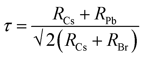 | (1) |
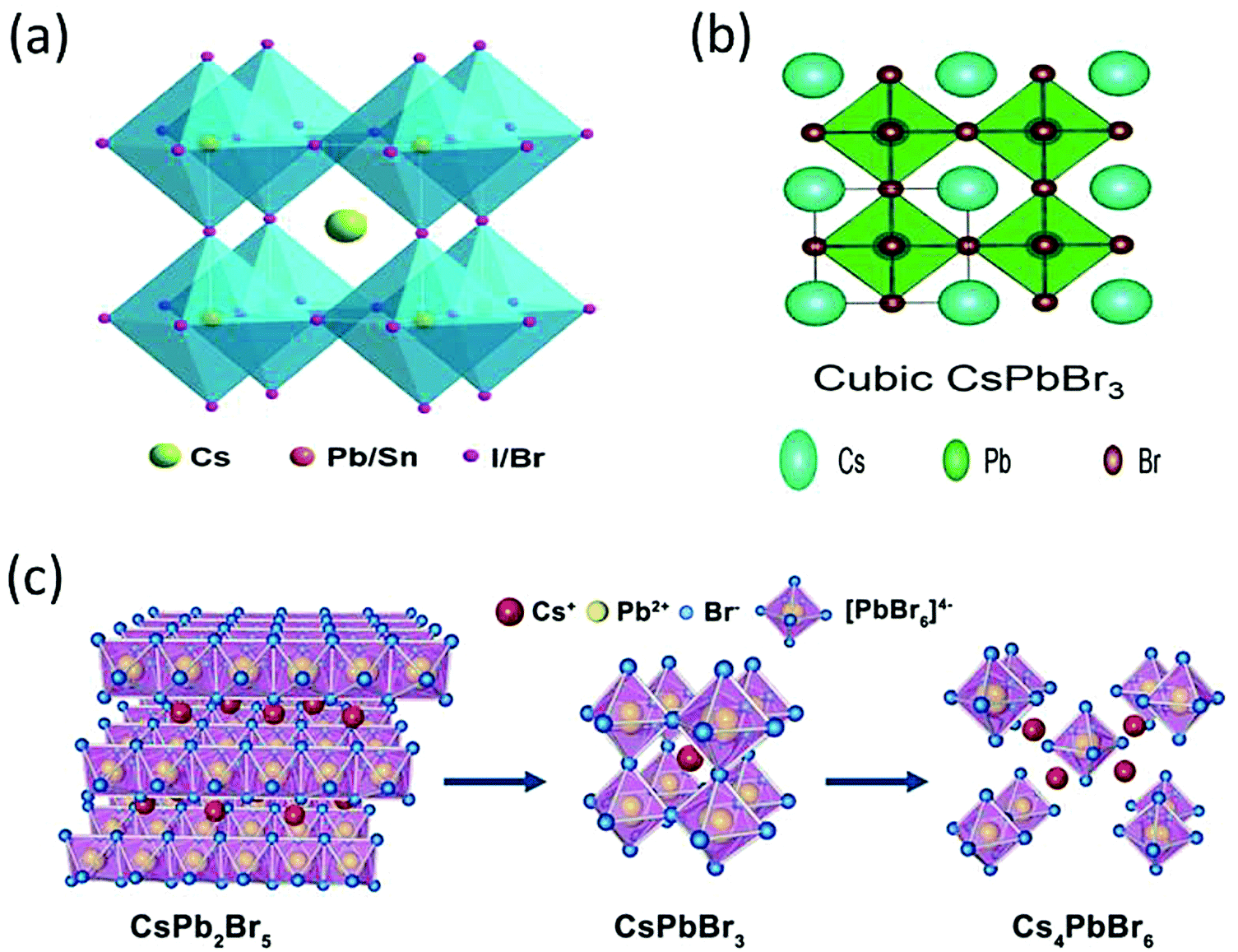 | ||
| Fig. 2 (a) The crystal structure of an inorganic CsPbX3 (X = I, Br, Cl) perovskite. Reprinted with permission ref. 83. (b) Cubic structure of CsPbBr3. Reprinted with permission ref. 84. Copyright 2019, The Royal Society of Chemistry. (c) Three-dimensional crystal structure models of CsPb2Br5, CsPbBr3, and Cs4PbBr6 structures. Reprinted with permission ref. 120. Copyright 2019, American Chemical Society. | ||
CsPbBr3 possesses two derivative phases, i.e., CsPb2Br5 and Cs4PbBr6, as shown in Fig. 2c. The former exhibits a two-dimensional layer structure in which Cs+ ions are interposed between the two layers of Pb–Br coordinated polyhedrons. The latter shows a 0-D structure based on the [PbBr]4− octahedra, which are disconnected from each other by CsBr bridges due to abundant CsBr.48–54 The formation mechanism of both the phases is shown in the following equations.
| CsBr + PbBr2 → CsPbBr3 | (2) |
| CsBr + 2PbBr2 → CsPbBr5 | (3) |
| 4CsBr + PbBr2 → Cs4PbBr6 | (4) |
CsPbBr3 possesses various morphologies such as nanocrystals, single crystals, and bulk films. CsPbBr3 nanocrystals exhibit a maximum photoluminescence quantum yield (PLQY) of 95%, while the other halide perovskites such as CsPbI3 and CsPbCl3 exhibit lower PLQY of 70% and 10%, respectively.59 CsPbBr3 perovskite is intended to detect wide-band absorption of 270–532 nm, which is important for increasing the power output of PSCs. The carrier diffusion length of 80 nm was first reported for the CsPbBr3 films, while an electron mobility of 1000 cm2 V−1 s−1 and electron lifetime of 2.5 ms were realized for the CsPbBr3 single-crystals.60,61 For single crystals of CsPbBr3, the electron and hole diffusion lengths were reported as 1 μm and 12 μm, respectively.62 High diffusion lengths, wide-band absorption, and high carrier mobility make CsPbBr3 a promising material for achieving high PCE and photocurrent density. Owing to the high bandgap of 2.3 eV,63–66 CsPbBr3 PSC exhibits high open-circuit voltage (Voc) exceeding 1.6 V,67,68 which can also be accredited to the diminishing of the film defects with the precise control of crystal growth.
3. Stability of CsPbBr3
The stability of the halide perovskites is greatly affected by the external environmental conditions, such as heat, water, light illumination, and air (Fig. 3a). Compared with the other organic–inorganic halide perovskites, CsPbBr3 shows superior moisture, light, and thermal stability under ambient environments. In this section, we will discuss the highly stable nature of CsPbBr3 in comparison with other organic–inorganic halide PSCs.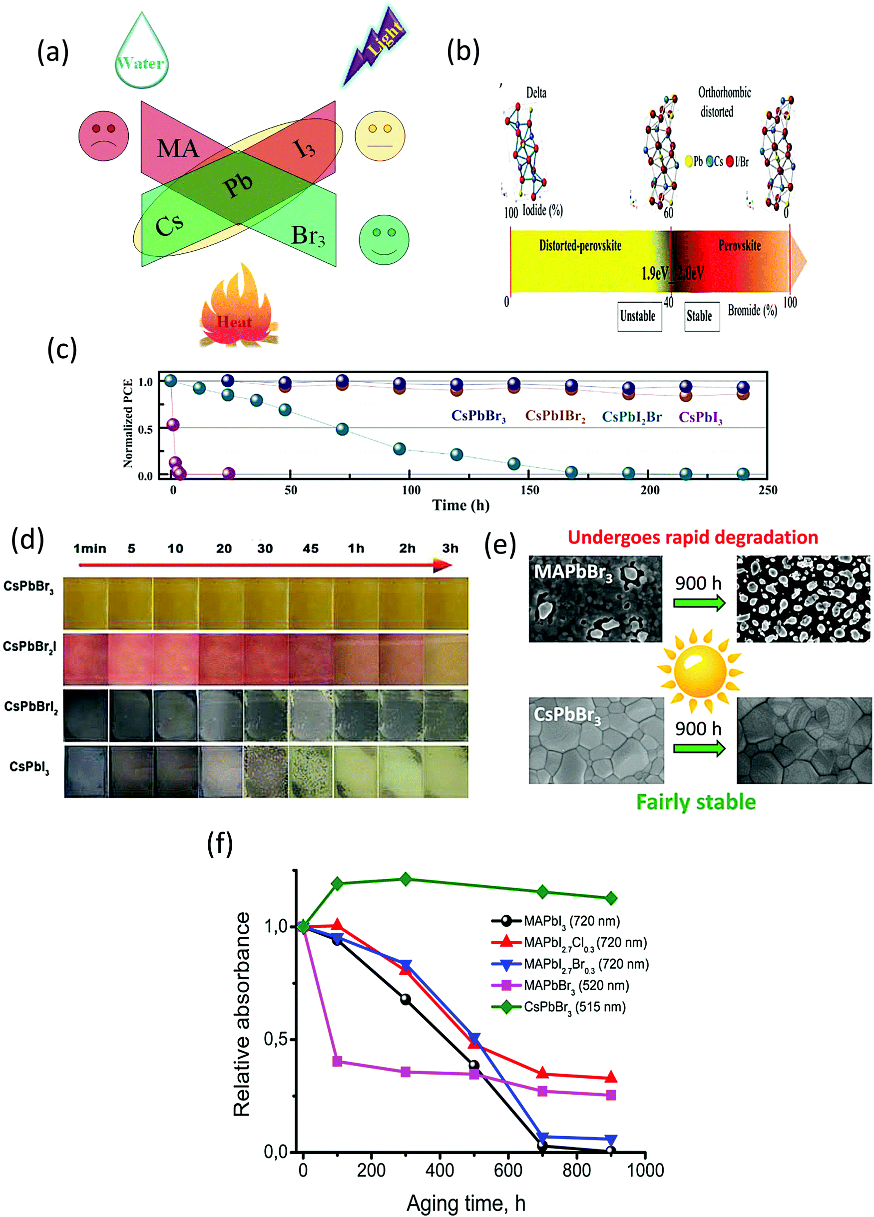 | ||
| Fig. 3 (a) Impact of the surrounding conditions on the stability of the perovskites. (b) Illustrating the crystal structure of the perovskites as a function of the I/Br ratio. Reprinted with permission ref. 80. Copyright 2018, Wiley-VCH. (c) The EQE spectra of the corresponding PSC devices. Reprinted with permission ref. 81. (d) The color evolution of CsPbI3−xBrx films exposed to ambient environment(25 °C, 40% RH). Reprinted with permission ref. 82. Copyright 2019, Royal Society of Chemistry. (e) A comparison of the photo-stability of CsPbBr3 and MAPbBr3 perovskites. (f) The photochemical stability of various halide perovskites monitored by the progression of their absorption spectra under illumination. Reprinted with permission ref. 249. Copyright 2017, American Chemical Society. | ||
3.1 Stability comparison between the hybrid and all-inorganic perovskites
The stability issue of the organic–inorganic hybrid perovskites appears to be the bottleneck that hinders their industrialization. Although MAPbI3 and CsPbI3 are highly efficient materials, their low stability in ambient conditions has been noticed since the early stage of research on perovskite materials. Controlling the interplay between the bandgap and phase stability of inorganic PSCs is a challenging task for researchers. The larger ionic radii of I− as compared to that of Br− affects the phase stability and restricts the processing fabrication of devices under the ambient environment. By enhancing the Br content, the phase stability can be improved significantly. Abate's group80 examined the phase stability of CsPbX3 perovskites and found out that a clear boundary situated at the I/Br ratio of 3![[thin space (1/6-em)]](https://www.rsc.org/images/entities/char_2009.gif) :2 separates the stable and distorted perovskite lattices (Fig. 3b). Although the materials (Eg < 2.0 eV) offer an ideal bandgap for highly efficient devices but due to their unstable nature, their photovoltaic performance is restricted. The photovoltaic performance evolution of the perovskite nanocomposites with respect to time was further investigated by Jiang and coworkers.81 They found that all the iodide-rich nanocomposites were unstable and suffer from unfavorable phase transition, while the CsPbBr3 perovskite exhibited a superior device, as shown in Fig. 3c. Also, the other inorganic counterparts of CsPbBr3 such as CsPbI3, CsPbI2Br, and CsPbIBr2 degrade rapidly under ambient conditions, as suggested in Fig. 3d. However, CsPbBr3 shows superior stability in ambient conditions without any changes in its color and shape,82 and thus can be utilized as a promising light harvesting material. Halide perovskites suffer from photo-induced degradation, which affects their long-term stability.245,246 However, limited research has been done on the exploration of the origins of this photoinduced degradation. It has been reported that Cs-based materials exhibit superior light stabilities compared to MA-based materials. Previously, Hodes group247 studied the impact of electron beam irradiation and light on different halide perovskites. Their findings highlighted that the CsPbBr3-based cells showed no prominent signs of degradation when exposed to the electron beam, while the MAPbBr3-based cells showed a rapid decay and dramatic change in the morphology from crystalline to amorphous films. Zhou et al.248 reported that the Cs-based perovskite solar cells can maintain >99% of their initial efficiency (10.3%) under AM1.5G illumination after 1500 h, while the MA-based devices were harshly degraded after 50 h of tracking operation. Furthermore, comprehensive research on the photochemical stability of halide perovskites was made by the Akbulatov's group.249 From their reported work, it can be inferred that CsPbBr3 exhibits a higher degree of photostability without any prominent degradation as compared with MAPbBr3 (Fig. 3e). After continuous illumination, the CsPbBr3 absorption bands surprisingly revealed an increase in the intensity, which was further supported by the morphological investigations, indicating no significant variation in the composition of the CsPbBr3 perovskite films. A comparison of the photostability of different halide perovskites is depicted in Fig. 3f, which also clearly indicates that CsPbBr3 exhibits superior stability compared to its counterparts. The origins of photo-stability in the CsPbBr3 QDs were addressed in the study made by Chen et al.250 They found out that the presence of non-radiative recombination was indicated in the PL QY spectra of the degraded samples, while PL decays indicate the presence of trap site emission in CsPbBr3, which was prominent in the PL decays. The aggregation of CsPbBr3 QDs and elimination of the capping agent will produce several surface/interface dangling bonds, which can act as emissive and non-emissive trap states. It was further proposed that the photo-stability of CsPbBr3 can be improved with surface passivation strategies using polymer layers or tightly bonded agents.
:2 separates the stable and distorted perovskite lattices (Fig. 3b). Although the materials (Eg < 2.0 eV) offer an ideal bandgap for highly efficient devices but due to their unstable nature, their photovoltaic performance is restricted. The photovoltaic performance evolution of the perovskite nanocomposites with respect to time was further investigated by Jiang and coworkers.81 They found that all the iodide-rich nanocomposites were unstable and suffer from unfavorable phase transition, while the CsPbBr3 perovskite exhibited a superior device, as shown in Fig. 3c. Also, the other inorganic counterparts of CsPbBr3 such as CsPbI3, CsPbI2Br, and CsPbIBr2 degrade rapidly under ambient conditions, as suggested in Fig. 3d. However, CsPbBr3 shows superior stability in ambient conditions without any changes in its color and shape,82 and thus can be utilized as a promising light harvesting material. Halide perovskites suffer from photo-induced degradation, which affects their long-term stability.245,246 However, limited research has been done on the exploration of the origins of this photoinduced degradation. It has been reported that Cs-based materials exhibit superior light stabilities compared to MA-based materials. Previously, Hodes group247 studied the impact of electron beam irradiation and light on different halide perovskites. Their findings highlighted that the CsPbBr3-based cells showed no prominent signs of degradation when exposed to the electron beam, while the MAPbBr3-based cells showed a rapid decay and dramatic change in the morphology from crystalline to amorphous films. Zhou et al.248 reported that the Cs-based perovskite solar cells can maintain >99% of their initial efficiency (10.3%) under AM1.5G illumination after 1500 h, while the MA-based devices were harshly degraded after 50 h of tracking operation. Furthermore, comprehensive research on the photochemical stability of halide perovskites was made by the Akbulatov's group.249 From their reported work, it can be inferred that CsPbBr3 exhibits a higher degree of photostability without any prominent degradation as compared with MAPbBr3 (Fig. 3e). After continuous illumination, the CsPbBr3 absorption bands surprisingly revealed an increase in the intensity, which was further supported by the morphological investigations, indicating no significant variation in the composition of the CsPbBr3 perovskite films. A comparison of the photostability of different halide perovskites is depicted in Fig. 3f, which also clearly indicates that CsPbBr3 exhibits superior stability compared to its counterparts. The origins of photo-stability in the CsPbBr3 QDs were addressed in the study made by Chen et al.250 They found out that the presence of non-radiative recombination was indicated in the PL QY spectra of the degraded samples, while PL decays indicate the presence of trap site emission in CsPbBr3, which was prominent in the PL decays. The aggregation of CsPbBr3 QDs and elimination of the capping agent will produce several surface/interface dangling bonds, which can act as emissive and non-emissive trap states. It was further proposed that the photo-stability of CsPbBr3 can be improved with surface passivation strategies using polymer layers or tightly bonded agents.
In the pioneer report on CsPbBr3 PSCs, it was demonstrated that CsPbBr3 can work equally well as MAPbBr3, showcasing high open circuit voltage. What was more interesting about CsPbBr3 was its superior stability compared with MAPbBr3.86,87 Under an illumination period of 5 h, CsPbBr3 exhibited a photocurrent density decay of just 13% from the maximum value, in contrast to MAPbBr3, which showed a faster decay of 55%. When aging tests were performed in relative humidity in the range of 60–70%, CsPbBr3 showed no significant decay in the efficiency for 2 weeks while MAPbBr3 suffered heavy efficiency loss of about 83%. Furthermore, the thermal stability comparison of CsPbBr3 and MAPbI3 revealed that inorganic CsPbBr3 can show excellent thermal stability up to 580 °C, while MAPbI3 started to lose mass at 200 °C (Fig. 4a). The firstly prepared carbon-based CsPbBr3 perovskite films32 were one of the most stable PSC to date, showing no signs of degradation under high-humidity conditions for about 720 h (RH 90–95%, 100 °C) and 3 months (RH 90–95%, 25 °C) (Fig. 4b and c). The higher thermal stability of the carbon-based CsPbBr3 is due to the absence of metal contacts (Ag and Au) inward diffusion. Nagabhushana et al.88 also reported the thermodynamically unstable nature of MAPbI3, making it vulnerable to decomposition under ambient conditions. Furthermore, Zhou et al.89 tested the stability of the CsPbBr3 thin films stored in ambient conditions (T = 298 K, 40% humidity). The UV absorption spectra showed no prominent change in the absorption after nearly 2000 h of storage, which is due to the stable nature of CsPbBr3 (Fig. 4d). Furthermore, the thermal stabilities of the CsPbBr3 and MAPbI3 PSCs using MnS as an HTL were also compared.120 After 100 days of harsh humidity exposure (80% RH, 85 °C), CsPbBr3 yet again proved to be more moisture tolerant than MAPbI3 as it retained 80% of its initial PCE, as depicted in Fig. 4e and f. However, the referenced devices showed poor stability without MnS HTL, which shows that HTL has a strong influence in improving the stability of CsPbBr3. This also shows the importance of inorganic HTL over organic HTL in improving the device stability in ambient conditions.
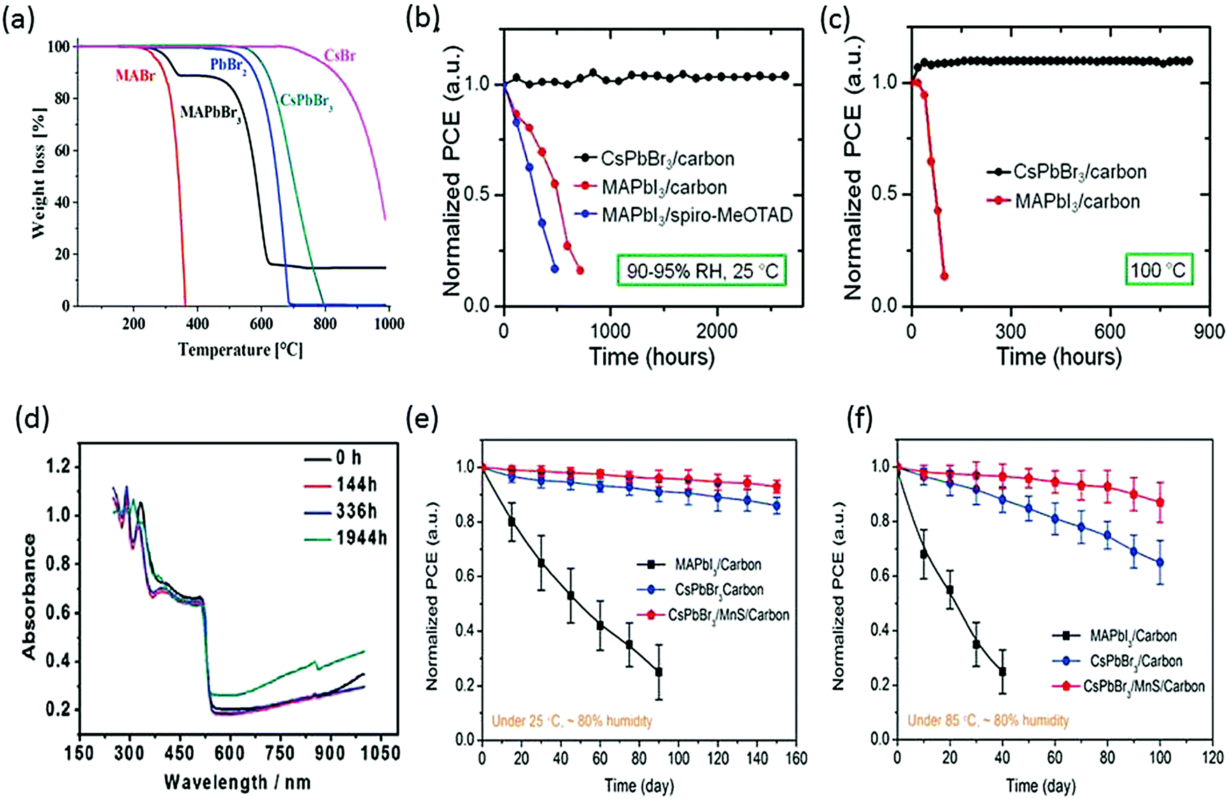 | ||
| Fig. 4 (a) Thermogravimetric analyses of MAPbBr3 and CsPbBr3 perovskites. Reprinted with permission ref. 86. Copyright 2019, American Chemical Society. (b) Normalized device efficiencies of CsPbBr3/carbon-based device, MAPbI3/carbon- and MAPbI3/spiro-MeOTAD-based devices in relative humidity of 90–95% at 25 °C. (c) Normalized device efficiencies as a function of time for CsPbBr3/carbon-based devices and MAPbI3/carbon-based devices heated at 100 °C temperature (90–95% RH). Reprinted with permission ref. 32. Copyright 2016, American Chemical Society. (d) UV-vis absorbance spectra of the CsPbBr3 films stored in ambient conditions in air (40% RH, T = 298 K). Reprinted with permission ref. 89. Copyright 2018, The Royal Society of Chemistry. (e) Stability tests of CsPbBr3 devices with and without MnS HTL at 80% RH under 25 °C and (f) 80% RH under 85 °C. Reprinted with permission ref. 120. Copyright 2019, American Chemical Society. | ||
3.2 Thermal and humidity stability
Generally, CsPbBr3 is annealed at higher temperatures to achieve good morphology and crystallinity. It has been reported that CsPbBr3 exhibits negligible degradation below 350 °C and the mass loss temperature of CsPbBr3 starts at temperatures higher than 350 °C.90 This also highlights the interesting fact that unlike its other counterparts, CsPbBr3 is not prone to decomposition at temperatures attained during light illumination (<85 °C). The thermal stability of CsPbBr3 was further compared with organic MAPbI3 solar cells.91 After 300 h, the inorganic CsPbBr3 devices exhibited superior stabilities by maintaining 80% of their initial efficiency. However, rapid decomposition and efficiency loss were observed for the MAPbI3-based devices. In situ transmission electron microscopy of CsPbBr3 nanocrystals revealed no phase transformations and perfect thermal stability below the sublimation point of 690 K.92 Hu et al.93 reported the excellent structure and photostability of solution-processed CsPbBr3 microcubes. As shown in Fig. 5a and b, the CsPbBr3 microcubes, after being stored for numerous months under ambient conditions (RH = 35–40%) showed negligible change, suggesting the excellent crystalline quality and photostability of CsPbBr3. Further, Yuan et al.94 employed NiOx as HTL achieved a high PCE of 10.26% and high moisture stability under ambient environment (RH = 80%), as shown in Fig. 5c. Liu et al.95 reported the stability test of the TiO2-based and TiO2/SnO2-based CsPbBr3 PSCs with both the devices showing excellent stabilities. The fabricated devices were stored at ambient conditions at RH = 40% for over 1000 h and exhibited no decline in the initial PCE. Moreover, both the devices showed no prominent thermal degradation at 60 °C in air for 1 month. The enhanced thermal stability of CsPbBr3 can be attributed to the choice of ETL/HTL and the high decomposition temperature of over 467 °C for CsPbBr3. | ||
| Fig. 5 (a) X-ray diffraction spectra and (b) PL spectra of the CsPbBr3 microcubes stored at ambient conditions for several months, showcasing excellent structural and optical stability response. Reprinted with permission ref. 93. Copyright 2017, Wiley-VCH. (c) The images of the CsPb0.97Tb0.03Br3 films exposed to 80% RH without any encapsulation for over 40 days. Reprinted with permission ref. 94. Copyright 2018, The Royal Society of Chemistry. (d) J–V curves of the champion devices after being stored in ambient conditions for several days. Reprinted with permission ref. 112. Copyright 2020, American Chemical Society. (e) Stability of Sm3+-doped CsPbBr3 device at 80 °C. Reprinted with permission ref. 230. Copyright 2018, Wiley-VCH. | ||
Recently, Cao and coworkers112 performed air stability tests (relative humidity of ∼30% and temperature of ∼25 °C) on solution-processed CsPbBr3 PSCs as shown in Fig. 5d. The results presented excellent air stability with no evident change in the color of the CsPbBr3 layer, implying that there is no certain decomposition from the CsPbBr3 perovskite phase to white PbBr2 and CsBr. Moreover, the device maintained its initial efficiency even without any encapsulation in air atmosphere for 90 days. The thermal stability studies of Sm-doped CsPbBr3 PSCs230 suggested no prominent degradation behaviour for 60 days at 80 °C, as shown in Fig. 5e. Duan's group113 also suggested that the carbon–CsPbBr3 PSCs exhibit high moisture stability (90% RH) by maintaining 87% of the initial PCE. Interestingly, CsPbBr3 PSCs with HTL showed inferior stability performance as compared with the carbon electrode-based PSCs without the HTL, which is due to the hygroscopic nature of the HTLs. Based on these findings, one may envisage the further potential of highly stable CsPbBr3 perovskites. However, more importance should be given to address the thermal stability of carbon-based CsPbBr3 because at higher temperatures, the binding characteristics of the polymer binders in the carbon paste are easily damaged, which in turn affect the PCE of the device.
Based on the above findings, it can be established that inorganic CsPbBr3, as a light-absorbing material, exhibits better moisture and thermal stability than its counterparts; however, the study on the operational stability of CsPbBr3 is very limited, which should be an essential consideration to evaluate the future commercialization aspects of CsPbBr3 PSCs.
4. Fabrication strategies
The perovskite layer is the heart of an efficient solar device; fabricating a perovskite layer with uniform coverage and large grains is essential for improving the stability and PCE of the PSCs. Generally, the perovskite layer, which is frequently used in PSCs, is usually fabricated by solution-processing methods, such as conventional spin-coating and dipping processes. Meanwhile, vapor and vacuum deposition, comprising sequential deposition and co-evaporation processes, are other efficient strategies for preparing polycrystalline CsPbBr3 films. In addition, the vapor-assisted solution strategy, which is based on combining the spin-coating and vapor treatment methods, is also exploited to prepare uniform and compact CsPbBr3 films. In this section, we will discuss the different strategies for the preparation of high-quality CsPbBr3 films.4.1 Solution-processed methods
Solution-processed methods offer low-cost preparation of PSC devices. Generally, solution-processed methods are further classified into one-step,98–101 two-step, and multi-step strategies,101–105 as depicted in Fig. 6a.106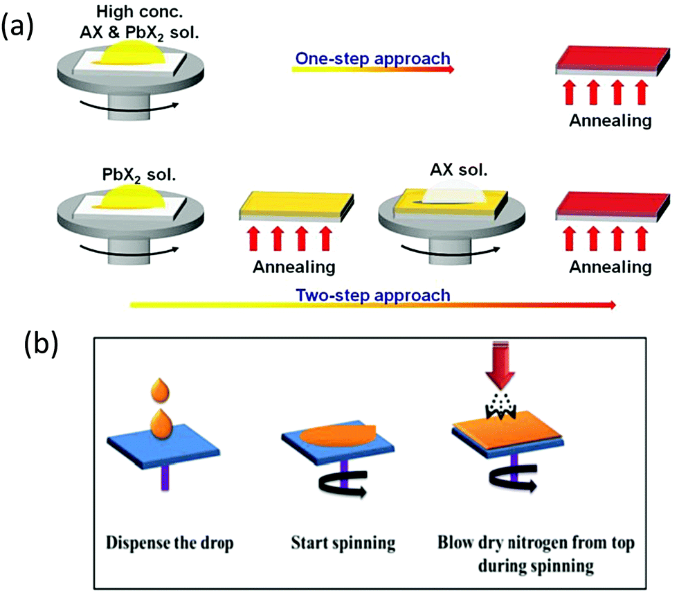 | ||
| Fig. 6 Representation of one-step and two-step strategies for the preparation of perovskite films. AX and PbX2 symbolize CsBr and PbBr2, respectively. Reprinted with permission ref. 106. Copyright 2019, The Royal Society of Chemistry. (b) N2 gas flow-assisted method for the fabrication of pinhole-free CsPbBr3 thin films. Reprinted from ref. 119. Copyright 2020, Gupta, Kulbak, and Cahen. | ||
Wang et al.107 fabricated the CsPbBr3 films via the one-step solution method by dissolving the precursors into the mixed DMF and DMSO solvents and reported the maximum concentration of only 0.4 M for the CsPbBr3 precursor solution. Also, the morphology of the films is affected by the one-step treatment as it is difficult to form uniform CsPbBr3 films via the one-step method. To tackle this issue, they suggested that if the evaporation rate of the solvent is slowed down, it can enhance the mass transport and diffusion, which could lead to a better film quality.
Generally, to prepare acceptable CsPbBr3 thin films, a mesoporous oxide substrate is used. However, to understand the fundamental properties for photovoltaic applications, it is important to use a regular substrate. Yu's118 and Gupta's groups119 adapted a gas flow-assisted process to deposit CsPbBr3 films on a regular substrate, as shown in Fig. 6c. This process involves the gas flow-assisted spin-coating process to deposit the perovskite precursor solution onto the flat substrate. The resulting films showed uniform behavior with increased density of the nucleation sites due to rapid cooling by solvent evaporation.
In recent years, several novel processing strategies such as vapor-assisted annealing, delayed annealing, and gas-blown anti-solvent washing have been introduced to significantly ameliorate the crystallization mechanism and to prepare uniform and pure CsPbBr3 films. Among these methods, solvent engineering is regarded as the most productive and easily functioning approach. As discussed earlier, choosing an appropriate solvent to dissolve PbBr2 and CsBr is a problematic step owing to their remarkable difference in solubility. While the two-step solution process does facilitate the preparation of CsPbBr3 films, the use of toxic solvents is a worrisome practice as toxic solvents such as methanol and DMF are commonly used, which may affect the health of research workers by permeating through the skin or respiration. A comprehensive research based on the use of different solvents for improving the uniformity and PCE, and decreasing the use of toxic solvents was made by Cao's group.112,122 As discussed in the previous section, water was used as a solvent to replace toxic methanol in the conventional two-step solution process.112 Although a promising PCE of 6.12% was achieved, the first step still involved the use of DMF to dissolve PbBr2. To overcome this issue, they further developed a solution process based on the formation of the PbBr2 solution from a mixed green solvent of polyethylene glycol (PEG) and γ-butyrolactone (GBL). A promising PCE of 8.11% was realized with the device configuration of FTO/TiO2/CsPbBr3/carbon. Furthermore, a series of green solvents such as acetone, anisole, water, ethanol, acetic acid, isopropyl alcohol, and ethyl acetate were employed for the extraction of residual PEG200, followed by a reaction with CsBr to form the CsPbBr3 films. It can be clearly seen that acetic acid as an anti-solvent resulted in the formation of a yellow CsPbBr3 film with smooth morphology. The SEM images of the CsPbBr3 films with different anti-solvents also suggested that using acetic acid as an anti-solvent resulted in pinhole-free and uniform film morphology with full coverage (Fig. 7a). The photographs of the prepared films with different green solvents are shown in Fig. 7b. In the commonly adopted two-step process, the fundamental issue of unavoidable CsPb2Br5 and Cs4PbBr6 impurity phases establishes a long-lasting bottleneck that hinders the prospective of CsPbBr3-based PSCs. To enable the formation of the pure CsPbBr3 phase in the Cs–Pb–Br system, it is important to control the precursor stoichiometry at both the macroscopic and molecular scales. Recently, this aforementioned issue was resolved via the solvent engineering strategy, as reported by Feng et al.123 In this strategy, they replaced conventionally used methanol with 2-methoxyethanol as the solvent to precisely control the CsBr:PbBr2 ratio and prepared phase-pure CsPbBr3 films. In contrast to the methanol-derived films, 2-methoxyethanol (EGME) solvent-assisted films demonstrated insignificant phase variation over the film matrix (Fig. 7c). Furthermore, with the regulation of crystal growth, stoichiometric and high quality CsPbBr3 films with reduced electron trap density were realized. Using the bi-solvents of EGME and isopropanol (IPA) instead of EGME, pure phase, compact, and smooth CsPbBr3 films were prepared, and a PCE of 7.29% was obtained for the PSCs with the structure of FTO/c-TiO2/CsPbBr3/carbon.243 More importantly, the crystal growth of solution-deposited devices can be effectively tuned by solvent engineering.
 | ||
| Fig. 7 (a) SEM micrographs of the Cs–Pb–Br films prepared using various solvent dropping methods. (b) The photographs of the Cs–Pb–Br films fabricated from PbBr2/(PEG + 40% GBL) using various solvent dropping methods. Reproduced with permission ref. 122. Copyright 2020, Wiley-VCH. (c) Representation of the conversion mechanism from the PbBr2 precursor film to the Cs–Pb–Br films in the methanol-based two-step process. Reproduced with permission ref. 123. Copyright 2020, Elsevier Ltd. (d) Multi-step solution method via the dipping process of the CsPbBr3 film (e) UV-vis absorption and PL spectra of the as-prepared CsPbBr3 films. Reproduced with permission ref. 117. Copyright 2018, American Chemical Society. | ||
To enhance the performance of the PSCs, it is essential to control the crystallization dynamics. Therefore, a more feasible approach is required to inhibit the decomposition of the precursor films in the solution and to improve the crystallization dynamics of the CsPbBr3 perovskite. However, inhibiting the decomposition of the CsPbBr3 thin-film is a great challenge in the conventional two-step solution process. At the initial stage, sequential dipping methods were employed to fabricate CsPbBr3 films in mesoscopic PSCs. However, the fabricated films decomposed rapidly in the precursor solution and showed poor morphology. Teng et al.117 proposed an elegant face-down liquid-space-restricted process to inhibit the decomposition of CsPbBr3. As a consequence, highly reproducible, smooth, and uniform films with large grain size of about 860 nm were obtained. The schematics of the face-up dipping process and face-down liquid-space-restricted process are depicted in Fig. 7d. The first step involves the deposition of the PbBr2/DMF solution via spin-coating onto the TiO2 layer at 2000 rpm for 30 s. After drying the substrate on a hot plate at 80 °C for 30 min, the PbBr2 films were face-down and face-up dipped in a methanol solution, followed by annealing the dried films at 250 °C for 5 min to obtain the CsPbBr3 films. It is noteworthy that in conventional two-step solution methods, the CsPbBr3 films decomposes quickly in the CsBr/methanol solution unlike that in the presented case. Furthermore, the optical investigation of the films via both the processes showed an emission peak at 527 nm. However, the films prepared by the face-down approach showed higher PL intensity than the films prepared by the face-up approach, as shown in Fig. 7e. Similarly, the face-down processed film showed much higher absorption intensity than the face-up processed film. It can be concluded that the films prepared with the face-down approach have fewer defects and higher crystallinity. Moreover, the planar CsPbBr3 PSC with carbon electrode prepared via the face-down approach showed a promising efficiency of 5.86% with a Voc of 1.34 V.
To further tackle the solubility issues of bromide in conventional solvents, Luo's group121 reported a novel Br2 vapor-assisted CVD process to realize fast anion-exchange from unstable CsPbI3 to stable CsPbBr3. In this method, iodides were selected as the raw materials to prepare the CsPbI3 films by spin-coating, followed by fast transformation into CsPbBr3via Br2 vapor-assisted method (Fig. 8a–c). Here, the CsPbI3 precursor was heated to 150 °C in a tube furnace and the Br2 vapors were introduced into the hot quartz tube. The reaction time of the transformation process was optimized and the light green-yellow CsPbI3 transformed into the bright yellow CsPbBr3 film. The reported methods give interesting insights into the fabrication of multiple compositions such as CsPb(I1−xBrx)3 with the optimization of the reaction conditions and the injection dose of the Br2 vapor. Li et al.120 developed a vapor-assisted solution method to prepare high quality and pure CsPbBr3 films. This method involves the deposition of the PbBr2/DMF solution via the spin-coating process, followed by the vapor-assisted deposition of CsBr onto the PbBr2 in a vacuum, as shown in Fig. 8d.
 | ||
| Fig. 8 (a) Br2 vapor extraction from a bottle of Br water; (b) schematics of the Br2 vapor-assisted CVD process; and (c) crystal structure. Reproduced with permission ref. 121. Copyright 2018, Elsevier Ltd. (d) Illustration of the evaporation-assisted solution method (EAS) to prepare a CsPbBr3 thin film. Reproduced with permission ref. 120. Copyright 2019, American Chemical Society. | ||
 | ||
| Fig. 9 (a) Schematics of the deposition process on (1) FTO with (2) c-TiO2, (3) m-TiO2, (4) PbBr2, and multistep deposition of CsBr. Reproduced with permission ref. 113. Copyright 2018, Wiley-VCH. (b) Illustration of the modified preparation process of the CsPbBr3 films. Reproduced with permission ref. 114. (c) An illustration presenting the conversion of PbBr2 into perovskites at various temperatures as well as perovskite compression. Reproduced with permission ref. 115. (d) Preparation mechanism of the integrated CsPbBr3/J61–ITIC device with the cross-sectional SEM image and the molecular structures of J61 and ITIC. Reproduced with permission ref. 116. Copyright 2019, Elsevier. (e) Illustration of the preparation procedure of the CsPbBr3 films with the PbBr2 films treated with the CB antisolvent. (f) XRD and UV-vis spectra of the CB-treated absorption spectra of the CsPbBr3 films treated by the CB antisolvent. Reproduced with permission ref. 231. Copyright 2019, Elsevier. | ||
4.2 Vacuum/vapor methods
The vapor processing of the perovskite films enables researchers to understand the properties of perovskites by precisely controlling the film thickness and fabricating highly reproducible PSCs with high efficiency. Vacuum deposition approaches involve the sublimation of CsX and PbX2 precursors in a vacuum chamber and provide fine thickness control and film homogeneity. One of the benefits of vacuum deposition approach is that it does not require a solvent, which eliminates the risk of solvent damage to the underlying layer. Generally, vacuum thermal evaporation consists of single source and multi-source evaporation processes. As discussed earlier, the fabrication of CsPbBr3 perovskite films via solution-based techniques is a challenge for large scale commercialization. Nevertheless, vacuum/vapor deposition approaches offer high reproducibility but the energy requirements related to vacuum processing are quite high and could impede the benefit of the rapid energy payback time of halide perovskites. Therefore, cost-effective vapor fabrication approaches should be developed for the fabrication of compact and large area CsPbBr3 perovskite films. Compared with the solution-based approaches, there are relatively few investigations discussing non-solution approaches for the preparation of CsPbBr3 films. In this section, we will discuss the potential non-solution fabrication approaches for the fabrication of high-quality CsPbBr3 films.:1–1.2:1). The deposited films showed extreme uniformity and optimum conditions was achieved at a substrate temperature of 300 °C, post-annealing temperature of 500 °C for 15 s, and evaporation rate of CsBr to PbBr2 of 0.7:1. Furthermore, these conditions were applied to fabricate CsPbBr3 solar cells with device architecture of FTO/c-TiO2/CsPbBr3/spiroMeOTAD/Au; a high filling factor of 78% and a promising PCE of 6.95% were achieved. Chen et al.125 reported a dual-source vacuum evaporation (DSVE) process for the fabrication of pinhole-free CsPbBr3 films with negligible grain boundaries and low defect concentration. Both the CsBr2 and PbBr2 precursors were simultaneously evaporated to avoid the vapor gas-like behavior and films with semi-transparent characteristics were obtained at a low evaporation rate. They found that the crystallinity and homogeneity of the CsPbBr3 films are highly dependent on the evaporation rate (Fig. 10b). For example, when the evaporation rate was too high, the prepared film showed inhomogeneous behavior and low crystallinity, while a low evaporation rate facilitated homogenous film formation. The resultant opaque planar PSC exhibits an ultrahigh open-circuit voltage of 1.44 V and the highest reported PCE of 7.78%. Unfortunately, the PCE of the vacuum/evaporation-processed CsPbBr3 devices is still lower than that of solution-processed devices owing to the fact that it is problematic to control the two precursors’ homogenous reaction with each other so as to render a precise 1:1 M ratio.
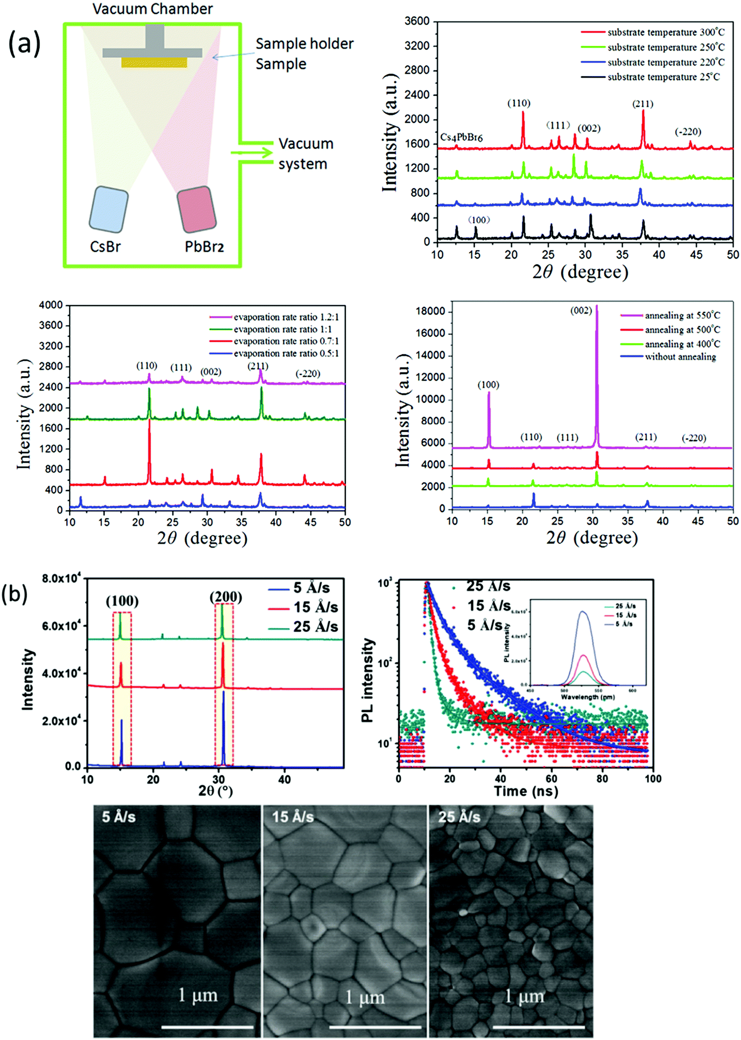 | ||
| Fig. 10 (a) Representation of the vacuum dual-source thermal co-evaporation process for the preparation of CsPbBr3 films. Reproduced with permission ref. 124. Copyright 2020, Elsevier Ltd. (b) Corresponding SEM micrographs of the CsPbBr3 films evaporated at different rates. Reproduced with permission ref. 125. Copyright 2018, Wiley-VCH. | ||
 | ||
| Fig. 11 (a) XRD spectra of CsBr powder, PbBr2 powder, a heated mixture of CsBr and PbBr2 powder, and the deposited CsPbBr3 film for 0.9:1 M ratio without substrate heating. (b) Mechanism of single-source thermal evaporation of CsBr and PbBr2 for the deposition of the CsPbBr3 film. Reproduced from ref. 127. Copyright, Elsevier. (c) XRD patterns, (d) AFM amplitude images, and (e) absorbance spectra of the films converted into CsPbBr3 by 60 min annealing at 100 °C: (a) soon after annealing, (b) after 50 days in a dry box, (c) after 50 days in a DH/atmosphere, and (d) after 5 days in 60% ≤ RH ≤ 80% and 19 ≤ T ≤ 23 °C. Reprinted from ref. 244. Copyright, 2020 NASI. (f) Representation of pulsed laser deposition approach (g) J–V curves and the device structure of the champion CsPbBr3 devices. Reproduced with permission ref. 133. Copyright 2019, American Chemical Society. | ||
Another promising alternative of solution-based methods is pulsed laser deposition (PLD), which offers low cost, suitable operation, and preparation of high-quality perovskite films by controlling the deposition conditions such as the vacuum pressure and substrate temperature. Using this process, Wang and coworkers133 fabricated high-quality and densely-packed CsPbBr3 films, which showed outstanding stability under high humidity conditions (Fig. 12e and f). They also suggested that CsPbB3 can completely penetrate in the m-TiO2 layer owing to the collisions among the ions with TiO2 particle surfaces. Pulsed laser deposited films were utilized as photoactive layers in CsPbBr3 PSCs, attaining ultrahigh Voc of 1.37 V, fill factor (FF) of 72%, and a promising efficiency of 6.3%.
 | ||
| Fig. 12 (a) Single-source vacuum thermal evaporation deposition. Reproduced with permission ref. 127. (b) Diagram of the S-DSVD and (c) MS-DSVD process for the deposition of the perovskite film. (d) Corresponding SEM images of S-DSVD and the MS-DSVD deposited film. Reproduced with permission ref. 129. Copyright 2019, Elsevier Ltd. (d) MS-DSVD method for the deposition of the CsPbBr3 films and the pressure-assisted annealing process. Reproduced with permission ref. 126. Copyright 2020, The Royal Society of Chemistry. | ||
:PbBr2 to 12:8, uniform CsPbBr3 films with low defect densities can be achieved by the sequential evaporation method. By optimizing the thickness (500 nm), the fabricated CsPbBr3/carbon devices exhibited a champion PCE of 7.58%.131 The preparation conditions such as sintering also play an important part in the preparation of compact CsPbBr3 films with large grains. Xian et al.132 introduced a sequential evaporation technology based on a two-step sintering (TSS) strategy to fabricate CsPbBr3 perovskite films. The TSS strategy, which was carried out in a muffle furnace, comprises of two steps: (1) preparing the CsPbBr3 perovskite at 320 °C; (2) crystal growth of dense CsPbBr3 films and defect reformation via sintering. Firstly, CsBr and PbBr2 are thermally evaporated by controlling the evaporation rates onto the substrates in the vacuum chamber. Then, a two-step sintering process is carried out on the obtained films in the muffle furnace under ambient conditions. With the optimization of the sintering conditions, compact CsPbBr3 perovskite films with an average grain size up to 2 μm are obtained. Moreover, the TSS strategy prolonged the charge lifetimes due to the suppression of recombination mechanisms and defect reduction in the crystal. Furthermore, the CsPbBr3 devices based on the TSS strategy exhibited tremendous thermal stability and achieved a champion efficiency of 9.35% under 1 sun illumination, which is comparable to that of solution-processed CsPbBr3 devices.
Further, Hua et al.126 reported the pressure-assisted multi-step sequential dual-source vacuum deposition (MS-DSVD) method to prepare compact CsPbBr3 perovskite films (Fig. 12e). The effect of pressure on the crystallization of the CsPbBr3 film was explored by adjusting the vessel pressure from 2 MPa to 10 MPa. To compare the performance of the films, another CsPbBr3 film was prepared at the annealing temperature of 335 °C under a standard atmospheric pressure of 0.1 MPa. Not surprisingly, the morphology of the prepared film at standard atmospheric pressure showed prominent pinholes and small grains. However, with the increase in the vessel pressure to 10 MPa, the pinholes vanished and the grain size increased substantially owing to the complete reaction between the precursors. Further, planar CsPbBr3 devices with the architecture of FTO/c-TiO2/perovskite/carbon were prepared using the vessel pressure of 10 MPa and a champion PCE of 7.22% was achieved.
5. Device architecture
The architecture of organic–inorganic PSCs dictates the choice of materials, preparation methods for the materials, and compatibility between the components in the device. These characteristics make the device performance highly reliant on the device architecture, where the perovskite (PVK) layer is sandwiched between the electron transport layer (ETL) and the hole transport layer (HTL). Two major device architecture design of PSCs have been established so far, i.e., planar and mesoscopic structures. Planar architecture further exists in either the conventional (n–i–p) or inverted (p–i–n) configuration.69 In the mesoscopic configuration, the perovskite either forms an over-layer on top of the infiltrated oxide scaffold or it is presented as a thin layer that will sufficiently cover the oxide scaffold with the pores in the scaffold, as shown in Fig. 13. To reduce the interface charge recombination and to simplify the device deposition process, ETL, HTL-free devices have also been developed.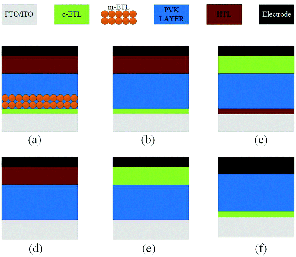 | ||
| Fig. 13 Main types of device structure of PSCs. (a) Regular mesoscopic structure. (b) Regular planar structure. (c) Inverted (planar) structure. (d) ETL-free structure. (e and f) HTL-free structure. | ||
Generally, TiO2,70,96 SnO2,71 ZnO,72 or phenyl-C61-butyric acid methyl ester (PCBM)73 are employed as ETLs, while spiro-OMeTAD (2,2′,7,70-tetrakis((N,N-p-dimethoxy-phenylamino)-9,90-spirobifl-uorene)),74,75 poly-[3-hexylthiophene-2,5-diyl] (P3HT),76,77 poly-triarylamine (PTAA),78,95 or NiOx79–97 are the commonly used as HTLs. Interestingly, both the planar and mesoporous architectures display considerable stability and performance. Moreover, the inverted PSCs shows less hysteresis as compared with the conventional ones.
Although both these types of PSCs have shown tremendous growth in the last decade, the stability concerns related with them is a stumbling block in their commercialization. Therefore, all-inorganic perovskite materials, such as CsPbX3, with high stability have become a hot topic in research.
6. CsPbBr3-based PSCs
One of the exceptional characteristics of CsPbBr3-based PSCs is their high Voc thanks to the wide bandgap of 2.3 eV with the optical absorption range of about 300–540 nm. Owing to its high stability, CsPbBr3 was the first lead halide perovskite material to be investigated as a light harvester. Kulbak and coworkers64 first fabricated the CsPbBr3 PSCs using different HTMs including spiro-OMETAD and PTAA in a device structure of FTO/c-TiO2/m-TiO2/CsPbBr3/HTL/Au. A champion PCE of 5.95% was achieved by using PTAA HTL. Fascinated by their findings, they immediately fabricated CsPbBr3 PSC via the two-step sequential deposition technique and boosted the PCE to ∼6%, which was comparable to that of the MAPbBr3 PSC but with enhanced stability.86Crystal growth on the CsPbBr3 films can be enhanced by the annealing process, as suggested by Hoffman et al.134 By optimizing the thickness of the film and carefully tuning the concentration of the precursor, they achieved a PCE of 5.6%. However, CsPbBr3 is usually annealed at a high temperature of >250 °C, which not only reduces the selection of materials for other layers but also increases the processing cost of the solar cells, which limits their potential in flexible electronics. To alleviate this issue, Yan's group135 proposed a pyridine (Py)-assisted process and reduced the prerequisite annealing temperature of the CsPbBr3 film down to 160 °C and yielded an efficiency of 6.04%. However, in the year 2017, pyridine was identified as a carcinogen by the World Health Organization, which makes this strategy unsuitable for practical applications.
As previously discussed, several derivative phases such as CsBr-rich Cs4PbBr6 and PbBr2-rich CsPb2Br5 have been revealed in the peripheral of the CsPbBr3 film. Some reports suggest that the presence of these non-perovskite derivative phases can passivate the grain boundaries and the interfaces; however, excess of any phase will introduce defects, which will degrade the photovoltaic efficiency of the devices. By utilizing phase conversion among CsPbBr3–CsPb2Br5–Cs4PbBr6 and the multi-step processing of the films, the device efficiency was significantly improved to 9.7% (Fig. 14a).97 Jiang and coworkers128 also pointed out the benefits of the non-perovskite CsPb2Br5 phase in passivating the surface defects and increasing the grain size of CsPbBr3 PSCs. Owing to the reduced charge recombination, a device efficiency of 8.34% was achieved for the CsPb2Br5-based device prepared with a PbBr2:CsBr ratio of 1.1. Further, the device efficiency of CsPbBr3 PSCs was boosted to 9.81% by the one-step solvent growth strategy.107 By tuning the CsBr deposition time, reducing the carrier recombination, and accelerating the charge transfer, the PCE of CsPbBr3 PSCs based on HTL of manganese sulfide (MnS) was further improved up to 10.45% (Fig. 14b).120
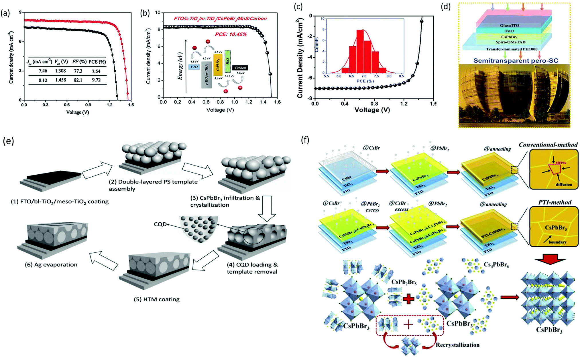 | ||
| Fig. 14 (a) The corresponding J–V curve of the CsPbBr3/carbon PSCs with and without GQDs. Reproduced with permission ref. 113. Copyright 2018, Wiley-VCH. (b) J–V characteristics of the PSCs with and without the MnS HTL. Reproduced with permission ref. 120. Copyright 2019, American Chemical Society. (c) EQE spectra of the fabricated pero-SC. (d) Image of the Soochow University library seen from the semitransparent CsPbBr3 device, inset: the device architecture of semitransparent pero-SCs. Reproduced with permission ref. 125. Copyright 2018, Wiley-VCH. (e) Fabrication mechanism of CQD/CsPbBr3 IO PSCs. Reproduced with permission ref. 150. Copyright 2017, Wiley-VCH. (f) Procedures for the fabrication of the CsPbBr3 thin film via conventional and phase transition induced (PTI) and the CsPbBr3 inorganic formation from the derivative phases. Reproduced with permission ref. 139. Copyright 2020. | ||
However, the drawback of such solution-based strategies is the low solubility of Br ions in the solvents as well as difficulties in controlling the over-rapid liquid-phase reaction and the imbalance between low densities of the heterogeneous nuclei, which ultimately produces non-uniform thin films. Liu's group124 further highlighted the influence of the substrate temperature, post-annealing temperature, and the ratio of evaporation rates in depositing uniform CsPbBr3 perovskite films. Through the tuning of these parameters, a stable PCE of 6.95% was achieved. Using the same method, Li's group125 fabricated opaque planar pero-structure CsPbBr3 PSCs and made significant improvement in the device efficiency, achieving a champion PCE of 7.78% with an ultrahigh Voc of 1.44 V (Fig. 14c). Fig. 14d shows that the architectural context can be clearly seen through the fabricated semitransparent CsPbBr3 device. Moreover, they further suggested that CsPbBr3, owing to its wide bandgap of 2.3 eV, can be an excellent choice for fabricating the top cell in tandem photovoltaic devices in order to improve their efficiency and stability. However, the device efficiency of vacuum-processed PSCs was much lower than that of the solution-processed CsPbBr3 PSCs.
Solution-processing approaches were also used to fabricate CsPbBr3 nanocrystals (NCs) and QDs films. The application of colloidal semiconductor nanocrystals (NCs) to fabricate optoelectronic devices is another promising strategy but it is a difficult task to transform the NCs solution to the NCs films by maintaining their properties. To overcome this issue, Akkerman's group136 reported a large-scale approach by employing low-boiling point ligands (propionic acid (PrAc) and butylamine (BuAm)) and ecologically-friendly solvents (isopropanol (IPrOH) and hexane (HEX)) for the preparation of CsPbBr3 NCs. They also suggested the importance of increasing the deposition cycles so as to promote the device efficiency and Voc of the CsPbBr3 PSCs. Based on the increase in thickness of 550 nm after 9 deposition cycles, an ultra-high Voc of 1.5 and a decent efficiency of 5.4% was obtained. Zhang et al.137 effectively improved the grain size of CsPbBr3 QDs by introducing the ligand solution treatment of NH4SCN/EA. A CsPbBr3–CsPb2Br5 composite film was formed by the ligand solution treatment, where Cs2PbBr5 can help in surface passivation and reduce the Br vacancies. The device efficiency improved to 6.81% by the incorporation of ZnO QDs as ETL and spiro-OMeTAD as HTL. By introducing a facile template-assisted spin-coating process, Zhou and coworkers150 developed a novel carbon quantum dot (CQD)-embedded CsPbBr3 inverse opal (IO) structure. The preparation protocol of CQD-embedded CsPbBr3 IO film is presented in Fig. 14e. The devices based on CQD-embedded CsPbBr3 IO film with the architecture of FTO/TiO2/CQD-perovskite IO/spiro-OMeTAD/Au generated a high efficiency of 8.29%, which was almost two times higher than that of planar structure devices.
Further, major progress was made by Tong's group139 with the development of conventional and phase transition induced (PTI) methods for the preparation of uniform CsPbBr3 films. In the PTI method, the CsPbBr3@CsPb2Br5 core–shell structured layer was first prepared by depositing CsBr and excess PbBr2, followed by the sequential vapor deposition of excess CsBr and PbBr2 to form the CsPbBr3@Cs4PbBr6 thin film. The phase transformation of the corresponding perovskites is shown in Fig. 14h. Based on the growth process induced by the phase transition strategy, a highly crystalline CsPbBr3 film with uniform grain-sizes and reduced trap density as well as lower surface potential barrier existing between the crystals and grain boundaries was obtained. A record efficiency of 10.91% was achieved for the n–i–p structured CsPbBr3-based PSCs, which is the highest reported PCE for CsPbBr3 devices till date. Moreover, the prepared devices exhibited excellent stability over 2000 h in high humidity conditions and 1400 h in 100 °C heating conditions. Such novel strategies, as proposed by Tong's group, should be further developed with special importance towards improving the film quality.
Despite extensive efforts, the device efficiency for CsPbBr3 PSCs is still comparatively lower than that of CsPbI3 PSCs, mainly due to wide-range absorption and defect states (Table 1). Therefore, the processing conditions of CsPbBr3 PSCs are of key importance to achieve a negligible defect state in order to trap photo-induced carriers. Within the perovskite, a majority of the intrinsic defects encourage a shallow transition level, while some defects with high formation energy will lead to deep transition levels, thus signifying the CsPbBr3 perovskite as a defect tolerance semiconductor with efficient photovoltaic response. We believe that further development should be made in enhancing the device efficiency by taking the advantage of the superior stability of CsPbBr3 perovskites.
| Device | Method | PCE | FF [%] | V oc [V] | J sc [mA cm−2] | Ref. |
|---|---|---|---|---|---|---|
| FTO/TiO2/CsPbBr3/SiQDs/spiro-OMeTAD/Ag | 1-Solution | 8.31 | 75 | 1.42 | 7.80 | 237 |
| ITO/SnO2/CsPbBr3/spiro-OMeTAD/Au | 1-Solution | 9.81 | 75.3 | 1.26 | 10.33 | 107 |
| FTO/m-TiO2/CsPbBr3/spiro-OMeTAD/Au | 2-Solution | 4.98 | 74 | 1.00 | 6.75 | 86 |
| FTO/m-TiO2/CsPbBr3/CBP/Au | 2-Solution | 4.92 | 54 | 1.32 | 6.91 | 86 |
| FTO/m-TiO2/CsPbBr3/PTAA/Au | 2-Solution | 5.72 | 73 | 1.27 | 6.16 | 86 |
| FTO/TiO2/CsPbBr3 QD/spiro-OMeTAD/Au | 2-Solution | 4.21 | 57 | 0.859 | 8.55 | 238 |
| FTO/TiO2/CsPbBr3/CZTS/spiro-OMeTAD/Ag | 2-Solution | 5.36 | 68 | 1.12 | 7.04 | 239 |
| FTO/TiO2/CsPbBr3/spiro-OMeTAD/Au | 2-Solution | 6.05 | 69 | 1.34 | 6.52 | 135 |
| FTO/TiO2/CsPbBr3(Cl)/spiro-OMeTAD/Ag | 2-Solution | 6.21 | 71.6 | 1.02 | 8.47 | 91 |
| FTO/ZnO/CsPbBr3–QDs/spiro-OMeTAD/Au | 2-Solution | 6.81 | 77.2 | 1.43 | 6.17 | 137 |
| FTO/TiO2/CsPbBr3/PTAA/Au | 2-Solution | 5.95 | 74 | 1.28 | 6.24 | 64 |
| FTO/TiO2/CsPbBr3/PTAA/Au | 2-Solution | 6.2 | 73 | 1.25 | 6.7 | 86 |
| TiO2/perovskite/Cu(Cr,Ba)O2 NCs/carbon | 2-Solution | 10.79 | 85.5 | 1.62 | 7.81 | 149 |
| FTO/TiO2/CsPbBr3/CuPc/carbon | 2-Solution | 6.21 | 74.4 | 1.26 | 6.62 | 91 |
| FTO/TiO2/SnO2/CsPbBr3/CuPc/carbon | 2-Solution | 8.79 | 81.4 | 1.31 | 8.24 | 95 |
| FTO/SnO2QDs/CsPbBr3/CsSnBr3 QDs/carbon | 2-Solution | 10.60 | 84.4 | 1.61 | 7.80 | 109 |
| FTO/SnO2QDs/CsPbBr3/CsBi2/3Br3 QDs/carbon | 2-Solution | 10.0 | 80.9 | 1.594 | 7.75 | 109 |
| FTO/SnO2QDs/CsPbBr3/CsCuBr3QDs/carbon | 2-Solution | 9.34 | 78.2 | 1.55 | 7.68 | 109 |
| FTO/TiO2/CsPbBr3/MnS/carbon | Solution and vapor | 10.45 | 83 | 1.52 | 8.28 | 120 |
| FTO/TiO2/CsPbBr3/spiro-OMeTAD/Au | Co-vapor | 6.95 | 78.5 | 1.27 | 6.97 | 124 |
| FTO/ZnO/CsPbBr3/spiro-OMeTAD/Au | Co-vapor | 7.78 | 77.11 | 1.44 | 7.01 | 125 |
| FTO/TiO2/CsPbBr3–CsPb2Br5/spiro-OMeTAD/Ag | Co-vapor | 8.34 | 75.9 | 1.30 | 8.48 | 128 |
| FTO/TiO2/PTI–CsPbBr3/spiro-OMeTAD/Ag | Sequential-vapor | 10.91 | 74.47 | 1.49 | 9.78 | 139 |
6.1 Role of HTL
Hole-transporting materials (HTMs) are an important part of PSCs that enable efficient extraction of photo-induced holes from the perovskite layer to the back electrodes. Throughout the literature, numerous types of HTMs have been employed to improve the device efficiency. Stability, and charge mobility.140–142 Discouragingly, these conventional HTMs offer unfavorable drawbacks such as high cost, low hole mobility or low conductivity, and instability, thus seriously hampering the practicable industrialization of the developing PSC technology. To boost the device efficiency of CsPbBr3 PSCs and future upscaling, novel, cost-effective, durable, and scalable alternative HTMs are suggested to be used. Recently, p-type Cu-phthalocyanine (CuPc) was used as an HTL for organic PSCs.143–145 The favorable effect of selecting CuPc as the HTM layer is that it can construct a Schottky barrier at the perovskite/electrode interfaces and reduce the carrier recombination, which will lead to fewer defects and pinhole-free film formation. Secondly, introducing the CuPc HTM layer will deliver a leveled energy-level transition, thus suppressing monomolecular recombination and trap states, which will be beneficial for improving the device efficiency of the PSCs.146,147 Liu's group66 incorporated CuPc as HTL in the CsPbBr3 PSCs and reported that CuPc can efficiently decrease charge recombination and facilitate charge transfer in CsPbBr3 PSCs. As shown by the PSCs models in Fig. 15a, the positive effects of the CuPc HTM layer is evident on the device process. Based on these favorable results, the optimized device yielded a promising PCE of 6.21%, which was 60% higher than the PCE of HTM-free PSCs. Further, CuPc was employed as an HTM for bilayer-structured CsPbBr3 devices, which not only resulted in improved stability but also boosted the PCE to 8.79% with a high Voc of 1.310 V and a FF of 0.814.95 | ||
| Fig. 15 (a) Illustration portraying the function of CuPc as an HTM in CsPbBr3 devices. Reproduced with permission ref. 114. Copyright 2018, Springer. (b) The corresponding SEM image portraying the multilayer FTO/TiO2/perovskite/HTM structure. (c) J–V characteristics of the corresponding devices. Reproduced with permission ref. 148. Copyright 2018, The Royal Society of Chemistry. (d) J–V curves of CsPbBr3 PSCs with Cu(Cr,M)O2 nanocrystals as the HTM. (e) Energy-level illustration of the corresponding devices for charge transfer process. Reproduced with permission ref. 149. Copyright 2018, Wiley-VCH. (f) Device structure and (g) the corresponding SEM image of the cells’ multilayer structure with FTO/c-TiO2/m-TiO2/perovskite/(MoO2/NC)/carbon structure. (h) Energy-level illustration corresponding to the CsPbBr3 devices. (i) The J–V curves under dark conditions. Reproduced with permission ref. 151. Copyright 2020, Elsevier Ltd. | ||
Although organic HTMs, as mentioned above, can facilitate hole extraction and decrease charge recombination for improving the device efficiency of CsPbBr3, the hygroscopic and unstable nature as well as the complex processing of organic HTMs is a major issue, which causes a negative impact on the long-term device stability. Recently, inorganic HTMs, together with high conductivity carbon materials, have shown promise in replacing expensive HTMs owing to their low-cost, easy processing, high-hole mobility, and non-hygroscopicity. This was further highlighted by introducing intermediate energy levels of MnS as the HTL to facilitate charge extraction in the CsPbBr3 device and to reduce electron–hole recombination.120 By optimizing the deposition thickness of CsBr and incorporating MnS as HTL, a high PCE of 10.45% was achieved, which was much higher than 8.16% for the device without HTL.
Zhao et al.148 introduced several HTLs such as PEDOT, PPy, and PANi in CsPbBr3 PSC with the device architecture of the m-TiO2/perovskite/HTL/carbon. The corresponding SEM micrographs in Fig. 15b exhibit a multi-layered structure with a well-defined boundary between each layer and an average thickness of 200 nm, 400 nm, and 15 mm for ETL, CsPbBr3, and the carbon electrode, respectively. Through systematic characterization, it was revealed that the incorporation of organic hole-transporting materials resulted in the suppression of charge recombination and improved charge extraction at the cell interfaces, which resulted in boosted device efficiency. A champion PCE of 9.32% 8.36%, 8.33% 7.69%, and 6.10%, was achieved for the BT-BTH, PEDOT, PPy, PANi, and HTM-free CsPbBr3 PSC, respectively (Fig. 15c). Duan et al.113 incorporated Cu(Cr,M)O2 (M = Ca2+, Ni2+, or Ba2+) nanocrystals as HTL for all-inorganic CsPbBr3 PSC. Owing to their enhanced hole-transporting characteristics, the device efficiency of the CsPbBr3 PSCs increases to 8.41% with the addition of the CuCrO2 layer, which further increased to 9.44%, 10.18%, and 10.03% with the incorporation of Cu(Cr,Ni)O2, Cu(Cr,Ba)O2, and Cu(Cr,Ca)O2 layers, and to 10.79% with the doping of Sm3+ ions (Fig. 15d). In addition, the graded energy-level alignment, as shown in Fig. 15e, is favorable for robust charge carrier collection. Zong et al.151 introduced an HTL of the MoO2/N-doped carbon nanosphere (NC) composite into the CsPbBr3/carbon PSCs to enhance the energy level alignment, regulate the work function, and charge extraction as well as to passivate the surface defects in the CsPbBr3 perovskite, to suppress the charge recombination and to reduce the energy loss at the interface. Fig. 15f and g exhibits the multilayer structure and the corresponding SEM micrograph of FTO/c-TiO2/m-TiO2/CsPbBr3/(MoO2/NC composites)/carbon. Energy level diagrams of the CsPbBr3 PSC indicate that the transition of the photo-generated electrons occurs from the valence band (VB) of CsPbBr3 to the conduction band (CB) and then drift into the CB of the ETL, causing the holes to transfer to the HTMs and the C-electrode (Fig. 15h). Further, the incorporation of MoO2/NC composites was beneficial as they reduced the energy loss and interface energy offset. By optimizing the N concentration in the MoO2/NC composite, the optimized device delivered a PCE of 9.40% in comparison to the reference device efficiency of 6.68% and showed excellent stability over 800 h in ambient conditions with RH = 80% (Fig. 15i).
6.2 Role of ETL
Similar to HTL, ETL is equally important and plays a vital role in inhibiting electron transfer and functionalizing hole extraction in PSCs. An ideal ETL with appropriate band structure, low trap state, good conductivity, and high density electron mobility is a prerequisite for maximizing the device efficiency of CsPbBr3 PSCs. However, limited research has been done to exploit the characteristics of commonly used ETL such as TiO2 and ZnO in order to minimize charge recombination in the CsPbBr3 film. One of the major issues is the large energy barrier at the interface between TiO2 (ECB = −4.24 eV) and the CsPbBr3 perovskite (ECB = −3.3 eV), which restricts electron transportation from the perovskite to the TiO2 layer. Moreover, the conduction band offset (CBO) between the ETL and the perovskites have a significant impact on interface recombination in the perovskite devices.For example, the CBO between the commonly used ETL TiO2 and CsPbBr3 is ∼0.94 eV, which deviates from the optimal range and thus limits the Voc and the performance of the CsPbBr3 PSCs. Recently, Cao et al.152 proposed a novel strategy for the preparation of CsPbBr3 PSC by employing Sr-modified TiO2 as the ETL for reducing the conduction band offset. The decrease in the conduction band offset efficiently enables the extraction of electrons from the perovskite to the ETL and as a result, the charge recombination significantly decreases. Based on these results, the carbon-based CsPbBr3 PSCs yielded a PCE of 7.22%, which is much greater than the efficiency of 5.92% for the controlled device (Fig. 16a). Further, Xu et al.153 boosted the mobility and electronic conductivity of the CsPbBr3 film by incorporating the antimony (Sb) dopant into the lattice of low-temperature processed TiO2 nanocrystals. The CsPbBr3 devices based on the Sb-doped TiO2 ETL yielded a Voc of 1.654 V, a champion PCE of 8.91%, and reduced hysteresis from 32% to 15% owing to the suppressed charge recombination and improved perovskite film quality (Fig. 16b–d).
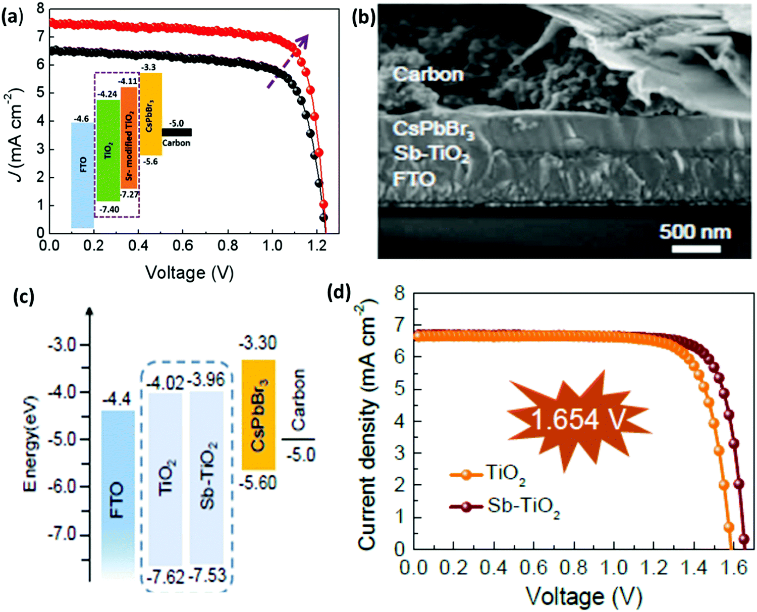 | ||
| Fig. 16 (a) J–V characteristics of the best performing devices with the inset showing the energy band diagrams of devices based on the Sr–TiO2 ETL layer. Reproduced with permission ref. 152. Copyright 2020, Elsevier Ltd. (b) The corresponding SEM image and (c) the representation of the energy-level diagram for CsPbBr3 planar devices. (d) The characteristic J–V curves based on TiO2 and Sb–TiO2 ETLs. Reproduced with permission ref. 153. Copyright 2020, The Royal Society of Chemistry. | ||
6.3 HTM-free CsPbBr3 PSCS
Although HTM-based CsPbBr3 PSCs have shown a relatively enhanced device efficiency, the device stability is still limited using organic HTMs. The conventionally used electrodes such as Au and Ag156 can be employed as hole extraction electrodes in HTM-free CsPbBr3 devices. However, in comparison with these electrode materials, carbon is economical, water-resistant, and inert towards ion migration originating from the perovskite and the metal electrodes, which makes it a promising electrode material for CsPbBr3 PSCs.153In comparison with conventionally used electrodes such as Ag or Au, carbon is preferred due to the following reasons: (i) using an ultra-thick carbon electrode can improve the stability of PSC as it remarkably reduces H2O/O2 penetration.154 (ii) The HTL is the most expensive part in a PSC, which can be overcome by employing carbon as an electrode material. (iii) The hole extraction and current conduction is effectively improved, which boosts the efficiency of PSC. (iv) Usual Ag or Au electrodes react easily with halide ions in the perovskite materials. (v) Carbon materials exhibit better water resistance and stability than Ag or Au.155 (vi) Carbon offers greater benefit for commercialization due to its reduced cost. (vii) Carbon possesses ideal work function with the VBM of the perovskite layer. (viii) Usual Ag or Au electrodes react easily with the halide ions in the perovskite materials. (ix) The sticky nature of the carbon paste helps in tolerating some amounts of pinholes in the perovskite films, which benefits by minimizing the defects, increasing the crystallinity, and producing films with larger grains. Presently, various carbonaceous allotropes,159 such as amorphous carbon,155 carbon nanotubes, graphite,157 and graphene,158 have been successfully employed in inorganic PSCs (Fig. 17a).
 | ||
| Fig. 17 (a) Carbonaceous allotropes’ structures. Reproduced with permission ref. 159. Copyright 2019, The Royal Society of Chemistry. (b) CsPbBr3 PSCs energy diagram. (c) The champion CsPbBr3 PSCs fabricated with and without IPA treatment. Reproduced with permission ref. 111. Copyright 2019, Elsevier Ltd. (d) Ideal charge generation with pure CsPbBr3 PSCs and combined with the derivative-phase PSCs. (e) The J–V characteristics of the corresponding champion cell. (f) The EQE spectrum and the corresponding integrated current of the best performing device. Reproduced with permission ref. 138. Copyright 2019, Wiley-VCH. (g) Energy level alignments representation for HTM-free CsPbBr3 PSCs. Reproduced with permission ref. 157. Copyright 2020, Elsevier Ltd. (h) Charge transfer mechanism of an FTO/c-TiO2/m-TiO2/perovskite/C device. Reproduced with permission ref. 163. Copyright 2019, The Royal Society of Chemistry. (i) J–V characteristics of the corresponding devices with various types of electrodes. Reproduced with permission ref. 164. Copyright 2020, The Royal Society of Chemistry. | ||
HTM-free CsPbBr3 PSC based on the architecture of FTO/TiO2/CsPbBr3/Au was first fabricated in 2015, yielding a promising PCE of 5.47%. HTM-free CsPbBr3 PSCs using a carbon electrode were first fabricated by Chang's group.64 By optimizing the reaction time and temperature, a promising efficiency of 5.0% was achieved. Further, Liang and coworkers87 boosted the PCE to 6.7% and achieved a high Voc of 1.24 V and FF of 0.73 using an FTO/TiO2/perovskite/C structure. The interesting part of these findings was the long-term stability of the prepared devices in the ambient conditions, which paved the way for further research on HTM-free CsPbBr3 PSCs. The carbon paste was also applied for HTM-free CsPb1−xMnxI1+2xBr2−2x PSCs, which yielded a PCE 7.36% of with excellent stability in ambient conditions.160 Liu's group161 proposed an efficient strategy for the fabrication of uniform CsPbBr3 films by introducing a porous CsPb2Br5 intermediate layer. They further highlighted the importance of using isopropanol (IPA) as the solvent for the low-concentration CsBr solution and in doing so, an ultra-high Voc of 1.38 V and a PCE of 6.1% were realized for the carbon-based PSC. Further, a facile two-step spin-coating process based on isopropanol-assisted post-treatment was again reported for the fabrication of highly efficient HTM-free CsPbBr3 perovskite films.111Fig. 17b shows the device structure, the corresponding SEM image, and the energy diagram of the corresponding CsPbBr3 devices. Based on the IPA-treated CsPbBr3 films, an ultra-high Voc 1.49 and one of the highest PCE of 8.11% for planar carbon-based CsPbBr3 PSCs was achieved (Fig. 17c). Presently, the highest PCE for CsPbBr3 is 10.91%, which was also realized by employing carbon paste as the electrode material.139 To further optimize the device efficiency, Ding and coworkers162 doped the PtNi alloy nanowires (NWs) (from 0 to 7 wt%) into the carbon ink in order to regulate the work function of the carbon electrodes. By optimizing the doping quantity of PtNi NWs (3 wt%), they achieved a champion PCE of 7.17%.
One major obstacle is the large recombination at the interface, which affects the photocurrent of the devices. To alleviate this issue, Tong's group138 further fabricated an HTL-free and gradient bandgap structure by introducing the CsPb2Br5 and Cs4PbBr6 derivative phases, which resulted in the boosting of the hole extraction efficiency and suppressed charge recombination at the interface. In this strategy, the derivative phase films were sandwiched between the ETL and carbon electrode layer, as shown in Fig. 17d. It was further suggested that the introduction of the derivative phases can produce the perfect charge generation/transport path for the PSC, as depicted in Fig. 17e. Eventually, a striking PCE of 10.17%, a Voc of 1.461 V, and photocurrent density of 9.24 mA cm−2 was realized through the CsPbBr3/CsPbBr3–CsPb2Br5/CsPbBr3–Cs4PbBr6 architecture approach with outstanding stability above 3000 h, retaining 85% of the original performance in ambient conditions and 700 h at 100 °C under thermal conditions, retaining 83% of the initial efficiency. Similarly, a wide plateau of over 80% in the range of 350 to 500 nm and a photo-current density near 7.4 mA cm−2 can be seen in the EQE spectrum of the champion device, which matches well with that of the absorption spectra (Fig. 17f).
Furthermore, Bu's group157 added polyaniline/graphite (PANi/G) into the carbon electrode to enhance the hole extraction and tailor the work function of the back electrode for improved energy level arrangement. This strategy led to a remarkable improvement in the interfacial hole extraction and suppressed the charge recombination and energy loss. In doing so, a striking PCE of 8.87% and Voc of 1.59 V was realized, which is 43.8% higher than 6.17% PCE for the control device (Fig. 17g).
Further, Liao et al.163 proposed a combination of multi-walled carbon nanotubes (MWCNT) and carbon black (CB) for a CsPbBr3/C-based PSC. By tuning the MWCNT/CB ratio, the electrical conductivity and work function (WF) of the carbon electrode was tuned to lessen the energy difference at the perovskite/carbon interface and to promote charge extraction. Based on this strategy, the 25 wt% champion device delivered a PCE of 7.62% and an outstanding stability at 80% RH (Fig. 17h). Recently, Mi et al.164 incorporated 1-D structured carbon nanotubes (CNTs) and 2-D Ti3C2–MXene nanosheets into the carbon paste to facilitate the multi-dimensional charge transfer path. Owing to the improved carrier extraction and transport, a respectable PCE of 7.09% was achieved for the carbon/CNT/MXene-mixed electrode in the CsPbBr3–PSCs (Fig. 17i).
Although promising results have been realized for HTL-free CsPbBr3 PSCs, the lethargic carrier dynamics accelerate substantial and unfavorable interfacial recombination arising from the large energy change between the CsPbBr3 perovskite and the carbon electrode, which is still a deficiency (Table 2). By introducing an HTL between the perovskite and carbon, a Schottky barrier can be established, which prevents the direct contact of carbon with the ETL through the pinholes, which can suppress carrier recombination. To overcome these issues, different intermediate level layers such as carbon and black phosphorus quantum dots, polyaniline (PANi), and poly(3-hexylthiophene) HTMs have been incorporated at the CsPbBr3/carbon interface to facilitate hole extraction and ameliorate the energy level alignment. Also, several strategies have been developed to overcome the severe energy losses at the perovskite/carbon interface and will be briefly discussed in the next section.
| Device | Method | PCE | FF [%] | V oc [V] | J sc [mA cm−2] | Ref. |
|---|---|---|---|---|---|---|
| FTO/m-TiO2/CsPbBr3/Au | 2-Solution | 5.47 | 74 | 1.21 | 6.21 | 86 |
| FTO/TiO2/CsPbBr3/C | 2-Solution | 5.86 | 68 | 1.34 | 6.46 | 102 |
| FTO/TiO2/CsPbBr3/C | 2-Solution | 6.1 | 62 | 1.38 | 7.13 | 161 |
| FTO/TiO2/CsPbBr3/C | 2-Solution | 6.7 | 73 | 1.24 | 7.4 | 32 |
| FTO/TiO2/CsPbBr3/C | 2-Solution | 8.63 | 82.22 | 1.37 | 7.66 | 241 |
| FTO/TiO2/CsPbBr3/C | 2-Solution | 9.72 | 82.1 | 1.458 | 8.12 | 113 |
| FTO/c-TiO2/m-TiO2/Cs0.98Li0.02PbBr3/C | 2-Solution | 7.87 | 77.9 | 1.45 | 6.95 | 220 |
| FTO/c-TiO2/m-TiO2/Cs0.94Na0.06PbBr3/C | 2-Solution | 8.31 | 80.0 | 1.49 | 6.97 | 220 |
| FTO/c-TiO2/m-TiO2/Cs0.92K0.08PbBr3/C | 2-Solution | 8.61 | 78.4 | 1.51 | 7.25 | 220 |
| FTO/c-TiO2/m-TiO2/Cs0.91Rb0.09PbBr3/C | 2-Solution | 9.86 | 82.2 | 1.55 | 7.73 | 220 |
| FTO/c-TiO2/m-TiO2/CsPb0.97Yb0.03Br3/C | 2-Solution | 9.20 | 80.2 | 1.54 | 7.45 | 230 |
| FTO/c-TiO2/m-TiO2/CsPb0.97Er0.03Br3/C | 2-Solution | 9.66 | 82.8 | 1.56 | 7.46 | 230 |
| FTO/c-TiO2/m-TiO2/CsPb0.97Ho0.03Br3/C | 2-Solution | 9.75 | 83.2 | 1.57 | 7.45 | 230 |
| FTO/c-TiO2/m-TiO2/CsPb0.97Tb0.03Br3/C | 2-Solution | 10.06 | 84.8 | 1.59 | 7.47 | 230 |
| FTO/TiO2/CsPb0.97Sm0.03Br3/C | 2-Solution | 10.14 | 85.1 | 1.59 | 7.48 | 230 |
| FTO/TiO2/CsPbBr3/C:PtNiNW | 2-Solution | 7.86 | 81.0 | 1.432 | 6.78 | 162 |
| FTO/TiO2/CsPbBr3/C | Solution and vapor | 5.38 | 70 | 1.13 | 6.79 | 240 |
| FTO/c-TiO2/CsPbBr3/CsPbBr3–CsPb2Br5/CsPbBr3–Cs4PbBr6/C | Co-vapor | 10.17 | 75.39 | 1.461 | 9.24 | 138 |
| FTO/TiO2/CsPbBr3/C | Co-vapor | 8.86 | 80.4 | 1.52 | 7.24 | 129 |
6.4 CsPbBr3 nanoparticles (NPs) in PSCs
Recently, there has been an increased interest in the preparation of CsPbX3 nanoparticles (NPs) for photovoltaic devices. Owing to their high absorption coefficient, high carrier mobility, tunable bandgap, low conduction band minimum (CBM), and high PL quantum yields (PLQY), it is believed that the introduction of CsPbX3 nanoparticles (NPs) can facilitate the electron transport from the photoactive layer to the electrode layer.252–255 Moreover, literature reports suggest that the CsPbX3 nanoparticles (NPs) are more stable than their perovskite films, which make them interesting candidates to be employed in photovoltaic applications. Previously, MAPbBr3−xIx nanocrystals were introduced into the perovskite layer and the HTL to enhance hole extraction and to regulate the band structure of the perovskite.256 However, MAPbBr3−xIx (NPs) suffers from poor chemical stability, which hinders their application potential in PSCs. Compared with organic (NPs), inorganic (NPs) such as CsPbBr3 show excellent chemical stability and hold great potential for improving the device efficiency and stability when incorporated into the photoactive layers. As CsPbBr3 possesses much higher stability, thus it is less challenging to prepare CsPbBr3 (NPs) as compared with CsPbI3. Recently, Gao et al.257 introduced CsPbBr3 (NPs) to the chlorobenzene anti-solvent in order to control the perovskite film growth towards low defects, large grain sizes, and improved crystallinity of the MAPbI3 films. The incorporation of CsPbBr3 (NPs) resulted in improved device efficiency with the optimized device exhibiting a high PCE of 20.46% with improved stability and low hysteresis. Chen et al.258 introduced a CsPbBr3@SiO2 (NPs) coating for efficient and stable PSCs. This strategy resulted in the suppression of charge recombination and boosted the UV utilization. In doing so, the device efficiency of the photoactive layer was enhanced from 19.7% to 20.8%, which is a 5.6% improvement from that of the uncoated PSC. In addition, the CsPbBr3@SiO2 (NPs)-coated device exhibited negligible hysteresis and could effectively block light-induced degradation, thus improving the lifetime over 100 h under UV illumination for the perovskite devices. These studies show that the incorporation of CsPbBr3 (NPs) is a feasible strategy for improving charge collection and extraction, diminishing the high charge recombination, and reducing the grain boundaries.7. Engineering technologies
The spectral response range of the CsPbBr3 perovskite can be widened by substituting partial Br− with I− to boost the device efficiency. However, in doing so, the device stability of CsPbBr3 is greatly affected. Therefore, the suppression of charge recombination is regarded as an efficient strategy to improve the device performance and to maintain the inherent stability of the CsPbBr3 perovskite. Within the perovskite films, a larger part of the charge recombination arises at the grain boundaries as they induce a shallow state presence near the valence band (VB) edge of the perovskite, which restricts hole diffusion and offers sites for the position of many uncoordinated ions defects.165,166 Therefore, the fabrication of dense and uniform CsPbBr3 films with low grain boundaries and defect states is an essential requirement for realizing high-efficiency PSCs with improved stability. Remarkable research effort has been put in developing different technologies such as additive engineering, anti-solvent engineering, as well as compositional and interface engineering to suppress charge recombination and reduce grain boundaries in perovskite films (Fig. 18). | ||
| Fig. 18 Strategies for boosting the device efficiency of CsPbBr3 perovskites. | ||
7.1 Additive engineering
The classical crystallization theory may be one of the promising approaches, which incorporates functional additives into the precursor solution to achieve compact and uniform perovskite films by regulating the crystallization dynamics and achieving the passivation of uncoordinated ions defects. Additive engineering is considered as an effective method for simultaneously annihilating the ionic traps as well as increasing the grain size of the photoactive layers.167,168 To enhance the quality of perovskite films, a variety of additives including ammonium salts,169,170 nanoparticles,171 polymers,167 Lewis acid or base,172 and ionic liquids173,174 have been employed to the precursor solution so as to bond with the halogen ionic defects and uncoordinated Pb2+. Previously, Yang et al.175 reported an improvement in the PCE from 18.77% to 20.84% for MAPbI3 perovskite due to defect passivation and regulation of the crystal orientation with additive engineering. Huang and coworkers176 developed a new passivation molecule of D-4-tert-butylphenylalanine (D4TBP) and incorporated it into the precursor solution for the preparation of uniform perovskite films with suitable grain size and low defect states, achieving an improved efficiency up to 21.4% of the p–i–n structured devices.Zhu and coworkers177 introduced a commonly available additive melamine in the PbBr2 precursor solution to passivate the defects and simultaneously develop the crystal growth of CsPbBr3 perovskite films. They found that the crystallinity of PbBr2 is effectively reduced with the introduction of melamine and a high quality, pinhole free, large grain size CsPbBr3 film is prepared (Fig. 19a). Compared with the pristine film, the melamine-incorporated CsPbBr3 film exhibited low defects and significantly reduced the grain boundaries with an increase in the grain size from 682 nm to 945 nm. The VB of melamine-CsPbBr3 (−5.60, −5.58, −5.61, and −5.63 eV for 0.5%, 1%, 2%, and 4% melamine-CsPbBr3, respectively) is shifted up to approach the work function of carbon, indicating a decreased energy level difference between the CsPbBr3 layer and the carbon electrode, which promotes the transportation and extraction of holes and reduces energy loss (Fig. 19b). Moreover, the optimized CsPbBr3 device showed a striking Voc of 1.584V with a champion device efficiency of 9.65% compared to the PCE of 6.07% and Voc of 1.584 of the pristine device (Fig. 19c). Notably, the champion device exhibited long-lasting stability under high temperature and high humidity conditions.
 | ||
| Fig. 19 (a) Illustration of the crystallization process for CsPbBr3 film without and with melamine additive. (b) Energy level alignment of charge transfer process. (c) Steady-state power output curves of corresponding devices. Reproduced with permission ref. 177. Copyright 2020, Wiley-VCH. (d) Energy level alignment of the corresponding devices. Reproduced with permission ref. 178. Copyright 2020, Elsevier Ltd. (e) Top-view SEM images of the pure CsPbBr3 film and CsPbBr3–1.5% NH4SCN one. (f) J–V curves. Reproduced with permission ref. 179. (g) Energy-level diagram of the PSCs. Reproduced with permission ref. 180. Copyright 2020, American Chemical Society. | ||
Pei et al.178 modified a layer of BiBr3 as an additive on the PbBr2 film before the CsBr coating to fabricate uniform CsPbBr3 films. This strategy led to an improvement in the crystal quality as well as attuned the energy level so as to promote carrier extraction from the perovskite (Fig. 19d). As the result, the PCE was effectively improved to 8.73%. Recently, Wang et al.179 incorporated the NH4SCN additive into the precursor solution to prepare uniform CsPbBr3 perovskite films. It was suggested that films with low trap state density, good crystallinity, and reduced interface defects can be obtained by additive incorporation with NH4SCN. It is evident from Fig. 19e that the incorporation of NH4SCN additive led to a much flatter and cleaner surface compared to that of the pure one. Moreover, the energy-level alignment of the CsPbBr3–1.5% NH4SCN film is lower than that of the pure film, which indicates that the changed energy-level arrangement will not considerably influence the device performance. By optimizing the molar ratio of NH4SCN (1.5%), the CsPbBr3 device delivered a champion efficiency of 8.47%, which was higher than that of the controlled one (7.12%) (Fig. 19f). The device efficiency of the CsPbBr3 perovskite can be severely deteriorated due to the strong charge recombination arising from the ionic defects at the grain boundaries of the perovskite. To overcome this issue, Zhang et al.180 adopted the strategy of incorporating the amino acid of L-lysine with two amino and one carboxyl groups into the CsPbBr3 film to concurrently passivate the uncoordinated Pb2+ (Cs+) and halogen ion defects. The grain size of the films showed a significant improvement from 688 nm to over 1000 nm with the addition of L-lysine, which is attributed to the reduced nucleation rate and adequate growth of the perovskite, which decreases the grain boundaries. They found that by optimizing the concentration of the additive in the PbBr2 solution, the defect density is effectively reduced, the carrier life time is prolonged, and the interfacial energy level alignment is greatly enhanced, which adds to a greatly improved charge extraction and transfer (Fig. 19g). Moreover, the incorporation of L-lysine resulted in improved quality and suppression of charge recombination of the CsPbBr3 film, which is due to the development of the crystallinity of the film with the modulation of the surface morphology and reduced grain boundaries. Benefiting from these qualities, the photovoltaic efficiency of the optimized CsPbBr3 device was strikingly improved from 6.01% to 9.69%. Moreover, the encapsulated devices showed longer-lasting stability under high humidity and maintained nearly 95% of the efficiency at 80% RH and 25 °C for over 45 days.
All of these studies highlight the fact that additive incorporation is an effective approach for grain size improvement, suppression of charge recombination, and defect passivation so as to fully improve the device performance of the CsPbBr3 perovskite.
7.2 Interface engineering
Although additive engineering is a feasible strategy to reduce the defects and suppress charge recombination in CsPbBr3 PSCs, yet, it necessitates complicated optimization as the mixed system undergoes severe phase transition due to its thermodynamic driving force.181 Currently, new strategies such as interfacial engineering along with passivation methods have garnered significant attention due to manifold functions such as interface energy level compensation, surface defects passivation, and stability improvement. In the literature, the study on surface passivation of CsPbBr3 by polymers or other chemical compounds and the influence of interface modification on mismatched energy levels between the perovskite and the electrode is very scarce. To date, few interfacial engineering strategies such as the incorporation of inorganic salts,182,183 organic halide salts,184 electronic donor materials,185,186 or Lewis base polymers including polyvinylpyrrolidone187 have been employed to passivate the surface defects of the perovskite films for enhancing the PCE, lowering the Voc loss, and enhancing the stability.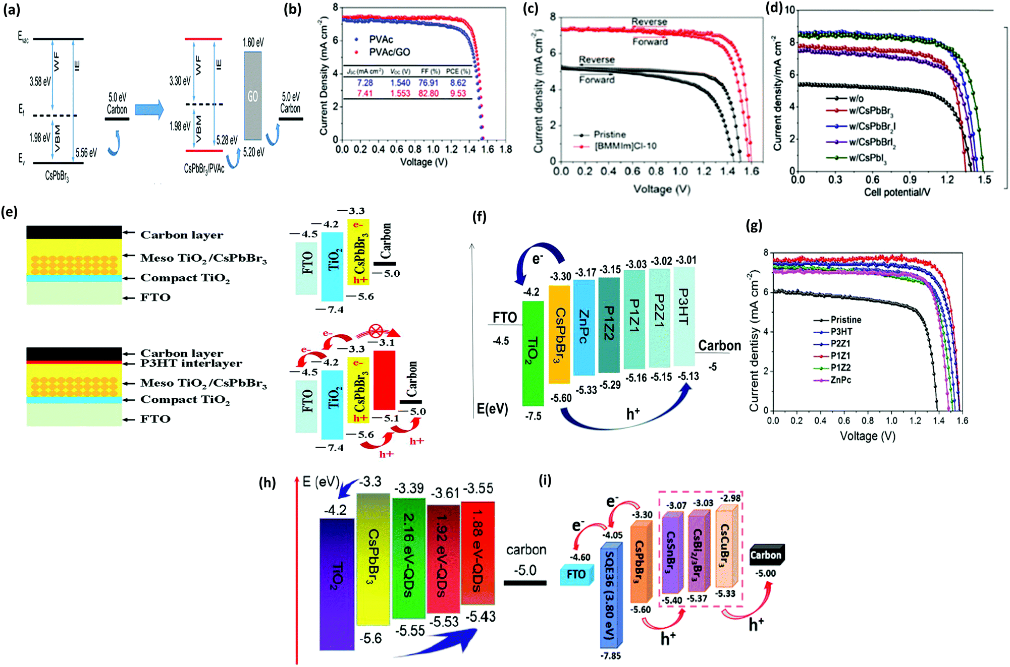 | ||
| Fig. 20 (a) Schematic illustration of the energy-level relationship of the CsPbBr3 layer with PVAc and GO modification. (b) J–V curves of the PVAc-modified CsPbBr3 solar cells with and without GO. Reproduced with permission ref. 188. Copyright 2019, American Chemical Society. (c) J–V curves of [BMMIm]Cl− incorporated and pure CsPbBr3 devices. Reproduced with permission ref. 198. Copyright 2020, American Chemical Society, (d) The corresponding J–V curves of the CsPbBr3 solar cells with and without CsPbBrxI3−x NCs. Reproduced with permission ref. 199. (e) Diagram of the cross-sectional structure and the energy level alignment of the CsPbBr3 PSCs without and with the P3HT interlayer. Reproduced with permission ref. 201. Copyright 2019, Elsevier Ltd. (f) Energy level alignment of the materials in the PSC and (g) the photocurrent–voltage (J–V) curves of CsPbBr3 PSCs with and without HTMs. Reproduced with permission ref. 209. Copyright 2019, The Royal Society of Chemistry. (h) Energy level alignment of each layer in the device. Reproduced with permission ref. 218. Copyright 2018, The Royal Society of Chemistry. (i) Energy level alignment of the PSC with the structure of FTO/SQE/CsPbBr3/CsMBr3/carbon. Reproduced with permission ref. 219. Copyright 2019, Wiley-VCH. | ||
However, the unfortunate part of using P3HT as the HTM is the inferior hole mobility compared to that of spiro-OMeTAD, which reduces the PCE of the PSCs. To boost the carrier mobility, several organic, inorganic, and polymeric materials have been incorporated to P3HT to form the composite HTMs.202–207 To date, a promising photovoltaic efficiency of 17.8% with excellent stability has been realized for phthalocyanine HTM devices, making it a promising candidate for composite HTMs.208 Based on these findings, Liu et al.209 incorporated a cost-effective and organic-semiconducting material zinc phthalocyanine (ZnPc) with an appropriate lowest unoccupied molecular orbital (LUMO) energy level of about −3.17 eV as well as the highest occupied molecular orbital (HOMO) energy level of about −5.33 eV into P3HT by tuning the mass ratios via solution fabrication to enhance the hole mobility of P3HT and optimize the energy level to match well with the CsPbBr3 perovskite (Fig. 20f). The ZnPc/P3HT composite was employed as the HTM for PSCs with the device architecture of FTO/c-TiO2/m-TiO2/perovskite/ZnPc/P3HT/C. The incorporation of ZnPc with P3HT not only down-shifted the HOMO energy level and effectively enhanced the hole mobility of P3HT but also the surface defects states of the CsPbBr3 perovskite were passivated. Due to the well-matched energy level and higher hole mobility, the optimized cell prepared in ambient conditions showed a short-circuit current density (Jsc) of 7.652 mA cm−2, an ultra-high Voc of 1.578 V, FF of 83.06%, and a high PCE of 10.03% with outstanding stability in ambient conditions (Fig. 20g).
Based on these findings, it is suggested that introducing an intermediate layer of composite HTMs is a feasible strategy for passivating the surface defects and optimizing the energy level difference as well as enhancing the device efficiency and stability of CsPbBr3 PSCs.
Previous studies suggest that defects on the surface of traditional semiconductors can be significantly passivated by incorporating a shell on the surface of the QD, which leads to improved photoluminescence (PL) and quantum efficiency.217 Li et al.218 successfully fabricated core–shell constructed QDs on the CsPbBr3 device, which exhibited outstanding photovoltaic properties including tunable energy levels and high luminescence and realized a champion PCE of 8.65%, which was 14.8% higher than that of the pristine cell (Fig. 20h). The same group further developed quantum interfacial engineering by setting an intermediate energy-level at the CsPbBr3/perovskite with CsSnBr3−xIx quantum dots (QDs). Their study suggested that maximized charge extraction can be achieved by tuning the Br:I ratio of the CsSnBr3−xIx quantum dots (QDs). By doing so, a champion PCE of 9.13% and excellent stability in high humidity conditions (80% RH or 80 °C) over 720 h is realized for the CsSnBr2I QDs-tailored CsPbBr3 device. The benefit of selecting CsSnBr3−xIx quantum dots (QDs) as interfacial modification materials is their similar processing prerequisites to those of the CsPbBr3 perovskite layers. They also introduced graphene quantum dots and CuInS2/ZnS QDs for the interfacial modification of CsPbBr3/carbon interface, which led to the enhanced PCE of 9.72% and 8.42%, respectively.218 Recently, tin-oxide (SnO2) QDs have been reported as promising electron transporting material owing to their high electron mobility, high transparency, wide bandgap, and good photostability, as suggested by Zhao et al.219 By incorporating SnO2 QDs as the ETL and CsMBr3 (M¼Sn, Bi, Cu) QDs as the HTL between the CsPbBr3 layer and carbon electrode, better energy level alignment was realized, which contributed to the fast electron–hole separation and suppressed charge recombination, leading to an improved PCE of 10.6% and ultra-high open-circuit voltage of up to 1.610 V for CsPbBr3 PSCs (Fig. 20i). Although quantum dots’ interfacial engineering presented promising results, the introduction of HTMs at the interface is regarded to be a more suitable strategy due to the limited hole extraction ability of the quantum dots.
7.3 Precursor engineering
The quality of the perovskite films is a critical factor for increasing the efficiency of the solar cells. Therefore, designing high-quality pinhole-free films that possess large grain size with monolayer alignment is the key procedure in the preparation of highly efficient CsPbBr3 devices. As discussed earlier, most of the preparation of CsPbBr3 films is based on solution-based technologies. Therefore, the preparation of high-quality CsPbBr3 films with a highly concentrated precursor (CsBr, PbBr2) solution is a prerequisite for photovoltaic applications via solution-based methods. However, the low solubility of CsBr in commonly used solvents such as DMF and DMSO is a challenging step to prepare the CsPbBr3 film via solution methods with optimum thickness. The dilemma of low solubility of CsBr was previously discussed and solved through precursor engineering.81 A facile single-step solution method using highly soluble cesium acetate (CsAc) and hydrogen lead trihalide (HPbX3) was developed to tackle the aforementioned Cs-precursor solubility limitation and to prepare high-quality α-CsPbX3 perovskite films. Uniform and ultra-smooth CsPbX3 perovskite films were obtained at relatively low temperature due to the strong interaction between the CsAc and HPbX3 induced precursors. However, the fabricated CsPbBr3 devices delivered a low PCE of 5.96%, indicating that further optimization of the films is required.Further study based on novel-precursor engineering strategy was developed by Huang et al.106 by using a precursor pair of cesium acetate (CsAc) and ionic liquid methylammonium acetate (MAAc) so as to enhance the concentration of the CsPbBr3 precursor solution to 1.0 M, obtaining high quality and large grain sized CsPbBr3 films (Fig. 21a). It is well-known that most of the acetates such as lead acetate (PbAc2) are considered as promising precursors due to their good solubility in conventional solvents such as (DMF) and (DMSO). It was suggested that using this precursor strategy, the film quality is substantially improved: (i) the crystallization dynamics can be tailored with the incorporation of the MAAc ionic liquid to the precursor solution due to strong interaction between Ac− and Pb2+; (ii) the limitation of low concentration of the precursor solution is resolved by the introduction of highly soluble CsAc and a thickness of up to 600 nm is obtained. Correspondingly, with the implementation of this strategy, the trap state-related charge recombination was suppressed and improved light harvesting capacity with a champion PCE of 7.37% with a high fill factor of 0.841 was achieved.
 | ||
| Fig. 21 (a) Mechanism of CsAc/MAAc-based CsPbBr3 film crystallization kinetics. Reproduced with permission ref. 106. Copyright 2019, The Royal Society of Chemistry. (b) The corresponding J–V curves of CsPbBr3 PSCs based on various perovskite absorbers. Reproduced with permission ref. 230. Copyright 2018, Wiley-VCH. (c) Statistical grain size distribution. Reproduced with permission ref. 232. Copyright 2019, The Royal Society of Chemistry. (d) Cross-sectional SEM image of the corresponding devices. (e) Band alignment of all-inorganic PSC with the CsPb1−xTMxBr3 layer. (f) The representative J–V curves of the CsPbBr3 PSCs based on various perovskite absorbers. Reproduced with permission ref. 223. Copyright 2019, Elsevier Ltd. (g) J–V curves of different alkali metal cation-doped PSCs. Reproduced with permission ref. 224. Copyright 2018, Wiley-VCH. (h) Characteristic J–V curves measured under simulated AM1.5G sun light of 100 mW cm−2 irradiance. Reproduced with permission ref. 251. Copyright 2018, Nature. (i) Characteristic J–V curves of pure and Cl-doped CsPbBr3 PSCs. Reproduced with permission ref. 236. Copyright 2020, Wiley-VCH. | ||
7.4 Compositional engineering
Compositional engineering of doping hetero-ions in the host lattice has been broadly developed as an efficient approach to improve the PCE of CsPbBr3 PSCs. It has been demonstrated that the partial replacement of the Cs-site with alkali metal cations (Na+, Li+, K+, and Rb+) and the Pb-site with transition metal cations (Mn2+, Zn2+, Cu2+, Co2+, etc.), or rare earth cations such as Ln3+ in the perovskite lattice of CsPbBr3 is a preeminent strategy to improve the grain size of the perovskite with low trap states and suppression of charge recombination in order to boost the device efficiency.220,221 Previously, Liu et al.222 systematically examined the effect of Cs-site cations on the device performance, suggesting that the quality of the films can be enhanced by the doping of alkali metal cations. The incorporation of alkali metal cations in the perovskite lattice passivated the grain boundaries, enhanced the grain size, suppressed the non-recombination losses, and increased the built-in potential, which substantially improved the device efficiency. Previous studies have shown that large grain sizes of CsPbBr3 and CsPbBr2I can be realized with the incorporation of alkali metal cations (e.g., Li+, Na+, K+, and Rb+) at the Cs+-site for low trap state density and charge recombination. In addition to Cs-site doping, the incorporation of homovalent or hetrovalent ions at the Pb2+-site also causes a passivation effect on the perovskite grains. The non-recombination rate can also be suppressed with the partial replacement of Pb2+ by lanthanide ions (Sm3+, Tb3+, Ho3+, Er3+, and Yb3+) as well as the partial incorporation of In3+, Al3+, Ca2+, Cd2+, and Sr2+, as suggested by literature reports.225–229Duan's group230 also proposed a compositional engineering approach to boost the efficiency of CsPbBr3 by the lattice incorporation of lanthanide ions (Ln3+ = La3+, Ce3+, Nd3+, Sm3+, Eu3+, Gd3+, Tb3+, Ho3+, Er3+, Yb3+, and Lu3+) into perovskite films. The partial introduction of lanthanide ions not only enhanced the grain size but the carrier lifetime was also considerably prolonged and charge recombination within the perovskite was greatly reduced. By tuning the stoichiometric ratio of the dopants, a promising efficiency of 10.14% with a Voc of 1.594 V was achieved for the HTM-free PSC with the FTO/c-TiO2/m-TiO2/CsPb0.97Sm0.03Br3/C architecture, which is considerably higher than the 6.99% efficiency of the pristine CsPbBr3 device (Fig. 21b). Moreover, the doped fabricated devices exhibited good long-term moisture stability under harsh humidity conditions (RH 80%) in air atmosphere for over 110 days and sustained thermal-tolerance at 80 °C for over 60 days. These findings offer new prospects for endorsing the commercialization of highly efficient CsPbBr3 PSCs with long-term stability.
However, the unfortunate part of lanthanide ions’ incorporation is that they are predominantly located at the grain boundaries of the perovskite film apart from the incorporation into the perovskite lattice by a small quantity during the formation of the CsPbBr3 perovskite due to the higher metal ionic values, which restricts the better understanding of the film quality and substitution of the Pb2+-sites with extrinsic ions in the perovskite lattice. In their recent study,232 the same group further addressed this issue by incorporating divalent hard Lewis acids cations (M = Mg2+, Ca2+, Sr2+, and Ba2+) in the CsPbBr3 perovskite lattice. It is evident from the average grain size histogram of the doped CsPbBr3 that the grain size substantially increased to 870 nm as compared with that of the pristine CsPbBr3 film. It is comprehensible that the grain size is mostly enhanced due to the suppressed crystal nucleus formation (Fig. 21c). Moreover, in comparison with the pristine sample, the surface roughness of the hard Lewis acid cations-doped CsPbBr3 films is substantially lowered. To the best of our knowledge, lower grain boundaries can markedly reduce the defect state and therefore increase the device efficiency of the perovskite. Based on these outcomes, a high PCE of 9.63% was realized for the optimal cell with the FTO/c-TiO2/m-TiO2/CsPb0.97Sr0.03Br3/C architecture, which is greater than the PCE of 7.25% for the undoped cell. Tang et al.223 further employed the compositional engineering strategy by partially incorporating the divalent transition metal ions (TM2+ = Mn2+, Ni2+, Cu2+, and Zn2+) with smaller ionic radius at the Pb2+ site to regulate the crystalline structure for HTM-free carbon-based CsPbBr3 PSCs. Noticeably, the CsPbBr3 films showed large grains with low grain boundaries due to the incorporation of divalent transition metal ions (Fig. 21d). Moreover, the performance of the carbon-based CsPbBr3 devices improved significantly due to low trap state density and there was a reduction in the energy loss in the charge carrier transfer (Fig. 21e). Also, the incorporation of the TM2+ ions undoubtedly suppressed the charge recombination at the CsPbBr3/carbon interface. Benefitting from these findings, the optimized Zn-doped film exhibited a champion PCE of 9.18% with excellent stability of over 760 h in high humidity conditions (RH 80%) (Fig. 21f). Similar results were reported by Li's group224 by means of doping the CsPbBr3 perovskite with various alkali metal cations. They reported that the lattice dimensions and energy levels of the Cs1−xRxPbBr3 (R¼Li, Na, K, Rb, x¼0–1) perovskite can be optimized by adjusting the Cs/R ratio. According to their systematic investigations, it was suggested that the introduction of alkali metal cations can bring promotional effects on the CsPbBr3 perovskite such as the shrinking of the lattice, electrical energy distribution, and crystallized dynamics. Furthermore, owing to the decreased charge-trap state, a high efficiency of 9.86% was realized for the HTM-free Cs0.91Rb0.09PbBr3 device with enhanced air stability (Fig. 21g).
It is well known that halide regulation (Cl and I) is a feasible strategy, by which the optical and photo-physical characteristics of the CsPbBr3 perovskites can be successfully tuned. As the CsPbBr3 PSCs possess superior stability and ultra-high Voc, the significant loss in the Jsc is a critical factor that hinders the photovoltaic performance. Compositional engineering of the halide ions can be incorporated to tune the photovoltaic performance of CsPbBr3-based PSCs. C. H. N. and coworkers251 reported the compositional engineering of CsPbBr3 perovskites and highlighted the role of iodine incorporation into the CsPbBr3−xIx perovskite. The addition of iodine resulted in a slight improvement in the device efficiency from 2.97% to 3.98% with a high Voc of 1.13 V (Fig. 21h). Obviously, with the incorporation of iodine, the bandgap descended and the hysteresis performance of the CsPbBr2.9I0.1 perovskite solar cell, as compared to the CsPbBr3 device, was successfully mitigated. Besides the doping of iodine ions, the doping of chloride anion has also been studied as an effective dopant for regulating the perovskite films with enlarged grains for low defects and ameliorating the crystalline quality of the perovskite film. Moreover, chloride anion substitution promotes the transport of charge carriers, which reduces the trap state density by promoting the transport of charge carriers, which decreases the trap state density of the perovskite.233–235 Inspired by these findings, Li et al.236 prepared Cl-doped CsPbBr3 films via the multistep solution method to improve the charge extraction and separation of the perovskite and to reveal the effect of chlorine doping on the mobility rate of the carriers and interfacial energy level matching in the CsPbBr3 system. Their findings suggested that doping chlorine not only suppresses charge recombination in the device but also improves the grain size, carrier mobility, and energy level alignment at the interface, leading to enhanced charge extraction and transportation as well as increased carrier lifetime within the cells. Based on these findings, the optimized chlorine-doped cell with the structure of FTO/c-TiO2/m-TiO2/CsPbBr2.98Cl0.02/C exhibited an ultra-high Voc of 1.571 V and a PCE of 9.73% was realized, which is a striking enhancement in comparison with the Voc of 1.479 and PCE of 6.69% for the pristine device (Fig. 21i).
8. Conclusion and prospects
Since the pioneering report in 2015, CsPbBr3 has been a research hotspot in the photovoltaics community. After several years of development, all-inorganic CsPbBr3 PSCs have accomplished the highest efficiency of 10.91%, approaching approximately 70% of the Shockley–Queisser (SQ) efficiency limits. The significant advances in the device efficiency are accredited to the superior thermal and moisture stability of the CsPbBr3 perovskite. However, there is a large research space that is needed to be filled out to match the PCE of other counterparts, whose PCEs are over 80% of the SQ limits. Owing to the high bandgap of 2.3 eV, the S–Q limit model of CsPbBr3 indicates a maximum PCE of 16.5%. Similarly, the theoretical calculations show a Voc of 1.98 V, which is much higher than the highest stated Voc of 1.615 V for CsPbBr3 PSCs. In this review, we have systematically discussed the different aspects of CsPbBr3 PSCs, starting with the basic properties to the development of different methodologies and engineering strategies to increase the stability and enhance the photovoltaic performance of CsPbBr3 PSCs. Unlike other halide perovskites, CsPbBr3 does not suffer from stability issues; however, there is plenty of room for further development for achieving higher PCE. We believe that the following research directions could be beneficial for further enhancing the photovoltaic performance of CsPbBr3 devices.(i) The future advances of CsPbBr3 perovskites necessitate the thoughtful design and preparation of each essential functional layer, such as the perovskite layer and the interfaces, and careful selection of the electron transport layer (ETL) and the hole transport layer (HTL) for controlling the carrier dynamics, suppression of charge recombination, and reducing the energy losses. We believe that extensive research is required to overcome the difficult challenge of designing optimal interfaces for stable and efficient CsPbBr3 solar cells, which should fulfil the following merits: (i) have optimal surface energy; (ii) possess proper energy level alignment to decrease the energy barrier for charge transfer; (iii) efficient charge extraction; (iv) can passivate the films’ trap-state densities; (v) facilitates low-temperature processing and compact and pinhole-free film formation; (vi) high stability.
(ii) ETL and HTL are an important part of the PSCs structure, which can effectively accelerate carrier transport and reduce carrier recombination, thus contributing to improved device performance and stability. The development of ETL and HTL with optimal energy levels can significantly facilitate charge transfer. Secondly, the quality of the perovskite crystal structures plays a significant role as crystal structures with fewer defects enhance the carrier lifetime and reduce the energy losses in the perovskite. However, organic HTL, in particularl, spiro-OMeTAD, contributes to high cost as well as instability of the CsPbBr3 PSCs. Moreover, the use of traditional ETLs such as TiO2 contributes to the short lifetimes caused by the UV-induced instability, thus affecting the photovoltaic performance of the CsPbBr3 PSCs. We suggest that other alternative ETLs and HTLs should be developed and special attention should be given to the ETL/perovskite interface and the HTL/perovskite interface in order to boost carrier transport. For the optimization of the transport layers, there are few critical points such as such as energy level alignment, trap states, morphology, charge mobility, and interfacial properties, which are crucial for shaping the final performances of the devices. The energy level alignment between the transport layers and the perovskite can efficiently accelerate the carrier transport to enhance the Jsc and FF. Moreover, the well-matched Fermi levels will contribute to enhanced Voc of the CsPbBr3-based devices. Therefore, it is important to develop new and effective strategies such as compositional engineering and interfacial engineering to passivate the interfacial defects and suppress non-radiative recombination.
(iii) In order to achieve compact and uniform CsPbBr3 films, the following merits should be fulfilled: (i) have adequate thickness; (ii) pinhole-free and compact nature; (iii) good phase purity. Solution-based methods offer cost-effective and easy processing strategies but the unfavorable part is the low solubility of solvents, followed by several physical conditions relating to different factors such as vapor pressure, composition stoichiometry, boiling point, and dielectric constant, which should be fulfilled so as to resolve the possible incompatibility between solution-based processes and large area fabrication. For example, conventionally used solvents such as pure DMSO and DMF cannot meritoriously improve the solubility of the precursors for gaining a thick film. Using such solvents for the preparation of the CsPbBr3 perovskite not only slows down the crystallization process but also affects the film morphology. Therefore, we suggest that new environment-friendly solvents should be employed and their mechanism of crystal growth and role in intermediate formation should be comprehensively investigated.
(iv) We believe that the fabrication approach should have the following merits in order to be considered for industrial-scale fabrication: (i) low cost; (ii) excellent reproducibility; (iii) feasible for large areas. However, the development of large-scale processing technology has become a serious issue that must be taken care of before industrialization. The commonly used solution methods such as drop-casting and spin-coating are unfavorable for large scale fabrication. Vapor/vacuum-based and printing methods are much more favorable for scale-up and large area devices. Presently, there have been limited studies on large active areas and a majority of fabricated PSCs have been reported for small active areas (<1 cm2). It still remains a challenging task to scale up the size of the CsPbBr3 PSCs without substantial efficiency loss.
(v) Furthermore, a variety of state-of-the-art engineering strategies such as compositional engineering, additive engineering, interfacial engineering, and precursor engineering have been established to enhance the photovoltaic performance of the CsPbBr3 PSCs. We believe that the different engineering strategies mentioned in this review will positively influence the stability, film morphology, and PCE efficiency of the CsPbBr3 PSCs. The reason for this is evident from the massive improvement in the device efficiency from 5.74 to 10.91% in a short period, which has been realized with the optimization of the crystal growth process, suppression of carrier recombination, and improved carried transport. It is also put forward that strategies such as doping and additive engineering of inorganic CsPbBr3 facilitates the improvement in the stability as well as the reduction in the trap-state densities and suppression of charge recombination at the interface, thus contributing to the improvement of the device efficiency of CsPbBr3 perovskites. Unfortunately, limited research attention has been paid to such strategies; thus, it is required to further develop and modify such new and existing strategies so as to boost the efficiency of CsPbBr3 PSCs. It is suggested that introducing new materials as interface materials or as additives can reduce the surface defects and passivate the grain boundaries, thus improving the PCE and stability of the perovskite.
(vi) Apart from HTL-based CsPbBr3 PSCs, stable electrode materials such as carbon have been employed to replace the conventional electrodes such as Ag, Au, and expensive HTMs for HTL-free CsPbBr3 PSCs. The advances in carbon-based CsPbBr3 PSCs show great promise in fulfilling the criteria of the golden triangle, i.e., (i) high PCE, (ii) low cost, and (iii) high stability. For example, the carbon electrode not only facilitates charge extraction but also offers device encapsulation function. Moreover, the development of carbon-based or HTM-free CsPbBr3 PSCs have good prospect in meeting the challenge of large scale and low-cost fabrication and thus, should be further explored. However, the shortcomings of HTM-free PSCs need to be further studied before they can be considered as a permanent replacement to HTM-based PSCs.
(vii) Furthermore, we believe that strengthening the basic theoretical concepts through theoretical simulations and modeling are important for explaining the experimental results. The simulated device structures can provide important information about the materials and thickness of each layer, which can be further employed as a convincing reference for the experiments. Recently, our group242 optimized the working mechanism of the CsPbBr3 perovskite using simulation analysis and introduced a gradient junction design of the absorber, which resulted in the effective reduction in high interface recombination and an ultra-high open-circuit voltage (Voc) of 1.68 V; a record high PCE of 11.58% was realized for modulated CsPbBr3 PSCs. Our findings propose that significant research efforts are still needed for the further improvement in the device efficiency as well as the open-circuit voltages of CsPbBr3 PSCs.
(viii) To make the CsPbBr3 perovskite feasible for flexible application, we believe that it is important to fabricate PSCs at low processing temperatures so as to accelerate the charge transport and to passivate the defects. For this purpose, it is important to understand the mechanism of crystal growth at low temperatures and to develop ways to decrease the activation energy of crystal growth without relinquishing the crystal quality. Since CsPbBr3 has a large bandgap, combining with smaller bandgap photovoltaic materials to fabricate tandem solar cell can be a promising strategy for the further development of highly efficient tandem devices. We believe that the hybrid tandem solar cells based on CsPbBr3 PSCs have great prospect and will generate more research attention in the future.
(ix) Long-term stability has been a major concern for other organic–inorganic PSCs such as CsPbI3. Compared with its counterparts, CsPbBr3 exhibits good resistance against harsh humidity and thermal conditions. However, an essential consideration for large scale commercialization is the long-term operational stability of the CsPbBr3 PSCs, which needs further studies. For this purpose, it is important to understand the degradation mechanism of selective contacts and electrodes as interface-related chemical reactions at the perovskite/electrodes have been considered as the possible cause for the degradation of the photovoltaic performance of the CsPbBr3 PSCs. We suggest that the hydrophobic nature of the carbon electrode could be a game changer for prolonging the stability of CsPbBr3 PSCs.
Conflicts of interest
The authors declare that they have no known competing financial interests or personal relationships that could have appeared to influence the work reported in this paper.Acknowledgements
This work was supported by the Program for the Innovation Team of Science and Technology in University of Henan of China (No. 20IRTSTHN014).References
- D. M. Chapin, C. S. Fuller and G. L. Pearson, J. Appl. Phys., 1954, 25, 676–677 CrossRef CAS
.
- N. M. Haegel, R. Margolis, T. Buonassisi, D. Feldman, A. Froitzheim, R. Garabedian, M. Green, S. Glunz, H.-M. Henning, B. Holder, I. Kaizuka, B. Kroposki, K. Matsubara, S. Niki, K. Sakurai, R. A. Schindler, W. Tumas, E. R. Weber, G. Wilson, M. Woodhouse and S. Kurtz, Science, 2017, 356, 141–143 CrossRef CAS
- M. M. Lee, J. Teuscher, T. Miyasaka, T. N. Murakami and H. J. Snaith, Science, 2012, 338, 643–647 CrossRef CAS
- S. D. Stranks, G. E. Eperon, G. Grancini, C. Menelaou, M. J. P. Alcocer, T. Leijtens, L. M. Herz, A. Petrozza and H. J. Snaith, Science, 2013, 342, 341–344 CrossRef CAS
- G. E. Eperon, S. D. Stranks, C. Menelaou, M. B. Johnston, L. M. Herz and H. J. Snaith, Energy Environ. Sci., 2014, 7, 982–988 RSC
- Z. Shi, Y. Li, Y. Zhang, Y. Chen, X. Li, D. Wu, T. Xu, C. Shan and G. Du, Nano Lett., 2017, 17, 313–321 CrossRef CAS
- Z. Shi, S. Li, Y. Li, H. Ji, X. Li, D. Wu, T. Xu, Y. Chen, Y. Tian, Y. Zhang, C. Shan and G. Du, ACS Nano, 2018, 12, 1462–1472 CrossRef CAS
- A. Kojima, K. Teshima, Y. Shirai and T. Miyasaka, J. Am. Chem. Soc., 2009, 131, 6050–6051 CrossRef CAS
- W. S. Yang, B. W. Park, E. H. Jung, N. J. Jeon, Y. C. Kim, D. U. Lee, S. S. Shin, J. Seo, E. K. Kim, J. H. Noh and S. I. Seok, Science, 2017, 356, 1376–1379 CrossRef CAS
- E. H. Jung, N. J. Jeon, E. Y. Park, C. S. Moon, T. J. Shin, T.-Y. Yang, J. H. Noh and J. Seo, Nature, 2019, 567, 511–515 CrossRef CAS
- Q. Jiang, Y. Zhao, X. Zhang, X. Yang, Y. Chen, Z. Chu, Q. Ye, X. Li, Z. Yin and J. You, Nat. Photonics, 2019, 13, 460–466 CrossRef CAS
- M. Kim, G.-H. Kim, T. K. Lee, I. W. Choi, H. W. Choi, Y. Jo, Y. J. Yoon, J. W. Kim, J. Lee, D. Huh, H. Lee, S. K. Kwak, J. Y. Kim and D. S. Kim, Joule, 2019, 3, 2179–2192 CrossRef CAS
- J. Burschka, N. Pellet, S. J. Moon, R. Humphry-Baker, P. Gao, M. K. Nazeeruddin and M. Gratzel, Nature, 2013, 499, 316–319 CrossRef CAS
- H. Zhou, Q. Chen, G. Li, S. Luo, T.-b. Song, H.-S. Duan, Z. Hong, J. You and Y. Yang, Science, 2014, 345, 542–546 CrossRef CAS
- N. J. Jeon, J. H. Noh, W. S. Yang, Y. C. Kim, S. Ryu, J. Seo and S. I. Seok, Nature, 2015, 517, 476–480 CrossRef CAS
- W. S. Yang, J. H. Noh, N. J. Jeon, Y. C. Kim, S. Ryu, J. Seo and S. I. Seok, Science, 2015, 348, 1234–1237 CrossRef CAS
- https://www.nrel.gov/pv/assets/pdfs/best-research-cellefficiencies.20190802.pdf .
- K. O. Brinkmann, J. Zhao, N. Pourdavoud, T. Becker, T. Hu, S. Olthof, K. Meerholz, L. Hoffmann, T. Gahlmann, R. Heiderhoff, M. F. Oszajca, N. A. Luechinger, D. Rogalla, Y. Chen, B. Cheng and T. Riedl, Nat. Commun., 2017, 8, 13938 CrossRef CAS
- S. Chen, X. Wen, S. Huang, F. Huang, Y.-B. Cheng, M. Green and A. Ho-Baillie, Sol. RRL, 2017, 1, 1600001 CrossRef
- Y. Guo, X. Yin, J. Liu, S. Wen, Y. Wu and W. Que, Sol. RRL, 2019, 3, 1900135 CrossRef
- G. Tong, X. Geng, Y. Yu, L. Yu, J. Xu, Y. Jiang, Y. Sheng, Y. Shi and K. Chen, RSC Adv., 2017, 7, 18224 RSC
- D. Shan, G. Tong, Y. Cao, M. Tang, J. Xu, L. Yu and K. Chen, Nanoscale Res. Lett., 2019, 14, 208 CrossRef
- L. K. Ono, E. J. Juarez-Perez and Y. B. Qi, ACS Appl. Mater. Interfaces, 2017, 9, 30197 CrossRef CAS
- E. J. Juarez-Perez, Z. Hawash, S. R. Raga, L. K. Ono and Y. B. Qi, Energy Environ. Sci., 2016, 9, 3406 RSC
- E. J. Juarez-Perez, L. K. Ono, M. Maeda, Y. Jiang, Z. Hawash and Y. B. Qi, J. Mater. Chem. A, 2018, 6, 9604 RSC
- B. Mi, H. Li, Z. Song, G. Zhao, G. Tong and Y. Jiang, NANO, 2017, 12, 1750150 CrossRef CAS
- J. Zhang, G. Hodes, Z. Jin and S. F. Liu, Angew. Chem., Int. Ed., 2019, 58, 2 CrossRef
- C. Dong, X. Han, W. Li, Q. Qiu and J. Wang, Nano Energy, 2019, 59, 553 CrossRef CAS
- Y. Wang, T. Zhang, M. Kan and Y. Zhao, J. Am. Chem. Soc., 2018, 140, 12345 CrossRef CAS
- Y. Wang, M. I. Dar, L. K. Ono, T. Zhang, M. Kan, Y. Li, L. Zhang, X. Wang, Y. Yang, X. Gao, Y. B. Qi, M. Grätzel and Y. Zhao, Science, 2019, 365, 591 CrossRef CAS
- Q. Wang, X. Zhang, Z. Jin, J. Zhang, Z. Gao, Y. Li and S. F. Liu, ACS Energy Lett., 2017, 2, 1479 CrossRef CAS
- J. Liang, C. Wang, Y. Wang, Z. Xu, Z. Lu, Y. Ma, H. Zhu, Y. Hu, C. Xiao, X. Yi, G. Zhu, H. Lv, L. Ma, T. Chen, Z. Tie, Z. Jin and J. Liu, J. Am. Chem. Soc., 2016, 138, 15829 CrossRef CAS
- K. Wang, Z. Jin, L. Liang, H. Bian, D. Bai, H. Wang, J. Zhang, Q. Wang and S. Liu, Nat. Commun., 2018, 9, 4544 CrossRef
- Y. Wang, X. Liu, T. Zhang, X. Wang, M. Kan, J. Shi and Y. Zhao, Angew. Chem., Int. Ed., 2019, 58, 16691–16696 CrossRef CAS
- J. Song, Q. Cui, J. Li, J. Xu, W. Yue, L. Xu, X. Jie, Y. Dong, T. Tian, H. Sun and H. Zeng, Adv. Opt. Mater., 2017, 5, 1700157 CrossRef
- Z. Yang, M. Wang, H. Qiu, X. Yao, X. Lao, S. Xu, Z. Lin, L. Sun and J. Shao, Adv. Funct. Mater., 2018, 28, 1705908 CrossRef
- P. Becker, J. A. Márquez, J. Just, A. Al-Ashouri, C. Hages, H. Hempel, M. Jošt, S. Albrecht, R. Frahm and T. Unold, Adv. Energy Mater., 2019, 9, 1900555 CrossRef
- E. M. Sanehira, A. R. Marshall, J. A. Christians, S. P. Harvey, P. N. Ciesielski, L. M. Wheeler, P. Schulz, L. Y. Lin, M. C. Beard and J. M. Luther, Sci. Adv., 2017, 3, eaao4204 CrossRef
- A. Ho-Baillie, M. Zhang, C. F. J. Lau, F.-J. Ma and S. Huang, Joule, 2019, 3, 938–955 CrossRef CAS
- W. Xiang and W. Tress, Adv. Mater., 2019, 31, 1902851 CrossRef CAS
- J. Wang, J. Zhang, Y. Zhou, H. Liu, Q. Xue, X. Li, C.-C. Chueh, H.-L. Yip, Z. Zhu and A. K. Y. Jen, Nat. Commun., 2020, 11, 177 CrossRef CAS
- W. E. I. Sha, H. Zhang, Z. S. Wang, H. L. Zhu, X. Ren, F. Lin, A. K. Y. Jen and W. C. H. Choy, Adv. Energy Mater., 2018, 8, 1701586 CrossRef
- X. Ren, Z. Wang, W. E. I. Sha and W. C. H. Choy, ACS Photonics, 2017, 4, 934–942 CrossRef CAS
- S. Rühle, Sol. Energy, 2016, 130, 139–147 CrossRef
- C. Li, X. Lu, W. Ding, L. Feng, Y. Gao and Z. Guo, Acta Crystallogr., Sect. B: Struct. Sci., 2008, 64, 702–707 CrossRef CAS
- C. C. Stoumpos, C. D. Malliakas, J. A. Peters, Z. Liu, M. Sebastian, J. Im, T. C. Chasapis, A. C. Wibowo, D. Y. Chung, A. J. Freeman, B. W. Wessels and M. G. Kanatzidis, Cryst. Growth Des., 2013, 13, 2722 CrossRef CAS
- C. K. MøLler, Nature, 1958, 182, 1436 CrossRef
- G. Li, H. Wang, Z. Zhu, Y. Chang, T. Zhang, Z. Song and Y. Jiang, Chem. Commun., 2016, 52, 11296 RSC
- F. Palazon, S. Dogan, S. Marras, F. Locardi, I. Nelli, P. Rastogi, M. Ferretti, M. Prato, R. Krahne and L. Manna, J. Phys. Chem. C, 2017, 121, 11956 CrossRef CAS
- I. Dursun, M. De Bastiani, B. Turedi, B. Alamer, A. Shkurenko, J. Yin, A. M. El-Zohry, I. Gereige, A. AlSaggaf, O. F. Mohammed, M. Eddaoudi and O. M. Bakr, ChemSusChem, 2017, 10, 3746–3749 CrossRef CAS
- H. Yang, Y. Zhang, J. Pan, J. Yin, O. M. Bakr and O. F. Mohammed, Chem. Mater., 2017, 29, 8978–8982 CrossRef CAS
- K. H. Wang, L. Wu, L. Li, H. B. Yao, H. S. Qian and S. H. Yu, Angew. Chem., Int. Ed., 2016, 55, 8328–8332 CrossRef CAS
- Y. Zhang, M. I. Saidaminov, I. Dursun, H. Yang, B. Murali, E. Alarousu, E. Yengel, B. A. Alshankiti, O. M. Bakr and O. F. Mohammed, J. Phys. Chem. Lett., 2017, 8, 961–965 CrossRef CAS
- M. I. Saidaminov, J. Almutlaq, S. Sarmah, I. Dursun, A. A. Zhumekenov, R. Begum, J. Pan, N. Cho, O. F. Mohammed and O. M. Bakr, ACS Energy Lett., 2016, 1, 840–845 CrossRef CAS
- J. Liang, C. Wang, Y. Wang, Z. Xu, Z. Lu, Y. Ma, H. Zhu, Y. Hu, C. Xiao, X. Yi, G. Zhu, H. Lv, L. Ma, T. Chen, Z. Tie, Z. Jin and J. Liu, J. Am. Chem. Soc., 2016, 138, 15829–15832 CrossRef CAS
- P. Luo, Y. Zhou, S. Zhou, Y. Lu, C. Xu, W. Xia and L. Sun, Chem. Eng. J., 2018, 343, 146–154 CrossRef CAS
- R. J. Sutton, G. E. Eperon, L. Miranda, E. S. Parrott, B. A. Kamino, J. B. Patel, M. T. Hörantner, M. B. Johnston, A. A. Haghighirad, D. T. Moore and H. J. Snaith, Adv. Energy Mater., 2016, 6, 1502458 CrossRef
- Y. Wang, G. Xun, D. Li, H. C. Cheng, X. Duan, Z. Lin and X. Duan, Nano Res., 2017, 10, 122 Search PubMed
- X. Li, Y. Wu, S. Zhang, B. Cai, Y. Gu, J. Song and H. Zeng, Adv. Funct. Mater., 2016, 26, 2435–2445 CrossRef CAS
- C. C. Stoumpos, C. D. Malliakas and M. G. Kanatzidis, Inorg. Chem., 2013, 52, 9019–9038 CrossRef CAS
- J. Zhang, G. Hodes, Z. Jin and S. F. Liu, Angew. Chem., Int. Ed., 2019, 58, 2 CrossRef
- J. Song, Q. Cui, J. Li, J. Xu, Y. Wang, L. Xu, J. Xue, Y. Dong, T. Tian, H. Sun and H. Zeng, Adv. Opt. Mater., 2017, 5, 1700157 CrossRef
- S. Zhou, R. Tang and L. Yin, Adv. Mater., 2017, 29, 1703682 CrossRef
- M. Kulbak, D. Cahen and G. Hodes, J. Phys. Chem. Lett., 2015, 6, 2452–2456 CrossRef CAS
- J. Liang, C. Wang, Y. Wang, Z. Xu, Z. Lu, Y. Ma, H. Zhu, Y. Hu, C. Xiao, X. Yi, G. Zhu, H. Lv, L. Ma, T. Chen, Z. Tie, Z. Jin and J. Liu, J. Am. Chem. Soc., 2016, 138, 15829–15832 CrossRef CAS
- Z. Liu, B. Sun, X. Liu, J. Han, H. Ye, T. Shi, Z. Tang and G. Liao, Nano-Micro Lett., 2018, 10, 34 CrossRef
- Q. Zeng, X. Zhang, C. Liu, T. Feng, Z. Chen, W. Zhang, W. Zheng, H. Zhang and B. Yang, Sol. RRL, 2019, 3, 1800239 CrossRef
- Y. Zhao, J. Duan, H. Yuan, Y. Wang, X. Yang, B. He and Q. Tang, Sol. RRL, 2019, 2, 1800284 CrossRef
- Z. Zhao, W. Sun, Y. Li, S. Ye, H. Rao, F. Gu, Z. Liu, Z. Bian and C. Huang, J. Mater. Chem. A, 2017, 5(10), 4756–4773 RSC
- H. Zhou, Q. Chen, G. Li, S. Luo, T.-b. Song, H.-S. Duan, Z. Hong, J. You, Y. Liu and Y. Yang, Science, 2014, 345, 542–546 CrossRef CAS
- W. J. Ke, G. J. Fang, Q. Liu, L. B. Xiong, P. L. Qin, H. Tao, J. Wang, H. W. Lei, B. R. Li, J. W. Wan, G. Yang and Y. F. Yan, J. Am. Chem. Soc., 2015, 137, 6730 CrossRef CAS
- Q. Jiang, L. Q. Zhang, H. L. Wang, X. L. Yang, J. H. Meng, H. Liu, Z. G. Yin, J. L. Wu, X. W. Zhang and J. B. You, Nat. Energy, 2016, 2, 16177 CrossRef
- J.-Y. Jeng, Y.-F. Chiang, M.-H. Lee, S.-R. Peng, T.-F. Guo, P. Chen and T.-C. Wen, Adv. Mater., 2013, 25, 3727–3732 CrossRef CAS
- W. Wang, Z. Zhang, Y. Cai, J. Chen, J. Wang, R. Huang, X. Lu, X. Gao, L. Shui, S. Wu and J. M. Liu, Nanoscale Res. Lett., 2016, 11, 316 CrossRef
- S. Wang, W. Yuan and Y. S. Meng, ACS Appl. Mater. Interfaces, 2015, 7, 24791–24798 CrossRef CAS
- H. W. Chen, T. Y. Huang, T. H. Chang, Y. Sanehira, C. W. Kung, C. W. Chu, M. Ikegami, T. Miyasaka and K. C. Ho, Sci. Rep., 2016, 6, 34319 CrossRef CAS
- J. Y. Xiao, J. J. Shi, H. B. Liu, Y. Z. Xu, S. T. Lv, Y. H. Luo, D. M. Li, Q. B. Meng and Y. L. Li, Adv. Energy Mater., 2015, 5, 1401943 CrossRef
- J. Seo, J. H. Noh and S. I. Seok, Acc. Chem. Res., 2016, 49, 562–572 CrossRef CAS
- J. W. Jung, C. C. Chueh and A. K. Jen, Adv. Mater., 2015, 27, 7874–7880 CrossRef CAS
- S. Sanchez, N. Christoph, B. Grobety, N. Phung, U. Steiner, M. Saliba and A. Abate, Adv. Energy Mater., 2018, 8, 1802060 CrossRef
- Y. Jiang, J. Yuan, Y. Ni, J. Yang, Y. Wang, T. Jiu, M. Yuan and J. Chen, Joule, 2018, 2, 1–13 CrossRef
- J. Duan, H. Xu, W. E. I. Sha, Y. Zhao, Y. Wang, X. Yang and Q. Tang, J. Mater. Chem. A, 2019, 7, 2136–2168 Search PubMed
- J. Liang, P. Zhao, C. Wang, Y. Wang, Y. Hu, G. Zhu, L. Ma, J. Liu and Z. Jin, J. Am. Chem. Soc., 2017, 139, 14009–14012 CrossRef CAS
- L. Xu, J. Li, T. Fang, Y. Zhao, S. Yuan and Y. Dong,
et al.
, Nanoscale Adv., 2019, 1(3), 980 RSC
- S. Huang, Z. Li, B. Wang, N. Zhu, C. Zhang, L. Kong, Q. Zhang, A. Shan and L. Li, ACS Appl. Mater. Interfaces, 2017, 9(8), 7249–7258 CrossRef CAS
- M. Kulbak, S. Gupta, N. Kedem, I. Levine, T. Bendikov, G. Hodes and D. Cahen, J. Phys. Chem. Lett., 2016, 7, 167 CrossRef CAS
- X. Chang, W. Li, L. Zhu, H. Liu, H. Geng, S. Xiang, J. Liu and H. Chen, ACS Appl. Mater. Interfaces, 2016, 8, 33649–33655 CrossRef CAS
- G. P. Nagabhushana, R. Shivaramaiah and A. Navrotsky, Direct calorimetric verification of thermodynamic instability of lead halide hybrid perovskites, Proc. Natl. Acad. Sci. U. S. A., 2016, 113, 7717–7721 CrossRef CAS
- H. Zhou, L. Fan, G. He, C. Yuan, Y. Wang, S. Shi, N. Sui, B. Chen, Y. Zhang, Q. Yao, J. Zhao, X. Zhang and J. Yin, RSC Adv., 2018, 8, 29089–29095 RSC
- R. J. Sutton, E. E. Giles, L. Miranda, E. S. Parrott, B. A. Kamino, J. B. Patel, M. T. Hörantner, M. B. Johnston, A. A. Haghighirad, D. T. Moore and H. J. Snaith, Adv. Energy Mater., 2016, 6, 1502458 CrossRef
- B. Li, Y. Zhang, L. Zhang and L. Yin, J. Power Sources, 2017, 360, 11 CrossRef CAS
- C. Zhang, J. F. S. Fernando, K. L. Firestein, J. E. v. Treifeldt, D. Siriwardena, X. Fang and D. Golberg, APL Mater., 2019, 7 Search PubMed
- Z. Hu, Z. Liu, Y. Bian, D. Liu, X. Tang, W. Hu and Y. Li, Adv. Opt. Mater., 2017, 5, 1700419 CrossRef
- H. Yuan, Y. Zhao, J. Duan, Y. Wang, X. Yang and Q. Tang, J. Mater. Chem. A, 2018, 6, 24324 RSC
- Q. Zhao, R. Wu, Z. Zhang, J. Xiong, Z. He, B. Fan, Z. Dai, B. Yang, X. Xue, P. Cai, S. Zhan, X. Zhang and J. Zhang, Org. Electron., 2019, 71, 106–112 CrossRef CAS
- M. M. Tavakoli, P. Yadav, R. Tavakoli and J. Kong, Adv. Energy Mater., 2018, 8, 1800794 CrossRef
- J.-Y. Jeng, K. C. Chen and T. Y. Chiang,
et al.
, Adv. Mater., 2014, 26(24), 4107–4113 CrossRef CAS
- C. Liu, W. Li, C. Zhang, Y. Ma, J. Fan and Y. Mai, J. Am. Chem. Soc., 2018, 140, 3825–3828 CrossRef CAS
- Y. Lei, X. Qifan, L. Meiyue, Z. Zonglong, T. Jingjing, L. Zhenchao, C. Zhen, C. Ziming, Y. He, Y. Hin-ap and C. Yong, Adv. Mater., 2018, 30, 1802509 CrossRef
- M. He, B. Li, X. Cui, B. Jiang, Y. He, Y. Chen, D. O’Neil, P. Szymanski, M. A. Ei-Sayed, J. Huang and Z. Lin, Nat. Commun., 2017, 8, 16045 CrossRef CAS
- X. Meng, X. Cui, M. Rager, S. Zhang, Z. Wang, J. Yu, Y. W. Harn, Z. Kang, B. K. Wagner, Y. Liu, C. Yu, J. Qiu and Z. Lin, Nano Energy, 2018, 52, 123–133 CrossRef CAS
- P. Teng, X. Han, J. Li, Y. Xu, L. Kang, Y. Wang, Y. Yang and T. Yu, ACS Appl. Mater. Interfaces, 2018, 10, 9541–9546 CrossRef CAS
- Q. Tang, J. Duan, Y. Zhao and B. He, Angew. Chem., Int. Ed., 2018, 57, 3787–3791 CrossRef
- X. Liu, X. Tan, Z. Liu, Y. Haibo, B. Sun, T. Shi, Z. Tang and G. Liao, Nano Energy, 2018, 56, 184–195 CrossRef
- W. Zhu, M. Deng, Z. Zhang, D. Chen, H. Xi, J. Chang, J. Zhang, C. Zhang and Y. Hao, ACS Appl. Mater. Interfaces, 2019, 11, 22543–22549 CrossRef CAS
- D. Huang, P. Xie, Z. Pan, H. Rao and X. Zhong, J. Mater. Chem. A, 2019, 7, 22420–22428 RSC
- P. Wang, X. Zhang, Y. Zhou, Q. Jiang, Q. Ye, Z. Chu, X. Li, X. Yang, Z. Yin and J. You, Nat. Commun., 2018, 9, 2225 CrossRef
- D. Bi, S.-J. Moon, L. Häggman, G. Boschloo, L. Yang, E. M. J. Johansson, M. K. Nazeeruddin, M. Grätzel and A. Hagfeldt, RSC Adv., 2013, 3(41), 18762 RSC
- Y. Zhao, J. Duan, H. Yuan, Y. Wang, X. Yang, B. He and Q. Tang, Sol. RRL, 2019, 3, 507 1800284 Search PubMed
- Z. Xiao, C. Bi, Y. Shao, Q. Dong, Q. Wang, Y. Yuan, C. Wang, Y. Gao and J. Huang, Energy Environ. Sci., 2014, 7, 2619–2623 RSC
- X. Wan, Z. Yu, W. Tian, F. Huang, S. Jin, X. Yang, Y.-B. Cheng, A. Hagfeldt and L. Sun, J. Energy Chem., 2020, 46, 8–15 CrossRef
- X. B. Cao, G. Zhang, L. Jiang, Y. Cai, Y. Gao, W. Yang, X. He, Q. Zeng, G. Xing, Y. Jia and J. Q. Wei, Interfaces, 2020, 12, 5925–5931 CAS
- J. Duan, Y. Zhao, B. He and Q. Tang, Angew. Chem., Int. Ed., 2018, 57, 3787 CrossRef CAS
- X. Liu, X. Tan, Z. Liu, H. Ye, B. Sun, T. Shi, Z. Tang and G. Liao, Nano Energy, 2019, 56, 184–195 CrossRef CAS
- Y. Zhao, J. Duan, Y. Wang, X. Yang and Q. Tang, Nano Energy, 2020, 67, 104286 CrossRef CAS
- Y. Zhao, H. Xu, Y. Wang, X. Yang, J. Duan and Q. Tang, J. Power Sources, 2019, 440, 227151 CrossRef CAS
- P. Teng, X. Han, J. Li, Y. Xu, L. Kang, Y. Wang, Y. Yang and T. Yu, ACS Appl. Mater. Interfaces, 2018, 10, 9541–9546 CrossRef CAS
- M. Yu, X. Huang, J. Shao and W. Zhang, IOP Conf. Ser.: Mater. Sci. Eng., 2018, 446, 012004 Search PubMed
- S. Gupta, M. Kulbak and D. Cahen, Front. Energy Res., 2020, 8, 100 CrossRef
- X. Li, Y. Tan, H. Lai, S. Li, Y. Chen, S. Li, P. Xu and J. Yang, ACS Appl. Mater. Interfaces, 2019, 11, 29746–29752 CrossRef CAS
- P. Luo, Y. Zhou, S. Zhou, Y. Lu, C. Xu, W. Xia and L. Sun, Chem. Eng. J., 2018, 343, 146 CrossRef CAS
- X. Cao, G. Zhang, Y. Cai, L. Jiang, X. He, Q. Zeng, J. Wei, Y. Jia, G. Xing and W. Huang, Sol. RRL, 2020, 4, 2000008 CrossRef CAS
- J. Feng, X. Han, H. Huang, Q. Meng, Z. Zhu, T. Yu, Z. Li and Z. Zou, Sci. Bull., 2020, 65, 726 CrossRef CAS
- J. Lei, F. Gao, H. Wang, J. Li, J. Jiang, X. Wu, R. Gao, Z. Yang and S. Liu, Sol. Energy Mater. Sol. Cells, 2018, 187, 1–8 CrossRef CAS
- W. Chen, J. Zhang, G. Xu, R. Xue, Y. Li, Y. Zhou, J. Hou and Y. Li, Adv. Mater., 2018, 30, 1800855 CrossRef
- J. Hua, X. Deng, C. Niu, F. Huang, Y. Peng, W. Li, Z. Ku and Y. Cheng, RSC Adv., 2020, 10, 8905–8909 RSC
- J. Li, R. Gao, F. Gao, J. Lei, H. Wang, X. Wu, H. Liu, X. Hua and S. Liu, J. Alloys Compd., 2020, 818, 152903 CrossRef CAS
- H. Li, G. Tong, T. Chen, H. Zhu, G. Li, Y. Chang, L. Wang and Y. Jiang, J. Mater. Chem., 2018, 6, 14255–14261 RSC
- Y. L. Zhang, L. Luo, J. C. Hua, C. Wang, F. Z. Huang and J. Zhong,
et al.
, Mater. Sci. Semicond. Process., 2019, 98, 39–43 CrossRef CAS
- H. Li, G. Tong, T. Chen, H. Zhu, G. Li, Y. Chang, L. Wang and Y. Jiang, J. Mater. Chem. A, 2018, 6, 14255 RSC
- X. Liu, X. Tan, Z. Liu, B. Sun, J. Li, S. Xi, T. Shi and G. Liao, J. Power Sources, 2019, 443, 227269 CrossRef CAS
- T. Xiang, Y. Zhang, H. Wu, J. Li, L. Yang, K. Wang, J. Xia, Z. Deng, J. Xiao, W. Li, Z. Ku, F. Huang, J. Zhong, Y. Peng and Y.-B. Cheng, Sol. Energy Mater. Sol. Cells, 2019, 110317 Search PubMed
- H. Wang, Y. Wu, M. Ma, S. Dong, Q. Li, J. Du, H. Zhang and Q. Xu, ACS Appl. Energy Mater., 2019, 2(3), 2305–2312 CrossRef CAS
- J. B. Hoffman, G. Zaiats, I. Wappes and P. V. Kamat, Chem. Mater., 2017, 29, 9767–9774 CrossRef CAS
- K. C. Tang, P. You and F. Yan, Sol. RRL, 2018, 2, 1800075 CrossRef
- Q. A. Akkerman, M. Gandini, F. Di Stasio, P. Rastogi, F. Palazon, G. Bertoni, J. M. Ball, M. Prato, A. Petrozza and L. Manna, Nat. Energy, 2016, 2, 16194 CrossRef
- X. Zhang, Z. Jin, J. Zhang, D. Bai, H. Bian, K. Wang, J. Sun, Q. Wang and S. F. Liu, ACS Appl. Mater. Interfaces, 2018, 10, 7145 CrossRef CAS
- G. Tong, T. Chen, H. Li, W. Song, Y. Chang, J. Liu, L. Yu, J. Xu, Y. B. Qi and Y. Jiang, Sol. RRL, 2019, 3, 1900030 CrossRef
- G. Tong, T. Chen, H. Li, L. Qiu, Z. Liu, Y. Dang, W. Song, L. K. Ono, Y. Jiang and Y. B. Qi, Nano Energy, 2019, 65, 104015 CrossRef CAS
- X. Li, D. Bi, C. Yi, J.-D. Décoppet, J. Luo, S. M. Zakeeruddin, A. Hagfeldt and M. Gratzel, Science, 2016, 353(6294), 58–62 CrossRef CAS
- S. N. Habisreutinger, T. Leijtens, G. E. Eperon, S. D. Stranks, R. J. Nicholas and H. J. Snaith, Nano Lett., 2014, 14(10), 5561–5568 CrossRef CAS
- J. H. Heo and S. H. Im, Adv. Mater., 2016, 28(25), 5121–5125 CrossRef CAS
- Q. Wang, Y. Shao, Q. Dong, Z. Xiao, Y. Yuan and J. Huang, Energy Environ. Sci., 2014, 7(7), 2359–2365 RSC
- Y. Fang, C. Bi, D. Wang and J. Huang, ACS Energy Lett., 2017, 2(4), 782–794 CrossRef CAS
- Y. Zhao, T. Liu, F. Ren, J. Duan, Y. Wang, X. Yang, Q. Li and Q. Tang, Mater. Chem. Front., 2018, 2, 2239–2244 RSC
- J. Duan, Y. Zhao, Y. Wang, X. Yang and Q. Tang, Angew. Chem., Int. Ed., 2019, 58, 16147–16151 CrossRef CAS
- S. J. Zhou, R. Tang and L. W. Yin, Adv. Mater., 2017, 29, 1703682 CrossRef
- Z. Zong, B. He, J. Zhu, Y. Ding, W. Zhang, J. Duan, Y. Zhao, H. Chen and Q. Tang, Sol. Energy Mater. Sol. Cells, 2020, 209, 110460 CrossRef CAS
- X. Cao, G. Zhang, Y. Cai, L. Jiang, Y. Chen, X. He, Q. Zeng, Y. Jia, G. Xing and J. Wei, Appl. Surf. Sci., 2020, 147119 CrossRef CAS
- Y. Xu, J. Duan, X. Yang, J. Du, Y. Wang, Y. Duan and Q. Tang, J. Mater. Chem. A, 2020, 8, 11859–11866 RSC
- C. Zhou and S. Lin, Sol. RRL, 2020, 4, 1900190 CrossRef CAS
- C. Dong, X. Han, Y. Zhao, J. Li, L. Chang and W. Zhao, Sol. RRL, 2018, 2, 1800139 CrossRef
- Y. Kato, L. K. Ono, M. V. Lee, S. Wang, S. R. Raga and Y. Qi, Adv. Mater. Interfaces, 2015, 2, 1500195 CrossRef
- F. Bu, B. He, Y. Ding, X. Li, X. Sun, J. Duan, Y. Zhao, H. Chen and Q. Tang, Sol. Energy Mater. Sol. Cells, 2020, 205, 110267 CrossRef CAS
- Y. Ding, B. He, J. Zhu, W. Zhang, G. Su, J. Duan, Y. Zhao, H. Chen and Q. Tang, ACS Sustainable Chem. Eng., 2019, 7, 19286–19294 CrossRef CAS
- G. Qin, K.-R. Hao, Q.-B. Yan, M. Hu and G. Su, Nanoscale, 2019, 11, 5798–5806 RSC
- J. Liang, Z. Liu, L. Qiu, Z. Hawash, L. Meng, Z. Wu, Y. Jiang, L. K. Ono and Y. B. Qi, Adv. Energy Mater., 2018, 8, 1800504 CrossRef
- J. Liu, L. Zhu, S. Xiang, Y. Wei, M. Xie, H. Liu, W. Li and H. Chen, Sustainable Energy Fuels, 2019, 3, 184 RSC
- J. Ding, Y. Zhao, J. Duan, B. He and Q. Tang, ChemSusChem, 2018, 11, 1432 CrossRef CAS
- G. Liao, Y. Zhao, J. Duan, H. Yuan, Y. Wang, X. Yang, B. He and Q. Tang, Dalton Trans., 2018, 47, 15283–15287 RSC
- L. Mi, Y. Zhang, T. Chen, E. Xu and Y. Jiang, RSC Adv., 2020, 10, 12298 RSC
- Q. Chen, H. Zhou, T.-B. Song, S. Luo, Z. Hong, H.-S. Duan, L. Dou, Y. Liu and Y. Yang, Nano Lett., 2014, 14, 4158–4163 CrossRef CAS
- C. Ran, J. Xu, W. Gao, C. Huang and S. Dou, Chem. Soc. Rev., 2018, 47, 4581–4610 RSC
- J. X. Jiang, Q. Wang, Z. W. Jin, X. S. Zhang, J. Lei, H. J. Bin, Z. G. Zhang, Y. F. Li and S. Z. Liu, Adv. Energy Mater., 2019, 8, 1701757 CrossRef
- E. Jokar, C.-H. Chien, A. Fathi, M. Rameez, Y.-H. Chang and E. W.-G. Diau, Energy Environ. Sci., 2018, 11, 2353–2362 RSC
- W. R. Zhou, D. Li, Z. G. Xiao, Z. L. Wen, M. M. Zhang, W. P. Hu, X. J. Wu, M. T. Wang, W. H. Zhang, Y. L. Lu, S. H. Yang and S. F. Yang, Adv. Funct. Mater., 2019, 29, 1901026 CrossRef
- F. G. Zhang, J. Y. Cong, Y. Y. Li, J. Bergstrand, H. C. Liu, B. Cai, A. Hajian, Z. Y. Yao, L. Q. Wang, Y. Hao, X. C. Yang, J. M. Gardner, H. Ågren, J. Widengren, L. Kloo and L. C. Sun, Nano Energy, 2018, 53, 405–414 CrossRef CAS
- T. T. Li, Y. F. Pan, Z. Wang, Y. D. Xia, Y. H. Chen and W. Huang, J. Mater. Chem. A, 2017, 5, 12602–12652 RSC
- L. Zuo, H. Guo, D. DeQuilettes, S. Jariwala, N. D. Marco, S. Dong, R. DeBlock, D. S. Ginger, B. Dunn, M. Wang and Y. Yang, Sci. Adv., 2017, 3, 1700106 CrossRef
- Y. Wan, S. Dong, Y. Wang, L. Yang, W. Qin, H. Cao, C. Yao, Z. Ge and S. Yin, RSC Adv., 2016, 6, 97848 RSC
- J. Seo, T. Matsui, J. Luo, J. Correa-Baena, F. Giordano, M. Saliba, K. Schenk, A. Ummadisingu, K. Domanski, M. Hadadian, A. Hagfeldt, S. M. Zakeeruddin, U. Steiner, M. Grätzel and A. Abate, Adv. Energy Mater., 2016, 6, 1600767 CrossRef
- W. R. Zhou, D. Li, Z. G. Xiao, Z. L. Wen, M. M. Zhang, W. P. Hu, X. J. Wu, M. T. Wang, W. H. Zhang, Y. L. Lu, S. H. Yang and S. F. Yang, Adv. Funct. Mater., 2019, 29, 1901026 CrossRef
- J. Huang, M. Q. Wang, L. Ding, Z. Yang and K. Zhang, RSC Adv., 2016, 6, 55720–55725 RSC
- J. Zhu, B. He, Z. Gong, Y. Ding, W. Zhang, X. Li, Z. Zong, H. Chen and T. Q. Grain, ChemSusChem, 2020, 13(7), 1834–1843 CrossRef CAS
- Y. Pei, H. Guo, Z. Hu, J. Zhang and Y. Zhu, J. Alloys Compd., 2020, 835, 155283 CrossRef CAS
- D. Wang, W. J. Li, Z. B. Du, G. D. Li, W. H. Sun, J. H. Wu and Z. Lan, ACS Appl. Mater. Interfaces, 2020, 12, 10579–10587 CrossRef
- W. Zhang, X. Liu, B. He, J. Zhu, X. Li, K. Shen, H. Chen, Y. Duan and Q. Tang, ACS Appl. Mater. Interfaces, 2020, 12(32), 36092–36101 CrossRef CAS
- M. Kim, S. G. Motti, R. Sorrentino and A. Petrozza, Energy Environ. Sci., 2018, 11, 2609–2619 RSC
- Y. Zhao, Q. Li, W. Zhou, Y. Hou, Y. Zhao, R. Fu, D. Yu, X. Liu and Q. Zhao, Sol. RRL, 2019, 3, 1800296 CrossRef
- Y. Zhao, Y. Zhao, W. Zhou, Q. Li, R. Fu, D. Yu and Q. Zhao, ACS Appl. Mater. Interfaces, 2018, 10, 33205–33213 CrossRef CAS
- S. Yang, Y. Wang, P. Liu, Y.-B. Cheng, H. J. Zhao and H. G. Yang, Nat. Energy, 2016, 1, 15016 CrossRef CAS
- H. Zhang, Y. Wu, C. Shen, E. Li, C. Yan, W. Zhang, H. Tian, L. Han and W. H. Zhu, Adv. Energy Mater., 2019, 9, 1803573 CrossRef
- N. K. Noel, A. Abate, S. D. Stranks, E. S. Parrott, V. M. Burlakov, A. Goriely and H. J. Snaith, ACS Nano, 2014, 8, 9815–9821 CrossRef CAS
- B. Chaudhary, A. Kulkarni, A. K. Jena, M. Ikegami, Y. Udagawa, H. Kunugita, K. Ema and T. Miyasaka, ChemSusChem, 2017, 10, 2473–2479 CrossRef CAS
- Y. Ding, B. He, J. Zhu, W. Zhang, G. Su, J. Duan, Y. Zhao, H. Chen and Q. Tang, ACS Sustainable Chem. Eng., 2019, 7, 19286–19294 CrossRef CAS
- D. R. MacFarlane, P. Meakin, J. Sun, N. Amini and M. Forsyth, J. Phys. Chem. B, 1999, 103, 4164 CrossRef CAS
- J. P. Hallett and T. Welton, Chem. Rev., 2011, 111, 3508–3576 CrossRef CAS
- T. Welton, Chem. Rev., 1999, 99, 2071–2084 CrossRef CAS
- R. D. Rogers and K. R. Seddon, Science, 2003, 302, 792–793 CrossRef
- Y. Wu, F. Xie, H. Chen, X. Yang, H. Su, M. Cai, Z. Zhou, T. Noda and L. Han, Adv. Mater., 2017, 29, 1701073 CrossRef
- M. Salado, F. J. Ramos, V. M. Manzanares, P. Gao, K. Nazeeruddin, P. J. Dyson and S. Ahmad, ChemSusChem, 2016, 9, 2708–2714 CrossRef CAS
- S. Wang, Z. Li, Y. Zhang, X. Liu, J. Han, X. Li, Z. Liu, S. Frank Liu and W. C. H. Choy, Adv. Funct. Mater., 2019, 29, 1900417 CrossRef
- M. Shahiduzzaman, K. Yamamoto, Y. Furumoto, T. Kuwabara, K. Takahashi and T. Taima, RSC Adv., 2015, 5, 77495–77500 RSC
- Y. Wan, S. Dong, Y. Wang, L. Yang, W. Qin, H. Cao, C. Yao, Z. Ge and S. Yin, RSC Adv., 2016, 6, 97848–97852 RSC
- W. Y. Zhang, X. J. Liu, B. L. He, Z. K. Gong, J. W. Zhu, Y. Ding, H. Y. Chen and Q. W. Tang, ACS Appl. Mater. Interfaces, 2020, 12, 4540 CrossRef CAS
- G. Su, B. He, Z. Gong, Y. Ding, J. Duan, Y. Zhao, H. Chen and Q. Tang, Electrochim. Acta, 2019, 328, 135102 CrossRef CAS
- N. Ishida, A. Wakamiya and A. Saeki, ACS Photonics, 2016, 3, 1678–1688 CrossRef CAS
- G. Wang, W. Dong and A. Gurung,
et al.
, J. Power Sources, 2019, 432, 48–54 CrossRef CAS
- D. Vaitukaityte, Z. Wang, T. Malinauskas, A. Magomedov, G. Bubniene, V. Jankauskas, V. Getautis and H. J. Snaith, Adv. Mater., 2018, 30, 1803735 CrossRef
- R. Chen, T. L. Bu, J. Li, W. Li, P. Zhou, X. P. Liu, Z. L. Ku, J. Zhong, Y. Peng, F. Z. Huang, Y. B. Cheng and Z. Y. Fu, ChemSusChem, 2018, 11, 1467–1473 CrossRef CAS
- J. S. Sun, J. F. Lu, B. Li, L. C. Jiang, A. S. R. Chesman, A. D. Scully, T. R. Gengenbach, Y. B. Cheng and J. J. Jasieniak, Nano Energy, 2018, 49, 163–171 CrossRef CAS
- Y. Yi, W. D. Zhu, F. M. Li, C. X. Bao, T. Yu, L. Kang, Y. R. Q. Wang and Z. G. Zou, RSC Adv., 2016, 6, 82759–82762 RSC
- H. Luo, X. H. Lin, X. Hou, L. K. Kun, S. M. Huang and X. H. Chen, Nano-Micro Lett., 2017, 9, 53–63 CAS
- Q. K. Hu, E. Rezaee, Q. S. Dong, H. Q. Shan, Q. Chen, L. D. Wang, B. C. Liu, J. H. Pan and Z. X. Xu, Sol. RRL, 2019, 3, 1800264 CrossRef
- X. Liu, Y. Wang, E. Rezaee, Q. Chen, Y. Feng, X. Sun, L. Dong, Q. Hu, C. Li and Z.-X. Xu, Sol. RRL, 2018, 2, 1800050 CrossRef
- Y. Liu, B. He, J. Duan, Y. Zhao, Y. Ding, M. Tang, H. Chen and Q. Tang, J. Mater. Chem. A, 2019, 7, 12635–12644 RSC
- M. Y. Cha, P. M. Da, J. Wang, W. Y. Wang, Z. H. Chen, F. X. Xiu, G. F. Zheng and Z. S. Wang, J. Am. Chem. Soc., 2016, 138, 8581–8587 CrossRef CAS
- L. Hu, W. Wang, H. Liu, J. Peng, H. Cao, G. Shao, Z. Xia, W. Ma and J. Tang, J. Mater. Chem. A, 2015, 3, 515–518 RSC
- Y. Li, J. Zhu, Y. Huang, J. Wei, F. Liu, Z. Shao, L. Hu, S. Chen, S. Yang, J. Tang, J. Yao and S. Dai, Nanoscale, 2015, 7, 9902–9907 RSC
- M. M. Tavakoli, R. Tavakoli, Z. Nourbakhsh, A. Waleed, U. S. Virk and Z. Fan, Adv. Mater. Interfaces, 2016, 3, 1500790 CrossRef
- N. Zhao, T. P. Osedach, L.-Y. Chang, S. M. Geyer, D. Wanger, M. T. Binda, A. C. Arango, M. G. Bawendi and V. Bulovic, ACS Nano, 2010, 4, 3743–3752 CrossRef CAS
- D. N. Congreve, J. Lee, N. J. Thompson, E. Hontz, S. R. Yost, P. D. Reusswig, M. E. Bahlke, S. Reineke, T. Van Voorhis and M. A. Baldo, Science, 2013, 340, 334–337 CrossRef CAS
- H. Yuan, Y. Zhao, J. Duan, B. He, Z. Jiao and Q. Tang, Electrochim. Acta, 2018, 279, 84–90 CrossRef CAS
- F. Li, L. You, C. Nie, Q. Zhang, X. Jin, H. Li, X. Gu, Y. Huang and Q. Li, Opt. Express, 2017, 25, 21901–21913 CrossRef CAS
- Q. Li, J. Bai, T. Zhang, C. Nie, J. Duan and Q. Tang, Chem. Commun., 2018, 54, 9575–9578 RSC
- Y. Zhao, J. Duan and H. Yuan,
et al.
, Sol. RRL, 2019, 3, 1800284 CrossRef
- Y. Li, J. Duan, H. Yuan, Y. Zhao, B. He and Q. Tang, Sol. RRL, 2018, 2, 1800164 CrossRef
- J. Liang, P. Zhao, C. Wang, Y. Wang, Y. Hu, G. Zhu, L. Ma, J. Liu and Z. Jin, J. Am. Chem. Soc., 2017, 139, 14009 CrossRef CAS
- W. Zhao, Z. Yao, F. Yu, D. Yang and S. Liu, Adv. Sci., 2018, 5, 1700131 CrossRef
- M. X. Tang, B. L. Hea, D. W. Dou, Y. Liu, J. L. Duan, Y. Y. Zhao, H. Y. Chen and Q. W. Tang, Chem. Eng. J., 2019, 375, 121930 CrossRef CAS
- Y. Li, J. Duan, H. Yuan, Y. Zhao, B. He and Q. Tang, Sol. RRL, 2018, 2, 1800164 CrossRef
- Y. Guo, Q. Wang and W. A. Saidi, J. Phys. Chem. C, 2017, 121, 1715–1722 CrossRef CAS
- J. K. Nam, S. U. Chai, W. Cha, Y. J. Choi, W. Kim, M. S. Jung, J. Kwon, D. Kim and J. H. Park, Nano Lett., 2017, 17, 2028–2033 CrossRef CAS
- Z.-K. Wang, M. Li, Y.-G. Yang, Y. Hu, H. Ma, X.-Y. Gao and L.-S. Liao, Adv. Mater., 2016, 28, 6695–6703 CrossRef CAS
- J. T.-W. Wang, Z. Wang, S. Pathak, W. Zhang, D. W. deQuilettes, F. W.-R. Rivarola, J. Huang, P. K. Nayak, J. B. Patel, H. A. M. Yusof, Y. Vaynzof, R. Zhu, G. Ramirez, J. Zhang, C. Ducati, C. Grovenor, M. B. Johnston, D. S. Ginger, R. J. Nicholas and H. J. Snaith, Energy Environ. Sci., 2016, 9, 2892–2901 RSC
- A. Swarnkar, W. J. Mir and A. Nag, ACS Energy Lett., 2018, 3, 286–289 CrossRef CAS
- J. Duan, Y. Zhao, X. Yang, Y. Wang, B. He and Q. Tang, Adv. Energy Mater., 2018, 8, 1802346 CrossRef
- X. Liu, Z. Liu, X. Tan, H. Ye, B. Sun, S. Xi, T. Shi, Z. Tang and G. Liao, J. Power Sources, 2019, 439, 227092 CrossRef CAS
- Y. Zhao, Y. Wang, J. Duan, X. Yang and Q. Tang, J. Mater. Chem. A, 2019, 7, 6877–6882 RSC
- C. Lu, I. T. Choi, M. Y. Woo, C. K. Kim, C. H. Kim and H. K. Kim, Electrochim. Acta, 2019, 326, 134950 CrossRef CAS
- M. Azam, S. Yue, R. Xu, K. Liu, K. Ren, Y. Sun, J. Liu, Z. Wang, S. Qu, Y. Lei and Z. Wang, J. Mater. Chem. A, 2018, 6, 13725 RSC
- S. Yue, K. Liu, R. Xu, M. Li, M. Azam, K. Ren, J. Liu, Y. Sun, Z. Wang, D. Cao, X. Yan, S. Qu, Y. Lei and Z. Wang, Energy Environ. Sci., 2017, 10, 2570 RSC
- X. Li, B. He, Z. Gong, J. Zhu, W. Zhang, H. Chen, Y. Duan and Q. Tang, Sol. RRL, 2020, 4, 2000362 CrossRef CAS
- S. Zhou, R. Tang, H. Li, L. Fu, B. Li and L. Yin, J. Power Sources, 2019, 439, 227065 CrossRef CAS
- S. Panigrahi, S. Jana, T. Calmeiro, D. Nunes, R. Martins and E. Fortunato, ACS Nano, 2017, 11, 10214 CrossRef CAS
- Z. Zhou, Y. Deng, P. Zhang, D. Kou, W. Zhou, Y. Meng, S. Yuan and S. Wu, Sol. RRL, 2019, 3, 1800354 CrossRef
- J. Lei, F. Gao, H. Wang, J. Li, J. Jiang, X. Wu, R. Gao, Z. Yang and S. Liu, Sol. Energy Mater. Sol. Cells, 2018, 187, 1 CrossRef CAS
- H. Guo, Y. Pei, J. Zhang, C. Cai, K. Zhou and Y. Zhu, J. Mater. Chem. C, 2019, 7, 11234 RSC
- S. Ullah, P. Liu, J. Wang, P. Yang, L. Liu, S. Yang, H. Guo, T. Xia and Y. Chen, J. Sol. Energy, 2020, 209, 79–84 CrossRef CAS
- Q. Meng, J. Feng, H. Huang, X. Han, Z. Zhu, T. Yu, Z. Li and Z. Zou, Adv. Eng. Mater., 2020, 22, 2000162 CrossRef
- L. Nasi, D. Calestani, F. Mezzadri, F. Mariano, A. Listorti, P. Ferro, M. Mazzeo and R. Mosca, Front. Chem., 2020, 8, 313 CrossRef CAS
- T. Leijtens, G. E. Eperon, S. Pathak, A. Abate, M. M. Lee and H. J. Snaith, Nat. Commun., 2013, 4, 2885 CrossRef
- S. Ito, S. Tanaka, K. Manabe and H. Nishino, J. Phys. Chem. C, 2014, 118, 16995–17000 CrossRef CAS
- N. Klein-Kedem, D. Cahen and G. Hodes, Acc. Chem. Res., 2016, 49, 347–354 CrossRef CAS
- W. Zhou, Y. C. Zhao, X. Zhou, R. Fu, Q. Li, Y. Zhao, K. H. Liu, D. P. Yu and Q. Zhao, J. Phys. Chem. Lett., 2017, 8, 4122–4128 CrossRef CAS
- A. F. Akbulatov, S. Y. Luchkin, L. A. Frolova, N. N. Dremova, K. L. Gerasimov, I. S. Zhidkov, D. V. Anokhin, E. Z. Kurmaev, K. J. Stevenson and P. A. Troshin, J. Phys. Chem. Lett., 2017, 8, 1211–1218 CrossRef CAS
- J. Chen, D. Liu and M. J. Al-Marri,
et al.
, Sci. China Mater., 2016, 59, 719–727 CrossRef CAS
- C. H. Ng, T. S. Ripolles, K. Hamada, S. H. Teo, H. N. Lim, J. Bisquert and S. Hayase, Sci. Rep., 2018, 8, 2482 CrossRef
- J. Jean, J. Xiao, R. Nick, N. Moody, M. Nasilowski, M. Bawendi and V. Bulović, Energy Environ. Sci., 2018, 11, 2295–2305 RSC
- M. Lu, X. Zhang, X. Bai, H. Wu, X. Shen, Y. Zhang, W. Zhang, W. Zheng, H. Song, W. W. Yu and A. L. Rogach, ACS Energy Lett., 2018, 3, 1571–1577 CrossRef CAS
- X. Shen, C. Sun, X. Bai, X. Zhang, Y. Wang, Y. Wang, H. Song and W. W. Yu, ACS Appl. Mater. Interfaces, 2018, 10, 16768–16775 CrossRef CAS
- L. M. Wheeler, E. M. Sanehira, A. R. Marshall, P. Schulz, M. Suri, N. C. Anderson, J. A. Christians, D. Nordlund, D. Sokaras, T. Kroll, S. P. Harvey, J. J. Berry, L. Y. Lin and J. M. Luther, J. Am. Chem. Soc., 2018, 140, 10504–10513 CrossRef CAS
- M. Y. Cha, P. M. Da, J. Wang, W. Y. Wang, Z. H. Chen, F. X. Xiu, G. F. Zheng and Z. S. Wang, J. Am. Chem. Soc., 2016, 138, 8581–8587 CrossRef CAS
- Y. Gao, Y. Wu, H. Lu, C. Chen, Y. Liu, X. Bai, L. Yang, W. Yu, Q. Dai and Y. Zhang, Nano Energy, 2019, 59, 517–526 CrossRef CAS
- C. Chen, Y. Wu, L. Liu, Y. Gao, X. Chen, W. Bi, X. Chen, D. Liu, Q. Dai and H. Song, Adv. Sci., 2019, 6, 1802046 CrossRef
| This journal is © The Royal Society of Chemistry 2021 |