
 Open Access Article
 This Open Access Article is licensed under a Creative Commons Attribution-Non Commercial 3.0 Unported Licence
Solution-processed ITO nanoparticles as hole-selective electrodes for mesoscopic lead-free perovskite solar cells†
Donghoon
Song
a,
Liang Yu
Hsu
a,
Chien-Ming
Tseng
a and
Eric Wei-Guang
Diau
 *ab
*ab
aDepartment of Applied Chemistry and Institute of Molecular Science, National Chiao Tung University, 1001 Ta-Hsueh Rd, Hsinchu 30010, Taiwan. E-mail: diau@mail.nctu.edu.tw
bCentre for Emergent Functional Matter Science, National Chiao Tung University, 1001 Ta-Hsueh Rd, Hsinchu 30010, Taiwan
First published on 8th December 2020
Abstract
Carbon-based mesoscopic perovskite solar cells (PSCs) are promising for printable next-generation photovoltaic applications, but the optical properties of their carbon layer limit their light harvesting efficiency. We developed solution-processable indium-tin-oxide (ITO) nanoparticles to replace carbon electrodes for mesoscopic lead-free tin-based PSCs. The ITO electrodes were fabricated via screen printing with 1, 2, 4, 6 and 8 layers corresponding to the thicknesses of 2.1–14.3 μm; tin perovskite (GA0.2FA0.8SnI3) with SnF2 (20%) and EDAI2 (15%) (GA represents guanidinium; EDAI2 represents ethylenediammonium diiodide) was drop-casted on the device to produce a mesoporous structure of FTO/TiO2/perovskite/Al2O3/ITO. The best device achieved a power conversion efficiency of 5.4% with great stability. These solution-processed ITO electrodes are a landmark to shed light on new paths for the commercialization of lead-free PSCs.
Introduction
Solution-processable perovskite solar cells (PSCs) have attracted much attention because of their recent rapid progress in propelling the efficiency to 25.2%, near that of silicon SC,1–8 but PSCs face two major issues: toxicity and limited scalability. The toxicity arises from lead in the perovskites. Possible elements to replace lead include tin, copper, germanium, antimony and bismuth.9 Among them, tin enables the best performance of perovskites benefiting from a large absorption coefficient, large charge carrier mobility and an ideal tunability of the band gap.9 Such tin-based perovskites have been extended to other applications such as transistors,10 photodetectors,11 light-emitting diodes12 and lasers.13 For high-performance PSCs, tin perovskites have evolved by suppressing the oxidation of tin (from Sn2+ to Sn4+), pinholes and surface defects while improving the crystallinity through an exploration of hybrid cations or anions,14–23 additives24–33 and interfacial engineering.34–37 The additive approach is effective regardless of the type of tin perovskite and its interfaces. Beyond the addition of tin fluoride (SnF2),24 the incorporation of ethylenediammonium diiodide (EDAI2)25,26 into tin perovskites makes them efficient. A distinct feature is that hollow 3D perovskites with high performance emerge with EDAI2 at a large proportion.26Carbon-based mesoscopic PSCs are highly promising because of all-solution-processing based on screen printing and drop casting.38,39 These processes are additive, allowing minimal waste of valuable materials, in striking contrast with the laboratory-scale PSCs fabricated with subtractive processes including spin-coating and thermal evaporation that significantly waste valuable materials. In addition, carbon is robust and could serve as an electrode with no need of hole-transport materials (HTMs) to avoid a device instability caused by HTMs.39,40 Despite the great promise, the best performance of carbon-based tin PSCs resides at 4.22%,19 whereas the efficiency of planar tin PSCs is aggressively evolving over 9%.14,15,27,28,32–34,41 One reason is that carbon does not reflect visible light, unlike Au or Ag in planar PSCs,39 and suffers from poor hole selectivity because of the rapid charge recombination, thereby limiting significantly this otherwise promising technology.
Indium-tin-oxide (ITO) films, sputtered or solution-processed, are widely used in diverse applications including solar cells.42 While the sputtered ITO is a flat film type, the solution-processed ITO comprises ITO nanoparticles of <50 nm in diameter. Both ITO electrodes serve as transparent electrodes, coupled with HTMs for semitransparent or tandem perovskite solar cells, due to the large band gap and have never been used as light reflective electrodes in PSCs. If the size of ITO nanoparticles are increased in diameter to 50 nm or larger, they can reflect visible light according to the Mie theory.43,44 The excellent compatibility of ITO as an HTM-free electrode with tin perovskites and tin-lead perovskites has been reported.45,46 In this work, we replaced the carbon electrodes with solution-processed ITO nanoparticulate electrodes to produce mesoscopic lead-free tin PSCs. Fabricating highly porous but mechanically stable and conductive ITO films constituted the key challenge.
Results and discussion
We first formulated a screen-printable ITO ink by milling them with the ink components including ethyl cellulose, terpineol and poly(ethylene glycol) (PEG) in the presence of ethanol (see detailed processes in ESI†). PEG helped to improve the conductivity and stability of the resulting films,47 while the excess amount of ethyl cellulose enabled to increase the porosity. The formulated ITO ink was then screen-printed and annealed at 400 °C for 30 min. For multiple layers, the printing was performed 1, 2, 4, 6 and 8 times to generate layers of thicknesses 2.1, 4.2, 8.3, 12.2 and 16.2 μm, respectively. As shown in Fig. S1a–c, ESI,† the ITO films possessed the signature characteristics including a work function of 4.7 eV48 and surface states characterized with X-ray photoelectron spectroscopy (XPS); both the characteristics are drastically tunable enabling a broad range of applications. The ITO electrode work function is smaller than that (∼5.0 eV) of the carbon electrode, but might be better compatible for hole extraction with tin-based perovskites that are shallower in energy levels (valence band maximum, VBM: ∼4.8–5.2 eV) than the lead perovskites (cf. VBM of MAPbI3: ∼5.4 eV).49Fig. 1a and Fig. S1d (ESI†) show the resulting films in low and high magnification views, respectively, in which the ITO NPs are 3D-interconnected due to the annealing that removes the organic components while enabling tight bonding between the ITO NPs and leads to a massive decrease in the sheet resistance from >108 Ω sq.−1 to <2 kΩ sq.−1: it drops from 1600 ± 250 to 118 ± 4 Ω sq.−1 with increasing thickness (all the numerical values are listed in Table S1, ESI†); the obtained sheet resistances are comparable to that (∼30–1300 Ω sq.−1) of the highly transparent ITO nanoparticulate electrodes,50–52 but our ITO is distinct regarding porosity and light selectivity (see more discussion in the following). The films have sufficient porosity (∼70% estimated from the weight measurements of total volume and solid ITO volume) for perovskite infiltration, a crucial step towards high performance of the mesoscopic PSC. Fig. 1b shows the size distribution of the ITO NPs (average diameter ∼ 70 nm), enabling light reflection over a wide visible region as demonstrated in Fig. 1c.
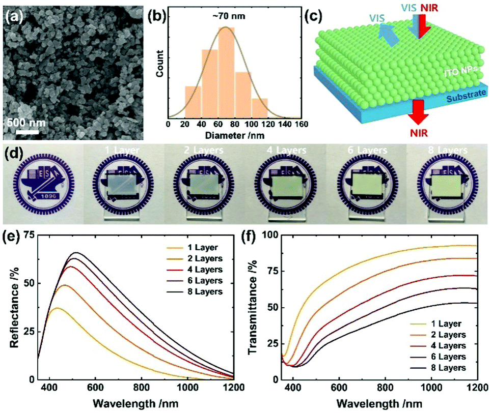 | ||
| Fig. 1 (a) SEM image and (b) size distribution of ITO nanoparticles in this research. (c) Illustration showing light-selective properties of an ITO nanoparticulate electrode, which is simplified from the data shown in (e and f). (d) Optical images of ITO electrodes showing decreasing visibility of the logo with increasing layers (i.e. thickness). (e) Light reflectance and (f) transmittance spectra depending on the thickness of the ITO electrodes. | ||
The optical properties systematically altered with the thickness of the ITO film. For example, a thick ITO film lost transparency of visible light manifested as a faded logo (Fig. 1d). This effect is a result of increased light reflection, as presented in Fig. 1e. Specifically, the thicker the ITO film (from 2.1 to 16.2 μm), the more enhanced the visible reflectance (37 to 66% at the maximum), concurrent with a shift to longer wavelength (from 434 to 516 nm) (see Table S1 (ESI†) in which characteristic values are listed). To understand these results, we performed an optical simulation (the corresponding results appear in Fig. S2a, ESI†) that shows large ITO NPs (diameter near 140 nm) to possess improved efficiency of reflection of visible light while shifting the reflection to a greater wavelength. As a thicker film contains more number of large ITO NPs, these simulation results account for the enhanced and shifted properties exhibited in Fig. 1e. In contrast, large reflectance of 16, 29, 42, 48 and 53% for 1, 2, 4, 6 and 8 layers at 650 nm, respectively, was demonstrated, implying light harvesting in the entire visible region. The striking difference of the ITO nanoparticulate electrodes from the classical electrodes such as Ag or Au is that the reflection co-exists with the near-infrared transmission (93, 84, 72, 63 and 53% at 1150 nm) that increases with the decreasing thickness of the film (Fig. 1c and f). Such light properties would be desirable for tandem applications such as PSC/PSC or PSC/photodetector for near-infrared sensing. It is likely from the simulation result in Fig. S2b (ESI†) that the bigger particles >∼200 nm would aggressively reflect the near-infrared light so as to eliminate the unique promising property.
We fabricated the mesoscopic PSC by sequentially screen-printing the mesoporous TiO2 (electron transport layer), Al2O3 (insulating layer) and ITO (HTM-free electrode) scaffolds and infiltrating the perovskite with drop-casting (further details in ESI†). In Fig. 2a, the final device is shown schematically, based on an image from the scanning electron microscope (SEM) to visualize the perovskite completely infiltrated into the TiO2/Al2O3 scaffolds, which is further supported with optical images in Fig. 2b. As schematically drawn in Fig. 2c, the infiltrated perovskite crystal is based on the hybrid cation41 of formamidinium (FA, 80%) and guanidinium (GA, 20%) with additive SnF2 (20%) and co-additive EDAI2 (15%) according to the optimal performance of the carbon devices; the results are shown in Fig. S3 and Table S2, ESI.† An incorporation of EDAI2 (0–20%) led to systematic alteration of the crystal structure and optical properties (Fig. S4, SEI) consistent with literature reports;26,53,54 the optimal EDAI2 (15%) decreased the Sn4+ defect states > five-fold (XPS spectra, Fig. S5a and b, ESI†). An energy-level diagram of the PSC sketched in Fig. 2d indicates the energetically aligned perovskite and ITO, where the perovskite energy levels including a band gap of 1.61 eV were obtained according to the results shown in Fig. S4a and S5c, d. It is worth noting that ITO is a degenerate n-type semiconductor but it can efficiently extract holes from the perovskites, evidenced by a quasi ohmic J–V behavior of the hole-only ITO device shown in Fig. 2e, via the formation of a recombination junction;55,56 the analogous interface is the ITO/PEDOT:PSS in the planar PSC. Meanwhile, despite pursuing scalable tin-based PSC herein, we have fabricated the mesoscopic ITO PSC with a lead perovskite (i.e., MAPbI3) to gain generality. The resulting power conversion efficiency (PCE) of 11.3% shown in Fig. 2f is comparable to that of the planar ITO PSC.57
 | ||
| Fig. 2 (a) Schematic drawing and cross-sectional SEM image of a mesoscopic PSC incorporating an ITO electrode on top. The SEM image was taken following optimization. (b) Optical images taken before and after perovskite deposition showing a darker black from the substrate side than from the ITO side because of excellent infiltration. (c) Illustration of lead-free tin-based perovskite: white parts represent Schottky vacancies. (d) Diagram of energy levels for selective electron and hole extractions in PSC. (e) Linear J–V curve of the hole-only device of ITO NP/Cu:NiO/FTO (inset: logarithmic J–V curve with symmetry). (f) Representative J–V curve of MAPbI3 ITO device measured under standard one-sun illumination. | ||
To confirm the effects of the light reflectance, we applied ITO films of 1, 2, 4, 6 and 8 layers corresponding to the thicknesses of 2.1, 4.2, 7.8, 11.0 and 14.3 μm, respectively. Characteristic J–V curves measured under one-sun illumination (AM 1.5G, 100 mW cm−2) are shown in Fig. 3a and Table S3 (ESI†). The best PCE (4.4%) resulted from four ITO layers. With increasing thickness of the ITO from 1 to 4 layers, the short-circuit current (JSC) and fill factor (FF) were enhanced from 15.1 to 16.7 mA cm−2 and 42.4 to 55.6%, respectively, while nearly maintaining an open-circuit voltage (VOC) of ∼0.48 V. As the cross-sectional SEM images (Fig. S6, ESI†) display an excellent infiltration of the perovskite into TiO2/Al2O3 for one and two ITO layers, their decreased FF is associated with the relatively high sheet resistances (Table S1, ESI†). The results of measurement of the spectra for the efficiency of conversion of the incident photons to current (IPCE) are shown in Fig. 3b: the integrated current densities from the IPCE match well with the JSC from the measurement of J–V. The IPCE spectra track enhanced responses in the range of 380–800 nm with much greater response over the wavelengths beyond 600 nm with increasing thickness of ITO (i.e. increasing light reflection), accounting for the increased JSC of the device with four ITO layers. Further increasing the thickness to 6 and 8 layers degraded all the photovoltaic performance. This effect is likely correlated with incomplete infiltration of the perovskite into the TiO2/Al2O3 layers, as shown in Fig. S6, ESI,† which impedes the light harvesting and charge collection to the TiO2.
 | ||
| Fig. 3 (a) Representative J–V curves measured under standard one-sun illumination and (b) IPCE spectra of ITO devices with varied layers. (c–f) Statistical histogram of 30 ITO devices each at non-optimal and optimal conditions; all photovoltaic parameters are improved concurrently with minimal spread following optimization. | ||
The performance of the best device with four ITO layers was further improved on increasing the concentration of the precursor solution from 1 to 1.5 M, according to the results shown in Fig. S7a and Table S4, ESI.† The PCE attained 5.1% at the perovskite concentration of 1.15 M where the complete infiltration of the perovskite into TiO2/Al2O3 was realized (see Fig. 2a and Fig. S6c, ESI†). The J–V curves taken from the forward and reverse scan direction at the optimal condition are presented in Fig. S7b, ESI,† which shows a minor effect of hysteresis. To compare statistically the optimal condition with the former condition, we show histograms of photovoltaic parameters with 30 devices in Fig. 3c–f; the corresponding parameters are listed in Tables S5 and S6, ESI.† The optimal condition raised all the photovoltaic parameters with a narrow distribution: VOC rose from 0.474 ± 0.022 to 0.491 ± 0.018 V; JSC rose from 16.1 ± 1.5 to 17.6 ± 0.8 mA cm−2; FF rose from 54.7 ± 3.0 to 54.9 ± 2.2%; PCE hence rose from 4.1 ± 0.4% to 4.7 ± 0.3%. Furthermore, the best ITO device attained a PCE of 5.4%, which is the greatest among all-solution-processed lead-free PSCs.19,20,22,23,58,59 The performance of the ITO device is also superior to those of the FA-based tin PSCs using Spiro-OMeTAD as the HTM (Table S7, ESI†). Note that the back-contact electrodes of these regular planar or mesoscopic devices were made by thermal evaporation of silver metal under high vacuum condition limiting their future industrial scalability. While the planar devices adopt ∼200 nm thickness, closely associated with the effective charge diffusion length, for high-performance tin perovskites in solar cells,14,15,27,28,32–34,41 the 1 μm thick Al2O3 insulating film in the mesoscopic devices is too harsh in terms of effective charge carrier diffusion for the tin perovskites. The further improvement in the PCE is likely made by decreasing the Al2O3 thickness.
Following the optimization, we compared the ITO device with the carbon device. The same experimental conditions except the ∼10 μm thick carbon layer optimized in our earlier researches20,23 was adopted for the carbon device. Even though carbon possesses a low sheet resistance of 26 ± 1 Ω sq.−1, the PCE of ITO is nearly twice that of carbon (PCE 5.4% for ITO vs. 3.0% for carbon), as shown in Fig. 4a (results summarized in Table S8, ESI†). In the IPCE spectra, Fig. 4b, the integrated JSC match the current densities of the J–V curves for both the devices. The ITO device attained IPCE responses over ∼80% for the wavelength range of 400–650 nm and avoided significantly depressed responses beyond 650 nm, an issue found in the mesoscopic tin PSC; the attained IPCE rivals that for the planar tin PSC, as shown in the IPCE evolution chart in Fig. 4c (details are summarized in Table S9, ESI†). From the measured dark J–V characteristic curves (Fig. 4d), we found a significantly decreased charge recombination and charge injection barrier for the ITO device, representing superior catalytic activity for the ITO device than the carbon device. The results of electrochemical impedance spectroscopy (EIS), shown in Fig. S8, ESI,† indicate a greater charge-recombination resistance for the ITO device than for the carbon device (Table S10, ESI†). The distinction in contact interface – the seamless contact of Al2O3/ITO compared to the partly disjointed contact of Al2O3/carbon creating the vacant spaces (i.e., no perovskite filled)20 – would be responsible for the recombination. Combined with the light reflectivity, the excellent interfacial properties account for the significantly greater device performance of the ITO than that of the carbon.
 | ||
| Fig. 4 Comparison of ITO and carbon devices. (a) J–V curves measured under standard one-sun conditions. (b) IPCE spectra. (c) Evolution of IPCE (at 650 nm) of the inverted (p-i-n), regular (n-i-p), carbon and ITO devices. (d) J–V curves measured under darkness. (e) Output current density measured under the standard one-sun conditions, at maximum power point and under ambient air. | ||
As carbon is a member of a highly stable class of materials explored in diverse applications,39,60,61 comparing ITO with carbon can offer deep insight into operational stability. We thus compared the ITO device with the carbon device under three conditions: (i) un-encapsulated devices under one-sun illumination at the maximum power point (Fig. 4e) (ii) encapsulated devices in darkness (Fig. S9a, ESI†) and (iii) encapsulated devices under one-sun illumination (Fig. S9b, ESI†). It is well known that the tin perovskites suffer from unwanted rapid oxidation of Sn2+ to Sn4+ by water and oxygen, and in the carbon or ITO devices, tin perovskites can meet oxygen and gaseous molecular water diffused through the mesoporous ITO or carbon. Under the first condition, ITO showed nearly no decay (96% retention) whereas carbon displayed a rapid decay (28% retention) within 60 s. It is reasonable to infer that ITO is able to better protect the tin perovskite against oxygen and water in large due to the seamless contact between ITO and Al2O3 minimizing the exposure of the perovskite to ambient condition unlike the carbon/Al2O3 contact.20 Under the second condition, >90% retention of the initial PCE was attained for ITO, better than for carbon (>70% retention) for an enduring period >1000 h. Under the third condition, both the devices displayed a slight decrease for an initial ∼500 s but the PCE of the ITO device gradually increased (to 107% retention) whereas that of the carbon device constantly attenuated (81% retention) for 2 h. The device degradation under these conditions might arise from an unavoidable minute amount of water or oxygen present even after encapsulation. Despite this, the ITO device greatly suppressed the degradation for long periods unlike the carbon device, representing excellent stability by protecting the tin perovskite. Regardless of the measurement conditions, all results are consistent, and indicate that the ITO device can offer greater stability than the carbon device.
Conclusions
In conclusion, we have developed solution-processable ITO nanoparticulate electrodes to replace carbon electrodes in mesoscopic hybrid tin-based PSCs. The ITO device showed distinctive improvements over the carbon device with respect to light reflection, hole selectivity, device performance and stability. Unlike carbon, ITO has increased visible light reflectance with increasing film thickness. As a result, a PCE of 5.4% (cf. 3.0% for carbon) was attained, which is a record efficiency for a lead-free all-solution-processed PSC. The ITO device also demonstrated operational stability under darkness and light-soaking conditions greater than that of carbon, demonstrating >90% retention of the initial output compared to 30–80% retention for carbon. These remarkable optical properties together with the superior device performance make the ITO device a promising candidate for future applications, such as indoor devices in dim light and tandem solar cells or tandem hybrids.Conflicts of interest
There are no conflicts to declare.Acknowledgements
Taiwan Ministry of Science and Technology (grant MOST 108-2119-M-009-004) and Centre for Emergent Functional Matter Science of National Chiao Tung University from The Featured Areas Research Centre Program within the framework of the Higher Education SPROUT Project by Taiwan Ministry of Education provided financial support of this research. National Synchrotron Radiation Research Centre, Hsinchu Science Park, Taiwan, provided beam time for measurements of UPS.References
- Certified Best Cell Efficiency from NREL, https://www.nrel.gov/pv/assets/pdfs/best-research-cell-efficiencies.20200406.pdf.
- A. Kojima, K. Teshima, Y. Shirai and T. Miyasaka, J. Am. Chem. Soc., 2009, 131, 6050–6051 CrossRef CAS.
- H.-S. Kim, C.-R. Lee, J.-H. Im, K.-B. Lee, T. Moehl, A. Marchioro, S.-J. Moon, R. Humphry-Baker, J.-H. Yum, J. E. Moser, M. Grätzel and N.-G. Park, Sci. Rep., 2012, 2, 591 CrossRef.
- M. M. Lee, J. Teuscher, T. Miyasaka, T. N. Murakami and H. J. Snaith, Science, 2012, 338, 643–647 CrossRef CAS.
- J.-P. Correa-Baena, M. Saliba, T. Buonassisi, M. Grätzel, A. Abate, W. Tress and A. Hagfeldt, Science, 2017, 358, 739–744 CrossRef CAS.
- M. Saliba, T. Matsui, J.-Y. Seo, K. Domanski, J.-P. Correa-Baena, M. K. Nazeeruddin, S. M. Zakeeruddin, W. Tress, A. Abate, A. Hagfeldt and M. Grätzel, Energy Environ. Sci., 2016, 9, 1989–1997 RSC.
- Y. Rong, Y. Hu, A. Mei, H. Tan, M. I. Saidaminov, S. Il Seok, M. D. McGehee, E. H. Sargent and H. Han, Science, 2018, 361, eaat8235 CrossRef.
- K. Yoshikawa, H. Kawasaki, W. Yoshida, T. Irie, K. Konishi, K. Nakano, T. Uto, D. Adachi, M. Kanematsu, H. Uzu and K. Yamamoto, Nat. Energy, 2017, 2, 17032 CrossRef CAS.
- W. Ke and M. G. Kanatzidis, Nat. Commun., 2019, 10, 965 CrossRef.
- D. B. Mitzi, C. D. Dimitrakopoulos and L. L. Kosbar, Chem. Mater., 2001, 13, 3728–3740 CrossRef CAS.
- A. Waleed, M. M. Tavakoli, L. Gu, Z. Wang, D. Zhang, A. Manikandan, Q. Zhang, R. Zhang, Y.-L. Chueh and Z. Fan, Nano Lett., 2017, 17, 523–530 CrossRef CAS.
- W.-L. Hong, Y.-C. Huang, C.-Y. Chang, Z.-C. Zhang, H.-R. Tsai, N.-Y. Chang and Y.-C. Chao, Adv. Mater., 2016, 28, 8029–8036 CrossRef CAS.
- G. Xing, M. H. Kumar, W. K. Chong, X. Liu, Y. Cai, H. Ding, M. Asta, M. Grätzel, S. Mhaisalkar, N. Mathews and T. C. Sum, Adv. Mater., 2016, 28, 8191–8196 CrossRef CAS.
- S. Shao, J. Liu, G. Portale, H.-H. Fang, G. R. Blake, G. H. ten Brink, L. J. A. Koster and M. A. Loi, Adv. Energy Mater., 2018, 8, 1702019 CrossRef.
- K. Nishimura, M. A. Kamarudin, D. Hirotani, K. Hamada, Q. Shen, S. Iikubo, T. Minemoto, K. Yoshino and S. Hayase, Nano Energy, 2020, 74, 104858 CrossRef CAS.
- Z. Zhao, F. Gu, Y. Li, W. Sun, S. Ye, H. Rao, Z. Liu, Z. Bian and C. Huang, Adv. Sci., 2017, 4, 1700204 CrossRef.
- H. Xu, Y. Jiang, T. He, S. Li, H. Wang, Y. Chen, M. Yuan and J. Chen, Adv. Funct. Mater., 2019, 29, 1807696 CrossRef CAS.
- P. Li, X. Liu, Y. Zhang, C. Liang, G. Chen, F. Li, M. Su, G. Xing, X. Tao and Y. Song, Angew. Chem., Int. Ed., 2020, 59, 6909–6914 CrossRef CAS.
- M. Chen, M.-G. Ju, M. Hu, Z. Dai, Y. Hu, Y. Rong, H. Han, X. C. Zeng, Y. Zhou and N. P. Padture, ACS Energy Lett., 2019, 4, 276–277 CrossRef CAS.
- C.-M. Tsai, Y.-P. Lin, M. K. Pola, S. Narra, E. Jokar, Y.-W. Yang and E. W.-G. Diau, ACS Energy Lett., 2018, 3, 2077–2085 CrossRef CAS.
- W. Li, J. Li, J. Li, J. Fan, Y. Mai and L. Wang, J. Mater. Chem. A, 2016, 4, 17104–17110 RSC.
- C. M. Tsai, N. Mohanta, C. Y. Wang, Y. P. Lin, Y. W. Yang, C. L. Wang, C. H. Hung and E. W. G. Diau, Angew. Chem., Int. Ed., 2017, 56, 13819–13823 CrossRef CAS.
- M. Rameez, E. Y.-R. Lin, P. Raghunath, S. Narra, D. Song, M.-C. Lin, C.-H. Hung and E. W.-G. Diau, ACS Appl. Mater. Interfaces, 2020, 12, 21739–21747 CrossRef CAS.
- M. H. Kumar, S. Dharani, W. L. Leong, P. P. Boix, R. R. Prabhakar, T. Baikie, C. Shi, H. Ding, R. Ramesh, M. Asta, M. Graetzel, S. G. Mhaisalkar and N. Mathews, Adv. Mater., 2014, 26, 7122–7127 CrossRef CAS.
- E. Jokar, C.-H. Chien, A. Fathi, M. Rameez, Y.-H. Chang and E. W.-G. Diau, Energy Environ. Sci., 2018, 11, 2353–2362 RSC.
- W. Ke, C. C. Stoumpos, M. Zhu, L. Mao, I. Spanopoulos, J. Liu, O. Y. Kontsevoi, M. Chen, D. Sarma, Y. Zhang, M. R. Wasielewski and M. G. Kanatzidis, Sci. Adv., 2017, 3, e1701293 CrossRef.
- T. Nakamura, S. Yakumaru, M. A. Truong, K. Kim, J. Liu, S. Hu, K. Otsuka, R. Hashimoto, R. Murdey, T. Sasamori, H. Do Kim, H. Ohkita, T. Handa, Y. Kanemitsu and A. Wakamiya, Nat. Commun., 2020, 11, 3008 CrossRef CAS.
- C. Wang, F. Gu, Z. Zhao, H. Rao, Y. Qiu, Z. Cai, G. Zhan, X. Li, B. Sun, X. Yu, B. Zhao, Z. Liu, Z. Bian and C. Huang, Adv. Mater., 2020, 32, 1907623 CrossRef CAS.
- Q. Tai, X. Guo, G. Tang, P. You, T.-W. Ng, D. Shen, J. Cao, C.-K. Liu, N. Wang, Y. Zhu, C.-S. Lee and F. Yan, Angew. Chem., Int. Ed., 2019, 58, 806–810 CrossRef CAS.
- X. Meng, J. Lin, X. Liu, X. He, Y. Wang, T. Noda, T. Wu, X. Yang and L. Han, Adv. Mater., 2019, 31, 1903721 CrossRef CAS.
- S. J. Lee, S. S. Shin, Y. C. Kim, D. Kim, T. K. Ahn, J. H. Noh, J. Seo and S. Il Seok, J. Am. Chem. Soc., 2016, 138, 3974–3977 CrossRef CAS.
- X. Liu, Y. Wang, T. Wu, X. He, X. Meng, J. Barbaud, H. Chen, H. Segawa, X. Yang and L. Han, Nat. Commun., 2020, 11, 2678 CrossRef CAS.
- F. Wang, X. Jiang, H. Chen, Y. Shang, H. Liu, J. Wei, W. Zhou, H. He, W. Liu and Z. Ning, Joule, 2018, 2, 2732–2743 CrossRef CAS.
- X. Jiang, F. Wang, Q. Wei, H. Li, Y. Shang, W. Zhou, C. Wang, P. Cheng, Q. Chen, L. Chen and Z. Ning, Nat. Commun., 2020, 11, 1245 CrossRef CAS.
- C. Liu, J. Tu, X. Hu, Z. Huang, X. Meng, J. Yang, X. Duan, L. Tan, Z. Li and Y. Chen, Adv. Funct. Mater., 2019, 29, 1808059 CrossRef.
- W. Ke, C. C. Stoumpos, J. L. Logsdon, M. R. Wasielewski, Y. Yan, G. Fang and M. G. Kanatzidis, J. Am. Chem. Soc., 2016, 138, 14998–15003 CrossRef CAS.
- X. Liu, Y. Wang, F. Xie, X. Yang and L. Han, ACS Energy Lett., 2018, 3, 1116–1121 CrossRef CAS.
- A. Mei, X. Li, L. Liu, Z. Ku, T. Liu, Y. Rong, M. Xu, M. Hu, J. Chen, Y. Yang, M. Grätzel and H. Han, Science, 2014, 345, 295–298 CrossRef CAS.
- H. Chen and S. Yang, Adv. Mater., 2017, 29, 1603994 CrossRef.
- L. Qiu, S. He, L. K. Ono, S. Liu and Y. Qi, ACS Energy Lett., 2019, 4, 2147–2167 CrossRef CAS.
- E. Jokar, C.-H. Chien, C.-M. Tsai, A. Fathi and E. W.-G. Diau, Adv. Mater., 2019, 31, 1804835 CrossRef.
- Y. Zhang, S.-W. Ng, X. Lu and Z. Zheng, Chem. Rev., 2020, 120, 2049–2122 CrossRef CAS.
- H. C. Hulst and H. C. van de Hulst, Light scattering by small particles, Courier Corporation, 1981 Search PubMed.
- Q. Zhang, D. Myers, J. Lan, S. A. Jenekhe and G. Cao, Phys. Chem. Chem. Phys., 2012, 14, 14982–14998 RSC.
- R. Prasanna, T. Leijtens, S. P. Dunfield, J. A. Raiford, E. J. Wolf, S. A. Swifter, J. Werner, G. E. Eperon, C. de Paula, A. F. Palmstrom, C. C. Boyd, M. F. A. M. van Hest, S. F. Bent, G. Teeter, J. J. Berry and M. D. McGehee, Nat. Energy, 2019, 4, 939–947 CrossRef CAS.
- K. P. Marshall, M. Walker, R. I. Walton and R. A. Hatton, Nat. Energy, 2016, 1, 16178 CrossRef CAS.
- S. Ghanizadeh, T. A. N. Peiris, D. S. Y. Jayathilake, D. A. Hutt, K. G. U. Wijayantha, D. J. Southee, P. P. Conway, P. Marchand, J. A. Darr, I. P. Parkin and C. J. Carmalt, Ceram. Int., 2016, 42, 18296–18302 CrossRef CAS.
- Z. Song, S. C. Watthage, A. B. Phillips and M. J. Heben, J. Photonics Energy, 2016, 6, 1–23 Search PubMed.
- W. Gao, C. Chen, C. Ran, H. Zheng, H. Dong, Y. Xia, Y. Chen and W. Huang, Adv. Funct. Mater., 2020, 30, 2000794 CrossRef CAS.
- J. Lee, S. Lee, G. Li, M. A. Petruska, D. C. Paine and S. Sun, J. Am. Chem. Soc., 2012, 134, 13410–13414 CrossRef CAS.
- Z. Chen, W. Li, R. Li, Y. Zhang, G. Xu and H. Cheng, Langmuir, 2013, 29, 13836–13842 CrossRef CAS.
- G. Bühler, D. Thölmann and C. Feldmann, Adv. Mater., 2007, 19, 2224–2227 CrossRef.
- W. Ke, P. Priyanka, S. Vegiraju, C. C. Stoumpos, I. Spanopoulos, C. M. M. Soe, T. J. Marks, M.-C. Chen and M. G. Kanatzidis, J. Am. Chem. Soc., 2018, 140, 388–393 CrossRef CAS.
- S. Vegiraju, W. Ke, P. Priyanka, J.-S. Ni, Y.-C. Wu, I. Spanopoulos, S. L. Yau, T. J. Marks, M.-C. Chen and M. G. Kanatzidis, Adv. Funct. Mater., 2019, 29, 1905393 CrossRef CAS.
- M. De Bastiani, A. S. Subbiah, E. Aydin, F. H. Isikgor, T. G. Allen and S. De Wolf, Mater. Horiz., 2020, 7, 2791–2809 RSC.
- J. Meyer, S. Hamwi, M. Kröger, W. Kowalsky, T. Riedl and A. Kahn, Adv. Mater., 2012, 24, 5408–5427 CrossRef CAS.
- Z. Zhou and S. Pang, J. Mater. Chem. A, 2020, 8, 503–512 RSC.
- J. Shin, M. Kim, S. Jung, C. S. Kim, J. Park, A. Song, K.-B. Chung, S.-H. Jin, J. H. Lee and M. Song, Nano Res., 2018, 11, 6283–6293 CrossRef CAS.
- T. Zhang, H. Li, H. Ban, Q. Sun, Y. Shen and M. Wang, J. Mater. Chem. A, 2020, 8, 4118–4124 RSC.
- K. Fu, Y. Yao, J. Dai and L. Hu, Adv. Mater., 2017, 29, 1603486 CrossRef.
- L. Fagiolari and F. Bella, Energy Environ. Sci., 2019, 12, 3437–3472 RSC.
Footnote |
| † Electronic supplementary information (ESI) available. See DOI: 10.1039/d0ma00860e |
| This journal is © The Royal Society of Chemistry 2021 |