
 Open Access Article
 This Open Access Article is licensed under a
 Creative Commons Attribution 3.0 Unported Licence
Atomic scale surface modification of TiO2 3D nano-arrays: plasma enhanced atomic layer deposition of NiO for photocatalysis†
Jerome W. F.
Innocent
a,
Mari
Napari‡
 b,
Andrew L.
Johnson
*a,
Thom R.
Harris-Lee
a,
Miriam
Regue
c,
Timo
Sajavaara
d,
Judith L.
MacManus-Driscoll
b,
Frank
Marken
a and
Feras
Alkhalil
e
b,
Andrew L.
Johnson
*a,
Thom R.
Harris-Lee
a,
Miriam
Regue
c,
Timo
Sajavaara
d,
Judith L.
MacManus-Driscoll
b,
Frank
Marken
a and
Feras
Alkhalil
e
aDepartment of Chemistry, University of Bath, Claverton Down, Bath, BA2 7AY, UK. E-mail: chsalj@bath.ac.uk
bDepartment of Materials Science and Metallurgy, University of Cambridge, Cambridge, CB3 0FS, UK
cDepartment of Chemical Engineering, Imperial College London, London, SW7 2AZ, UK
dDepartment of Physics, University of Jyväskylä, FI-40014 Jyväskylä, Finland
ePragmatIC Printing LLC, Cambridge Science Park, Cambridge, CB4 0WH, UK
First published on 12th October 2020
Abstract
Here we report the development of a new scalable and transferable plasma assisted atomic layer deposition (PEALD) process for the production of uniform, conformal and pinhole free NiO with sub-nanometre control on a commercial ALD reactor. In this work we use the readily available nickel precursor nickelocene in conjunction with O2 plasma as a co-reagent (100 W) over a temperature range of 75–325 °C. An optimised growth per cycle of 0.036 nm was obtained at 250 °C with uniform thickness and coverage on scale-up to and including an 6 inch Si wafer (with a 200 nm thermal SiO2 top layer). The bulk characteristics of the NiO thin films were comprehensively interrogated by PXRD, Raman spectroscopy, UV-vis spectroscopy and XPS. The new NiO process was subsequently used to fabricate a 3D nanostructured NiO/TiO2/FTO heterojunction by depositing 20 nm of NiO onto pre-fashioned TiO2 nanorods at 250 °C for application in the photo-electrolysis of water in a photoelectrochemical cell (PEC). The NiO/TiO2 3D array was shown to possess a peak current of 0.38 mA cm−2 at 1.23 VRHE when stimulated with a one sun lamp.
1 Introduction
Nickel oxide (NiO) is a binary transition metal oxide material that has attracted considerable attention of late due to its chemical stability and electronic, magnetic and optical properties.1,2 Nickel-deficient NiO films exhibit wide band-gap (3.4–4.0 eV) p-type semiconducting behaviour, and are suited to application in resistive switching, random access memory (ReRAM) and in complementary metal oxide semiconductor (CMOS) technologies.3–5 For application it is of importance to develop controlled, conformal and reproducible NiO ALD processes for further device research and industrial application. For advanced electronics, atomic layer deposition (ALD) is regarded as a leading manufacturing technique.6,7Recently NiO has becoming increasingly prevalent in sustainable energy materials including solar cells and photocatalytic water splitting devices. NiO can be used as a hole collecting layer in photo junctions and has been shown to significantly improve the photocatalytic activity of materials such as perovskites.8–10 Alternatively, when utilised as a co-catalytic layer on TiO2 photoanodes, NiO has been shown to reduce the onset potential and increase the photoconversion efficiency.11 It has been proposed that the improvement in the photoanodes is a result of the formation of a P–N junction, which increases the charge separation and carrier lifetimes of TiO2.12 TiO2 can be grown in complex 3D structures, which can also improve the photoconversion efficiency of devices.13 ALD is an ideal tool for the growth of a co-catalytic layer as it can preserve the TiO2 geometry and the catalytic loading can be minimised by limiting the number of ALD cycles.
The ALD of NiO has been known for some time; the original studies by Utriainen et al. explored the use of a range of oxidation sources including water (H2O) and ozone (O3) with the nickel precursors [Ni(apo)2], [Ni(acac)2] and [Ni(dmg)2].14 It was proposed that reactive O3 was required for crystalline ALD growth with analogous studies using H2O as a co-reagent yielding amorphous materials. Limited precursor reactivity was believed to prevent crystalline NiO growth with H2O. However, improvements in precursor reactivity have since enabled low temperature crystalline growth of NiO with H2O as a co-reagent.15–17 Despite progress, the processes remain hindered by thermally unstable precursors which require long pulse and purge times and display limited growth rates. Furthermore, it has since been shown that NiO can catalytically decompose O3, which can limit homogeneous ALD growth, making it an unsuitable co-reagent for the ALD of NiO, especially on a large scale.18
To overcome the limitations of the thermal ALD of NiO, plasma enhanced ALD (PEALD) using highly reactive oxygen (O2) plasma can be utilised. The strongly oxidising plasma facilitates ALD reactions for precursors which are volatile but lack the required chemical reactivity for thermal ALD, such as nickel metallocenes and acetylacetonates.19 To the best of our knowledge, only four studies have been completed using cyclopentadienyl based systems, specifically nickelocene, [Ni{η5-C5H5}2] (Ni(Cp)2), methyl-nickelocene, [Ni{η5-C5H4Me}2] (Ni(MeCp)2), and ethyl-nickelocene, [Ni{η5-C5H4Et}2] (Ni(EtCp)2), with oxygen plasma.9,20–22
These studies have demonstrated that conformal growth of NiO is possible with cyclopentadienyl based nickel precursors and O2 plasma. Given the low cost of nickelocene (Ni(Cp)2), it should be an attractive precursor for ALD. However, the published processes utilising Ni(Cp)2 exhibit both prohibitively long deposition times and slow growth rates (0.011–0.012 nm per cycle), alongside high carbon content (ca. 12%) within the deposited films.22
Here we present a direct-plasma method for the deposition of NiO using the precursor Ni(Cp)2, and O2 plasma. The process was utilised in a new fabrication process for 3D nanostructured arrays, for application in photoelectrochemical water splitting. A systematic investigation has determined that the process is highly efficient and produced uniform and reproducible NiO with low carbon content. The film stoichiometry, roughness and crystallinity have all been investigated as a function of deposition temperature between 75 °C and 325 °C. The optimised process was used to grow 20 nm (600 PEALD cycles) of NiO on solvo-thermally grown TiO2 nanorods and the film uniformity, coverage and effectiveness as a photoelectrochemical co-catalyst were assessed.
2 Experimental
All depositions were performed on a Beneq TFS-200 reactor using a direct capacitively-coupled plasma configuration. Nickelocene, Ni(Cp)2, 99%, was purchased from STREM Chemicals and used without further purification. Ni(Cp)2 was kept in a HS300 stainless steel container and heated to 60 °C. To avoid condensation of the precursor, nitrogen (N2) was used as a carrier gas and as a purging gas. O2 and N2 were used in the plasma system and maintained at 50 sccm and 200 sccm, respectively, throughout the deposition (Fig. 1).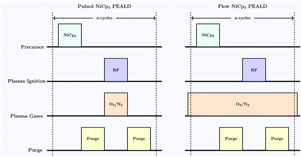 | ||
| Fig. 1 Schematic of the flow and pulsed PEALD process tested for the deposition of NiO. | ||
A 13.56 MHz RF power source (CESAR 133, Advanced Energy) and impedance matching network (Navio, Advanced Energy) system was used to generate O2 plasma. The process was systematically examined to optimise the precursor pulse and purging times. During deposition a plasma power of 100 W was applied and depositions were completed in a temperature range of 75–325 °C.
The film thickness was measured using spectroscopic ellipsometry (Stokes LSE-USB ellipsometer). X-ray diffraction (XRD) and X-ray reflectivity (XRR) measurements were used to determine the film density using a Bruker D8 X-ray diffractomer with CuK incident X-rays. The crystallinity was measured using powder X-ray diffraction (XRD) (Bruker D8 XRD system). Time-of-flight elastic recoil detection analysis (ToF-ERDA) was used to discover the elemental compositions of the films. A 13.6 MeV 79Br7+ ion beam was used to measure the film composition and the data was analysed with Potku analysis software. Further elemental analysis was performed with an Escalab 250XI (Thermo Fischer Scientific) microprobe was used for X-ray photoelectron spectroscopy (XPS) measurements. Raman spectra were collected using a Renishaw “inVia” confocal microscope, with a 325 nm UV laser in the backscattering configuration. The surface roughness was estimated using atomic force microscopy (AFM) (Nanoscope IIIA microscope). The root-mean-squared (RMS) roughness values were calculated using 2 × 2 μm areas. The band gaps of the NiO films grown on borosilicate glass (0.7 mm thick) were measured using ultraviolet-visible spectroscopy (Perkin Elmer “Lambda 750” UV/VIS/NIR Spectrophotometer).
The TiO2 nano-rods were grown solvo-thermally using the method reported by Zhang et al.23 on fluorine doped tin oxide (FTO, AGC type U TCO glass) coated glass and were subsequently coated with approximately 20 nm of NiO at 250 °C using 600 cycles of the saturation optimised PEALD method.23 Scanning electron microscopy was used to assess the film uniformity (JEOL JSM-6301F FESEM) and the growth of NiO was confirmed using X-ray analysis (Oxford INCA X-ray analyser).
3 Results and discussion
Initial investigations focused on establishing an optimised process for the deposition of NiO with films grown on silicon wafers with approximately 200 nm of thermal silicon dioxide (SiO2). Fig. 2a and b show the growth rate dependencies with respect to the precursor pulse length and plasma ignition time. The reactor temperature was fixed at 250 °C, and mass flow controllers delivered 50 sccm of O2 and 200 sccm of diluting N2. 100 W was applied for plasma ignition and both N2 purges were 5 s. Initial studies used a continuous flow of O2 with a 4 s plasma ignition pulse followed by an 8 s Ni(Cp)2 pulse. The Ni(Cp)2 pulse was reduced to 1 s before a reduction in growth rate was observed and similarly a 1 s plasma pulse is necessary to fully saturate the substrate surface. No deposition was observed after the performance of control experiments utilising a continuous flow of O2 (50 sccm) without plasma ignition in the presence of Ni(Cp)2. This precludes the possibility of a CVD reaction between Ni(Cp)2 and molecular O2 at 250 °C. As part of this study an alternative NiO ALD procedure with sequential O2 delivery pulses was investigated. It was determined that the film composition and structure for both the flow and pulsed PEALD procedures are equivalent. Longer purge times of 10 s were investigated and were shown not to affect the NiO growth rate, suggesting that purge times of 5 s are sufficient for removing all reaction by-products and excess Ni(Cp)2 precursor (Fig. 3).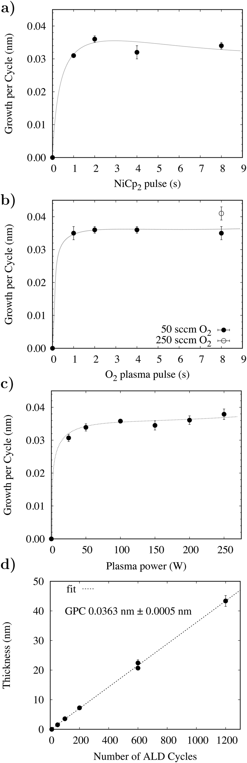 | ||
| Fig. 2 Optimisation of the Ni(Cp)2 PEALD process, all depositions completed at 250 °C. (a) Growth rate with respect to the Ni(Cp)2 delivery pulse. (b) Growth rate vs. O2 plasma pulse. (c) Growth rate as a function of plasma power. (d) Linearity of growth rate of NiO with respect to the number of ALD cycles. | ||
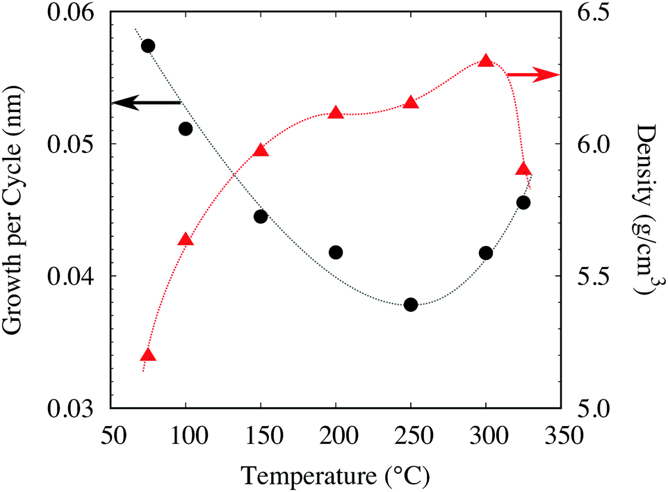 | ||
| Fig. 3 Variation of the growth rate and film density with the deposition temperature. All depositions utilised the optimised method (2 s/5 s/2 s/5 s) with 100 W plasma power. | ||
Fig. 2c shows the results of a series of depositions performed at 250 °C with a variation in the RF pulse from 50–250 W. A minimum of 50 W is necessary to achieve the optimum growth rate of 0.036 nm per cycle and, as shown in Fig. 4c, the plasma power did not affect the film roughness, with highly uniform films grown throughout the entire plasma range. Using a 100 W RF pulse at 250 °C in combination with the optimised pulse sequence the process has demonstrated excellent uniformity of NiO on 6′′ silicon wafers as shown in Fig. S1 (ESI†). The 6′′ wafer was coated evenly and without pinholes, demonstrating that the growth has been optimised and the PEALD method is scalable to large area device processing. The film growth rate was investigated between 75 and 325 °C. The growth rate was found to reduce from 0.06 nm per cycle at 75 °C to 0.036 nm per cycle at 250 °C before increasing to 0.048 nm per cycle at 325 °C. Consistent growth rates can typically be achieved with many ALD processes within a range referred to as the thermal window. No such behaviour was noted in this process. A report by Koushik et al. noted similar thermal behaviour for a Ni(MeCP)2 PEALD process and suggested that the behaviour was a consequence of a change in density.9 To affirm this, the film density between 75 and 325 °C was investigated by XRR. XRR measurements determined that between 75 and 200 °C the film density increased from 5.1–6.2 g cm−3 and reduced to 5.8 g cm−3 at 325 °C. It is therefore likely that the film growth rate reduces as a function of temperature due to a densification of the films. We propose that the increase in density of the films between 200 and 300 °C is a result of increased film crystallinity (see Fig. S2, ESI†) and the subsequent reduction in density at 325 °C is a consequence of increased carbon impurities incorporated by the thermal decomposition of Ni(Cp)2. From the XRR measurements and film growth rates it has been determined that the optimal growth window for NiO using Ni(Cp)2 and O2 plasma lies between 200 and 300 °C.
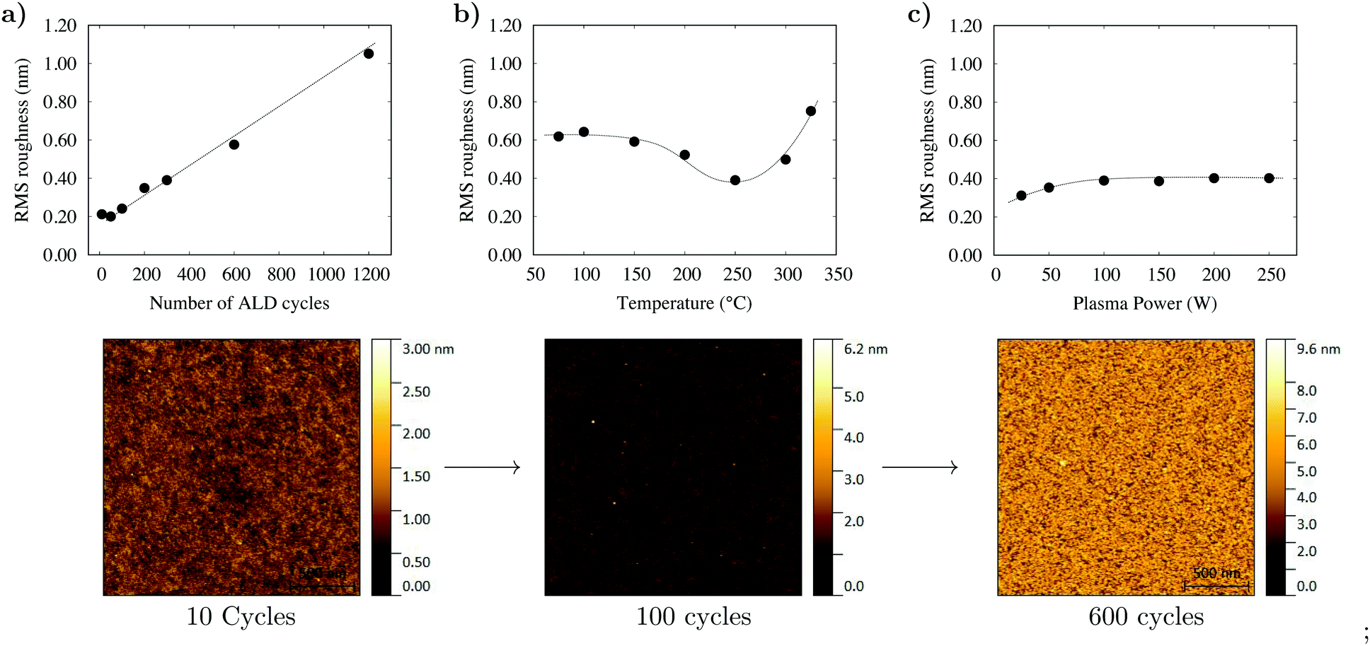 | ||
| Fig. 4 PEALD depositions performed with a sequence of 2 s/5 s/2 s/5 s. Changes in the film roughness with respect to (a) the number of ALD cycles and (b) the deposition temperature between 75 and 325 °C, and (c) NiO grown at 250 °C with the plasma power varied from 50–300 W. | ||
The linearity of the growth rate was investigated at 250 °C using the optimised pulse sequence of 2 s/5 s/2 s/5 s. Fig. 2d shows how the growth rate remains constant between 10 and 1200 PEALD cycles. As the number of PEALD cycles is increased the thickness of NiO increases linearly at a growth rate of 0.036 nm per cycle. The process provided precise control over the film thickness with only a short nucleation delay over the first 10 cycles. Previous literature has shown that discerning the precise stoichiometry of NiO thin films using XPS is challenging.24 Following literature precedent, a basic fitting of the XPS spectra was completed (see Fig. S3, ESI†) and charge corrected to C1s = 248.8 eV with signature Ni 2p3/2 and O1s peaks at 853.82 eV and 529.43 eV, respectively. The measurements were in good agreement with the ToF-ERDA and XPS, showing that the films are nonstoichiometric with Ni![[thin space (1/6-em)]](https://www.rsc.org/images/entities/char_2009.gif) :O = 0.71.
:O = 0.71.
Fig. 5 shows the room temperature Raman scattering of a 100 nm NiO sample oriented in the (200) plane. The first-order transverse optical (TO) and longitudinal optical (LO) phonons and second-order (2TO and 2LO) phonons observed are consistent with those in the literature.25,26 The TO and LO modes are inactive in rock-salt crystals unless there are defects within the lattice. The intense LO and TO phonons observed in this sample suggest there are significant defects within the lattice. The Ni:O ratio of 0.71 suggests that the LO and TO intensity is a result of metal vacancies within the lattice.25
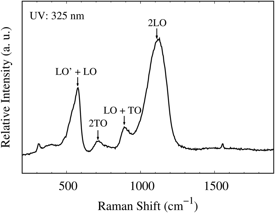 | ||
| Fig. 5 The room-temperature backscattering Raman spectra from a 325 nm excitation source. LO′ + LO (430–635 cm−1), 2TO (720 cm−1), LO + TO (850–940 cm−1) and 2LO (1120 cm−1). | ||
The surface morphology of the as-deposited films was measured as a function of the film thickness, deposition temperature and plasma power as shown in Fig. 4. A 2 × 2 μm area was measured by AFM and the root mean square (RMS) roughness calculated. All of the deposited films were found to be highly uniform, with the smoothest film deposited at 250 °C with an RMS of 0.4 nm. Typical for ALD growth of polycrystalline films, the film roughness increased linearly with respect to the film thickness as shown in Fig. 4b. UV-vis spectroscopy was used to measure the band gap of a 100 nm NiO film. The film had a bandgap of 3.62 eV, which falls within the expected range for NiO (see Fig. S4, ESI†).27,28 The electrical properties of the films were characterised by Hall effect measurements. The resistivity of a 100 nm sample of NiO on borosilicate glass was 1.31 × 10⁴ Ω cm and it was confirmed to have p-type conductivity with holes as majority carriers. The hole density was 2.5 × 1015 cm−3 and the mobility 0.2 cm2 V s−1.
Using the optimised deposition procedure approximately 20 nm of NiO was deposited onto rutile TiO2 nanorods with 600 PEALD cycles at 250 °C. Incorporation of NiO was confirmed by SEM-EDX with 18.5 wt% Ni detected (see Fig. S6, ESI†). The NiO film coverage was assessed by comparing FE-SEM images of the TiO2 and TiO2–NiO nanorods; show in Fig. 6 are the TiO2 nanorods before and after coating with 20 nm of NiO. The TiO2–NiO nanorods display thickening toward the top, with a continuous film formed between densely packed clusters of nanorods. The growth gradient from the nanorod peak to the base is consistent with a process that is recombination limited and suggests that oxygen radical species recombine faster than deposition can occur in high aspect ratio environments.29
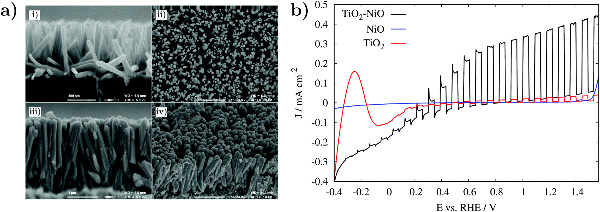 | ||
| Fig. 6 (a) FE-SEM images of TiO2 nanorods and TiO2 nanorods coated with 600 Ni(Cp)2 PEALD cycles. (i) and (ii) show the TiO2 nanorods and (iii) and (iv) show the nanorods after coating with 20 nm of NiO. (b) j–V curves measured in 1 M KOH (pH = 13.6) of pristine TiO2, pristine NiO and TiO2–NiO samples. All measurements were performed under 1 sun chopped (AM 1.5G, 100 mW cm−2) back-side illumination. | ||
The TiO2 nanorods are predominantly orientated perpendicular to the substrate in the (101) plane. Due to the nature of the nanorods, AFM could not be used to estimate the surface roughness; however, visually from the FE-SEM we can suggest that the aspect ratio varies significantly across the surface and each nanorod is estimated to have an aspect ratio between 9 and 17. The 600 cycle NiO PEALD coating (estimated to be 20 nm according to Fig. 2d) was not suitable for maintaining complete nanorod uniformity and the substrate surface area has been significantly reduced. However, the large spatial voids between TiO2–NiO clusters maintain a relatively high surface area and are suitable active sites for photochemical water splitting and may still enhance the overall photoelectrochemical (PEC) performance of the TiO2 nanorods.
TiO2 nanorods with and without the NiO coating were tested in a PEC cell to evaluate the effect of NiO loading on the PEC performance. Fig. 6 shows J–V curves of pristine TiO2 nanorods, pristine NiO and TiO2–NiO samples measured under back-side illumination. The pristine TiO2 nanorods exhibited the lowest PEC performance of 0.03 mA cm−2 at 1.23 VRHE under simulated solar light, whereas no photocurrent response was detected for the pristine NiO control sample. Incorporation of a 20 nm layer of NiO on top of TiO2 remarkably improved the PEC performance by a factor of 12, achieving a value of ca. 0.38 mA cm−2 at 1.23 VRHE. In fact, a significant improvement in the PEC performance was achieved in all the potential window range studied. A smaller onset potential was observed in the TiO2–NiO samples in comparison with pristine TiO2, as expected.11 At low bias (0 to 0.5 VRHE), large anodic photocurrent transients appeared in the TiO2–NiO samples, indicating trapping of photogenerated holes at the electrode–electrolyte interface. This is a common feature also observed in other TiO2 systems loaded with different co-catalysts.30,31 At larger bias, these photocurrent transients disappeared and efficient charge transfer occurred. On balance, incorporation of a 20 nm layer of NiO on top of TiO2 is demonstrated to be an effective approach to successfully improve the PEC performance of TiO2 nanorods.
Conventionally, PEALD is considered to be hindered by conformity issues and its directional nature makes it less suited to 3D structures. This preliminary study has demonstrated that the NiO PEALD method utilised in this study, despite not being optimised for 3D substrates, was an effective method for the deposition of a co-catalytic layer which maintained minor 3D substrate features. Currently under investigation are the effects of adjusting the PEALD deposition sequence in order to improve the 3D substrate coverage. By systematically altering the precursor and plasma pulse lengths we aim to compensate for the diffusion limitations of high aspect ratio substrates and improve the 3D coverage of the NiO PEALD process.32
It has previously been demonstrated in the literature that the addition of NiO to TiO2 and the subsequent formation of a p–n junction prolongs photogenerated hole–electron lifetimes and increases the PEC performance.11,33–35 As noted earlier, many factors such as the film thickness, crystallinity, and phase matching at grain boundaries will all have a profound effect on the photocatalytic performance. However, the most significant factor by far is the p-type conductivity of NiO. In its stoichiometric form NiO is an insulator but it can express p-type conductivity if a sufficient amount of Ni3+ states are introduced. Typically this can be done via doping (e.g. with Li) or by creating Ni vacancies by increasing the oxygen concentration in the films (vide supra).19
We are confident however that with respect to the process that we report here, of the possible variables which will impact the p-type behaviour and stoichiometry (e.g. pulse lengths, plasma power etc.), the temperature at which deposition occurs is by far the most critical: high enough to enable complete surface reactions but low enough to prevent precursor decomposition and contamination. Continued studies are focusing on the optimisation of both physical and chemical parameters in the TiO2–NiO PEC.36,37
4 Conclusions
In this study a Ni(Cp)2 PEALD method which utilises direct plasma ignition has been systematically investigated. From iterative adjustment of the precursor delivery, plasma pulse length and plasma power, the overall process was optimised to a 2 s/5 s/2 s/5 s Ni(Cp)2 and O2 PEALD cycle, which utilised a 100 W RF pulse. In the range of 150–300 °C, NiO was deposited with a density greater than 6.0 g cm−3 and at a growth rate ranging from 0.034–0.048 nm per cycle. Samples prepared at 250 °C were determined to be oxygen rich with an Ni:O ratio of 0.71 with negligible carbon contamination. The process has demonstrated that direct plasma ignition is an effective means of growing NiO as it requires only short cycle times to facilitate uniform NiO growth which can be scaled to an 6′′ wafer. The process has excellent growth linearity and can controllably grow NiO films up to 100 nm in thickness (see Fig. S7, ESI†).
To assess the deposition uniformity on complex substrates, approximately 20 nm of NiO was coated onto TiO2 nanorods. The nanorods, though not entirely homogeneous, were shown to maintain their high surface area with large spatial voids pocketed throughout the surface. The TiO2–NiO samples were shown to have an improved photoanodic response when stimulated by a one sun lamp after coating with NiO with a peak current of 0.38 mA cm−2 at 1.23 VRHE. We conclude that a NiO PEALD deposition method can be suitable for the growth of photoanodic co-catalysts on complex substrate geometries.
It should, however, be clearly noted that while we have worked towards the optimisation of a plasma enhanced ALD process for the fabrication of conformal NiO thin films, optimization of the photoanodic properties of the TiO2–NiO PEC is ongoing.
Conflicts of interest
There are no conflicts to declare.Acknowledgements
The authors would like to thank PragmatIC Printing PLC (https://www.pragmatic.tech/) for funding. A. L. J. acknowledges financial support from the University of Bath and PragmatIC Printing PLC (PhD studentship to J. W. F. I), and the Department of Chemistry, University of Bath (MChem Studentship to T. R. H.-L.). J. L. M.-D. and M. N. acknowledge financial support from the E.P.S.R.C (EP/P027032/1) and the University of Cambridge. J. L. M.-D. also acknowledges the Royal Academy of Engineering under the Research Chair scheme (No.: CieT1819\24).Notes and references
- F. Shan, A. Liu, H. Zhu, W. Kong, J. Liu, B. Shin, E. Fortunato, R. Martins and G. Liu, J. Mater. Chem. C, 2016, 4, 9438–9444 RSC.
- K. Sajilal and A. M. Ezhil Raj, Mater. Lett., 2016, 164, 547–550 CrossRef CAS.
- D.-Y. Cho, S. J. Song, U. K. Kim, K. M. Kim, H.-K. Lee and C. S. Hwang, J. Mater. Chem. C, 2013, 1, 4334 RSC.
- A. Lamperti, S. Spiga, H. L. Lu, C. Wiemer, M. Perego, E. Cianci, M. Alia and M. Fanciulli, Microelectron. Eng., 2008, 85, 2425–2429 CrossRef CAS.
- H. Shima, F. Takano, H. Akinaga, Y. Tamai, I. H. Inoue and H. Takagi, Appl. Phys. Lett., 2007, 91, 012901 CrossRef.
- R. W. Johnson, A. Hultqvist and S. F. Bent, Mater. Today, 2014, 17, 236–246 CrossRef CAS.
- X. Meng, X. Wang, D. Geng, C. Ozgit-Akgun, N. Schneider and J. W. Elam, Mater. Horiz., 2017, 4, 133–154 RSC.
- S. Seo, I. J. Park, M. Kim, S. Lee, C. Bae, H. S. Jung, N. Park, J. Y. Kim and H. Shin, Nanoscale, 2016, 8, 11403–11412 RSC.
- D. Koushik, M. Jošt, A. Dučinskas, C. Burgess, V. Zardetto, C. Weijtens, M. A. Verheijen, W. M. M. Kessels, S. Albrecht and M. Creatore, J. Mater. Chem. C, 2019, 7, 12532–12543 RSC.
- Z. Liu, A. Zhu, F. Cai, L. Tao, Y. Zhou, Z. Zhao, Q. Chen, Y.-B. Cheng and H. Zhou, J. Mater. Chem. A, 2017, 5, 6597–6605 RSC.
- M. A. Rasheed, R. Rahimullah, S. K. Uddin, N. Khaliq, Y. Khan, A. Waheed, A. Shah, A. Mahmood and G. Ali, Appl. Nanosci., 2019, 9, 1731–1742 CrossRef CAS.
- S. A. Rawool, M. R. Pai, A. M. Banerjee, A. Arya, R. Ningthoujam, R. Tewari, R. Rao, B. Chalke, P. Ayyub, A. Tripathi and S. R. Bharadwaj, Appl. Catal., B, 2018, 221, 443–458 CrossRef CAS.
- M. Gao, L. Zhu, W. Ong, J. Wang and G. W. Ho, Catal. Sci. Technol., 2015, 5, 4703–4726 RSC.
- M. Utriainen, M. Kröger-Laukkanen and L. Niinistö, Mater. Sci. Eng., B, 1998, 54, 98–103 CrossRef.
- T. S. Yang, W. Cho, M. Kim, K. S. An, T. M. Chung, C. G. Kim and Y. Kim, J. Vac. Sci. Technol., A, 2005, 23, 1238–1243 CrossRef CAS.
- C. Hsu, H. Su, C. Hou, J. Shyue and F. Tsai, Nanotechnology, 2015, 26, 385201 CrossRef.
- E. Lindahl, M. Ottosson and J. O. Carlsson, Chem. Vap. Deposition, 2009, 15, 186–191 CrossRef CAS.
- M. Stoyanova, P. Konova, P. Nikolov, A. Naydenov, S. Christoskova and D. Mehandjiev, Chem. Eng. J., 2006, 122, 41–46 CrossRef CAS.
- M. Napari, T. N. Huq, T. Maity, D. Gomersall, K. M. Niang, A. Barthel, J. E. Thompson, S. Kinnunen, K. Arstila, T. Sajavaara, R. L. Z. Hoye, A. J. Flewitt and J. L. MacManus-Driscoll, InfoMat, 2020, 2(4), 769–774, DOI:10.1002/inf2.12076.
- S. Ji, W. Jang, J. Son and D. Kim, Korean J. Chem. Eng., 2018, 35, 2474–2479 CrossRef CAS.
- A. G. Hufnagel, A. K. Henß, R. Hoffmann, O. E. O. Zeman, S. Häringer, D. Fattakhova-Rohlfing and T. Bein, Adv. Mater. Interfaces, 2018, 5, 1701531 CrossRef.
- Y. Koshtyal, D. Nazarov, I. Ezhov, I. Mitrofanov, A. Kim, A. Rymyantsev, O. Lyutakov, A. Popovich and M. Maximov, Coatings, 2019, 9, 301 CrossRef CAS.
- G. Zhang, X. Zhang, H. Huang, J. Wang, Q. Li, L. Q. Chen and Q. Wang, Adv. Mater., 2016, 4811–4816 CrossRef CAS.
- M. C. Biesinger, B. P. Payne, L. W. M. Lau, A. Gerson and R. S. C. Smart, Surf. Interface Anal., 2009, 41, 324–332 CrossRef CAS.
- D. Lockwood, M. Cottam and J. Baskey, J. Magn. Magn. Mater., 1992, 104–107, 1053–1054 CrossRef CAS.
- N. Mironova-Ulmane, A. Kuzmin, I. Steins, J. Grabis, I. Sildos and M. Pärs, J. Phys.: Conf. Ser., 2007, 93, 012039 CrossRef.
- J. Bahadur, D. Sen, S. Mazumder and S. Ramanathan, J. Solid State Chem., 2008, 181, 1227–1235 CrossRef CAS.
- A. Sawaby, M. S. Selim, S. Y. Marzouk, M. A. Mostafa and A. Hosny, Phys. B, 2010, 405, 3412–3420 CrossRef CAS.
- H. C. M. Knoops, E. Langereis, M. C. M. van de Sanden and W. M. M. Kessels, J. Electrochem. Soc., 2010, 157, G241 CrossRef CAS.
- G. Ai, R. Mo, H. Li and J. Zhong, Nanoscale, 2015, 7, 6722–6728 RSC.
- M. Regue, K. Armstrong, D. Walsh, E. Richards, A. L. Johnson and S. Eslava, Sustain, Energy Fuels, 2018, 2, 2674–2686 CAS.
- V. Cremers, R. L. Puurunen and J. Dendooven, Conformality in atomic layer deposition: Current status overview of analysis and modelling, 2019 Search PubMed.
- C. Chen, C. Liao, K. Hsu, Y. Wu and J. C. Wu, Catal. Commun., 2011, 12, 1307–1310 CrossRef CAS.
- J. Chen, T. Chen, L. Lai, P. Li, H. Liu, Y. Hong and D. Liu, Materials, 2015, 8, 4273–4286 CrossRef CAS.
- M. T. Uddin, Y. Nicolas, C. Olivier, W. Jaegermann, N. Rockstroh, H. Junge and T. Toupance, Phys. Chem. Chem. Phys., 2017, 19, 19279–19288 RSC.
- T. Van Gerven, G. Mul, J. Moulijn and A. Stankiewicz, Chem. Eng. Process., 2007, 46, 781–789 CrossRef CAS.
- K. Takanabe, ACS Catal., 2017, 7, 8006–8022 CrossRef CAS.
Footnotes |
| † Electronic supplementary information (ESI) available. See DOI: 10.1039/d0ma00666a |
| ‡ Current address: Zeppler Institute for Photonics and Nanoelectronics, University of Southampton, Southampton, SO17 1BJ, UK. |
| This journal is © The Royal Society of Chemistry 2021 |