
 Open Access Article
 This Open Access Article is licensed under a Creative Commons Attribution-Non Commercial 3.0 Unported Licence
Paper-thin multilayer microfluidic devices with integrated valves†
Soohong
Kim
abc,
Gabriel
Dorlhiac
d,
Rodrigo
Cotrim Chaves
ce,
Mansi
Zalavadia
 c and
Aaron
Streets‡
*cdef
c and
Aaron
Streets‡
*cdef
aNingbo University, College of Food and Pharmaceutical Sciences, Ningbo, Zhejiang 315832, China
bNingbo University, Li Dak Sum Yip Yio Chin Kenneth Li Marine Biopharmaceutical Research Center, Ningbo, Zhejiang 315832, China
cUniversity of California Berkeley, Bioengineering, Berkeley, CA 94720, USA
dUniversity of California, Berkeley, Biophysics, Berkeley, CA 94720, USA
eUC Berkeley-UC San Francisco, Graduate Program in Bioengineering, Berkeley, CA 94720, USA
fChan Zuckerberg Biohub, San Francisco, CA 94158, USA
First published on 3rd March 2021
Abstract
Integrated valve microfluidics has an unparalleled capability to automate rapid delivery of fluids at the nanoliter scale for high-throughput biological experimentation. However, multilayer soft lithography, which is used to fabricate valve-microfluidics, produces devices with a minimum thickness of around five millimeters. This form-factor limitation prevents the use of such devices in experiments with limited sample thickness tolerance such as 4-pi microscopy, stimulated Raman scattering microscopy, and many forms of optical or magnetic tweezer applications. We present a new generation of integrated valve microfluidic devices that are less than 300 μm thick, including the cover-glass substrate, that resolves the thickness limitation. This “thin-chip” was fabricated through a novel soft-lithography technique that produces on-chip micro-valves with the same functionality and reliability of traditional thick valve-microfluidic devices despite the orders of magnitude reduction in thickness. We demonstrated the advantage of using our thin-chip over traditional thick devices to automate fluid control while imaging on a high-resolution inverted microscope. First, we demonstrate that the thin-chip provides an improved signal to noise when imaging single cells with two-color stimulated Raman scattering (SRS). We then demonstrated how the thin-chip can be used to simultaneously perform on-chip magnetic manipulation of beads and fluorescent imaging. This study reveals the potential of our thin-chip in high-resolution imaging, sorting, and bead capture-based single-cell multi-omics applications.
Introduction
Integrated microfluidic circuits with elastomeric valves enable automated and programmable manipulation of fluid at the nano-liter scale.1 Integrated elastomeric microfluidic valves are three-terminal components in fluidic circuits in which a control pressure on one terminal modulates the fluidic current between the other two terminals. In this way, integrated microfluidic devices are analogous to integrated microprocessors where the pneumatic valves binarize the fluid flow as transistors do for current in electronic circuits. These devices are typically fabricated in polydimethylsiloxane (PDMS) and enable accurate and precise reagent delivery with orders of magnitude reduction in reagent consumption. The large-scale fabrication of micro-valves in a PDMS device is enabled by multi-layer soft lithography and allows for complex fluidic work flows to be integrated into a single microfluidic “chip”.2,3On-chip active flow control and automation is particularly powerful for applications like single-cell sorting,4–7 chemical and enzymatic reactions,2,3,8,9 and live-cell imaging.10,11 Firstly, valve-microfluidic chips are advantageous in single-cell flow sorting over simple flow cell devices by performing more complex sorting operations, such as timed multi-channel sorting and solution exchange that can be re-programmed to adapt to various applications. Secondly, on-chip molecular reactions can be programmed as a series of reagent dispensing, mixing, and washing steps.2,3 The increase in throughput, reliability, and cost savings from reduced reagent consumption has been demonstrated by automated on-chip genomics3 and proteomics8,9 sample preparation. Finally, valve-microfluidics offer the precision and rapid fluid exchange capability2,12 in a programmable package, which can be readily integrated with optical instrumentation for functional live-cell imaging. For these reasons, integrated microfluidic technology offers solutions for high-throughput biology that are not possible with traditional benchtop techniques.
PDMS microfluidic devices are transparent and can be readily incorporated with optical analysis using an inverted microscope. However, several high-resolution optical measurement technologies that require thin samples are incompatible with standard valve-microfluidic chips because standard multilayer soft lithography produces devices that are on the order of centimeters in thickness. These include optical imaging technologies that require high numerical aperture (NA) objectives and condensers to deliver excitation light and collect scattered or fluorescent light such as stimulated Raman scattering (SRS) microscopy, 4pi confocal microscopy, optical and magnetic tweezers, and infrared (IR) spectroscopy for enzyme kinetics. Transition SRS microscopy excites the vibrational modes in molecular bonds by focusing ultrafast lasers through an objective and collecting the forward-scattered light with a condenser on the opposite side of the sample.13 Similarly, optical tweezers that measure molecular interaction force trap samples with the objective and monitor its motion with a condenser.14 To achieve diffraction limited resolution in these methods, both the objective and condenser require high NA and short working distances. Magnetic tweezers also have small sample thickness tolerance because the low magnetic susceptibility of a single magnetic particle necessitates magnets to get as close to the sample as possible for high-precision control.15,16 Additionally, the high IR absorption of PDMS and water contributes to background noise in IR spectroscopy, where the resolution indirectly correlates with the PDMS.17,18 These high-resolution technologies are also unavoidably low-throughput methods and would greatly benefit from the automated fluid control of valve-microfluidics.
In order to accommodate valve-microfluidics to the aforementioned technologies, thin valve-microfluidic chips that can fit into the tight sample space are required. However, the material properties needed for on-chip micro-valves pose a great challenge to the development of such thin multi-layer device. These properties are 1) flexibility for the valves to expand and shut close the flow channel when pressurized, 2) high tensile strength to withstand stretches during alignment, and 3) sufficient rigidity for the top layer to maintain level to the other layer during alignment and resist the torque of the pin connectors during the chip operation. Materials typically used for multilayer microfluidics, including PDMS19,20 and hydrogels,21 meet these conditions when centimeters thick, while 2) and 3) fail at few microns thin. With these limitations, traditional valve-microfluidic chips have been limited to centimeters in thickness. Previously, thin-microfluidic chips have been developed by sandwiching a flexible membrane between patterned glass substrates22,23 or by implementing flexible ultra-thin glass layers that can be depressed by external actuators.24,25 However, these devices require multi-step glass etching, whereas the ease and accessibility of multilayer soft-lithography facilitates higher fabrication throughput, lower costs, and allows for rapid prototyping. Additionally, unlike PDMS, glass is impermeable to gas, limiting live cell experimentation that requires gas exchange. Delivery of precise amounts of solution is also more difficult in all-glass devices, because unlike PDMS channels, glass channels cannot “dead-end fill3”, which is a process that pushes out an equal volume of gas with the desired solution. Finally, the integration of valves in glass microfluidics in not standardized, and therefore further development is needed for a robust protocol to fabricate integrated glass devices that are compatible with a wide range of applications and arbitrary device design. For these reasons, there is a need for ultra-thin integrated microfluidic devices that can be fabricated with PDMS-based soft lithography.
To make valve-microfluidics applicable to space-limited experimental configurations, we developed an ultra-thin integrated valve-microfluidic device using a novel fabrication protocol that overcomes the traditional limitations in making thin valve-microfluidic chips. Our “thin-chip” is made of multiple PDMS layers and is under 300 μm thick, including the cover-glass substrate, and can be fabricated with standard soft-lithography equipment and techniques. We validate the thin-chip's compatibility with all of the major valve-microfluidic functionalities including valving, pumping, and input–output control.
We demonstrated an application of the thin-chip with SRS microscopy of single cells. Confocal Raman microscopy is a powerful imaging technology that acquires high-resolution, chemically-specific images of biological samples without fluorescent labeling, but suffers from long acquisition times, due to the low cross-section of spontaneous Raman scattering. SRS greatly enhances the signal compared to spontaneous Raman microscopy to enable imaging live samples at video rate.26 This technique achieves signal enhancement through a nonlinear interaction using two pulsed lasers, with center frequencies chosen such that the difference frequency matches a vibrational frequency of interest. SRS provides reduced non-resonant background compared to coherent anti-Stokes Raman scattering microscopy (CARS), another nonlinear signal enhancement technique; however, SRS is susceptible to additional background from nonlinear interactions such as cross-phase modulation (XPM), a process where the two lasers affect the sample's refractive indices for each other.27,28 XPM leads to unwanted intensity variations across the image, as the additional refraction can cause clipping on optical elements. Such intensity variations obscure the signal of interest and generate non-chemically specific signal at wavenumbers that do not correspond to any molecular vibrations present in the sample. While XPM can be avoided through matching the NA of the condenser with the objective, the short working distances of the high NA lenses limits the sample thickness to under 1.5 mm, thus restricting the use of typical valve-microfluidic chips. In this study, we demonstrate the compatibility of thin valve-microfluidic chips with SRS microscopy, through reduction in background noise and the removal of undesirable non-specific signals.
We also demonstrate the thin-chip's enhancement of on-chip magnetic bead control on apparatuses that combine an inverted microscope with magnets. On these setups, magnets can only be positioned on top of the sample to allow imaging. Since the magnetic force is inversely proportional to the square of the distance between two magnetic objects, traditional valve-microfluidic chips could not utilize for these applications due to its thickness weakening the magnetic force. With its reduced thickness, the thin-chip improves magnetic bead control inside valve-microfluidic chips by allowing magnetic tweezers to come within 100 microns of the sample.
Improved bead control not only aids magnetic tweezing applications, but can also create packed bead columns to facilitate on-chip molecular selection. The ability to immobilize functionalized beads in the presence of fluid flow can also be used to capture and enrich cells with a specific phenotype. While bead columns can also be created in thick chips by filter valves,3 they require new device designs, whereas in the thin-chip, beads columns can be created in any existing design by using magnets. Bead based cell sorting is also not possible with filter valves because both the beads and the cells are larger than the filter valve pores that are used for straining. Here, we validated the advantage of our thin valve chips over thick chips in manipulating beads in the device by comparing the ability to immobilize two different sized beads in various conditions.
Results
Multilayer soft-lithography for thin-chip fabrication
Our goal was to engineer a valve-microfluidic chip that operates between two high NA lenses with a combined working distance of 1.5 mm. After subtracting the 150 to 170 μm thickness of the required cover-glass, we were limited to roughly 1 mm thickness that includes all layers. Additionally, the device needed to accommodate pin connectors for valve control and sample input. These requirements must both be met in a functional thin-chip: however the imaging portion demands millimeter thickness, whereas the pin connector requires centimeters thickness.To meet these design specifications, we designed a device partitioned into different regions with multiple thicknesses. The thin area called the ‘imaging region’ is under 300 μm in thickness and the two thick areas named ‘bus’ are centimeters thick (Fig. 1a and b). With this approach, the two different regions can independently satisfy the two opposing requirements for the thin valve-microfluidic chip.
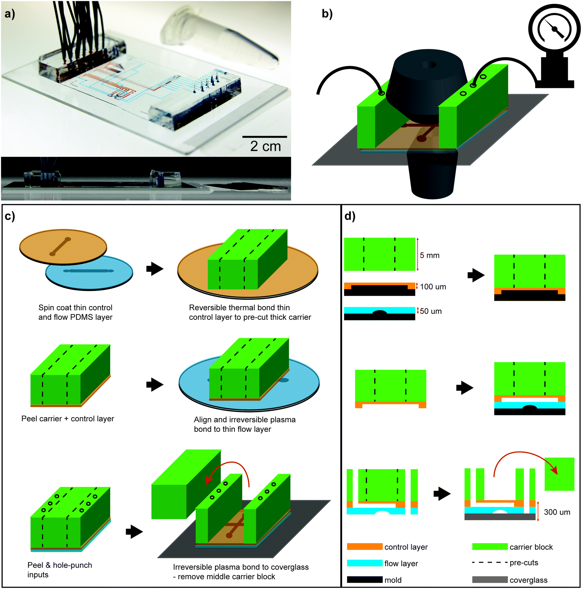 | ||
| Fig. 1 The thin valve-microfluidic chip. a) The angled (top) and side (bottom) view of the thin-chip with food coloring in the control channels with a 1.5 mL Eppendorf tube (top) and a razor blade (bottom) for size comparison. The input bus (thick region) is ∼1 centimeter and the viewing window (thin region) is <250 μm thick (2 cm scale bar in photo). b) A schematic of the thin-chip loaded between a high NA condenser and objective on an inverted microscope. c) A schematic of the thin-chip fabrication protocol in 3D and d) in 2D xz cross section. The layers and features are labeled in d). | ||
Our strategy to handle and align two thin layers was to utilize a thick ‘carrier’ layer with a pre-cut detachable block (Fig. 1c and d and S1†) during the fabrication process. The carrier layer was designed to bond and transfer the thin valve layer to the thin flow layer while providing rigidity and support during alignment. After alignment and final bonding to the glass substrate, a portion of the carrier layer was detached to expose the thin viewing window. The remaining carrier region would become the bus for the pin connector interface (Fig. 1a).
Designing this protocol required optimizing the relative bonding strength between the multiple layers, so that thin control and flow layers can be effectively transferred from the mold to the substrate and that the carrier layer can be selectively removed. Specifically, peeling the detachment block from the carrier layer requires that only the carrier layer is removed while the two thin layers below remains attached to the glass (Fig. 1c and d and S1†). To achieve this, we compared various bonding methods and parameters including thermal, plasma, and adhesive bonding and found the most robust solution.
Bond strengths between two different PDMS layers and glass can be tuned by adjusting the bonding method such as plasma or thermal bonding as well as controlling parameters like gas type, gas flow rate, plasma RF power,29 and baking temperature and duration. Optimized plasma and thermal bonding methods both generate bonds capable of withstanding valve control pressures of above 30 PSI. However, the uniformity and density of covalent bonds created through plasma bonding grants significantly stronger bonds than that of the thermal bonding. Taking advantage of this difference, we plasma bonded the thin layers to each other and to the glass substrate for permanent bonding while thermally bonding the carrier layer to the top thin layer to remove the detachable block. For fabrication reproducibility, we designed our protocol to use only the parameters that maximize bonding strengths for a given bonding method to give tolerance to PDMS batch effects and varying lab conditions.
Cover-glass substrates are required for high NA objectives; however, large thin cover-glasses are fragile and difficult to handle. PDMS chips bonded to cover-glass substrates can easily crack from the torque generated by the weight of the connected tubes. The fragile nature of cover-glass posed another serious challenge to fabricating the thin-chip during the detachment region peeling process as the peeling force cracked the glass. As a solution, we created an acrylic adapter and bonded it to our thin device with an adhesive for the needed sturdiness. Both the acrylic and adhesive film were laser cut and aligned to avoid masking of the viewing window (Fig. S2†). The adapter was also bigger than the cover-glass to support the entirety of the chip.
The thin-chip used in this study was designed to isolate, image, and sort single particles and cells (Fig. S3†). The device has three sample and buffer inputs, each, and is designed with eight sample outputs to interface with a column of a 96-well plate. To reduce the number of control channels, a flow multiplexer is integrated into the design.2 The imaging region is designed with an H-bridge fluid circuitry that reverses the flow direction to switch between the sample collection and waste modes. This design also minimizes the cell input and collection buffer channel overlap to prevent cross contamination. Using this chip, we achieved deterministic active sorting, actuated by complex high-resolution SRS imaging. After imaging, the cells were redirected to the sample outlets for collection or the waste channel.
Thin-chip performance characterization
We compared the valve actuation speed between thin- and thick chip with the same design. Valve actuation kinetics were determined by loading fluorescent dye in the device's flow channels and measuring the cumulative fluorescence in the flow channel directly beneath a valve transitions between open and closed states. The channel was the brightest at the open state and darkest at the closed state, since all the dye solution was pushed out of the flow channel when the valve is compressed. The fluorescence was measured by focusing the excitation beam on the center of the flow channel and the fluorescence emission was continuously collected with photomultiplier tube (PMT) with microsecond temporal resolution. We found that the thin-chip actuation rates were comparable to a traditional thick chip (Fig. 2a). | ||
| Fig. 2 Characterization of the thin-chip in comparison to the traditional thick chip. a) Valve opening and closing speed averaged over five operations. Black line denotes standard deviation of the mean error bar. b) A cartoon of the 2D xz cross section of the thick and thin-chip during valve operation (the color scheme is as follows: green, orange, and blue are the carrier, control, flow layers, respectively, and grey is the glass substrate). c) The chip pressure tolerance averaged over ten chips each with the black line indicating standard deviation of the mean. The bottom dotted line indicates the 25 PSI operation pressure and the top line indicates the pressure tolerance of the seal between the pin connector and input hole. Thin45 and Thin75 denotes thin-chips with 45 μm and 75 μm control layer thicknesses, respectively. d) The degree of PDMS membrane expansion comparison between the thin- and thick chip when pressurized for valving. The dotted line indicates the valve operation pressure at 25 psi. Each data point is an average with n = 5 and the error bars are standard deviation of the mean. | ||
Next, we compared the control pressure tolerance between the thin-chip and traditional thick chips. Common failure modes of microfluidic chips at high valve pressures are delamination of the PDMS–glass or PDMS–PDMS bonds, and connector pin–PDMS unsealing. Additionally, the valves on the thin-chips can ‘balloon’ and rupture upon pressurization due to high PDMS membrane flexibility at such low thickness (Fig. 2b). To compare control pressure tolerance, we fabricated multiple thick and thin-chips with 45 μm and 75 μm control layer thicknesses and increased the pressure at 5 PSI increments until the leakage occurred. Both the thick and thin-chips with 75 μm valve layer held above 50 PSI and only failed at the pin/PDMS connection with no delamination, while the thin-chips with 45 μm valves ruptured at 40 PSI (Fig. 2c). Thus, there was no substantial difference in pressure tolerance between the thick and 75 μm thin-chips. While the thermal bonds between the thick carrier block were “weaker” than the plasma bonds, they were optimized for maximum thermal bonding strength. As a result, the ‘bus’ block tolerated upwards of 50 PSI without delamination and did not break due to the torque from the weight of the connector tubes. The total PDMS thickness of the 75 μm thin-chips were 120 μm and under 300 μm including the cover-glass substrate. These chips fit easily between two high NA objectives and the operation pressure of 25 PSI is well below the valving pressure limits.
One major difference between the thin and the thick chips was the amount of membrane deformation when pressurized for valving. This difference is a result of the higher elasticity of the top PDMS layer in the thin-chip in contrast to the thick chip. We quantified the amount of PDMS expansion during valving as a function of varying valve pressures. We measured this by scanning the valve with a focused infrared beam spot in Z and increasing the valving pressure while collecting PDMS SRS (Fig. S4†). In our comparison, the membrane on top of the valves in the 75 μm thin-chip expands twice as much as the thick chip at the operation pressure (Fig. 2d), but this expansion did not affect the valve actuation performance or reproducibility.
Thin-chip facilitates SRS imaging
In addition to providing a label-free imaging technique that can characterize the native chemical composition of biological specimens, SRS has recently proven to be a powerful imaging modality to detect molecules with small biologically orthogonal molecular tags such as alkyl30 or deuterium bonds31 to measure the metabolic activity of a cell or highlight newly synthesized molecules. The Raman signal from these non-natural molecular bonds are comparatively weak, and thus difficult to deconvolute from the non-specific XPM signal. Thin-chips can improve SRS microscopy performance when imaging cells in a microfluidic device because of compatibility with the short-working distance objectives and condensers that are required to minimize XPM in SRS microscopy.To demonstrate this improvement in SRS imaging, HEK293T cells treated with D2O were imaged inside the trapping chamber of a thin-chip designed for single-cell sorting. We compared these images to the SRS images obtained in a traditional PDMS device with a long working distance condenser, by placing a 1 cm PDMS block on top of the thin-chip and re-imaging the cells (Fig. S5†). In this way we could directly compare images of the same cells between the thin- and thick chip configuration. We evaluated the performance of SRS imaging in the thin-chip by collecting images at two wavenumbers, 2950 cm−1, corresponding to CH3 stretches, with most of the contributing signal coming from proteins with a high fraction of CH3 bonds, and at 2135 cm−1 corresponding to C–D (D = deuterium) bonds that should only be present in the samples incubated with D2O (Fig. 3a). All images were acquired using a 1.2 NA water immersion objective. For images acquired in the thin-chip a 1.4 NA oil immersion condenser was used with a working distance of 1.6 mm. For the thick chip, a longer 5.4 mm working distance air condenser was used, with a NA of 0.8. The overall background level for the images acquired with the thick chip in the 2950 cm−1 channel was higher than that of the thin-chip, due to XPM signal contributions from the buffer (Fig. 3b). We also imaged cells sandwiched between two coverglasses with both the air and oil immersion condensers (Fig. S6†). While the coverglass images had slightly lower noise (Fig. 3b), this could be result of cell-to-cell variation as it was impossible to compare identical cells in both the thin-chip and coverglass. Additionally, the noise in the coverglass images using an air condenser was significantly higher than that from the thin-chip using an oil condenser, indicating XPM to be the highest source of background signal.
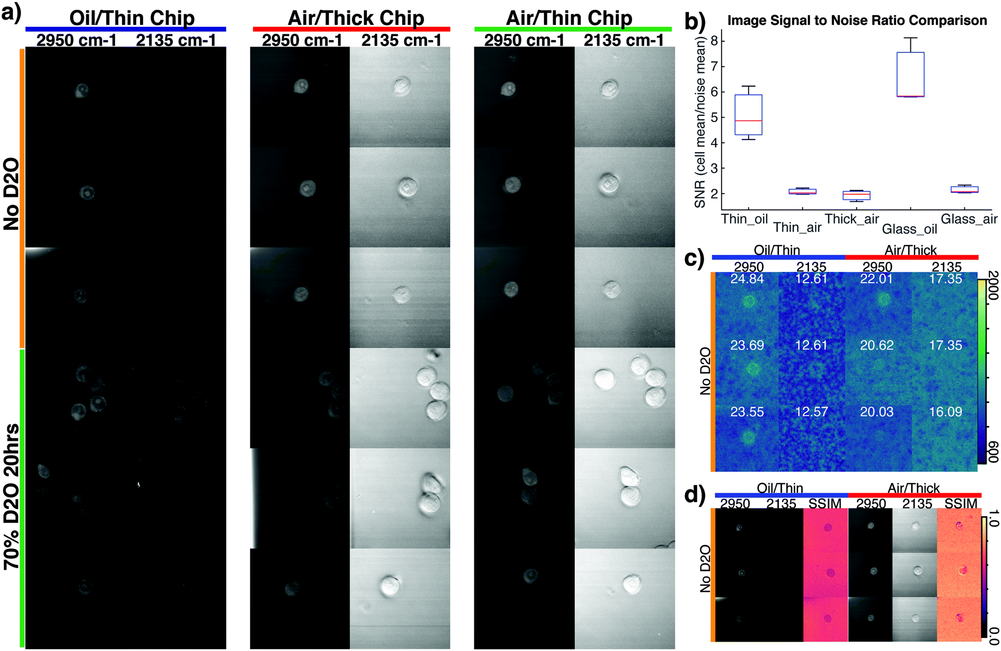 | ||
| Fig. 3 Single cell two-color SRS imaging using the thin and thick chip. a) SRS images of HEK293T cells with and without D2O incubation acquired at 2950 cm−1 and 2135 cm−1. Each group of two columns on the left, middle, and right corresponds to images acquired using the thin-chip and a 1.4 NA oil immersion condenser, the thick chip and a 0.8 NA air condenser, and the thin-chip using a 0.8 NA air condenser, respectively. b) The signal to noise ratio (SNR) of the images of the same cells in the thin- and thick chips with the oil immersion and air condenser are compared. The SNR of images of different cells on coverglass is also displayed. The SNR is calculated as the mean intensity of the cell areas over the mean intensity of the background. c) The local MSSoE maps for the 2135 cm−1 and 2950 cm−1 images, acquired with the thin-chip (left) and thick chip (right) of identical cells, and total MSSoE. The total MSSoE gives a measure of structural information across multiple scales. The maps indicate which areas of the image contributed most strongly to the measure, with yellow/green indicating greater contribution. d) The local structural similarity index metric (SSIM) images comparing the similarity between the two channels. The SSIM metric was calculated pixel by pixel with a rolling window of side length 11, using 3-pixel standard deviation gaussian weights. | ||
To further test the thin-chip's ability to remove XPM compared to traditional valve microfluidic devices for SRS cell imaging, we compared the true signal and artifacts caused by XPMin the 2135 cm−1 when imaging intracellular C–D bonds after cells metabolize heavy water. SRS images were acquired of D2O-incubated and non-incubated HEK293T cells in both the 2950 cm−1 and 2135 cm−1 channels. In this configuration, the Raman shift from the newly created deuterium tags can only be seen in the 2135 cm−1 channel, where no vibrational frequencies are present from native mammalian biomolecules. As is apparent in Fig. 3a, the images from the thin-chip clearly show SRS signal from the C–D bonds, which is exclusively seen in cells incubated in D2O. However, in the thick chip, the artifacts generated by signal from XPM exists in the 2135 cm−1 channel for both the D2O and non-D2O cells, making it difficult to detect the specific Raman contribution from the C–D bonds.
The SRS image improvements from using the thin-chip over thick chips can be quantitatively characterized by comparing the information of the images in both channels using a measure of the entropy of the image. Higher entropy, corresponding to better ability to discern structure, can be seen in cells in the 2950 cm−1 channel in the thin-chip. (Fig. 3c and S7†). Additionally, there should be no signal in the 2135 cm−1 channel when cells are not incubated with D2O and therefore the entropy should be lower. By removing XPM in this channel, the thin-chip demonstrates the expected reduction in entropy compared to the thick chip (Fig. 3c).
We also characterized the structural similarity between the images acquired at the two wavenumbers, using the structural similarity index measure (SSIM). For images acquired in the absence of the unwanted XPM signal, the structural similarity should be very low between these channels, as the 2135 cm−1 channel should contain only noise. However, there is relatively high structural similarity at the edges of the cells in the thick chip using the air condenser, indicating similar feature content (Fig. 3d and S8†). Note that while it seems that there is cell contrast in the SSIM images for the thin-chip and oil condenser, the metric actually indicates lower shared structure due to the transition from just noisy background to internal cell signal.
Magnetic bead manipulation in in the thin-chip
To verify the potential of sorting cells with antibody coated magnetic beads using our thin-chip, we validated our ability to immobilize a small number of magnetic beads in a flow field. For this test, we imaged fluorescently labeled 3 μm diameter magnetic beads in the flow channel at varying flow pressure while positioning a rare earth magnet above the trapping chamber (Fig. 4a). In our experiment, we successfully immobilized few isolated magnetic beads and resisted up to 3 PSI flow pressure by placing the magnet directly on top of the chip. In contrast, the beads were unable to resist our lowest flow pressure of 0.5 PSI when the magnet was lifted more than 1 mm (Fig. 4b and S9 and Video S1†). We also examined the contribution of channel deformation due to flow pressure in this experiment and found it to be negligent (Fig. S10†). This result shows the clear advantage of using the thin-chip to control and immobilize magnetic beads in the presence of flow that posed a challenge in traditional valve-microfluidic due to its centimeter thickness and the low magnetic susceptibility of microbeads. | ||
| Fig. 4 Magnetic bead control demonstration on valve-microfluidic chips. a) A cartoon of the experimental setup where the thin-chip was loaded on an inverted microscope. The compact magnet with manual height position control was placed on top of the chip. Magnetic beads were injected into the chip by a tube and a regulated external pressure source. b) A plot of 3 μm magnetic bead velocity at varying flow pressures in the thin-chip with a stationary magnet placed directly on top. The bead velocity was measured after the flow reached a steady state. The blue dotted line indicates the threshold where the sheer force (FS) dominated the magnetic force (FM) that held the beads in place and resisted flow (blue, 0 mm). The shear force overwhelmed the magnetic force when the magnet was raised to more than 1 mm above the surface of the thin-chip at even our lowest pressure setting of 0.5 psi (red). Each data point is an average of n = 5 separate beads and the error bar is the standard deviation. c) Reversible 1 μm SPRI bead column creation in the flow channel of the chips with an external magnet. The three images in each column are sequential snapshots of the flow channel with changes in valve states and magnet placement. The external magnet was placed slightly off-center to enable top illumination. | ||
Next, we aimed to demonstrate our ability to create reversible magnetic bead columns in our thin-chip using a common magnet. For this validation, we imaged the flow channel of the thin-chip while flowing 1 μm SPRI beads at 5 to 10 PSI with and without the external magnet placed on top of the chip. To compare this with the thick chip, we performed the same experiment with a 1 cm thick PDMS block placed between the magnet and the surface of the thin-chip (Fig. S5†). Our results demonstrate that the magnetic bead columns can only be generated in the flow channels of the thin-chip while simultaneously imaging with an inverted fluorescent microscope (Fig. 4c).
Discussion
We developed a new generation of paper-thin integrated valve-microfluidic devices with a thickness of less than 300 μm. We demonstrated that the thin-chip valves display comparable functionality, reliability and operation speed to traditional multilayer integrated devices with orders of magnitude reduction in thickness. We demonstrated the advantages of our thin-chip with two-color SRS imaging of live single cells, where our thin-chip generated superior image quality with increased resolution and signal-to-noise ratio compared to traditional thick chips. Combining SRS imaging with integrated valve-microfluidics enables many new applications, including single-cell sorting based on high-resolution hyper-spectral SRS imaging. Joined with RNA sequencing, this can add information about chemical composition and morphological information to single cell profiles32 for discovering new cell types and related marker genes.Using our thin-chip, we also demonstrated the ability to simultaneously perform high-magnification imaging while manipulating magnetic beads on an integrated valve-microfluidic chip. The ability to automate and program solution exchange steps will greatly benefit the field of magnetic tweezers. Although magnetic tweezing is a powerful platform to study conformational dynamics and forces that act on single-molecule, these experiments are inherently low-throughput which limits the number of conditions and replicates that can be performed in an experiment. Because biomolecules interact with many different molecules in an extremely large chemical space in physiological conditions, it is impossible to manually quantify each interaction at a meaningful scale.33 With the thin-chip, the magnetic tweezing community can take advantage of the automated large-scale experimental capability of valve-microfluidics.
The ability to immobilize magnetic beads in the thin-chip while being compatible with inverted microscopes also opens new possibilities for high dimensional multi-omics measurement of single cells. For example, reversible bead columns can be produced for protein or DNA purification by packing magnetic beads in the flow channel with an external magnet. Antibody-coated beads can also be immobilized in the thin-chip at low density and be used to bind and enrich cells based on their surface proteins, as “programmable” microfluidic pillar arrays.34,35 Immobilized bead-based cell capturing is advantageous over fabricated microfluidic pillars in that it can be readily implemented and integrated into existing chips, and dynamically modified to detect vastly more cell markers by simply changing the beads during a single chip run. In combination with both imaging and downstream genomic analysis, such a method can enable multidimensional cell profiling.
Finally, the flexibility of the thin-chip technology also enables the possibility of implementing microfluidic valves and active fluidic control in the rapidly growing field of flexible-thin microfluidics for wearable devices. For example, recent PDMS-based sweat sensors could implement integrated valves for multiplexed assays using the thin-chip technology described here.36,37 Paper-thin valve-microfluidic devices combine the advantages of integrated microfluidic circuits with the thin form-factor of integrated electronic circuits representing a major step in the application of microfluidic large-scale integration.
Methods
Microfabrication
The thin chip was fabricated at UC Berkeley by soft lithography, where PDMS was casted on a photoresist patterned silicon wafer mold. Three separate molds were used to make the 1 cm carrier, 45 μm control, and the 75 μm flow layer. The carrier was pre-cut and partially cured before thermal bonding to the control layer. The control layer on the carrier was then manually aligned and oxygen plasma bonded to the flow layer. After hole punching the input and output ports, the three-layer PDMS chip was then plasma bonded to a number 1.5 cover-glass. Finally, the resulting product was bonded to a laser cut acrylic adapter and the removable middle portion of the carrier was peeled to reveal the 110 μm thick imaging region.The molds were fabricated using standard micron photolithography. The flow layer mold was patterned in three steps: (1) rounded 30 μm, (2) rectangular 5 μm, and (3) rectangular 30 μm features. The rounded features were produced by spin-coating AZ40XT photoresist (IMM) on a hexamethyldisilazane (Sigma) coated 4 inch silicon wafer (University Wafers), patterning with 365 nm ultraviolet exposure (OAI 206) through a mask designed (AutoCAD) and printed at 20![[thin space (1/6-em)]](https://www.rsc.org/images/entities/char_2009.gif) 000 dpi (CAD/ART), developing in the 300 MIF developer (IMM), then slowly heating from 65 °C to 190 °C with a 10 °C per hour ramp. The rectangular features were serially added to the mold by spin-coating, aligning, and UV exposing SU-82005 photoresist (Kayaku) to 5 μm and SU-83025 (Kayaku) to 30 μm then developing in SU-8 developer (Kayaku). The control and carrier layers were single layer molds that were fabricated by spin-coating 30 μm of SU-83025 photoresist on a silicon wafer, followed by UV exposing and developing. The molds were treated with trichloromethylsilane (Sigma) before soft lithography.
000 dpi (CAD/ART), developing in the 300 MIF developer (IMM), then slowly heating from 65 °C to 190 °C with a 10 °C per hour ramp. The rectangular features were serially added to the mold by spin-coating, aligning, and UV exposing SU-82005 photoresist (Kayaku) to 5 μm and SU-83025 (Kayaku) to 30 μm then developing in SU-8 developer (Kayaku). The control and carrier layers were single layer molds that were fabricated by spin-coating 30 μm of SU-83025 photoresist on a silicon wafer, followed by UV exposing and developing. The molds were treated with trichloromethylsilane (Sigma) before soft lithography.
The PDMS chip fabrication was done with standard on-ratio bonding multilayer soft lithography protocols. PDMS (Momentive) was mixed at 10:1 silicone to crosslinker ratio and degassed on an orbital mixer (Thinky AR250), poured onto the carrier mold, and partially cured by baking at 70 °C for 24 minutes. To enable the removal of the middle block, the carrier was scored on the bottom along the two middle block indicators, leaving 1 mm from the top. This was done by placing 1 mm thick substrates (glass slides) on each of the opposing edges of the top-side-down carrier and then cutting through with a razor blade until it is stopped by the substrates, which leaves an uncut 1 mm gap from the top of the carrier layer (Fig. S1a†). The same PDMS mix was spin-coated on the control and flow layer mold to 45 μm and 75 μm, respectively, and baked at 70 °C for 14 minutes. The pre-cut carrier was manually aligned to the control layer and thermally bonded by baking at 70 °C for 5 minutes. The carrier-control layer intermediate composite was plasma bonded to the flow layer by exposing control and flow layers to oxygen plasma (plasma equipment technical RIE) for 10 seconds at 0.283 mTorr with 20 W power, then manually aligning under a stereomicroscope (Nikon). After peeling the carrier-control-flow composite from the flow layer mold, the chip was hole punched (Syneo, ID 660 μm tips) on the designated inlet/outlet ports. The chip was then plasma (brand) bonded to a number 1.5 cover-glass (Thomas Scientific) by exposing to oxygen plasma for 22 seconds at 0.283 mTorr with 20 W power. The entire assembly was then bonded to a laser cut ⅛ inch acrylic adapter (Fig. S2†) with double-sided tape (3M 468MP). The center portion of the carrier was removed by cutting (Fig. S1b†) the 1 mm remaining portion on top with a razor blade then carefully peeling off. The final product was baked at 70 °C for 2 hours.
Microfluidic controller and chip operation
The flow and control pressures were activated by KATARA (http://streetslab.berkeley.edu/tools/katara/) that controlled an array of solenoid valves (Pneumadyne) connected to the computer by a USB interface (Arduino Mega).The valve operation pressure was 25 psi and the flow pressure were varied between 0.5 to 10 PSI using a high-resolution manual pressure regulator. The surface of the flow channels in the microfluidic chip was passivated with 0.5% w/v Pluronic F-127 (Sigma) in water for 10 minutes to reduce bead and cell adsorption.
SRS microscopy
The synchronized dual output of a femtosecond oscillator/OPO (Insight DS+, Spectra-Physics) provided the pump (tunable OPO output), and Stokes beams (fundamental at 1040 nm) for the experiment. The power of both beams was controlled using two variable attenuators consisting of a half-wave Fresnel rhomb (for the pump), or half-wave plate (for the Stokes), and a polarizer. The pump beam was tuned to 796 nm for CH2/CH3 imaging, and 851 nm for off-resonance imaging, corresponding to Raman shifts of 2950 cm−1 and 2135 cm−1. The actual spectral bandwidth was ∼160 cm−1 due to the short pulse duration of ∼120 fs. The output from the Stokes beam was then intensity modulated at 10.28 MHz using a quarter waveplate (Thorlabs), a resonant electro-optic modulator (EOM; Thorlabs) and a Glan-laser polarizer (Thorlabs). The resonant EOM was driven by a function generator (33120A, Hewlett Packard), and an additional power amplifier (ZHL-32A+, Minicircuits). The pump beam path length was controlled by an optical delay line (FCL200, Newport) to ensure coincident arrival of the pulses of the two beams. The beams were then combined on a 1000 nm short-pass dichroic mirror (Thorlabs), and fed into the scan head of a confocal scanning microscope (FV1200, Olympus). The beams were delivered to the sample by a near infrared optimized 60× water immersion objective with a numerical aperture (NA) of 1.2 (UPLSAPO60XWIR, Olympus). After the sample, the lasers were collected by a 1.4 NA oil condenser (CSC1003, Thorlabs; or equivalently D-CUO, Nikon) or 0.8 NA air condenser. The Stokes beam was then filtered by a 1000 nm shortpass filter (Thorlabs). A series of relay lenses delivered the pump beam to a photodiode (S3590-08, Hamamatsu), reverse biased at 61.425 V (Keysight). The signal from the photodiode was bandpass filtered and fed into a lock-in amplifier (HF2LI, Zurich Instruments) for image formation. The power of the Stokes beam was set to 30 mW at the sample, and the power of pump was set to 30 mW, and the images were acquired at a size of 512 × 512 using a pixel dwell time of 2 μs and a lock-in time constant of 1 μs.Two photon imaging
For two photon fluorescence imaging the output of the OPO was tuned to 900 nm, and delivered to the sample using the pump excitation path described above. The power was set to 20 mW, and a pixel dwell time of 2 μs was used to collect time series from a single point in the center of the image.Magnetic bead control in the thin-chip
For the single bead immobilization experiment, 3 μm Flash Red fluorescent dye coated beads (Bangs Labs) were diluted to 0.1% w/v in 1× PBS buffer with 0.5% Tween20, and injected into the thin-chip mounted on the inverted microscope. While imaging the fluorescent beads with 60× water immersion objective and two-photon excitation, the flow pressure was varied from 0.5 to 4.5 PSI. The magnetic field strength was also controlled by moving a stack of ten 10 mm diameter and 2 mm thick neodymium disc magnets mounted on the center of the condenser holder (and field of view).For the reversible magnetic bead column creation experiment, 1 × 1 μm SPRI beads (Beckman) in 1× PBS buffer with 0.5% Tween20 were injected into the thin-chip. While imaging the beads in the flow channel with bright-field microscopy under 5 to 10 PSI flow pressure, the magnet stack was placed as close to the flow channel without blocking the illumination. Four different conditions were imaged, magnet on/off and valve on/off, to test if the magnetic bead column can be formed. To mimic the traditionally fabricated thick chip, we placed a clean 1 cm PDMS block on top of the mounted thin-chip and repeated the experiment.
Cell culturing
Human embryonic kidney (HEK293T) cells (UC Berkeley cell culture facility) were cultured in Dulbecco's Modified Eagle Medium (DMEM) with L-glutamine and without pyruvate, including 10% fetal bovine serum (FBS), and 1% penicillin/streptomycin. Cells were passaged upon achieving between 70–100% confluency. Cells were imaged at 50–70% confluency. Cells were transferred to and imaged in the live cell imaging solution (Fisher Sci).To deuterium tag cells, the D2O (Sigma) DMEM media was made by mixing 70% D2O (Sigma) with 30% deionized H2O to dissolve DMEM powder (Sigma), 10% fetal bovine serum (FBS), 1% penicillin/streptomycin, and 3.7 g L−1 sodium bicarbonate (Sigma). After pH adjusting to 7.4, the media was sterilized with a 0.2 μm filter. The cell media was replaced with the D2O media at 50–70% cell confluency then incubated for 20–24 hours. The cells were transferred to and imaged in the live cell imaging solution with 70% D2O.
Structural similarity calculation (SSIM)
The SSIM was computed between the 2135 cm−1 and 2950 cm−1 images using a rolling window of side length 11 with Gaussian weights corresponding to σ = 3. The metric defined between the patches, x and y, for the 2135 cm−1 and 2950 cm−1 channels respectively, is given by:where μ are the means, σ2 the variances, and σxy the covariance. The scale was renormalized to 0 to 1. The individual values reported are the means over the SSIM images.

Entropy (MSSoE)
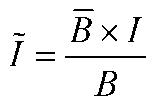
All images, I, were pseudo-flatfield corrected prior to calculation. An estimate of the background power distribution, B, was obtained by first median filtering the image with a radius of 200. The corrected images, Ĩ, were obtained according to the following equation:with the bar denoting the mean of the background. The images were then rescaled from their minima to maxima, for maximum contrast, and processed at a bit depth of 16.
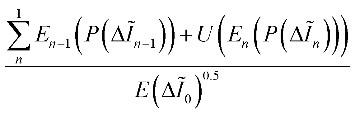
For a measure of structural information as opposed to uncertainty the multi-scale second order entropy (MSSoE) was calculated using the second-order probability Q(P(·)).38 To incorporate information from multiple spatial scales, and emphasize edges, the second-order entropy was computed for each level of a Laplacian pyramid {ΔĨn}, and summed across levels, as proposed by Rakshit and Mishra.39 The pyramid was constructed with a scaling factor of two, to a final layer that was 16 × 16 pixels. The final MSSoE is given by:

For visualization of the features that most strongly contributed to the metric, entropy maps, {En(P(ΔĨn))}, were created for each level of the pyramid. The final map was then reconstructed layer by layer, upscaling by a factor of 2 through bilinear interpolation, and summing the result. Through summation, features that show a comparatively high entropy in the final image either contributed across multiple spatial scales, or strongly on at least one. The final images were normalized to the first-order entropy calculated on the first layer of the pyramid E(ΔĨ0), which provides a degree of noise suppression. With U as the upscaling operator, the procedure is given by, with summation over decreasing n:
the level of statistical significance was determined through comparison to tabulated critical U values.40

Conflicts of interest
There are no conflicts to declare.Acknowledgements
We thank Annie Maslan and Anushka Gupta for providing us with the cells for SRS imaging, Dr. Nicolas Altemose for taking photos of the thin-chip, and other members of the Streets Lab for helpful discussions. This work was supported in part by National Natural Science Foundation of China (81950410636), and the Li Dak Sum Yip Yio Chin Kenneth Li Marine Biopharmaceutical Development Fund. Aaron Streets is a Chan Zuckerberg Biohub investigator.References
- T. Thorsen, S. J. Maerkl and S. R. Quake, Science, 2002, 298, 580–584 CrossRef CAS PubMed.
- S. Kim, A. M. Streets, R. R. Lin, S. R. Quake, S. Weiss and D. S. Majumdar, Nat. Methods, 2011, 8, 242–245 CrossRef CAS PubMed.
- S. Kim, J. De Jonghe, A. B. Kulesa, D. Feldman, T. Vatanen, R. P. Bhattacharyya, B. Berdy, J. Gomez, J. Nolan, S. Epstein and P. C. Blainey, Nat. Commun., 2017, 8, 13919 CrossRef CAS PubMed.
- B. Y. Yu, C. Elbuken, C. Shen, J. P. Huissoon and C. L. Ren, Sci. Rep., 2018, 8, 1–12 Search PubMed.
- A. M. Streets, X. Zhang, C. Cao, Y. Pang, X. Wu, L. Xiong, L. Yang, Y. Fu, L. Zhao, F. Tang and Y. Huang, Proc. Natl. Acad. Sci. U. S. A., 2014, 111, 7048–7053 CrossRef CAS PubMed.
- Y. Marcy, C. Ouverney, E. M. Bik, T. Lösekann, N. Ivanova, H. G. Martin, E. Szeto, D. Platt, P. Hugenholtz, D. A. Relman and S. R. Quake, Proc. Natl. Acad. Sci. U. S. A., 2007, 104, 11889–11894 CrossRef CAS PubMed.
- Z. C. Landry, S. J. Giovanonni, S. R. Quake and P. C. Blainey, in Methods in Enzymology, Academic Press Inc., 2013, vol. 531, pp. 61–90 Search PubMed.
- M. Noach-Hirsh, H. Nevenzal, Y. Glick, E. Chorni, D. Avrahami, E. Barbiro-Michaely, D. Gerber and A. Tzur, Mol. Cell. Proteomics, 2015, 14, 2824–2832 CrossRef CAS PubMed.
- C. Furlan, R. A. M. Dirks, P. C. Thomas, R. C. Jones, J. Wang, M. Lynch, H. Marks and M. Vermeulen, Nat. Commun., 2019, 10, 1–8 CrossRef CAS.
- R. Gómez-Sjöberg, A. A. Leyrat, D. M. Pirone, C. S. Chen and S. R. Quake, Anal. Chem., 2007, 79, 8557–8563 CrossRef PubMed.
- F. K. Balagaddé, L. You, C. L. Hansen, F. H. Arnold and S. R. Quake, Science, 2005, 309, 137–140 CrossRef PubMed.
- A. R. Wheeler, W. R. Throndset, R. J. Whelan, A. M. Leach, R. N. Zare, Y. H. Liao, K. Farrell, I. D. Manger and A. Daridon, Anal. Chem., 2003, 75, 3581–3586 CrossRef CAS PubMed.
- C. W. Freudiger, W. Min, B. G. Saar, S. Lu, G. R. Holtom, C. He, J. C. Tsai, J. X. Kang and X. S. Xie, Science, 2008, 322, 1857–1861 CrossRef CAS PubMed.
- W. J. Greenleaf, K. L. Frieda, D. A. N. Foster, M. T. Woodside and S. M. Block, Science, 2008, 319, 630–633 CrossRef CAS PubMed.
- E. Ostrofet, F. S. Papini and D. Dulin, Sci. Rep., 2018, 8, 2–11 CrossRef PubMed.
- A. Chronopoulos, S. D. Thorpe, E. Cortes, D. Lachowski, A. J. Rice, V. V. Mykuliak, T. Róg, D. A. Lee, V. P. Hytönen and A. E. del Río Hernández, Nat. Mater., 2020, 19, 669–678 CrossRef CAS PubMed.
- M. Srisa-Art, S. D. Noblitt, A. T. Krummel and C. S. Henry, Anal. Chim. Acta, 2018, 1021, 95–102 CrossRef CAS PubMed.
- M. Suzuki, T. Sakashita, Y. Hattori, Y. Yokota, Y. Kobayashi and T. Funayama, J. Neurosci. Methods, 2018, 306, 32–37 CrossRef CAS PubMed.
- M. Zhang, J. Wu, L. Wang, K. Xiao and W. Wen, Lab Chip, 2010, 10, 1199–1203 RSC.
- J. Huft, D. J. Da Costa, D. Walker and C. L. Hansen, Lab Chip, 2010, 10, 2358–2365 RSC.
- M. P. Cuchiara, A. C. B. Allen, T. M. Chen, J. S. Miller and J. L. West, Biomaterials, 2010, 31, 5491–5497 CrossRef CAS PubMed.
- M. Tonin, N. Descharmes and R. Houdré, Lab Chip, 2016, 16, 465–470 RSC.
- W. H. Grover, M. G. Von Muhlen and S. R. Manalis, Lab Chip, 2008, 8, 913–918 RSC.
- Y. Yalikun and Y. Tanaka, Micromachines, 2016, 7, 83 CrossRef PubMed.
- T. Wang, J. Chen, T. Zhou and L. Song, Micromachines, 2018, 9, 269 CrossRef PubMed.
- B. G. Saar, C. W. Freudiger, J. Reichman, C. M. Stanley, G. R. Holtom and X. S. Xie, Science, 2010, 330, 1368–1370 CrossRef CAS PubMed.
- J. X. Cheng and X. S. Xie, Coherent Raman Scatt. Microsc., 2016, pp. 1–610 Search PubMed.
- K. I. Popov, A. F. Pegoraro, A. Stolow and L. Ramunno, Opt. Lett., 2012, 37, 473 CrossRef CAS PubMed.
- S. Bhattacharya, A. Datta, J. M. Berg and S. Gangopadhyay, J. Microelectromech. Syst., 2005, 14, 590–597 CAS.
- H. Yamakoshi, K. Dodo, M. Okada, J. Ando, A. Palonpon, K. Fujita, S. Kawata and M. Sodeoka, J. Am. Chem. Soc., 2011, 133, 6102–6105 CrossRef CAS PubMed.
- L. Shi, C. Zheng, Y. Shen, Z. Chen, E. S. Silveira, L. Zhang, M. Wei, C. Liu, C. de Sena-Tomas, K. Targoff and W. Min, Nat. Commun., 2018, 9, 1–17 CrossRef PubMed.
- T. N. Chen, A. Gupta, M. D. Zalavadia and A. Streets, Lab Chip, 2020, 20, 3899–3913 RSC.
- S. Le, M. Yao, J. Chen, A. K. Efremov, S. Azimi and J. Yan, Nucleic Acids Res., 2015, 43, 113 CrossRef PubMed.
- S. Wang, K. Liu, J. Liu, Z. T. F. Yu, X. Xu, L. Zhao, T. Lee, E. K. Lee, J. Reiss, Y. K. Lee, L. W. K. Chung, J. Huang, M. Rettig, D. Seligson, K. N. Duraiswamy, C. K. F. Shen and H. R. Tseng, Angew. Chem., Int. Ed., 2011, 50, 3084–3088 CrossRef CAS PubMed.
- S. Hou, J. F. Chen, M. Song, Y. Zhu, Y. J. Jan, S. H. Chen, T. H. Weng, D. A. Ling, S. F. Chen, T. Ro, A. J. Liang, T. Lee, H. Jin, M. Li, L. Liu, Y. S. Hsiao, P. Chen, H. H. Yu, M. S. Tsai, M. D. Pisarska, A. Chen, L. C. Chen and H. R. Tseng, ACS Nano, 2017, 11, 8167–8177 CrossRef CAS PubMed.
- J. C. Yeo, J. Yu, Z. M. Koh, Z. Wang and C. T. Lim, Lab Chip, 2016, 16, 3244–3250 RSC.
- A. Koh, D. Kang, Y. Xue, S. Lee, R. M. Pielak, J. Kim, T. Hwang, S. Min, A. Banks, P. Bastien, M. C. Manco, L. Wang, K. R. Ammann, K. I. Jang, P. Won, S. Han, R. Ghaffari, U. Paik, M. J. Slepian, G. Balooch, Y. Huang and J. A. Rogers, Sci. Transl. Med., 2016, 8, 366ra165 CrossRef PubMed.
- J. Baron, Second-order probabilities and belief functions, Theory Decis., 1987, 23, 25–36 CrossRef.
- S. Rakshit and A. Mishra, ed. P. J. Narayanan, S. K. Nayar and H.-Y. Shum, Springer Berlin Heidelberg, Berlin, Heidelberg, 2006, pp. 265–275.
- F. Sani and J. Todman, Frontmatter, 2006 Search PubMed.
Footnotes |
| † Electronic supplementary information (ESI) available. See DOI: 10.1039/d0lc01217c |
| ‡ Correspondence and requests for materials should be addressed to Aaron Streets (astreets@berkeley.edu). |
| This journal is © The Royal Society of Chemistry 2021 |