
High-resolution integrated piezoresistive sensors for microfluidic monitoring†
Yongxiao
Zhou
a,
Erik M.
Werner
 a,
Eugene
Lee
b,
Michael
Chu
a,
Thao
Nguyen
c,
Kevin D.
Costa
bd,
Elliot E.
Hui
a and
Michelle
Khine
*ab
a,
Eugene
Lee
b,
Michael
Chu
a,
Thao
Nguyen
c,
Kevin D.
Costa
bd,
Elliot E.
Hui
a and
Michelle
Khine
*ab
aDepartment of Biomedical Engineering, University of California, Irvine, CA 92697, USA. E-mail: mkhine@uci.edu
bNovoheart, Vancouver, Canada
cDepartment of Chemical and Biomolecular Engineering, University of California, Irvine, CA, USA
dCardiovascular Research Center, Icahn School of Medicine at Mount Sinai, New York, NY, USA
First published on 10th December 2020
Abstract
Microfluidic devices are traditionally monitored by bulky and expensive off-chip sensors. We have developed a soft piezoresistive sensor capable of measuring micron-level strains that can be easily integrated into devices via soft lithography. We apply this sensor to achieve fast and localized monitoring of pressure, flow, and valve actuation.
Introduction
Microfluidic devices for various applications – including molecular analysis, cellular analysis, and drug screening – require precise control of parameters such as pressure and flow rate.1–6 Fluid delivery is typically accomplished using off-chip hardware including pressure regulators for pressure driven flow and syringe pumps to control volumetric flow. While routing and switching of fluids can be accomplished on-chip using integrated valves,7–9 they are ultimately controlled by external pressure sources and solenoids. Feedback from these systems, including parameters such as pressure or flow rate, are typically provided by sensors off-chip, located either in the tubing connected to the device or integrated into the perfusion hardware.Despite tremendous advances of micro total analysis systems in recent years, widely accessible on-chip monitoring and closed loop control of fundamental parameters are still lacking. The dearth of on-chip monitoring solutions creates inherent limitations in the responsiveness and accuracy of the measurements that can be obtained. Off-chip hydraulic and pneumatic sensors are limited by the dead volume of the interface tubing connecting the sensors to the chip. This dead volume is typically large compared to the volume of the microfluidic device itself and can be the dominant factor in determining the response time and accuracy of a measurement.
Currently available options for local measurement of these parameters are difficult to integrate into microfluidic systems. While optical sensors can produce accurate, reliable, and robust flow and pressure measurements, they still require coupling to expensive and complicated imaging systems.10–13 Micro electromechanical systems (MEMS)-based sensors offer on-chip integration with high resolution but typically involve complex fabrication and contact-based measurements. For example, in-channel sensors that extend into the fluid channel affect the local flow profile and can suffer from confounding factors including fouling; increased drag force from fouling can cause inaccurate results.14 Also, unlike microfluidic devices, commercially available MEMS sensors are not intended for single-use applications; hence this mismatch in cost and complexity has prevented more pervasive integration.15
Soft, stretchable sensors have attracted research interest due to their ability to conform to different surfaces and their large dynamic range under deformation. These sensors convert mechanical displacement into electrical signals such as resistance or capacitance change. Liquid metal-based pressure sensors with a polydimethylsiloxane (PDMS) substrate can be easily integrated into microfluidic devices. However, channels that contain liquid metal require extra precautions during fabrication or are more prone to mechanical failure. Alternatively, thin metal film-based sensors are easier and safer to fabricate and handle while offering attractive performance and robustness characteristics.16–18 Due to their physical properties, these metal thin film based sensors are able to sense mechanical deformations in various planes; the resulting electrical signals can be correlated and calibrated to physical parameters-of-interest. However, these soft strain gauges, have been typically limited to macroscale applications.19–21 There are few reports of soft sensors capable of monitoring micro-scale strains. Even recent papers focused on micron-scale sensors still report monitoring deformations on the millimeter scale.22 The ability to monitor deformations from extremely small forces requires unique strategies. For instance, wearable sensors may not respond as linearly in this micro regime as in macro-level, and gauge factor has been reported to be different between low strain range and high strain range.23,24 Secondly, in micro-applications, the system may not be able to actuate the strain sensor due to limited force output (e.g. the small force generated from a monolayer of cardiomyocytes, or small pressure changes in a microfluidic channel). The stress generated by an isolated muscle strip ranges from 8 to 20.7 kPa,25 which is not strong enough to drive conventional rigid force gauges.
To date, there are a limited number of papers that have demonstrated the effective application of flexible sensors in micro-device monitoring.24,26 Parker and colleagues developed a high-sensitivity piezoresistive sensor using multi-material 3D printing to monitor stress induced by cardiac tissues, with a reported minimum tested strain of 0.0125%.26 Flexible sensors such as this have the potential to replace traditional optical methods to monitor tissue contractility.27 Wen and colleagues developed a silver powder doped-PDMS based piezoresistive pressure sensor that can be bonded to a microfluidic device.24 When the pressure in the channel increases, the flexible sensor is stretched.
In situations of pressure driven flow, the pressure is directly proportional to flow rate. Thus, the flow rate can be calculated from the pressure measured by a sensor in the fluid channel. While most reported noncontact flow meters have a resolution of tens to hundreds of μl min−1,28–30 some research groups have demonstrated nanoliter resolution temperature flow sensors31 and 0.5 μl min−1 resolution microwave flow sensors.32 However, temperature flow sensors31 could be disturbed by non-flow effects, such as environmental heat flux flowing into sensors during experiments. Unlike other parameters, pressure is still a flow indicator that is independent from surrounding noise such as electromagnetic waves and heat flux. In the flow sensor by Sanati-Nezhad and colleagues, pressure in a microfluidic channel deforms a membrane to modulate the permittivity of a microwave resonator, thus producing a flow measurement.32
From the current literature on available sensors for micron scale in situ monitoring, there remains the need to develop a universal sensor compatible with soft lithography that can be scaled, arrayed, and used to measure a range of critical microfluidic parameters.
In this paper, we present a completely encapsulated wrinkled metal thin film based flexible piezoresistive sensor with tunable elastic modulus that can measure micron-scale strain, microfluidic device pressure, and valve state. This soft strain sensor has a dynamic range of 50% and can detect linear displacements as small as 5 μm (0.025% strain). The displacement of the sensor can be used to calculate the force applied to the sensor. Due to its high strain sensitivity to linear stretching and ultra-soft substrate, small pressures applied on the surface will deform the sensor, causing it to expand orthogonally to serve as a highly sensitive pressure sensor for microfluidic applications. The pressure measured from the microfluidic device can be correlated to flow rate in the channel as well. Finally, the sensor can be integrated into a pneumatic valve to monitor valve actuation. To the best of our knowledge, there is no such sensor that can electrically monitor valve state in microfluidic devices.
Results and discussion
Characterization of sensor performance
We first characterized our piezoresistive sensors with integrated nano-to-micro scale wrinkled structures (Fig. 1). This thin film is supported on and encapsulated within a silicone elastomer. The resistance change of the sensors is based on crack formation within the wrinkled film when stretched. When the sensor is strained linearly, deformation of the substrate causes elongation of the metal thin film. In comparison to planar thin films, the wrinkled film allows for a considerably larger dynamic range because the wrinkles unfold, align to the axis of strain, and stretch before cracks form. The subsequent cracking corresponds to a steeper increase in resistance as the cracks propagate and coalesce. In Fig. 1a, wrinkles were observed to stretch along the direction of the applied strain, indicated by the arrow. Cracks were formed as well. The red pseudo-color illustrates the exposed bottom polymer substrate and the cracks around it. The wrinkles act as additional strain relief, allowing for considerably larger dynamic range, while maintaining high sensitivity, before irreversible failure. | ||
| Fig. 1 (a) Unstretched (top) and stretched (bottom) sensors. On the right are scanning electron microscope images of sensor trace region. It is apparent on the SEM that the wrinkles align and stress in the direction of actuation. Fractures in the thin film have been illustrated by pseudo-coloring the exposed polymer layer in red. (b) Sensor's resistance response under different cyclic frequencies (from top to bottom are 0.5, 1, and 2 Hz respectively). The sensor (blue) tracks the displacement of 5 μm (red) very well, and the baseline shift is captured for 2 Hz as well (∼265 s). 5 μm corresponds to 0.025% strain of the sensor. (c) Representative sensitivity curve plotting change in resistance as a function of length up to 150 μm, with inset highlighting the 0 to 50 μm range; sensitivity increases with greater stretch non-linearly. (d) Response test of a representative sensor, blue line represents sensor's resistance change while red line represents the relative change of the position of actuator. The sensor is stretched by 200 μm within 1 second. The mean latency between sensors and actuator is 50 ms, (n = 10). | ||
The composition of the functional metal thin film was tuned to achieve a balance of brittleness and stability in the sensor to achieve a stretch resolution of 5 microns. The metal thin film is a bilayer of platinum and gold. Material brittleness will affect the number and size of cracks that form along with the energy required to form cracks. Platinum is a more brittle material while gold has good ductility.33 A thicker platinum layer results in more and larger cracks but leads to unstable resistance. As a more ductile material, a gold layer will lead to fewer cracks, but the change in resistance is significantly smaller. A balance can be achieved by controlling the thickness of platinum and gold, respectively. After testing various combinations, we chose a 40 nm platinum along with a 5 nm gold layer because it provided the highest signal detection while still maintaining stability. The sensor's substrate is 70 μm thick PDMS, with an encapsulation layer of 30 μm PDMS, with the wrinkled metal layer sandwiched in between the PDMS layers. A detailed cross-sectional dimension of the sensor is shown in ESI† Fig. S1.
To calculate the conversion between mechanical displacement and corresponding force, certain approximations and assumptions were made. As the sensor is stretched at the micron scale with negligible deformation, the deformation of the sensor is assumed to be a uniform beam that is undergoing uniaxial stress and has elastic like behavior. From eqn (1):
| σ = E·ε | (1) |
We can further expand on this in eqn (2):
 | (2) |
![[thin space (1/6-em)]](https://www.rsc.org/images/entities/char_2009.gif) :1 base-to-cure mass ratio polydimethylsiloxane (PDMS), and substrate dimensions were adjusted to 20 mm × 2 mm × 0.1 mm (l × w × h). The combination of these constituents allowed the sensor to detect as low as 20 μN uniaxial force which corresponds to 5 μm linear displacement.
:1 base-to-cure mass ratio polydimethylsiloxane (PDMS), and substrate dimensions were adjusted to 20 mm × 2 mm × 0.1 mm (l × w × h). The combination of these constituents allowed the sensor to detect as low as 20 μN uniaxial force which corresponds to 5 μm linear displacement.
Fig. 1b shows a representative sensor's behavior under different stretching frequencies. It demonstrates the sensor's repeatability. The sensor's pad area is fixed on a linear actuator (Zaber Technologies Inc) with the tip area clamped on a moving stage. The moving stage was cycled by 5 μm at 0.5, 1, and 2 Hz, respectively, while the sensor tracked the changes accordingly. A baseline shift of the stage movement was also captured at ∼265 s for 2 Hz. While it is not obvious in the figure, there is signal delay between the position and resistance. For 0.5, 1, and 2 Hz the response times are 169, 80, and 27 ms respectively.
To further understand the signal latency, one more experiment was performed. As shown in Fig. 1d, a typical sensor was stretched by 200 μm at a speed of 200 μm s−1, held for 10 seconds, and released back by 200 μm at a speed of 200 μm s−1. The position of the linear actuator and resistance of the sensor were both recorded. 34 tests (N = 10 sensors) were performed. On average, the actuator began to move at 5.03 ± 0.01 s while the sensor began to detect a resistance change at 5.08 ± 0.08 s. The stop time was defined as the time at which the sensor or actuator reach 90% of value of the maximum relative change. The actuator stopped at 5.90 ± 0.02 s and the sensor stopped at 5.95 ± 0.1 s. The data indicate that the sensors have an average response time of 50 ms. Computer processing and device communication time, however, also contribute to this response time.
To observe signal hysteresis, the sensor was cycled to 150 μm and stretched at 20 μm s−1 speed 20 times. The hysteresis for a representative sensor is shown in ESI† Fig. S2. From this figure, although reproducible, the sensor's resistance followed different trajectories when stretched and released at large deformations. With the loading and unloading behaviour displaying different sensitivities, it is important to know which trajectory the sensor is on when tested. Fig. 1c shows a representative sensitivity curve in terms of the change in resistance versus change in length. As the sensors were initially stretched, wrinkles in the metallic thin film unfolded, resulting in minimal changes in resistance. As strain increases and cracks form and propagate, the resistance increased nonlinearly.
Calculating flow and pressure
The sensor was integrated with the microfluidic chip by plasma bonding the microfluidic chip directly onto the sensor. The sensor had the same structure and design as the one used for stress–strain testing, except the PDMS substrate was larger and had not been cut into dog bone shape.When fluid is pushed through the microfluidic device, the pressure within the channel deformed the membrane of the piezoresistive sensor (ESI† Fig. S3) and changed the electrical resistance of the functional metal film. As shown in Fig. 2a, the channel (clear, blue) overlaps with the sensing area (black).
 | ||
| Fig. 2 (a) Picture of a microfluidic device with embedded sensor. (b) Schematic cross-section of device. (c) Pressure sensitivity of the sensor, the sensor is compressed 5 times. Blue line is the actual sensor sensitivity curve with red bars as standard error at each 2-kPa increment, and the yellow and purple lines are the linear fitting lines corresponding to 0–12 and 12–30 kPa pressure ranges. R2 values of 0.941 is achieved for 0–12 kPa range, and 0.987 is achieved for 12–30 kPa range. (d) Pressure and sensor data for flow rate increases from 0 to 50 μl min−1 in 10 μl min−1 increments, and repeated 3 times. (e) Change of pressure vs. change of resistance as flow rate increases from 0 to 200 μl min−1. (f) Post-processed sensor resistance and pressure tracings for 10 cycles of flow rate from 0 to 20 μl min−1. The processed sensor signal decay stabilizes after 3 cycles. | ||
When pressure is applied normal to the sensor surface, the sensor substrate will expand in the transverse plane. Lateral expansion of the sensor elongates the metal film causing cracks to appear; when pressure is reduced from the surface, the substrate returns to its original shape, and the fractured metal will come back into contact with each other. Due to the design difference between the trace and pad area, the pad area had a larger metal area. However, from the simulation results in Fig. S4,† the pressure within the region that overlaps the sensor pad area was several-fold smaller than that of the region overlapping the trace area.
We assessed several aspects of the sensor performance, including working range, resolution, accuracy, and repeatability. For our microfluidic device, with a working flow rate range of 6 μl min−1 to 200 μl min−1, the measured pressure from the inline pressure sensor of the inlet fluid varied between 1 kPa to 74 kPa. Fig. S4† depicts a simulation of pressure within the channel under a 10 μl min−1 flow rate. The pressure map shows the gauge pressure which can be related to deformation on the channel wall and sensor. Gauge pressure inside the channel drops along the pathway and reaches 0 at the open-air outlet indicated in Fig. 2b. With a channel width of 250 μm and trace width of the sensor 300 μm, the overlap area is small in comparison to the entire sensor. The deformation of a single overlap area may be too small for the signal change of the sensor to be detected. Thus, multiple sensor-channel crosses are used to increase the overlap area to boost the signal. However, from the simulation (Fig. S4†), the pressure drops along with channel length, and the deformation of the cross area will become smaller with less pressure. As a result, more overlap will increase the total signal sensitivity, but with diminishing returns. With the variable pressure along the channel and the sensor having multiple crosses within channel to increase signal change, it is difficult to detect localized pressure. In this configuration, the sensor detects overall deformation caused by the pressure.
To confirm our results, a pressure sensitivity test was performed on the sensor. A 3 mm by 15 mm acrylic flat was placed over the sensor trace area. A force gauge (Mark 10 M5-025) was fixed on a test stand (Mark 10 ESM 303) and placed into contact until pressure was applied to the acrylic piece. As the pressure increased, the sensor's resistance increased as well (Fig. 2c). The blue line is the average resistance across 5 runs. Red markers indicate the standard error at every 2 kPa increment. The yellow line shows a linear fit to the 0–12 kPa pressure range, yielding an R2 value of 0.941. From the graph, although the resistance value varies across sensors, they all follow the same trend and are relatively linear, especially at low pressures.
Fig. 2d represents a variable flow rate test showing pressure and sensor data versus time. Flow rate increases from 0 to 50 μl min−1 in 10 μl min−1 increments, and the entire test is repeated three times consecutively.
The working range for our device is 6 μl min−1 to 200 μl min−1. The criterium for minimum resolution is that the signal change between two different flow rates is at least 3-fold larger than root mean squared noise. In a flow rate test ranging from 0 to 30 μl min−1 with 2 μl min−1 increments, data show that the minimum detectable flow rate is 6 μl min−1, and resolution is 2 μl min−1 (Fig. S5†). Although the flow rate working range for our device is tested to an upper limit of 200 μl min−1 (as shown in Fig. 2e), the device has been tested up to 300 μl min−1 without failure (data not shown).
Although sensor data shows good correlation to changes in pressure and flow rate, the baseline signal decays when strain is removed and the sensor returns to an unstretched state (as shown in Fig. 1c). The flow rate drops from 20 μl min−1 to 0 μl min−1 as shown in Fig. 2f. Signal decay is noticeable when the sensor reading drops even when the linear actuator or syringe pump is idle. The decaying tails observed in Fig. 2d and ESI† Fig. S2a illustrate the baseline decay with a time duration greater than ∼85 min. Similarly, signals at zero flow rate decrease in value as well (Fig. 2d, four separate zero flow rate points are ∼35 min, 55 min, 75 min, and 90 min). This decay complicates the data analysis and limits the duration that the resistance to pressure relationship is accurate but can be accounted for with subsequent data processing. Because baseline decay occurs in all sensor data, every test data has a different baseline value. In order to compare inter-trial data with different starting baselines, all data are subtracted by the beginning baseline resistance so that it starts at 0. Additionally, the decaying trend is compensated by data post-processing. As shown in Fig. 2f, the value of each valley was extracted, and set to 0 Ohm. Each valley point is used to form a linear interpolated line. The data points between the valleys were adjusted by subtracting the linearly interpolated lines, between the valley, from the signal so that the sensor signal at each zero flow rate is set to 0 Ohm.
The system elasticity is one minor issue that contributes to the signal decay; another possible contribution to the signal decay is the polymer relaxation. Relaxation is an intrinsic property of the polymer substrate. As the channel wall and sensor floor undergo mechanical hysteresis and relaxation, the formation and contact points of cracks in the embedded metal thin film are affected, resulting in an electrical hysteresis as well. Other groups have demonstrated that the hysteresis in piezo-resistive based elastomeric strain sensors can be potentially accounted for using machine learning.34
To ensure repeatability of the sensor, conditioning tests were performed on the chip device. The fluid was flowed through the pre-primed device at 20 μl min−1 for 2 minutes and then paused for 2 minutes; this cycle is repeated 10 times. The sensor resistance difference between 0 and 20 μl min−1 was compared for 10 cycles (Fig. 2f). Although some decay remained, the difference in resistance decrease was greatly reduced after 3 cycles.
Valve sensor
The microfluidic valves used in this study were normally closed elastomeric membrane valves similar to those first reported by the Mathies group.8 A valve consists of two layers of microfluidic channels sandwiched around a thin elastomeric membrane. The valve is opened by applying vacuum to the control layer, deflecting the membrane and connecting the channels on the opposite side. The piezoresistive sensor was embedded in the elastomeric membrane with the sensing element placed directly over the seat of the valve, allowing the sensor to detect valve opening or closing when the sensor was stretched or relaxed.We first investigated the ability of the integrated piezoresistive sensor to measure the state of a valve configured to switch fluid flow on or off (Fig. 3a). An external hot wire anemometer (Zephyr HAF, Honeywell) was configured to measure the flow rate of air through the valve as it was opened and closed. Upon valve actuation, the integrated sensor produced a sharp spike in signal followed by an increase in baseline resistance when opened and a decrease when closed. These results show the membrane stretching before the valve opens followed by the membrane remaining in a partially stretched state while the valve remains open (Fig. 3c). Upon closing, the sensor signal spikes again as the vacuum is released and the membrane contacts the valve seat sealing the valve closed. We observed that the spike that occurred during valve state changes was dependent on the orientation of the sensor and was most pronounced when the sensor was placed directly over the seat of the valve. Data from the external air flow sensor showed the valve completely opened and closed, and the sensor did not interfere with normal operation of the valve. These results indicate the piezoresistive sensor is suitable for monitoring the state change of the valve.
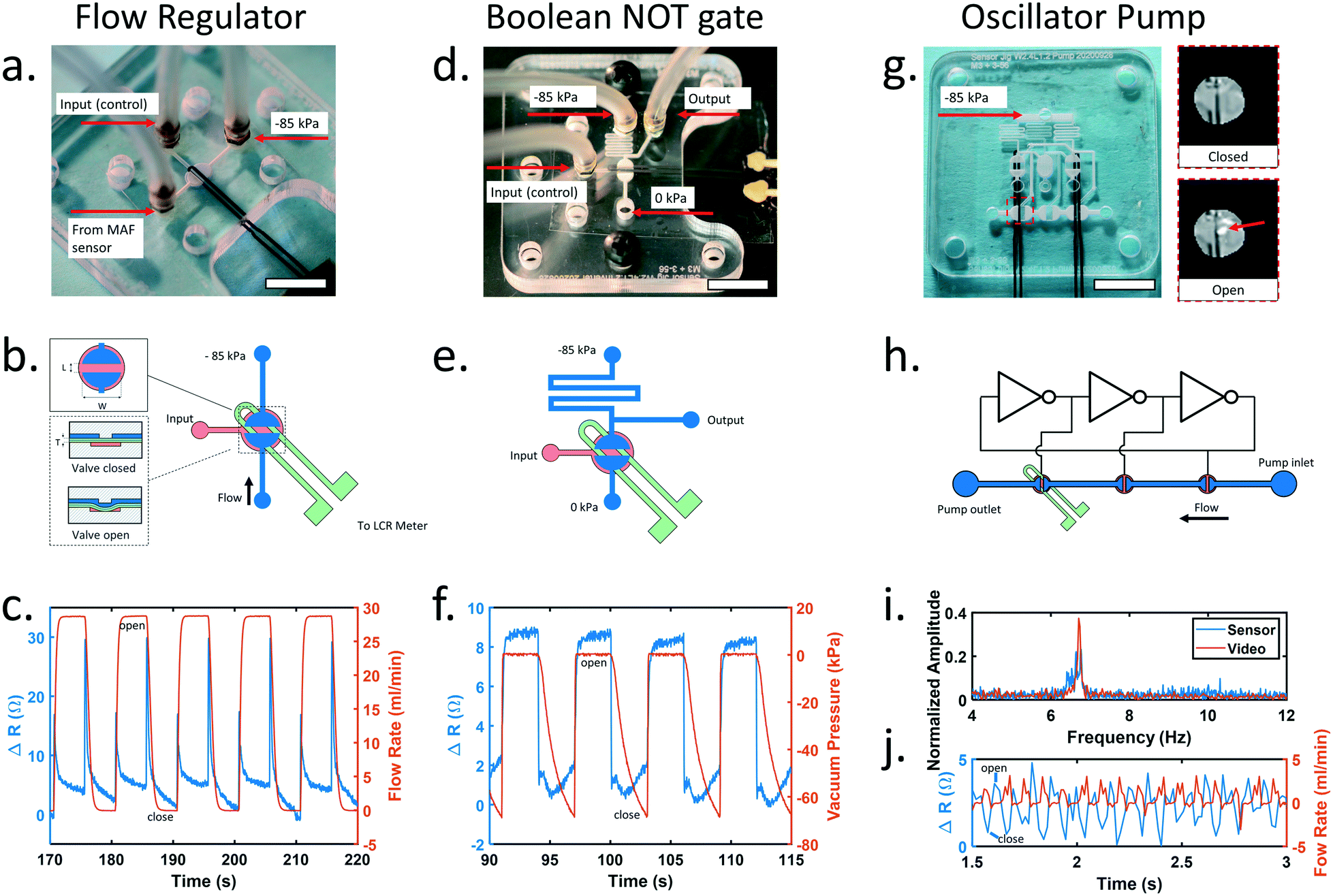 | ||
| Fig. 3 (a) Sensor integrated into an elastomeric membrane valve for control of reagent flow. (b) Valve construction details. Close up view of overhead (top inset) and cross-section of valve (bottom inset). Channels on the control and flow layers are shown in red and blue, respectively. Sensor is embedded in the membrane shown in green. Valve seat length (L) = 1.2 mm, valve seat width (W) = 2.4 mm, membrane thickness (T) = 0.6 mm. (c) Sensor resistance increases when the valve is opened or closed. (d) Sensor integrated into a microfluidic inverter logic gate for microfluidic computing. (e) Inverter gate construction details. Channels on the control and flow layers are shown in red and blue, respectively. Sensor placement shown in green. (f) Comparison of sensor resistance and inverter output over time. (g) Photo of microfluidic oscillator pump with integrated sensor. Light reflected from a single valve was used for high speed video analysis (inset). Only the sensor on the left is used. (h) Schematic of peristaltic pump controlled by integrated ring oscillator circuit. The sensor was placed under the final pump valve to detect opening and closing. (i) A comparison of sensor data and high-speed video for monitoring oscillation frequency shows matching peaks at 6.71 Hz. (j) Flow rate from the peristaltic pump measured using external hot wire anemometer and corresponding sensor measurements from the final valve in the pump. All scale bars are 1 cm. | ||
Normally closed elastomeric membrane valves can also be used to create digital logic gates that are well suited for building integrated microfluidic control circuitry.9 Therefore, we next investigated the ability of the integrated piezoresistive sensor to measure the state of a valve configured as a microfluidic inverter gate. This circuit adds a pull-up resistor before the vacuum connection to the valve and an output connection upstream of the resistor to produce a digital pressure output signal that is the inverse of the input signal. The sensor reported an increase in resistance of approximately 6 ohms when the valve was opened and returned to baseline when the valve was closed, providing a clear electronic signal that corresponded to changes in the pneumatic output of the inverter gate.
Finally, to create a simple integrated microfluidic control circuit, an oscillator pump9 was constructed consisting of three identical inverter gates connected in a ring and three liquid handling valves, each connected to the output of an inverter gate (Fig. 3g). When a constant vacuum pressure was applied to the oscillator, the pressure sequence generated by each inverter opened and closed the pump valves to create a peristaltic pumping action. The piezoresistive sensor was placed under the final valve in the pump while high speed video imaging was used to monitor the incident light reflected when the valve membrane was pulled open (Fig. 3g inset). The oscillation frequency measured by the sensor agreed well with the measurements acquired using high speed video imaging, and the sensor was able to accurately measure oscillation frequencies as high as 24.9 Hz, approximately the Nyquist frequency of our acquisition device (Fig. 3i and ESI† Fig. S8). Previous work has shown that the frequency of a ring oscillator can be tuned by changing the input pressure9 and the average flow rate of an oscillator pump is dependent on the frequency.35 Using this information, the oscillation frequency can be used to calculate the average flow rate from the pump.
When placed under the final valve in the peristaltic pump (Fig. 3h), the sensor readings also aligned well with the pulsatile flow rate measurements acquired from a hot wire anemometer (Zephyr HAF, Honeywell) connected to the output of the pump (Fig. 3j). A small backflow was detected when the final pump valve opened that was mostly negated by the closing of the middle valve in the pump. Finally, a strong forward pulse occurred when the final valve closed. Monitoring the state of the final valve in the pump, the sensor can be used to indicate the instantaneous flow rate produced by the pump. A detailed explanation of the working principle of the oscillator is provided in ESI† Fig. S7.
Conclusions
We developed a soft, highly sensitive strain sensor that is able to capture 5 μm linear displacement (0.025% strain for 20 mm sensor length) in the normal and uniaxial direction and can be deformed with as little as 20 μN of force (100 Pa stress). The response time of our sensor for linear stretching is ∼50 ms. In comparison to other flexible pressure and strain sensor's response times, which ranges from ∼17 ms to ∼100 ms,16,36–38 our sensor shows relatively fast response.As an indirect flow meter, our sensor also can detect flow rate in situ as low as 6 μl min−1 with a resolution of 2 μl min−1 in our device. However, for our current set up (with only a single sensor), failure will occur if the device is clogged. This causes the pressure to build up and the sensor readings to increase, but nothing will be flowing. In future work, multiple sensors can be used such that separate measurements at each intersection of the channel can be acquired. This allows for more precise local pressure and flow monitoring. Moreover, it will allow for the detection of clogging in the channel. As the pressure increases prior to the clogged point and decreases after the clogged point, the sensors will show relatively high or low readings at different intersections.
For monitoring microfluidic valve state, our integrated sensor provides a more direct method to monitor valve actuation than existing optical monitoring methods. Currently the sensor can monitor the binary status of a single valve precisely. Due to the analog output of the sensor, it could potentially detect partially opened valve rather than binary open and closed status; however, this may require individual calibration of each sensor.
The sensor still has some drawbacks. As mentioned in the results section, hysteresis and decay of the signal affect repeatability of the sensor. With hysteresis present in our system, only the loading signal path is used for analysis. For our strain and liquid flow tests and experiments, we focused on the loading trajectory rather than unloading trajectory for consistency, particularly as the decay is less severe. For the valve experiment, we are qualitatively checking for the opening and closing of the valve along with other features of the actuation (such as spikes shown in Fig. 3). Although hysteresis still exists, it is not as critical here and can be compensated for with machine learning algorithms34 for this specific application.
Due to decay, the signal baseline varies during experiments so the starting resistance must be subtracted to zero the baseline for different experiments. Several attempts have been made to minimize hysteresis and decay. In one case, we observed that stiffer substrates demonstrate less decay; however, stiffer substrates require larger loads to deform which may decrease the detection resolution of the sensor. For some physiological applications, it may not be possible to apply larger forces. Thus, adjusting stiffness according to different applications is a potential solution to minimize hysteresis and decay. Additionally, use of other substrate materials with less intrinsic hysteresis than PDMS is possible, too.
We demonstrated the ability to integrate our soft and extremely sensitive strain sensor into microfluidic devices to provide contactless detection of pressure that can be correlated with flow rate. The sensor can also be embedded into PDMS based valves to detect the extent of valve opening in microfluidic devices. Moreover, being PDMS-based, the sensor can be easily trimmed and bonded to any other silicone-based devices via plasma treatment. The measurement results show good linear correlation between sensor reading and flow rate and pressure in the device. The sensor has a flow rate detection range from 6 microliters per minute (μL min−1) to 200 μL min−1 and a resolution of 2 μL min−1. The sensor can confirm partial or complete valve actuation under different pressures.
Because the sensor is made of PDMS, it is compatible with soft lithography and easily integrated into microfluidic chips. The stiffness of the substrate along with the sensitivity and dimensions of the sensor can be adapted to different applications. The soft and flexible substrate also makes it possible to integrate the sensor into biological applications and monitor micron-scale tissue movement. The sensors can also be readily arrayed; for example, it can be extended from one valve to multiple valves to measure several valves' status, important for large-scale microfluidic systems that require real-time feedback to control each valve.
Methods
Sensor fabrication
Fabrication of the soft strain sensors was improved for sensitivity from the previous protocol reported by Pegan et al.23 Specifically, we tuned the thickness of the metals, improved the shrinking protocol, developed a soft, customized PDMS substrate, and introduced an encapsulation layer on the sensors. Briefly, a layer of single-sided adhesive plastic shadow mask film is applied to a pre-stressed polystyrene sheet. The geometry of the mask is designed by laser etching, and then lifted off from the polystyrene sheet. Then a thickness-controlled magnetron sputter deposits 40 nm of Pt and 5 nm of Au onto the masked polystyrene sheet. The mask is removed and the polystyrene sheet is put in a convection oven set at 140 degree Celsius for 13 minutes. After the sheet shrinks under heat, the sample is placed in a 5 mM 3-mercaptopropyl trimethoxysilane (MPTMS) ethanol solution for 2 hours. After rinsing away the excess MPTMS, the dried sample is covered with polydimethylsiloxane (PDMS), which has a mass ratio of 1:20:4.2 cure to base to dimethyl silicone fluid (PMX 200), and spin-coated at 800 RPM for 35 seconds. The sample is placed in vacuum to degas and is then cured at 60 °C overnight. The PDMS and the functional metal thin film is lifted off from the polystyrene by submerging the sample in a heated acetone bath. The PDMS and bonded metal thin film is further cleaned by additional acetone and toluene rinsing. In order to make the metal film electrically isolated from the environment, another layer of PDMS with the same composition as above is spun on the other side at 1000 RPM for 35 seconds. The sample is placed at room temperature for at least 48 hours to cure. After curing, the final sensor geometry is designed and laser etched through. The pad area of the sensor is sandwiched by two pieces of acrylic to reduce any potential movement to the pad and connection area. The 28-gauge silicone wires are connected to the pad with silver conductive epoxy (M.G. Chemical Ltd).
5 μm resolution benchtop setup
A Zaber linear actuator (Zaber Technologies Inc) is mounted onto a custom acrylic stage, and the entire system is placed within a custom acrylic box to prevent any possible environmental air flow that might affect the signal acquisition. The stage contains two parts: one part is stationary; the other part is able to slide on a track uniaxially. The driving side of the linear actuator is connected to the moving part of the stage. The pad side of the sensor is mounted on the stationary side of the stage while the other side of the sensor is clamped onto the moving portion of the stage. A precision LCR meter (Keysight Technologies E4980AL) is used to acquire resistance data of the sensor. A Labview based program is used to control movement of the stage and collect stage position data from the linear actuator and sensor resistance data from the LCR meter. The linear actuator applies 6 consecutive groups of micro-cycles of 5 μm, and each group contains 300 cycles. Then the entire process is repeated at different frequencies.Pressure sensitivity test
A 3 mm × 15 mm × 1.5 mm (w × l × h) acrylic piece is place over the sensor trace area directly and a metal probe attached to a force gauge (Mark 10 M5-025). The force gauge is mounted on the test stand (Mark 10 ESM 303) and moves down at 20 μm s−1 speed until in contact with the acrylic piece. The test is repeated 5 times.Channel and device dimension and assembly
The microfluidic device contains two parts: channel and sensor. The channel is made with a positive mold on a piece of PDMS (Young's modulus ∼2.6 MPa (ref. 39)), and has a cross-sectional dimension of 50 μm × 150 μm. The total length of the channel is 241.7 mm. For flow rates from 1 μl min−1 to 200 μl min−1, the Reynolds number remains smaller than 40. Thus, the working range is always stable laminar flow, and there is no noise due to turbulence.The thin film based piezoresistive sensor consists of two layers of PDMS with customized stiffness (Young's modulus ∼250 KPa) and one layer of wrinkled bimetallic thin film (platinum and gold). The total thickness of the layer is ∼100 μm. The metal film is sandwiched and firmly bonded in between PDMS layers to stay insulated and prevent from wearing and scratching. The polymer layers and wrinkled metal film will deform under stretching or compression; due to the brittle wrinkled structure of the metal film, micro-cracks will form. As more and larger cracks form on the metal film, the electrical resistance increases.
The sensor is directly embedded at the bottom of the chip and serves as the base of the channel. The pressure required to drive fluid flow deforms the channel. As the upper and side walls of the channel are about 10-fold stiffer than the bottom sensor wall, most of the deformation will occur on the sensor surface. The electrical resistance of the sensor increases due to the deformation described above.
Microfluidic device fabrication
The microfluidic device comprises two parts: sensor and channel. The sensor part follows the same procedure as regular sensor fabrication until curing of the encapsulation layer. After curing, the sensor is ready for plasma treatment. The channel device is fabricated through a traditional replica molding process (detailed flow chart is shown in ESI† Fig. S6). The positive mold is created by applying a layer of single-sided adhesive plastic film (Frisket Film from Grafix Art) on a piece of acrylic base. The shape of the channel is designed by laser etching the outline of the channel geometry. Excess plastic film outside the channel geometry is removed after laser etching. An acrylic well is adhered to the base to create a mold. 10:1 base to cure ratio of PDMS is poured into the mold, degassed for 20 minutes, and cured for 2 hours under 60 °C. The PDMS channel device is removed from the positive mold and a biopsy punch is used to create an inlet and outlet. After cleaning both device and sensor with tape, the bottom side of the sensor and channel side of the device are placed in the plasma machine (Plasma Etch) and treated for 3 minutes. Then the sensor and device are placed with treated sides against each other and cured at 60 °C for over 2 hours for stronger bonding.
Microfluidic flow rate measurement
The outlet of the microfluidic chip is connected to a plastic pipeline and open to air. The inlet of the microfluidic chip is connected to a 3 ml syringe and controlled by a syringe pump. The syringe pump is programmed to deliver a specific flow rate to perform relevant working range, resolution, accuracy, repeatability and leaking tests. An inline pressure transducer (Omega PX 409) is connected to the syringe outlet via a T-shaped connector. A precision LCR meter (Keysight Technologies) is used to acquire sensor resistance data.Valve integration
Microfluidic valves and digital logic circuits were fabricated similarly to previous works.9 Microfluidic channels were machined into sheets of PMMA (polymethyl methacrylate) using a CO2 laser (VLS 2.3, Universal Laser Systems) and devices were assembled by aligning and sandwiching the channel layers (channel has a width of 400 μm and depth of 400 μm, resistor has a width of 200 μm and depth of 200 μm) around a piece of sensor-embedded PDMS (∼600 μm thickness). The sensor was situated directly over the valve. For the flow control valve, a constant vacuum pressure of −85 kPa was applied to one side of the flow layer while a mass air flow meter (Zephyr HAF, Honeywell) was connected to the other side through 150 cm of 0.02′′ ID Tygon microbore tubing. The valve was switched on and off with a period of 10 s and a control pressure of −85 kPa delivered via a computer-controlled miniature solenoid valve (S10, Pneumadyne, Plymouth, MN) while air flow measurements were acquired at a frequency of 90 Hz. Inverter gates were constructed similarly, leaving the input to the inverter open to room air and adding a pressure sensor (PX139, Omega) to the output of the gate. Pressure measurements were acquired at a frequency of 50 Hz. The oscillator pump consisted of a ring oscillator formed from three identical inverter gates connected in a ring and three liquid handling valves each connected to the output of an inverter. The flow rate of air from the peristaltic pump was measured by a hot wire anemometer (Zephyr HAF, Honeywell) connected to the output of the pump while images of the incident light reflected from a pump valve were acquired at 240 Hz by a camera (iPhone Xr, Apple Computer).The average pixel intensity of a region of interest over the valve was extracted and processed with a custom program written using OpenCV.40Conflicts of interest
This work was funded in part by Novoheart Holdings. E. Lee, K. Costa and M. Khine hold equity in NovoHeart Holdings. K. Costa receives financial compensation as the Chief Scientific Officer of the company. Research conducted in this study could potentially affect the value of Novoheart. COI has been disclosed to Oversight Committee at UC Irvine and at Icahn School of Medicine at Mount Sinai.Acknowledgements
The authors would like to thank Lancy Lin for graciously taking the SEM images for Fig. 1a. Research reported in this publication was supported in part by the National Institute Of General Medical Sciences of the National Institutes of Health under award number R01GM134418. The content is solely the responsibility of the authors and does not necessarily represent the official views of the National Institutes of Health.Notes and references
- G. M. Whitesides, Nature, 2006, 442, 368–373 CrossRef CAS.
- Z. Han, W. Li, Y. Huang and B. Zheng, Anal. Chem., 2009, 81, 5840–5845 CrossRef CAS.
- S. Elizabeth Hulme, S. S. Shevkoplyas and G. M. Whitesides, Lab Chip, 2009, 9, 79–86 RSC.
- A. Buchenauer, M. C. Hofmann, M. Funke, J. Büchs, W. Mokwa and U. Schnakenberg, Biosens. Bioelectron., 2009, 24, 1411–1416 CrossRef CAS.
- K. C. Clause, L. J. Liu and K. Tobita, Cell Commun. Adhes., 2010, 17, 48–54 CrossRef.
- S. S. Massenburg, E. Amstad and D. A. Weitz, Microfluid. Nanofluid., 2016, 20, 94 CrossRef.
- M. A. Unger, Science, 2000, 288, 113–116 CrossRef CAS.
- E. C. Jensen, W. H. Grover and R. A. Mathies, J. Microelectromech. Syst., 2007, 16, 1378–1385 Search PubMed.
- P. N. Duncan, T. V. Nguyen and E. E. Hui, Proc. Natl. Acad. Sci., 2013, 110, 18104–18109 CrossRef CAS.
- X. Wang, B. Li, O. L. Russo, H. T. Roman, K. K. Chin and K. R. Farmer, Microelectron. J., 2006, 37, 50–56 CrossRef.
- S. Poeggel, D. Tosi, D. Duraibabu, G. Leen, D. McGrath and E. Lewis, Sensors, 2015, 15, 17115–17148 CrossRef.
- A. Orth, E. Schonbrun and K. B. Crozier, Lab Chip, 2011, 11, 3810 RSC.
- M. Runowski, P. Woźny, N. Stopikowska, Q. Guo and S. Lis, ACS Appl. Mater. Interfaces, 2019, 11, 4131–4138 CrossRef CAS.
- V. Lien and F. Vollmer, Lab Chip, 2007, 7, 1352 RSC.
- L. Tang, J. Liu, W. Hong, T. Wang, X. Wang, X. Chen, B. Yang and C. Yang, in 2017 IEEE 30th International Conference on Micro Electro Mechanical Systems (MEMS), IEEE, 2017, pp. 1300–1303 Search PubMed.
- W. Liu, N. Liu, Y. Yue, J. Rao, F. Cheng, J. Su, Z. Liu and Y. Gao, Small, 2018, 14, 1704149 CrossRef.
- D. J. Lipomi, M. Vosgueritchian, B. C. K. Tee, S. L. Hellstrom, J. A. Lee, C. H. Fox and Z. Bao, Nat. Nanotechnol., 2011, 6, 788–792 CrossRef CAS.
- Y. Zhang, R. Howver, B. Gogoi and N. Yazdi, in 2011 16th International Solid-State Sensors, Actuators and Microsystems Conference, IEEE, 2011, pp. 112–115 Search PubMed.
- J. Lee, M. Lim, J. Yoon, M. S. Kim, B. Choi, D. M. Kim, D. H. Kim, I. Park and S.-J. Choi, ACS Appl. Mater. Interfaces, 2017, 9, 26279–26285 CrossRef CAS.
- Y.-Q. Li, P. Huang, W.-B. Zhu, S.-Y. Fu, N. Hu and K. Liao, Sci. Rep., 2017, 7, 45013 CrossRef CAS.
- D.-Y. Wang, L.-Q. Tao, Y. Liu, T.-Y. Zhang, Y. Pang, Q. Wang, S. Jiang, Y. Yang and T.-L. Ren, Nanoscale, 2016, 8, 20090–20095 RSC.
- G. Shi, S. E. Lowe, A. J. T. Teo, T. K. Dinh, S. H. Tan, J. Qin, Y. Zhang, Y. L. Zhong and H. Zhao, Appl. Mater. Today, 2019, 16, 482–492 CrossRef.
- J. D. Pegan, J. Zhang, M. Chu, T. Nguyen, S.-J. Park, A. Paul, J. Kim, M. Bachman and M. Khine, Nanoscale, 2016, 8, 17295–17303 RSC.
- L. Wang, M. Zhang, M. Yang, W. Zhu, J. Wu, X. Gong and W. Wen, Biomicrofluidics, 2009, 3, 034105 CrossRef.
- A. Grosberg, P. W. Alford, M. L. McCain and K. K. Parker, Lab Chip, 2011, 11, 4165 RSC.
- J. U. Lind, T. A. Busbee, A. D. Valentine, F. S. Pasqualini, H. Yuan, M. Yadid, S.-J. Park, A. Kotikian, A. P. Nesmith, P. H. Campbell, J. J. Vlassak, J. A. Lewis and K. K. Parker, Nat. Mater., 2017, 16, 303–308 CrossRef CAS.
- A. Czirok, D. G. Isai, E. Kosa, S. Rajasingh, W. Kinsey, Z. Neufeld and J. Rajasingh, Sci. Rep., 2017, 7, 10404 CrossRef.
- A. Baldwin, T. Hudson and E. Meng, in 2018 IEEE Micro Electro Mechanical Systems (MEMS), IEEE, 2018, pp. 361–364 Search PubMed.
- M. Tang, F. Liu, J. Lei, Z. Ai, S.-L. Hong, N. Zhang and K. Liu, Microfluid. Nanofluid., 2019, 23, 118 CrossRef.
- I. Etxebarria, J. Elizalde and R. Pacios, Smart Mater. Struct., 2016, 25, 085022 CrossRef.
- J. Etxebarria, J. Berganzo, J. Elizalde, G. Llamazares, L. J. Fernández and A. Ezkerra, Sens. Actuators, B, 2016, 235, 188–196 CrossRef CAS.
- M. H. Zarifi, H. Sadabadi, S. H. Hejazi, M. Daneshmand and A. Sanati-Nezhad, Sci. Rep., 2018, 8, 139 CrossRef.
- S. P. Lacour, D. Chan, S. Wagner, T. Li and Z. Suo, Appl. Phys. Lett., 2006, 88, 204103 CrossRef.
- B. Oldfrey, R. Jackson, P. Smitham and M. Miodownik, Front. Robot. AI., 2019, 6, 27 CrossRef.
- T. Christoforidis, E. M. Werner, E. E. Hui and D. T. Eddington, Biomed. Microdevices, 2016, 18, 74 CrossRef.
- G. Ge, Y. Cai, Q. Dong, Y. Zhang, J. Shao, W. Huang and X. Dong, Nanoscale, 2018, 10, 10033–10040 RSC.
- S. Gong, W. Schwalb, Y. Wang, Y. Chen, Y. Tang, J. Si, B. Shirinzadeh and W. Cheng, Nat. Commun., 2014, 5, 3132 CrossRef.
- S. Lee, A. Reuveny, J. Reeder, S. Lee, H. Jin, Q. Liu, T. Yokota, T. Sekitani, T. Isoyama, Y. Abe, Z. Suo and T. Someya, Nat. Nanotechnol., 2016, 11, 472–478 CrossRef CAS.
- Z. Wang, A. A. Volinsky and N. D. Gallant, J. Appl. Polym. Sci., 2014, 131, 22 CrossRef.
- G. Bradski, Dr Dobbs J. Softw. Tools, 2000, 120, 122–125 Search PubMed.
Footnote |
| † Electronic supplementary information (ESI) available. See DOI: 10.1039/d0lc01046d |
| This journal is © The Royal Society of Chemistry 2021 |