Electrically active and hydrogen passivated Zn in GaAs/AlGaAs specifically distinguished during secondary ion mass spectrometry depth profiling
Received
11th August 2020
, Accepted 19th October 2020
First published on 19th October 2020
Abstract
A precise control over the depth distribution of major, minor and trace elements in a structure is crucial for practical applications of semiconductors. Thus, reliable characterization tools capable of measuring depth distribution of electrically active impurities are essential to advance currently existing growth technologies. Secondary Ion Mass Spectrometry (SIMS) is frequently used to measure depth profiles of impurity atoms; however it provides only total elemental concentration distribution. In contrast techniques capable of measuring dopant profiles typically omit information concerning electrically inactive impurities. In this work, we propose a method for obtaining quantitative profiles of both active and hydrogen-passivated (inactive) zinc in a GaAs/AlGaAs sample using Ultra Low Impact Energy SIMS (ULIE-SIMS). The key to the procedure is the ability of ULIE-SIMS to measure complex As3Zn and hydrogen signals. The zinc–arsenic signal is a marker of the active Zn profile, whereas the hydrogen signal delivers information about the hydrogen-passivated impurity profile. Annealing of the sample provides further validation of the method as the observed increase of active Zn and decrease of passivated Zn signals is associated with hydrogen escaping from the sample surface. The presented approach can potentially be used in optimization of growth processes and controlling the level of impurity activation in semiconductor materials.
1 Introduction
The presence of impurities is a key technological aspect of semiconductor based devices, both from the positive and negative point of view. Introduced atoms significantly affect their electrical properties, e.g. species incorporated into the lattice determine the type of conductivity and the doping level affects the free carrier concentration. Unintentionally introduced atoms (contamination) usually deteriorate parameters of a device. However, the doping process is far from trivial as its efficiency may be impaired by impurities which are electrically inactive. Introduced atoms may occupy sites different than substitutional sites, e.g. interstitial sites and furthermore they may form neutral complexes with atoms in the lattice, other impurities and native defects. Practical applications of semiconductor materials require precise and reproducible determination of the spatial distribution of dopants in the structure. Moreover, insight into reliable impurity profiles – both their active and inactive part - is important from the point of view of fundamental investigations and understanding of sample growth mechanisms. Many methods for obtaining impurity concentration profiles are available and commonly used, e.g. Spreading Resistance Analysis (SRA),1–6 Stripping Hall (SH),7–11 Secondary Ion Mass Spectrometry (SIMS)12–19 and Electrochemical Capacitance-Voltage profiling (ECV).20–25 Each method carries different information, and has its advantages but also limitations and drawbacks. SRA and SH provide carrier concentration distribution. Both methods are based on resistivity measurements, thus requiring knowledge of mobility. SRA relies on mobility models whereas SH yields mobility using Hall measurements.26,27 Hall measurements combined with modeling and theoretical calculations are also a valuable tool in determining factors limiting the conductivity of the samples.28,29 In contrast standard dynamic SIMS is a surface sensitive method based on the chemical composition of the samples and provides depth profiles of all impurities including active and inactive parts. The ECV profiling allows for directly obtaining the concentration profiles of all carriers present in a structure. Typically when the doping level is relatively high this approximately corresponds to the dopant concentration. Thus, ECV profiles in many cases can provide more useful information than SIMS measurements. However, in the ECV method the etch profile has to be measured after profiling which may introduce considerable error. SIMS measurements include the inactive part of introduced atoms in concentration profiles; however, there have been no reports of the separation of such an inactive impurity profile from the total impurity concentration distribution. Nonetheless SIMS measurements can be useful when all impurity atoms are ionized and the total chemical concentration approximately corresponds to the dopant concentration.30–34
Zinc is one of the most common p-type dopants in GaAs and AlGaAs.35–37 This is due to its high solubility and low ionization energy.36 Furthermore Zn precursors are easy to handle and homogeneous doping can be easily achieved.35 Zinc diffusion coefficient in GaAs is a concentration dependent function which behaves differently depending on the dominating diffusion mechanism.38–40 Zinc atoms introduced into the A(III)–B(V) lattice are electrically activated mostly by substituting at III group element sites and thus by binding with V group elements. Over the years many reports about the passivation of II-group element impurities in A(III)–B(V) materials using hydrogen have been made.41–46 In the case of the Zn atom in GaAs hydrogen in neutral complexes is bonded to arsenic in the close vicinity of the acceptor atom.41,43 Hydrogen compounds are used in the technological process of the growth of doped A(III)–B(V) type materials using the Metal–Organic Chemical Vapor Deposition (MOCVD) method. Therefore, parasitic hydrogen may appear in the sample and passivate introduced impurities. The huge advantage of standard SIMS depth profiling is its capability to measure quantitatively the distribution of hydrogen in the sample.47
Using Ultra Low Impact Energy SIMS (ULIE-SIMS) recently has contributed to the development of the capabilities of SIMS measurements. The ULIE-SIMS method allows us not only to reach subnanometer depth resolution but also to probe the chemical state of the sample during profiling.48 In our recent work we have shown the possibility of getting qualitative information about bonds present in the sample.48 In this paper we apply the ULIE SIMS method in investigations of activation and passivation of Zn in the GaAs/Al0.3Ga0.7As:Zn/GaAs structure. We propose a method for obtaining information about the active Zn profile and hydrogen passivated Zn profile in the GaAs/Al0.3Ga0.7As:Zn/GaAs structure using ULIE SIMS which may be beneficial in optimization of the growth process and controlling the level of impurity ionization.
2 Materials and methods
2.1 Sample preparation
Epitaxial layers of GaAs/Al0.3Ga0.7As doped with Zn were grown on 3-inch diameter n-type GaAs substrates with exact orientation (100). Growth by MOCVD was performed in an AIX 2800 G4 low pressure horizontal laminar flow reactor with a 12 × 3′′ configuration. This enables the creation of atomically engineered epitaxial layers of binary, ternary and quaternary III–V compound semiconductors with a wide range of doping concentrations. It is fitted with a horizontal laminar flow reactor, which ensures precise heterojunctions and unrivalled control of the deposition rates at the monolayer level. This principle coupled with the multiple rotation of substrate carriers guarantees excellent deposition homogeneity regarding layer thickness, composition and doping. Trimethylgallium (TMGa) and trimethylaluminum (TMAl) were used as III-group sources and arsine (AsH3) as the group-V source. The growth temperature was 660 °C. For p-type doping, a Diethylzinc (DEZn) precursor was used. Precise doping is realized thanks to in situ mixing of DEZn with Pd-purified hydrogen used in the epitaxial process as a carrier gas. The AlGaAs chemical composition was assessed by the photoluminescence method (PL) in mapping mode and crossed-checked by X-ray diffraction against PL. Thickness and growth rate were calibrated using SEM cross-section analysis together with in situ reflectometry. The purity of the undoped epitaxial layers was tested by measuring by the Hall method achieving the concentration level of n-type contaminations as (1–2) × 1014 atoms per cm3 whereas doped samples were investigated by means of the electrochemical capacitance–voltage technique.
2.2 ECV
The doping profile was measured using a Wafer Profiler CVP21 by Electrochemical Capacitance Voltage Profiling (ECV-Profiling, CV-Profiling). An interface to the semiconductor surface is formed by an electrolyte, which wets an area of 1 mm2 and is bound by a sealing ring. Under reverse voltage this interface acts like a Schottky-like contact, and with the usual CV technique the concentration of charge carriers in n- and p-doped semiconductors can be evaluated.49 The semiconductor is etched by pressing hole carriers against the semiconductor surface, where these holes “release” valency electrons of the atoms, so that the semiconductor atoms move into the electrolyte in the positive ionisation state (freed from their valence electrons). For the p-doped surface, voltage is used to push hole carriers to the surface. For the n-doped surface, the hole carriers are generated by illuminating the interface with UV light, whereby the Schottky-surface is operated under reverse voltage (thus then the intrinsic electric field of the surface depletion layer pushes the generated hole carriers to the surface. Fortunately for ECV etching, this “intrinsic electric depletion field”, in the case of n doped layers, has the correct polarity for this task (surface negatively doped). The doping profile of the semiconductor surface layer is evaluated by alternating measurement steps and etch steps. The entire measuring process is controlled by software so that the profile can be determined fully automatically. The electrolyte used was 0.1 M EDTA (Titriplex III) dissolved in a solution of 5% ethyl diamine in deionized water. With a fully digital measuring bridge the admittance of the depletion zone at the surface of the semiconductor is determined in the frequency range of 1-50 kHz by a 4 wire method (thus minimizing the influence of the semiconductor contact resistance, or the electrolyte resistance). An equivalent circuit diagram with consideration of series resistance and parallel resistance is used to calculate the capacitance of the surface depletion zone from this measured admittance with high accuracy and reliability. If the border of the depletion layer in the semiconductor is assumed to be sharp and the semiconductor material is assumed to be homogeneous, the measured capacitance C depends on the applied voltage V, whereas 1/C2 depends on the carrier concentration.
2.3 SIMS
In this work all SIMS measurements were performed employing a CAMECA SC Ultra instrument under ultra-high vacuum (UHV), usually of 4 × 10⁻¹⁰ mbar. The Cs+ primary beam was rastered over 150 × 150 μm2 (the analysis area was limited to 100 × 100 μm2). The positive ion detection mode was used in most experiments and thus all species were measured as CsX+ cluster ions and point-to-point normalized to Cs+ signals. The intensity of the primary beam was 5 nA and the impact energy was 150 eV. For hydrogen profiling the detection mode was switched to negative and the H− species was measured. The rest of the parameters remained the same. To increase the sensitivity titanium pre-sputtering was employed prior to the hydrogen profiling50 and the background level was reduced to 7 × 10¹⁷ atoms cm−3. Zn, H and As3Zn signals were calibrated. For the former two standard reference samples were used: clean substrate ions implanted with zinc and hydrogen, respectively.51 As3Zn signal calibration was based on ECV results: the total number of counts and hole concentration were integrated for depths 100–500 nm (surface was intentionally omitted as ECV is not reliable for a surface region) and direct proportionality between these two values was assumed. The calculation of total doses of Zn an H along with uncertainties was based on eight different measurements.
3 Results and discussion
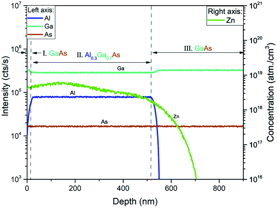
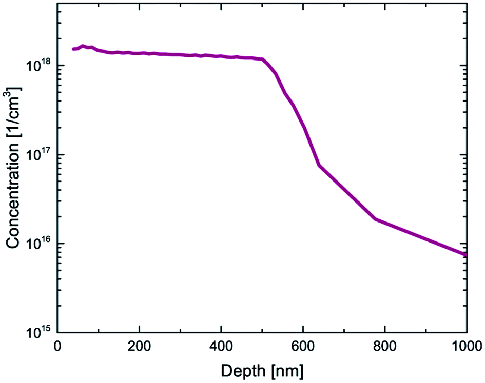
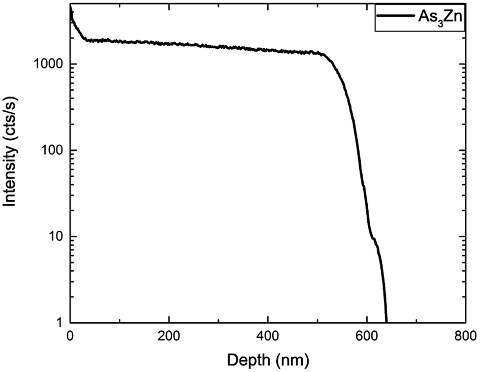
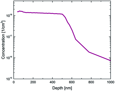
Fig. 1 shows the depth profile of the GaAs/Al0.3Ga0.7As:Zn/GaAs structure obtained by the Secondary Ion Mass Spectrometry (SIMS) technique. SIMS measurements reveal natural division into three regions depending on the content of individual components. In the first area near the surface, the intensity of Ga and As signals stays approximately constant in contrast to the concentration of aluminum which is increasing with depth. Furthermore in the third region in Fig. 1 decreasing of aluminum can be observed. Thus, the technological method of growth is burdened with inaccuracy leading to incorporation of the GaAs structure with Al atoms in the vicinity of Al0.3Ga0.7As. In the second region between (20–510) nm, the Al0.3Ga0.7As structure is clearly present on the grounds of lowering of Ga signals and establishing of constant Al, Ga, and As ratios. In the growth process only Al0.3Ga0.7As was doped with Zn atoms, however the Zn profile shows clear diffusion of impurity atoms into the third region of the sample. Zinc distribution shown in Fig. 1 is a typical diffusion profile observed for this impurity in gallium arsenide.36,52 SIMS is usually used to measure the elemental composition of the investigated sample providing its depth profile which carries information about the concentration distribution of impurity atoms (Fig. 1), whereas the electrochemical capacitance–voltage profiling technique enables obtaining the concentration of all carriers (including electrically active impurities) as a function of sample depth. The results of ECV measurements performed on the GaAs/Al0.3Ga0.7As:Zn/GaAs sample are shown in Fig. 2. For many materials a vast majority of impurity atoms are electrically active and thus the electrochemical capacitance–voltage profiling technique and secondary ion mass spectrometry measurements can be used interchangeably. In this case, however, we have found significant discrepancies between these two techniques (Fig. 1 – green curve and Fig. 2). Comparison of these curves shows that they have different shapes although the order of magnitude of the concentrations (1018 cm−3) obtained from both methods is similar. SIMS measurements globally reveal a higher concentration (up to 6 × 1018 cm−3) than ECV results (up to 2 × 1018 cm−3) which may suggest that some Zn atoms in the sample are electrically inactive. However, standard SIMS measurements do not allow a distinction between active and inactive impurities. In our previous work48 we have shown that for ultra low impact energy primary ions SIMS measurements can provide qualitative information about the chemical state of the profiled material – for such low impact energy (90–150 eV) primary ions carry too little energy to effectively break strong covalent bonds and thus the probability to sputter larger species is higher. Impurity atoms introduced in III–V type materials activate mostly by substituting at III-group element sites in the lattice, thus it can be assumed that zinc atoms are essentially electrically active when covalently bonded with arsenide. Hence it should be possible to measure dopant atom distribution by monitoring the As3Zn profile obtained with ultra low impact energy SIMS. It is important to emphasize that the rate and range of energy transfer depends on the density of the medium and can affect the measurement results. The difference between the applied impact energy (150 eV) and the As–Ga bond dissociation energy (202.5 [kJ mol−1] ≈ 2.099 [eV])53 shows that it may be possible to release very fragmented structures. Important parameters that characterize the crystal lattice are electronegativity and the atomic radius of the components. Hydrogen atoms as impurities could incorporate into the GaAs/AlGaAs structure in which some Ga atoms (136 pm) were replaced by Zn atoms (142 pm). Due to their small radius (53 pm), hydrogen atoms may be incorporated into the lattice structure and disturb its packing and increase the density. It can be hypothesized that energy supplied during SIMS measurements by cesium cations to a material with the density increased by hydrogen passivation, can cause intense fragmentation higher than in the case of less dense – unpassivated structures, which was considered based on the physical properties of the atoms – components of the structure. The results presented in Fig. 3 show that in this case the shape of the obtained profile is in a good agreement with ECV measurements (Fig. 2) confirming the validity of the performed experiment. Hence, the SIMS profile of Zn corresponds to the concentration of all impurity atoms while the As3Zn profile reveals information about the distribution of active impurity centers.
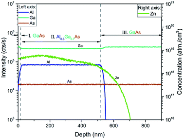 |
| | Fig. 1 Depth profile of the GaAs/Al0.3Ga0.7As:Zn/GaAs structure measured by SIMS using Cs+ primary ions of energy 150 eV. All species were measured as CsX+ cluster ions and point-to-point normalized to Cs+ signals. The quality of grown heterostructure layers is high, however visible diffusion of the nonuniform Zn profile into deeper regions of the sample occurs. | |
 |
| | Fig. 2 Carrier concentration measured by the ECV method. The electrolyte used was 0.1 M EDTA (Titriplex III) dissolved in a solution of 5% ethyl diamine in deionized water. | |
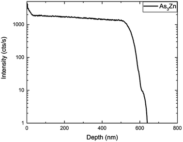 |
| | Fig. 3 Distribution of active Zn measured by SIMS using ultra low impact energy. Shape of the obtained profile is in good agreement with ECV measurements. | |
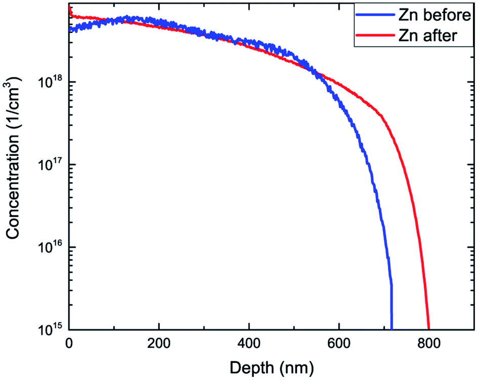
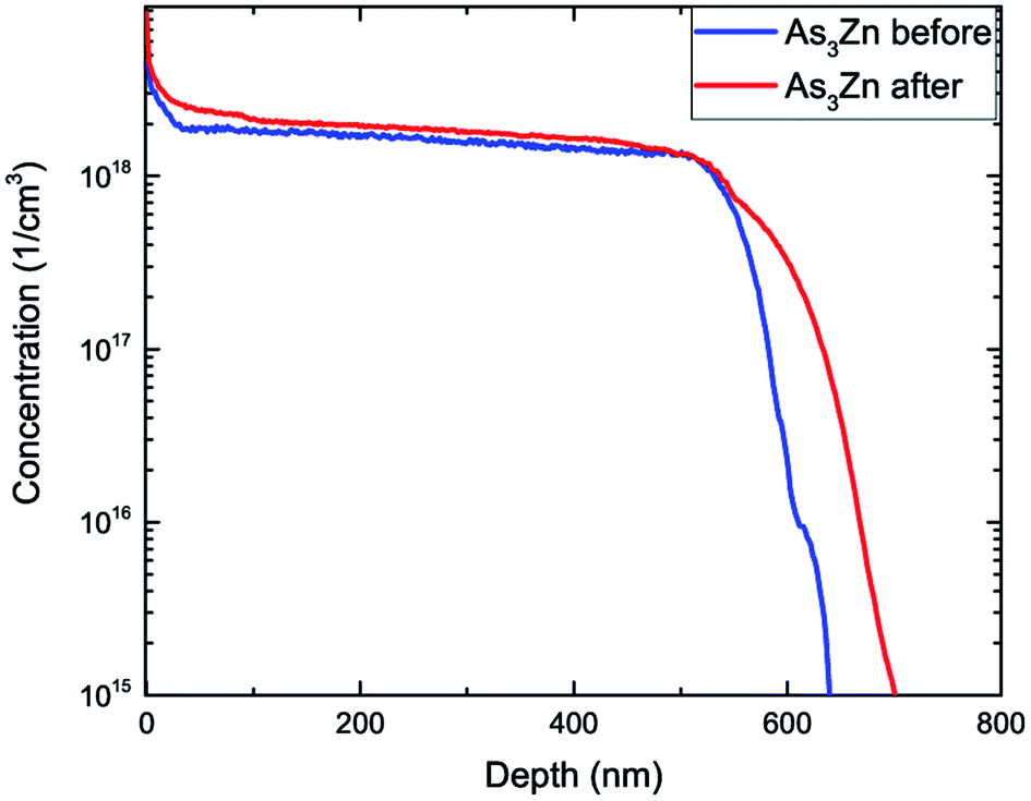
To study the effect even further we have repeated SIMS experiments for the sample annealed at 650 °C for half an hour. Changes of material properties under high temperature conditions are significant factors when considering technological procedures used in manufacturing of electronic appliances. Comparison of the concentration distribution of Zn before and after annealing (Fig. 4) shows diffusion of Zn manifested by its increased concentration in the vicinity of the exterior surface and towards the GaAs substrate. The total concentration (dose) of Zn atoms before and after annealing is in excellent agreement with each other reaching (2.267 ± 0.012) × 1015 at. per cm2 and (2.270 ± 0.012) × 1015 at. per cm,2 respectively. Fig. 5 shows the concentration distribution registered for As3Zn profiles using ultra low impact energy SIMS before and after the annealing process. The number of As3Zn species has increased after annealing which is especially evident in the area neighboring the surface but also noticeable for larger depths. Hence the concentration of active Zn is higher after exposure to high temperatures in contrast to the total Zn profile which has maintained a constant dose after annealing. The dose of active Zn before annealing reaches only 40% of the total Zn dose and increases to 47% of its value after the annealing process. Despite the increase of the dopant concentration, a large number of Zn atoms remain inactive. Hence, the concentration of total Zn present in the sample C(Zntotal) consists of two parts – electrically active and inactive zinc. A well-recognized reason for the passivation of the zinc dopant in III–V type materials given in the literature is hydrogenation.41–46 Thus, inactive contribution to C(Zntotal) may be described as the sum of concentrations of hydrogen passivated atoms C(ZnHpassivated) and those remaining inactive for other reasons C(Zninactive):
| C(Zntotal) = C(Znactive) + C(ZnHpassivated) + C(Zninactive) |
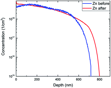 |
| | Fig. 4 Comparison of the concentration of Zn obtained by SIMS before and after annealing. | |
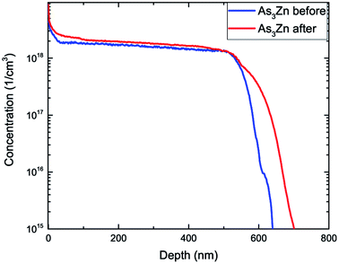 |
| | Fig. 5 Comparison of the concentration of Zn obtained by SIMS before and after annealing. | |
The decrease of active Zn under hydrogen-rich conditions is due to the formation of neutral Zn–H complexes. Therefore it may be assumed that the concentration of passivated Zn is proportional to the concentration of hydrogen:
where
α is the proportionality coefficient. Hence hydrogen profiles may provide qualitative information about the distribution of passivated Zn.
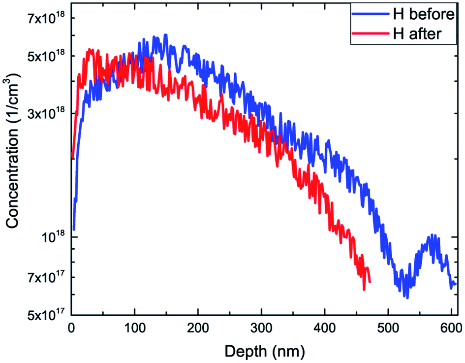
Fig. 6 shows hydrogen profiles measured by SIMS before and after annealing. The dose of hydrogen decreases after exposure to high temperatures to 62% of its initial value, which is due to escaping of H atoms from the surface. Thus, fewer hydrogen atoms have been involved in forming neutralized complexes with impurities and consequently the dose of active Zn has increased (
Fig. 5).
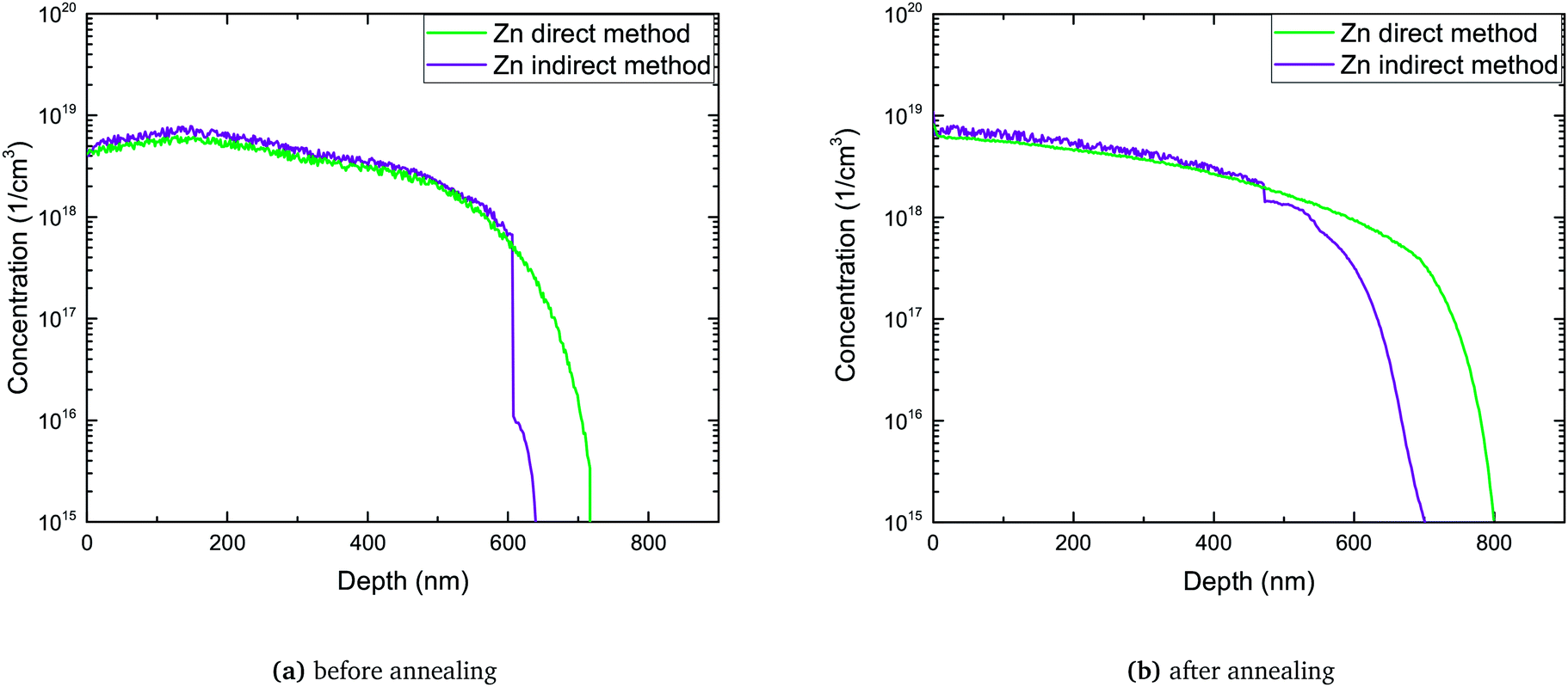
Fig. 7a and b presents a comparison of Zn profiles obtained directly by SIMS measurements and indirectly by adding concentrations of electrically active and hydrogen passivated Zn. In order to qualitatively estimate the compatibility of both profiles the proportionality coefficient
α = 1 was taken to attain the Zn
Hpassivated concentration distribution. For depths smaller than 600 nm shapes of curves in
Fig. 7a are in good agreement suggesting that presence of hydrogen is the main reason for Zn passivation in this area. Furthermore, other factors which may suppress the concentration of active Zn such as native defects have almost a negligible influence in the profile appearance. The intensity of the profile obtained by summation is higher than the directly measured Zn profile in consequence of only qualitative estimation of the hydrogen passivated Zn concentration.
Fig. 7b shows the comparison of Zn
total profiles resulting from both methods obtained after the annealing process. The compatibility of the profiles has been maintained on a high level affirming the validity of the summation approach. Not all hydrogen atoms have been involved in the passivation process thus, to obtain a more quantitative picture, an appropriate value of coefficient
α < 1 should be included. However comparison of hydrogen and active Zn after annealing measurements reveals that the decrease of hydrogen dose and the increase of the active Zn dose are of the same order of magnitude (0.35 × 10
15 at. per cm
2 and 0.16 × 10
15 at. per cm
2 respectively) which indicates that a significant number of escaping hydrogen atoms originated from neutral hydrogen–zinc complexes. In deeper regions Zn profiles in
Fig. 7a (>600 nm) and
Fig. 7b (>450 nm) exhibit considerable discrepancies; however, this can be explained by much lower detection limits of the indirect method.
 |
| | Fig. 6 Hydrogen profiles measured by SIMS before and after annealing. | |
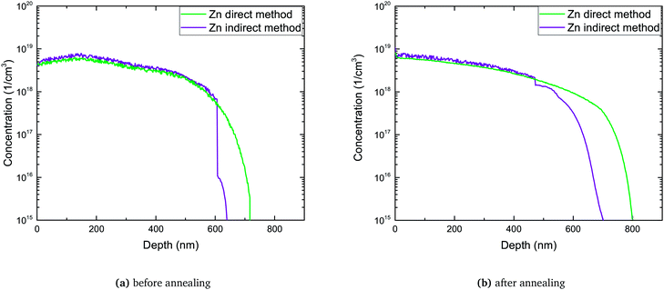 |
| | Fig. 7 Comparison of the total Zn profile measured directly by SIMS with sum of passivated and active Zn profiles (indirect method). | |
4 Conclusions
We have shown that ultra low impact energy SIMS can be a valid source of information about activation and passivation of Zn in III–V type materials. Using such a low primary ion beam energy guarantees sub-nanometer depth resolution hence the method can be applied to ultra thin films. The presented approach allows us to make a distinction between active and inactive impurity atoms extending standard capabilities of the Secondary Ion Mass Spectrometry method. An important conclusion obtained from SIMS zinc profiles is that a significant amount of Zn is electrically inactive. Furthermore, hydrogen passivation is clearly the most significant factor suppressing Zn activation in the investigated sample. By engaging the indirect method based on SIMS measurements of the hydrogen profile it is possible to gain qualitative information about passivated Zn distribution. The applied technique can be a valuable tool for the depth profiling of doped semiconductor materials.
Conflicts of interest
There are no conflicts to declare.
Acknowledgements
This work was supported by the National Science Centre (NCN) within the SONATA14 2018/31/D/ST5/00399 project and by the National Center for Research and Development within the Scieżka dla Mazowsza, MAZOWSZE/0032/19-00 project.
Notes and references
- R. G. Mazur and D. H. Dickey, J. Electrochem. Soc., 1966, 113, 255 CrossRef CAS.
- D. D'Avanzo, R. Rung, A. Gat and R. Dutton, J. Electrochem. Soc., 1978, 125, 1170–1176 CrossRef.
- R. Mazur, ACS Symp. Ser. Am. Chem. Soc., 1986, 295, 34–48 CAS.
- T. Clarysse and W. Vandervorst, J. Vac. Sci. Technol. B, 1994, 12, 290–297 CrossRef CAS.
- L. Tan, L. Tan, M. Leong, R. Mazur and C. Ye, J. Vac. Sci. Technol. B, 2002, 20, 483–487 CrossRef CAS.
- T. Clarysse, D. Vanhaeren, I. Hoflijk and W. Vandervorst, Mater. Sci. Eng., R, 2004, 47, 123–206 CrossRef.
- S. R. Blight, R. E. Nicholls, S. P. S. Sangha, P. B. Kirby, L. Teale, S. P. Hiscock and C. P. Stewart, J. Phys. E, 1988, 21, 470–479 CrossRef CAS.
-
M. Polignano and G. Queirolo, Chapter 6 Studies of the Stripping Hall Effect in Ion-Implanted Silicon, Elsevier, 1997, vol. 45, pp. 165–194 Search PubMed.
- T. Alzanki, R. Gwilliam, N. Emerson, Z. Tabatabaian, C. Jeynes and B. J. Sealy, Semicond. Sci. Technol., 2004, 19, 728–732 CrossRef CAS.
- N. Bennett, N. Cowern, A. Smith, M. Kah, R. Gwilliam, B. Sealy, T. Noakes, P. Bailey, D. Giubertoni and M. Bersani, Mater. Sci. Eng., B, 2008, 154–155, 229–233 CrossRef CAS.
- R. Daubriac, E. Scheid, H. Rizk, R. Monflier, S. Joblot, R. Beneyton, P. A. Alba, S. Kerdilès and F. Cristiano, Beilstein J. Nanotechnol., 2018, 9, 1926–1939 CrossRef CAS.
-
G. D. T. Spiller and J. R. Davis, Quantification of SIMS Dopant Profiles in High-Dose Oxygen-Implanted Silicon, Using a Simple Two-Matrix Model, Springer Berlin Heidelberg, Berlin, Heidelberg, 1986, pp. 334–336 Search PubMed.
- M. Takase and B. Mizuno, Nucl. Instrum. Methods Phys. Res., Sect. B, 1997, 121, 288–290 CrossRef CAS.
- P. Kröner, H. Baumeister, J. Rieger, E. Veuhoff, M. Popp and H. Heinecke, J. Cryst. Growth, 1998, 195, 660–667 CrossRef.
- H. Smith, B. Tsao and J. Scofield, Mater. Sci. Forum, 2006, 527–529, 629–632 CAS.
- S. Hong, Y.-S. Kim, W. Lee, Y. Kim, J. Song, J. Jang, j. h. Park, S.-H. Choi and K. Kim, Nanotechnology, 2011, 22, 425203 CrossRef.
- R. Wilson and J. Zavada, Mater. Sci. Eng., R, 2012, 73, 101–128 CrossRef.
- Y. Arakawa, K. Ueno, A. Kobayashi, J. Ohta and H. Fujioka, APL Mater., 2016, 4, 086103 CrossRef.
- G. Kartopu, B. Williams, V. Zardetto, A. Gürlek, A. Clayton, S. Jones, W. Kessels, M. Creatore and S. Irvine, Data Brief., 2019, 22, 218–221 CrossRef CAS.
- T. Ratcliff, A. Shalav, K. C. Fong, R. Elliman and A. Blakers, Energy Procedia, 2014, 55, 272–279 CrossRef CAS.
- G. Yakovlev and V. Zubkov, J. Phys.: Conf. Ser., 2018, 993, 012038 CrossRef.
- K. M. Yu and M. Ridgway, Nucl. Instrum. Methods Phys. Res., Sect. B, 2000, 168, 65–71 CrossRef CAS.
- M. Udhayasankar, J. Kumar and P. Ramasamy, J. Cryst. Growth, 2004, 268, 389–395 CrossRef CAS.
- D. S. Frolov, G. E. Yakovlev and V. I. Zubkov, Semiconductors, 2019, 53, 268–272 CrossRef CAS.
- P. Modak, M. Kumar Hudait, S. Hardikar and S. Krupanidhi, J. Cryst. Growth, 1998, 193, 501–509 CrossRef CAS.
- N. Bennett, A. Smith, B. Colombeau, R. Gwilliam, N. Cowern and B. Sealy, J. Mater. Sci. Eng. B, 2005, 124–125, 305–309 CrossRef.
-
S. Werner, U. Belledin, A. Kimmerle, A. Fallisch, A. Wolf and D. Biro, 25th European Photovoltaic Solar Energy Conference and Exhibition, 2010, pp. 1942–1947 Search PubMed.
- J. E. N. Swallow, B. A. D. Williamson, T. J. Whittles, M. Birkett, T. J. Featherstone, N. Peng, A. Abbott, M. Farnworth, K. J. Cheetham, P. Warren, D. O. Scanlon, V. R. Dhanak and T. D. Veal, Adv. Funct. Mater., 2018, 28, 1701900 CrossRef.
- T. Slupinski, M. Molas and J. Papierska, Acta Phys. Pol., A, 2009, 116(5), 979–982 CrossRef CAS.
-
M. Heinrich, H. Hidayat, Z. Hameiri, B. Hoex and A. Aberle, Proc of 27th EU-PVSEC, 2012, vol. 27, pp. 1285–1288 Search PubMed.
- A. Lanterne, T. Desrues, C. Lorfeuvre, M. Coig, F. Torregrosa, F. Milési, L. Roux and S. Dubois, Prog. Photovoltaics, 2019, 27, 1081–1091 CAS.
- P. Goyal, E. Urrejola, J. Hong and A. Madec, Energy Procedia, 2015, 77, 470–477 CrossRef CAS.
- Z. Essa, N. Taleb, B. Sermage, C. Broussillou, B. Bazer-Bachi and M. Quillec, EPJ Photovoltaics, 2018, 9, 5 CrossRef.
- A. Bentzen, A. Holt, J. S. Christensen and B. G. Svensson, J. Appl. Phys., 2006, 99, 064502 CrossRef.
- M. Hudait, P. Modak, S. Hardikar and S. Krupanidhi, J. Appl. Phys., 1997, 82, 4931–4937 CrossRef CAS.
- H. Bracht and S. Brotzmann, Phys. Rev. B: Condens. Matter Mater. Phys., 2005, 71, 115216 CrossRef.
- S. Yu, T. Y. Tan and U. Gösele, J. Appl. Phys., 1991, 69, 3547–3565 CrossRef CAS.
- B. Tuck and M. A. H. Kadhim, J. Mater. Sci., 1972, 7, 585–591 CrossRef CAS.
- S. Reynolds, D. W. Vook and J. F. Gibbons, J. Appl. Phys., 1988, 63, 1052–1059 CrossRef CAS.
- H. Ye, L. Tang and Q. Ni, J. Mater. Sci. Eng. B, 2015, 197, 1–4 CrossRef CAS.
- B. Pajot, A. Jalil, J. Chevallier and R. Azoulay, Semicond. Sci. Technol., 1987, 2, 305–307 CrossRef CAS.
- J. Chevallier, A. Jalil, B. Theys, J. C. Pesant, M. Aucouturier, B. Rose and A. Mircea, Semicond. Sci. Technol., 1989, 4, 87–90 CrossRef CAS.
- R. Rahbi, B. Pajot, J. Chevallier, A. Marbeuf, R. C. Logan and M. Gavand, J. Appl. Phys., 1993, 73, 1723–1731 CrossRef CAS.
- A. Ishibashi, M. Mannoh and K. Ohnaka, J. Cryst. Growth, 1994, 145, 414–419 CrossRef CAS.
- N. M. Johnson, R. D. Burnham, R. A. Street and R. L. Thornton, Phys. Rev. B, 1986, 33, 1102–1105 CrossRef CAS.
-
M. D. Mccluskey and E. E. Haller, Chapter 9 - Hydrogen in III-V and II-VI Semiconductors, Elsevier, 1999, vol. 61, pp. 373–440 Search PubMed.
- C. W. Magee and E. Botnick, J. Vac. Sci. Technol., 1981, 19, 47–52 CrossRef CAS.
- P. P. Michałowski, J. Anal. At. Spectrom., 2019, 34, 1954–1956 RSC.
- P. Blood, Semicond. Sci. Technol., 1986, 1, 7–27 CrossRef CAS.
- P. P. Michałowski, J. Anal. At. Spectrom., 2020, 35, 1047–1050 RSC.
- D. P. Leta and G. H. Morrison, Anal. Chem., 1980, 52, 514–519 CrossRef CAS.
- M. P. Chase, M. D. Deal and J. D. Plummer, J. Appl. Phys., 1997, 81, 1670–1676 CrossRef.
-
Y. R. Luo, Comprehensive handbook of chemical bond energies, CRC Press, Boca Raton, 2007 Search PubMed.
|
| This journal is © The Royal Society of Chemistry 2021 |
Click here to see how this site uses Cookies. View our privacy policy here. 
 *ab,
Walery
Kolkowski
c,
Iwona
Pasternak
cd,
Włodzimierz
Strupiński
cd,
Sylwia
Kozdra
*ab,
Walery
Kolkowski
c,
Iwona
Pasternak
cd,
Włodzimierz
Strupiński
cd,
Sylwia
Kozdra