 Open Access Article
 This Open Access Article is licensed under a
 Creative Commons Attribution 3.0 Unported Licence
Stability and universal encapsulation of epitaxial Xenes
Alessandro
Molle
 *a,
Gabriele
Faraone
ab,
Alessio
Lamperti
a,
Daniele
Chiappe†
a,
Eugenio
Cinquanta
c,
Christian
Martella
a,
Emiliano
Bonera
b,
Emilio
Scalise
b and
Carlo
Grazianetti
a
*a,
Gabriele
Faraone
ab,
Alessio
Lamperti
a,
Daniele
Chiappe†
a,
Eugenio
Cinquanta
c,
Christian
Martella
a,
Emiliano
Bonera
b,
Emilio
Scalise
b and
Carlo
Grazianetti
a
aCNR-IMM, Unit of Agrate Brianza, Via C. Olivetti 2, 20864 Agrate Brianza, Italy. E-mail: alessandro.molle@cnr.it
bDipartimento di Scienza dei Materiali, Università degli Studi Milano-Bicocca, Via R. Cozzi 55, 20125, Milano, Italy
cCNR-IFN, Piazza Leonardo da Vinci 32, 20133 Milano, Italy
First published on 30th December 2019
Abstract
In the realm of two-dimensional material frameworks, single-element graphene-like lattices, known as Xenes, pose several issues concerning their environmental stability, with implications for their use in technology transfer to a device layout. In this Discussion, we scrutinize the chemical reactivity of epitaxial silicene, taken as a case in point, in oxygen-rich environments. The oxidation of silicene is detailed by means of a photoemission spectroscopy study upon carefully dosing molecular oxygen under vacuum and subsequent exposure to ambient conditions, showing different chemical reactivity. We therefore propose a sequential Al2O3 encapsulation of silicene as a solution to face degradation, proving its effectiveness by virtue of the interaction between silicene and a silver substrate. Based on this method, we generalize our encapsulation scheme to a large number of metal-supported Xenes by taking into account the case of epitaxial phosphorene-on-gold.
Introduction
Epitaxial Xenes are a quickly emerging reality in the realm of two-dimensional (2D) crystals beyond graphene. They were recently sorted into two generations according to the position of the constitutive element (X) in the periodic table (the first generation includes elements in the silicon group, whereas the second includes elements in the boron, nitrogen, and oxygen groups).1 Compared to other 2D players, they constitute a broad portfolio of materials with variable and configurable properties depending on the growth environment (e.g. the substrate) or the atomistic details (e.g. buckled bonding). As epitaxial materials, they are scalable and thus look promising for industrial applications. The heavier among them are also prone to hosting a 2D topological insulating state of matter.2,3 While structure and electronic properties may vary throughout the Xene generations,4,5 a common issue for all single-layer Xenes relates to stability against environmental reactivity. This is basically due to the fact that bonding in Xenes is less stable than in graphene or other layered compounds. A paradigmatic example in this respect is silicene (and silicene-like materials like germanene and stanene), where pseudo sp2 bonding is artificially induced by means of configurational constraints.6 This synthetic set-up poses several questions concerning the stability of silicene and similar materials. For instance, is silicene prone to degradation under ambient conditions? How does silicene undergo oxidation? How to protect silicene from degradation? And how to extend such a protective process to the whole class of Xenes? In this Discussion, we elaborate on specific aspects of the chemical stability of the Xenes by reporting original data on the exposure of epitaxial silicene to a O2-rich environment in ultra-high vacuum (UHV) growth conditions. Silicene, as well as other Xenes, undergoes degradation in environmental conditions unless a protective layer is applied. Encapsulation, as opposed to passivation, aims to form a barrier to the external atmosphere without changing either the bonding or the functional properties of the Xenes. This can be a difficult task because we need the encapsulating layer to grow on top of the Xene, while having minimal interaction with it. In this respect, we state the conditions for a universal encapsulation scheme for metal-supported Xenes and support it with a preliminary ab initio model. To corroborate the universal character of the approach, we scrutinize the epitaxial phosphorene on Au(111) as a second case in point.Silicene reactivity
The oxidation of silicon constituted a milestone in integrated microelectronic circuits, enabling the ubiquitous integration of silicon. Now that silicon-based devices are approaching ultimate scaling, the oxidation of silicene, namely silicon at the 2D level, may open new technology paths of silicon exploitation in nanoelectronics. One step in this direction is to investigate how the chemical bonding in epitaxial silicene is affected by an oxygen-rich environment. We elucidate this scenario in a variable dosage experiment starting from an UHV condition and monitoring the synchrotron radiation Si 2p core-level photoemission line of epitaxial silicene-on-silver(111) with increasing O2 partial dose. Two silicene configurations were taken into account, the low-temperature mixed 4 × 4/√13 × √13 phase (Fig. 1a) and the high-temperature 2√3 × 2√3 phase (Fig. 1b), as they were proven to be the precursors for a room temperature operational field effect transistor.7 Basically, the two configurations differ in terms of their buckled bond pattern,8 as evidenced by the markedly different positioning of the E2g Raman mode as well as lower frequency features.9 For each configuration, Si 2p spectra are reported for the freshly grown silicene, after 75 L and 750 L O2 exposure. The Si 2p lines of the freshly grown silicene phases display a multipeak shape profile that was previously rationalized as coming from the interplay of three different elemental (Si–Si) bonding environments termed Siα, Siβ, and Siγ.10 Similar to Fleurence et al.,11 these components reflect different positioning of the Si atoms with respect to the Ag surface, namely hollow sites, intermediate sites, and coincidence sites. This substrate sensitivity was also observed in a position-dependent local density of states.12 Limited oxidation takes place when the O2 dosage is varied from 75 to 750 L, as may be deduced from the emergence of a minor feature that is characteristic of Si4+ bonding in SiO2 (see also the magnification of the spectral region in the insets). Conversely, the Si 2p profile dramatically changes in the proportion of its elemental components. This fact is apparent from the evolution of the Si 2p line as a function of the O2 dosage in both silicene configurations. This aspect relies on substantial variation of the bonding population inside each individual silicene phase as a consequence of oxygen exposure. In other words, silicene reacts to O2 exposure by rebalancing its elemental bonding components with respect to its pristine form, while SiO2 bonding formation is quite limited. In detail, the Siα component corresponding to hollow sites of silicon atoms undergoes a relative increase with increased O2 exposure from 75 to 750 L. Qualitatively, this behaviour looks like a silicene lattice rearrangement, with silicon atoms preferentially positioned far from the underlying Ag atoms as if this recombination could diminish the interaction of silicene with the substrate. This picture can be related to previously reported O2 intercalation in the silicon bilayer.13 If this is the case, an open question is how post-growth O2 exposure can be exploited to disentangle silicene from its substrate without corrupting its elemental lattice, with a substantial benefit in the transfer of silicene into a device substrate.7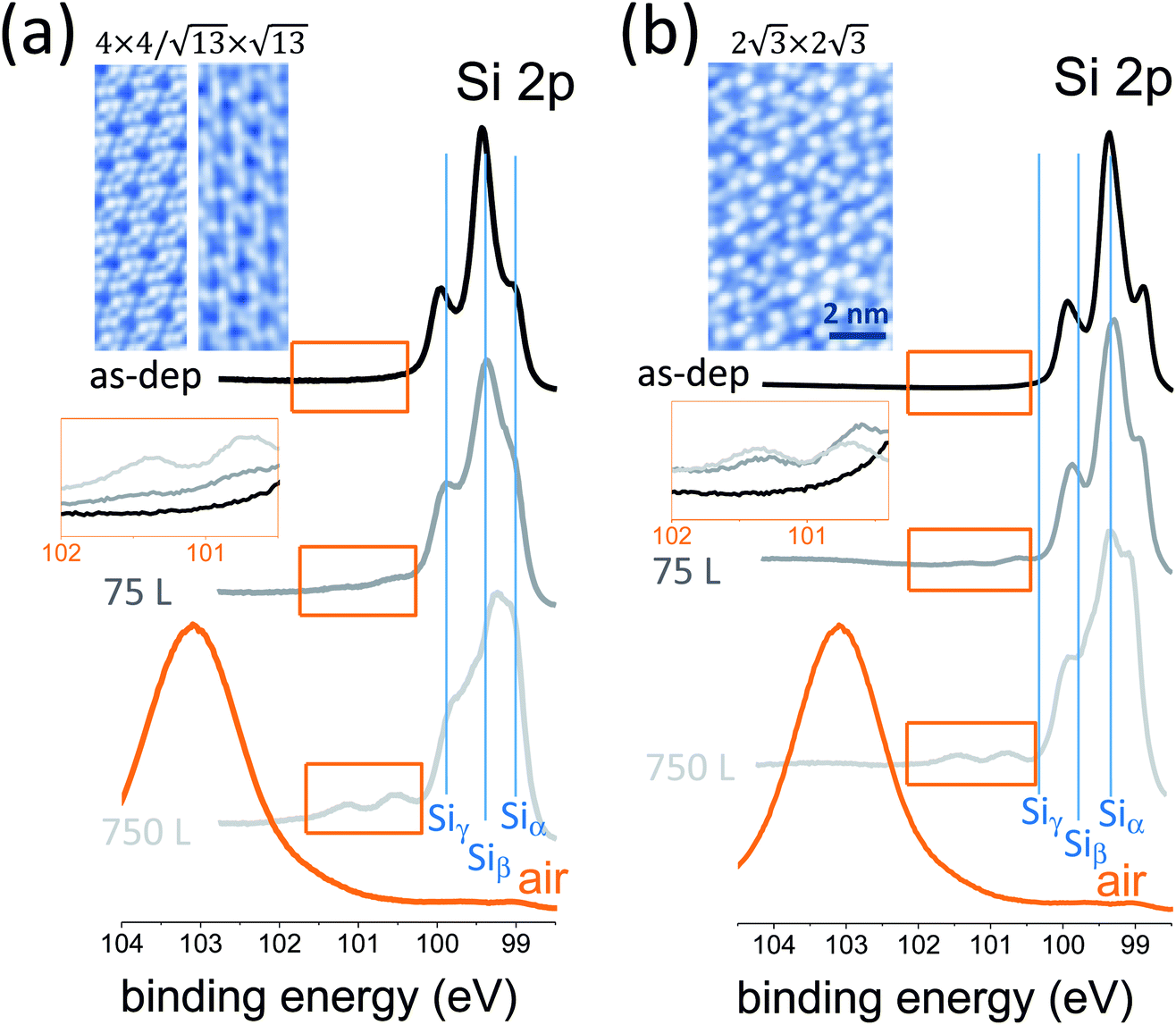 | ||
| Fig. 1 Si 2p core level photoemission lines (from top to bottom) for freshly grown silicene-on-silver, after 75 L O2 exposure, after 750 L O2 exposure, and after exposure to air. Core level lines are reported for two different silicene configurations, the 4 × 4/√13 × √13 mixed phase (a) and the 2√3 × 2√3 phase (b). Images at the top of each panel are scanning tunneling topographies of the two configurations. Insets in both panels (intermediate position on the left side of the panels) are magnifications of a limited range of the Si 2p lines in order to elucidate the O2-induced oxidation of silicene. | ||
Ultimately, if silicene is exposed to air, complete oxidation to a SiO2 compound takes place, as follows from the emergence of a broad peak at 103.50 eV corresponding to the Si4+ valence state in Si bonding. In this latter stage, it is not clear at the moment whether this silicene-derived SiO2 is recast as a 2D oxide layer (conformal to the original silicene) or as a clustered adsorbate. Open questions remain as to what kind of oxidation may take place when considering multilayer silicene as an alternative configuration to conventional cubic-structured silicon, which may unravel new mechanisms for silicon oxidation. More specifically, we wonder whether silicene can be uniformly oxidized so as to form a 2D silicon oxide either in a single layer or in a multilayer state. If so, we also wonder to what extent this silicene oxide would differ from the 2D silicon oxide frameworks grown on metal surfaces as reported by Büchner et al.14 This is an interesting set of questions aimed at the development of a new type of 2D insulator.
Encapsulation of silicene
The experimental framework
The environmental oxidation of silicene is a hurdle for its usage in applications. Methods to save silicene from degradation have been in demand since the early stages of silicene’s debut. One possible effective option turned out to be Al2O3 encapsulation sequentially carried out in UHV conditions after silicene growth by means of reactive co-deposition of an atomic Al beam with O2 molecules.15 This methodology results in the preservation of the chemical environment of silicene by means of a protective Al2O3 layer on silicene by sequentially growing elemental Al in the first stage, and Al in an O2-rich environment in the second stage. The initial elemental Al prevents silicon from oxidation when inletting O2 gas in the second stage, so as to have an overall Al2O3 layer at the end. No chemical interaction occurs between silicene and Al2O3, as demonstrated by the unaltered shape profile of the Si 2p core level photoemission line in Fig. 2a prior to and after Al2O3 deposition. An extra Ag 4s feature from the substrate does not appear in the Si 2p line of the pristine silicene after encapsulation, owing to the added Al2O3 thickness and consequent reduced substrate sensitivity in the photoemission. The Al2O3 encapsulation presents several benefits. It is a sequential process with silicene epitaxy within the same UHV environment. As such, it is not affected by collateral contamination. It works as an insulating layer for applications where a gate is needed. The effectiveness of the Al2O3 encapsulation is phenomenological evidence substantiated by in situ X-ray photoelectron spectroscopy (XPS) and ex situ Raman spectroscopy, as reported in Fig. 2.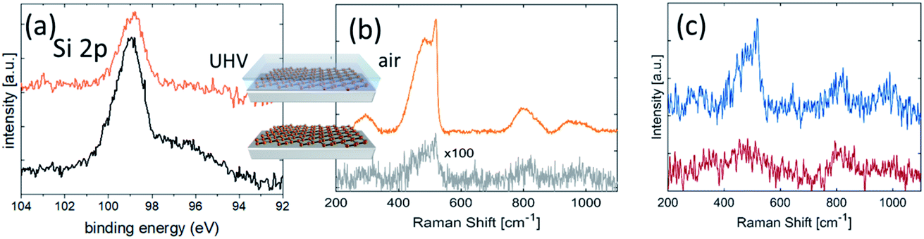 | ||
| Fig. 2 (a) Si 2p core-level photoemission lines taken on freshly grown silicene-on-silver (bottom) and after Al2O3 encapsulation (top). The right-side feature in the former spectrum is related to Ag 4s photoemission from the substrate, and is no longer detected in the encapsulated silicene owing to the Al2O3 layer thickness (∼5 nm); (b) Raman spectra of (top) capped and (bottom) uncapped silicene/Ag(111). In both cases the samples are exposed to air when recording the Raman spectrum and the silicene lattice is preserved only in the case of the encapsulated sample; (c) Raman spectra of unprotected silicene/Ag(111) obtained after 1 minute (top: same as the bottom spectrum in panel (b)) and ∼5 minutes after air exposure (bottom). The spectra are vertically stacked for clarity. | ||
As an identification probe, Raman spectroscopy has generally proved to be a superior tool to identify graphene and graphene-related materials.16 It was used for silicene too in order to check the silicene integrity after encapsulation, as reported in Fig. 2a. This is demonstrated in the comparative Raman spectroscopy study in Fig. 2b. In detail, Fig. 2b compares the encapsulated silicene (in air) with uncapped silicene in the early stage of degradation upon exposure to ambient air. The spectrum of silicene-on-silver(111) acquired just after its exposure to ambient conditions shows a feature around 500 cm−1, composed of a prominent narrow peak at 516 cm−1, plus a broad shoulder on the lower energy side (∼460 cm−1). These features are comparable with the Raman active modes of silicene-on-silver(111) substrates maintained in UHV conditions17 and, together with the band at 800 cm−1, are indicative of the presence of a partially oxidized ordered SiO2 phase.18 More detailed characterization of the Raman spectrum of silicene is extensively reported elsewhere.9 Here we emphasize the effectiveness of encapsulation in preserving silicene from degradation upon direct exposure. Nonetheless, fast degradation occurs for both silicene configurations after exposure to air if uncapped, as seen from the XPS spectra reported in Fig. 1. The dynamics of silicene oxidation are so fast that close real-time monitoring of silicene evolution is necessary to unveil the mechanism of Si reactivity under environmental conditions. As uncapped silicene is extracted from the growth chamber and brought into ambient lab conditions, the reaction with O2 occurs immediately, as evidenced by the Raman spectrum reported in Fig. 2c. Sizable modifications affect the Raman spectrum as a function of the exposure time. The disappearance of the sharp peak is accompanied by the broadening of the feature at 500 cm−1, whose intensity becomes comparable with the feature at 800 cm−1. These two observations may reflect the complete amorphization of the SiO2 phase resulting from early exposure, thus confirming the recent results obtained by means of in situ Raman spectroscopy at a low O2 dose.19 The dynamics of the bare silicene/Ag(111) exposed to ambient conditions are clearly dominated by the reaction with O2. The overall process could be depicted as a two-step reaction. The early interaction of the silicene layer with O2 leads to the formation of partially ordered SiO2 phase clusters with a small portion of silicene in its original structure. As the process progresses, the system evolves towards the amorphous phase of thin cluster-assembled SiOx. To confirm this two-step picture and describe the silicene degradation process, in situ monitoring of the structural properties of the system as a function of the O2 dose would help to disentangle the two proposed kinetics. The initial tendency of the silicene layer to preserve its order may be related to the interaction with the metallic substrate that makes the Si atoms less prone to oxidation.
Overall, a question arises regarding which mechanism favours Al2O3 accommodation on silicene-on-Ag without apparently affecting its structure.
A theoretical framework
An argument to support the picture as outlined above comes from preliminary density functional theory (DFT) simulations of silicene reactivity towards Al atom adsorption first, and Al2O3 accommodation second. We propose simulations for two different configurations, free-standing silicene and silicene-on-Ag. In order to further investigate this mechanism, a preliminary ab initio investigation of the interaction between Al or O2 and a 4 × 4 reconstruction of silicene on Ag(111) has been performed by means of DFT calculations detailed in the methods section. The results of the structural relaxations are summarized in Fig. 3, where two relevant aspects can be highlighted. First, an Al atom (light blue sphere) turns out to be favorably incorporated into the crystal lattice of free-standing silicene and it strongly affects the silicene structure (blue sphere lattice) after relaxation (Fig. 3a), whereas the same atom on Ag-supported silicene (Fig. 3b) tends to move apart from the Si surface upon relaxation. Hence, one can infer that the silicene layer is chemically “protected” by the hybridization of the Si atoms with the Ag atoms of the substrate, and in fact the calculated binding energy of the Al atom on the silicene layer is reduced by about 0.25 eV in the presence of the Ag substrate, as compared to the free-standing case. It should be noted that this is tendential behavior for an individual Al adatom accommodated on the silicene face that can hardly be matched with the collective behavior of an Al layer grown on silicene. Nonetheless, this individual picture gives us an idea of the tendential influence of the Ag substrate on silicene reactivity during Al2O3 deposition. In the latter case, the “lower reactivity” of the Ag-supported silicene (compared to the free-standing case) leads the O2 molecules (O atoms are depicted as red spheres in Fig. 3) to preferably bind with the Al atoms, resulting in a relaxed structure that only marginally influences the silicene bonds (see Fig. 3c, which illustrates the as-grown and relaxed Al2O3 on Ag-supported silicene). It should be noted that this picture is only specific to the Ag-supported silicene and may fail in other cases, e.g. silicene on ZrB2, where the extent of hybridization between the silicene layer and the substrate can change. Although it was noted that effective encapsulation can be substrate-dependent,20 this preliminary outcome suggests a method to apply Al2O3 encapsulation to Xenes supported by noble metal surfaces.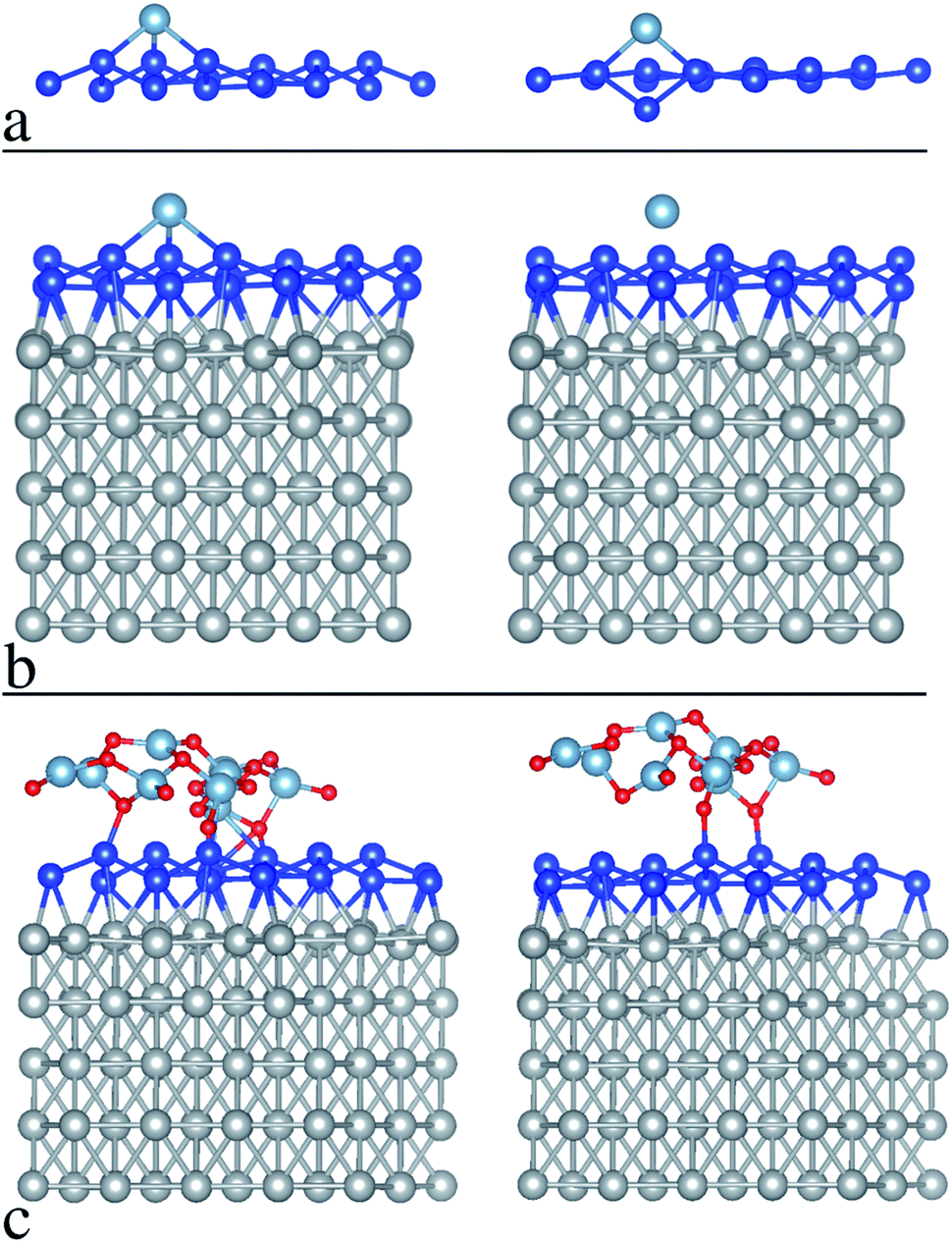 | ||
| Fig. 3 DFT simulation before relaxation (left) and after relaxation (right) in the case of: (a) Al atom absorption to free-standing silicene, (b) Al atom absorption to silicene-on-silver, (c) Al2O3 accommodation on silicene-on-silver. | ||
Though preliminary, these data show that the Al2O3 capping protocol can be applied to epitaxial Xenes with an interaction with the substrate strong enough to inhibit or minimize chemisorption to Al adatoms. This usually happens on noble metal surfaces hosting an Xene layer, as in the case of silicene-on-silver, and should be further investigated for silicene deposition on sapphire.21 A question arises as to whether other Xenes of the same kind may benefit from such an encapsulation scheme. More generally, we wonder whether the encapsulation reported here can be taken as a universal methodology for Xenes on metal surfaces. In the following section we partially address this by taking into account the case of epitaxial phosphorene.
Encapsulation of epitaxial phosphorene
The strategy developed for the encapsulation of silicene on a metallic substrate has been fruitfully exploited to prevent the oxidation of exfoliated black phosphorous flakes on SiO2/Si substrate.22 The encapsulation thus also works for highly reactive van der Waals materials on inert substrates. Therefore, it is interesting to further explore its applicability to the vast family of 2D materials with a focus on epitaxial Xenes.Epitaxial phosphorene is a good case for which to validate Al2O3 encapsulation for metal-supported Xenes beyond silicene-on-silver. Epitaxial phosphorene results from the vacuum evaporation of a P4 molecular flux that undergoes dissociative chemisorption when ground on an Au(111) surface. In the substrate temperature range 240–270 °C, chemisorbed phosphorus molecular species self-arrange in a flower-like honeycomb pattern with hexagonal symmetry, as shown in the atomically resolved scanning tunneling microscopy (STM) topography in Fig. 4a. We name this structure epitaxial phosphorene to discriminate it from a single layer of black phosphorus, conventionally termed phosphorene. In contrast to silicene, epitaxial phosphorene possesses a local semiconducting character23,24 and completely covers the Au terraces with a single superstructure (Fig. 4b). The observed morphology was originally attributed to an epilayer with the same buckled structure of the theoretically predicted free-standing blue-phosphorene lattice. In this model all the petals of the flower-like pattern correspond to P16 blue-phosphorene islands matching half of the 5 × 5 Au(111) unit cell.23–25 However, close inspection of the high-resolution STM image in Fig. 4a reveals that only a few petals show six bright protrusions typical of a P16 blue-phosphorene island, while most of them consist of three bright protrusions. This has been explained by introducing a model where two local atomic configurations may coexist together.26,27 Beside sparse P16 blue-phosphorene islands (see the blue rhombus in Fig. 4a), “adatom-rich” structures are also possible. In the “adatom-rich” structure three additional phosphorus atoms are accommodated on the top layer (see the yellow rhombus in Fig. 4a). More recently, a new interpretation of the structure of epitaxial phosphorene questioned all the previously discussed atomic models. As reported in ref. 28, the structure of epitaxial phosphorene may correspond to an Au-decorated phosphorene network rather than an epilayer. According to this model, the triangular petals coincide with buckled blue-phosphorene P9 monomers (with the top three P atoms protruding at a larger distance from the Au substrate) linked to three other P9 monomers on their sides by gold adatoms coming from the substrate (see the green rhombus in Fig. 4a).
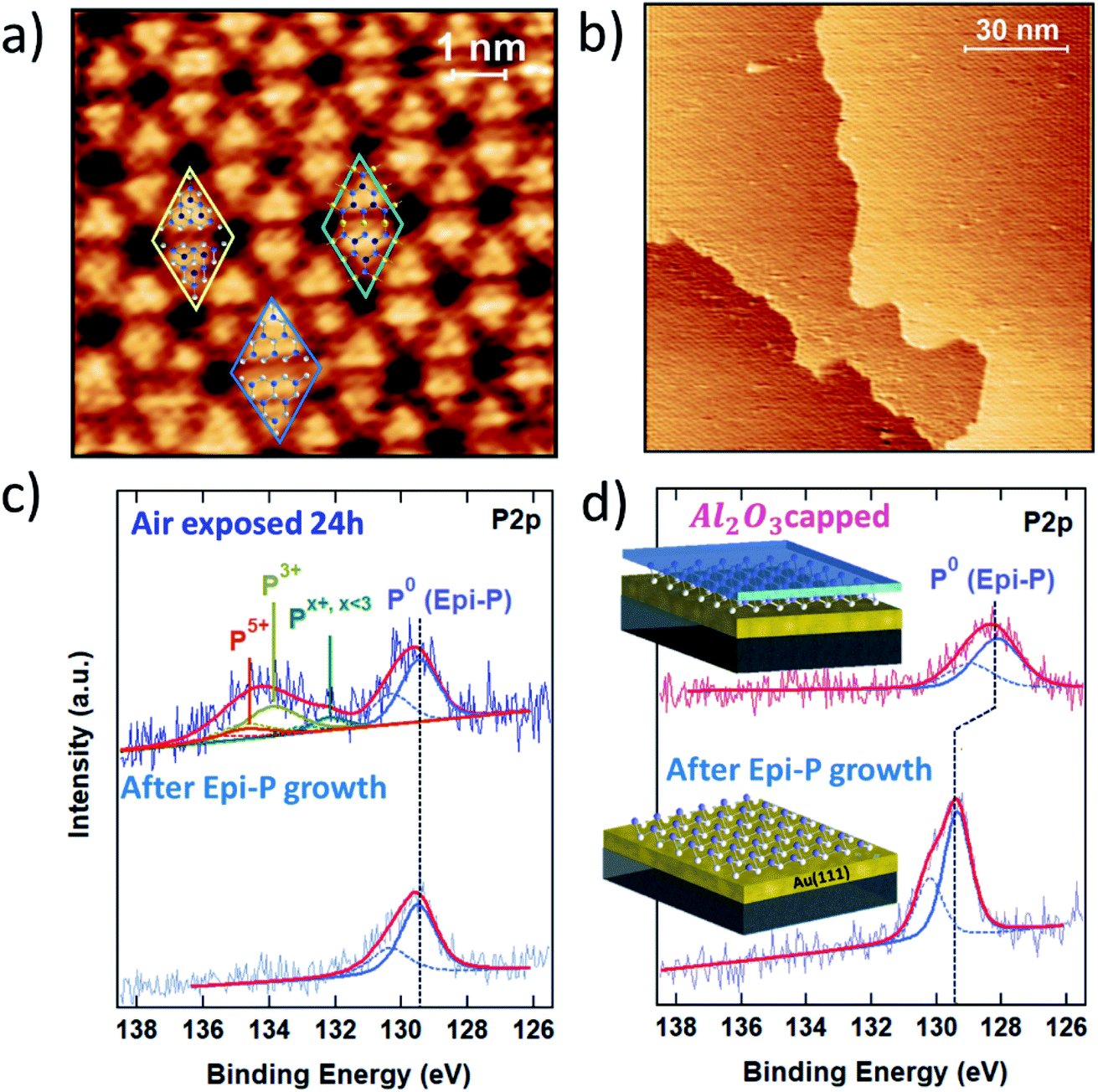 | ||
| Fig. 4 (a) High-resolution 8 × 8 nm2 STM image of epitaxial phosphorene. The rhombi are (5 × 5) unit cells enclosing local atomic models proposed for epitaxial phosphorene: the P16 blue-phosphorene structure (blue), the “adatom-rich” structure (yellow) and the recently proposed Au-decorated phosphorene network (green). In the overlapping models P atoms are represented by white, light blue and dark blue spheres according to the distance from the substrate, and Au atoms by yellow spheres. (b) Large-scale 130 nm × 130 nm2 STM image of epitaxial phosphorene; (c) comparative XPS study of the P 2p line of freshly grown epitaxial phosphorene (bottom) and after exposure to air (top); (d) comparative XPS study of the P 2p line of freshly grown epitaxial phosphorene (bottom) and after Al2O3 encapsulation (top). | ||
Like silicene (but to a different extent), epitaxial phoshorene is subject to oxidation when exposed to air. Its stability is elucidated in the comparative XPS study in Fig. 4c, where the P 2p core level photoemission line is reported for freshly grown epitaxial phosphorene (bottom) and after exposure to air (top). As can be noted from the permanence of the elementary P–P bonding component (denoted P0 in Fig. 4c), at 129.4 eV epitaxial phosphorene still survives after air exposure, in marked contrast to silicene. The photoemitted P 2p core electrons of air-exposed epitaxial phosphorene show a broad oxide peak from 132 to 136 eV. By fitting this oxide peak through spin–orbit doublets with a separation of 0.86 eV and a fixed 2![[thin space (1/6-em)]](https://www.rsc.org/images/entities/char_2009.gif) :1 intensity ratio, the resulting components at 134.7 eV and 133.8 eV can be attributed to phosphorus oxidation states of +5 and +3, respectively, whereas the component at 132.1 eV can be assigned to lower oxidation states. Thus, the oxidation of epitaxial phosphorene in air may involve the formation of P2O5 and P2O3 oxides and P2Ox,x<3 suboxides, similar to what has been reported for air-exposed black phosphorus films.29,30 Oxygen is known to play an important role in the preliminary stages of black phosphorus oxidation,31 but alone does not lead to a complete physical degradation of the material. Short-term exposure to high-purity O2 has been shown to oxidize few-layer black phosphorus at a much slower rate than the combined action of oxygen and water producing low oxidation states.31 Similarly, epitaxial phosphorene shows a remarkably high oxidation endurance to limited molecular oxygen dosing in UHV.26 At higher doses, oxygen atoms preferentially absorb on top of one of the protruding phosphorus trimers without degrading the epitaxial phosphorene superstructure.32 These facts reveal a peculiar oxidation chemistry of epitaxial phosphorene that differs from that of silicene and shares some similarities with the oxidation mechanism of black phosphorus. Accurate investigations are needed to disentangle the oxidation scheme of epitaxial phosphorene and resolve open questions such as the chemistry of epitaxial phosphorene with water, alone or in combination with another oxidizing agent like oxygen, as well as the influence of exposure to light.
:1 intensity ratio, the resulting components at 134.7 eV and 133.8 eV can be attributed to phosphorus oxidation states of +5 and +3, respectively, whereas the component at 132.1 eV can be assigned to lower oxidation states. Thus, the oxidation of epitaxial phosphorene in air may involve the formation of P2O5 and P2O3 oxides and P2Ox,x<3 suboxides, similar to what has been reported for air-exposed black phosphorus films.29,30 Oxygen is known to play an important role in the preliminary stages of black phosphorus oxidation,31 but alone does not lead to a complete physical degradation of the material. Short-term exposure to high-purity O2 has been shown to oxidize few-layer black phosphorus at a much slower rate than the combined action of oxygen and water producing low oxidation states.31 Similarly, epitaxial phosphorene shows a remarkably high oxidation endurance to limited molecular oxygen dosing in UHV.26 At higher doses, oxygen atoms preferentially absorb on top of one of the protruding phosphorus trimers without degrading the epitaxial phosphorene superstructure.32 These facts reveal a peculiar oxidation chemistry of epitaxial phosphorene that differs from that of silicene and shares some similarities with the oxidation mechanism of black phosphorus. Accurate investigations are needed to disentangle the oxidation scheme of epitaxial phosphorene and resolve open questions such as the chemistry of epitaxial phosphorene with water, alone or in combination with another oxidizing agent like oxygen, as well as the influence of exposure to light.
The effect of the Al2O3 encapsulation of epitaxial phosphorene is elucidated in Fig. 4d by comparing the P 2p line prior to and after Al2O3 capping. Despite the reduced photoemission intensity (due to the extra thickness of the Al2O3 top layer), the shape profile of the P 2p line shows no substantial change except for a −1.2 eV shift of the binding energy between the two lines (to a lesser extent a similar shift is also observed for silicene on Ag). The former fact validates the encapsulating action of the Al2O3 layer and positions Al2O3 encapsulation as a candidate for a general approach to the stabilization of Xenes supported on metal substrates. The latter fact stems from the peak positioning with reference to the Au 4f peaks (binding energy positioning of the core level peaks is calibrated using the Au 4f position as usual, for each process stage). Shifts in the binding energies can be due to charge incorporation causing the Fermi level to move away from its pristine position in the uncapped layer. We interpret this behaviour as being due to an interface dipole formation around the phosphorene environment, according to which fixed charges intrinsic to the Al2O3 film are compensated by an image charge in the Au/phosphorene superstructure.33,34 This picture is corroborated by the observation that the original binding energy is restored whenever the Al2O3 capped phosphorene is exposed to air (data not shown), as far as the environmental reactivity may induce the saturation of charged defects in Al2O3 and a reset of the electrical balance between the stacks.
Oxidation of epitaxial phosphorene is a key aspect to understand in order to develop processing protocols such as layer transfer aiming at device fabrication. Recently, it was shown that Al2O3 encapsulation can save epitaxial phosphorene from complete degradation in a wet environment (used for substrate etching).26 Nonetheless, partial oxidation takes place and it is not clear at the moment what the relevant reactivity path is. This will open a framework to engineer processes enabling the full exploitation of large-scale phosphorus at the 2D level, thus bypassing the current size limitation of black phosphorus flakes.
Summary
Xenes are a new frontier in the physics and chemistry of 2D materials. However, their stability in environmental conditions is a hurdle for applications. This Discussion provides a playground to explore several aspects of the chemical reactivity of Xenes and to develop a general methodology to prevent the environmental degradation of Xenes out of vacuum. The general character of the Discussion is to propose data inspiring open questions or issues yet to be solved. In detail, the first aspect considered is the chemical reactivity upon O2 exposure and in air. This is showcased in the paradigmatic epitaxial silicene-on-silver by means of photoemission and Raman spectroscopy investigations. Second, a solution to the fast degradation of silicene is proposed, which consists of the sequential encapsulation of silicene with an Al2O3 capping layer. The effectiveness of the approach is substantiated and supported by a preliminary DFT model suggesting that the silicene–silver interaction is a key mechanism to save silicene integrity after Al2O3 deposition. This idea is further developed for epitaxial phosphorene-on-gold in order to validate the universality of the approach for the Xene-on-metal framework. In the latter case, the encapsulation works as effective protection and, due to the peculiar charge exchange at the Al2O3–phosphorene interface, dipole-induced electronic band bending is reported as an effect of the heterostructure. Additional Xenes on metal substrates will represent promising tests to unravel possible universal oxidation mechanisms as well as to develop encapsulation processes.Methods
Sample growth
Epitaxial growth of Xenes was performed in UHV conditions (base pressure 10−10 mbar) in a temperature range of 210–290 °C by means of molecular flux released from e-beam evaporators or effusion cells on metal (Ag, Au) film surfaces supported by mica substrates and prepared by several cycles of Ar+ (1 keV) sputtering and annealing at 500 °C. Oxygen dosage experiments were performed in the UHV environment by exposing the silicene surface to an O2-rich atmosphere (100 s and 1000 s at 1 × 10⁻⁶ mbar to get 75 and 750 L, respectively).Experimental characterization
Synchrotron radiation core-level photoemission spectroscopy in Fig. 1 was performed at the VUV-beamline at the Elettra Synchrotron Radiation facility in Italy, with the electron spectrometers placed at 45° with respect to the direction of the horizontally polarized photon beam and with a photon energy hν = 130 eV; XPS data in Fig. 2 and 4 were acquired by means of a non-monochromatic Mg Kα source (1253.6 eV) and their energy positioning was calibrated by taking the tabulated Ag and Au core-level positions as references for the case of silicene and phosphorene, respectively; Raman spectroscopy in Fig. 2 was performed with a single 60 s long acquisition by exploiting an Invia Renishaw spectrometer equipped with the 514.5 nm wavelength of an Ar+ laser Raman spectrum; STM topographies in Fig. 1 and 4 were acquired at room temperature with an Omicron scanning tunneling microscope (STM) equipped with a homemade chemically etched tungsten tip.DFT modelling details
Ab initio simulations are performed by exploiting DFT with PBE exchange-correlation potential in a generalized gradient approximation (GGA)35 and using a non-local functional for the van der Waals forces,36 as implemented in Quantum Espresso.37 We use a plane-wave basis set with a kinetic energy cutoff of 40 Ry and the Γ point for sampling the Brillouin zone of the simulated supercell. The silicene/Ag system has been modeled by a supercell containing 5 Ag(111) atomic layer with the silicene layer on top. The supercell is periodic in the x–y directions, while 15 Å of vacuum has been exploited to avoid interactions between periodic replica in the z direction and a dipole correction has been also used. A single Al atom, an O2 molecule, or an Al2O12 cluster has been inserted on the silicene surface at an initial distance that ensures the formation of bonds between the Si atoms of the silicene layer and the Al or O atoms on top. Then structural relaxations have been performed until the average atomic force was lower than 10−4 Ry per Bohr, by using a quasi-Newton algorithm, both including the Ag substrate and considering a bare free-standing silicene layer.Conflicts of interest
There are no conflicts to declare.Acknowledgements
The authors acknowledge P. Moras, S. Sanjoy, and C. Carbone (CNR-ISM, Trieste, Italy) for support with the synchrotron measurements. A. M., C. M. and C. G. acknowledge financial support from H2020 Framework Programme funding, call ERC CoG 2017 Grant N. 772261 “XFab”.Notes and references
- C. Grazianetti, C. Martella and A. Molle, Phys. Status Solidi RRL, 2019, 1900439 Search PubMed.
- A. Molle, J. Goldberger, M. Houssa, Y. Xu, S. C. Zhang and D. Akinwande, Nat. Mater., 2017, 16, 163–169 CrossRef CAS.
- Y. Xu, B. Yan, H.-J. Zhang, J. Wang, G. Xu, P. Tang, W. Duan and S.-C. Zhang, Phys. Rev. Lett., 2013, 111, 136804 CrossRef.
- A. J. Mannix, B. Kiraly, M. C. Hersam and N. P. Guisinger, Nat. Rev. Chem., 2017, 1, 0014 CrossRef CAS.
- Y. Yamada-Takamura and R. Friedlein, Sci. Technol. Adv. Mater., 2014, 15, 064404 CrossRef.
- A. Molle, C. Grazianetti, L. Tao, D. Taneja, M. H. Alam and D. Akinwande, Chem. Soc. Rev., 2018, 47, 6370–6387 RSC.
- L. Tao, E. Cinquanta, D. Chiappe, C. Grazianetti, M. Fanciulli, M. Dubey, A. Molle and D. Akinwande, Nat. Nanotechnol., 2015, 10, 227–231 CrossRef CAS.
- C. Grazianetti, D. Chiappe, E. Cinquanta, G. Tallarida and M. Fanciulli, Appl. Surf. Sci., 2014, 291, 109–112 CrossRef CAS.
- E. Cinquanta, E. Scalise, D. Chiappe, C. Grazianetti, B. Van Den Broek, M. Houssa, M. Fanciulli and A. Molle, J. Phys. Chem. C, 2013, 117, 16719 CrossRef CAS.
- J. Avila, P. De Padova, S. Cho, I. Colambo, S. Lorcy, C. Quaresima, P. Vogt, a. Resta, G. Le Lay and M. C. Asensio, J. Phys.: Condens. Matter, 2013, 25, 262001 CrossRef CAS.
- A. Fleurence, R. Friedlein, T. Ozaki, H. Kawai, Y. Wang and Y. Yamada-Takamura, Phys. Rev. Lett., 2012, 108, 245501 CrossRef.
- D. Chiappe, C. Grazianetti, G. Tallarida, M. Fanciulli and A. Molle, Adv. Mater., 2012, 24, 5088–5093 CrossRef CAS.
- Y. Du, J. Zhuang, J. Wang, Z. Li, H. Liu, J. Zhao, X. Xu, H. Feng, L. Chen, K. Wu, X. Wang and S. X. Dou, Sci. Adv., 2016, 2, e1600067 CrossRef.
- C. Büchner, Z.-J. Wang, K. M. Burson, M.-G. Willinger, M. Heyde, R. Schlögl and H.-J. Freund, ACS Nano, 2016, 10, 7982–7989 CrossRef.
- A. Molle, C. Grazianetti, D. Chiappe, E. Cinquanta, E. Cianci, G. Tallarida and M. Fanciulli, Adv. Funct. Mater., 2013, 23, 4340–4344 CrossRef CAS.
- A. C. Ferrari and D. M. Basko, Nat. Nanotechnol., 2013, 8, 235–246 CrossRef CAS.
- D. Solonenko, O. D. Gordan, G. Le Lay, H. Şahin, S. Cahangirov, D. R. T. Zahn and P. Vogt, 2D Mater., 2016, 4, 015008 CrossRef.
- F. L. Galeener, A. J. Leadbetter and M. W. Stringfellow, Phys. Rev. B, 1983, 27, 1052–1078 CrossRef CAS.
- D. Solonenko, O. Selyshchev, D. R. T. Zahn and P. Vogt, Phys. Status Solidi, 2019, 256, 1800432 CrossRef.
- R. Friedlein, H. Van Bui, F. B. Wiggers, Y. Yamada-Takamura, A. Y. Kovalgin and M. P. de Jong, J. Chem. Phys., 2014, 140, 204705 CrossRef CAS.
- C. Grazianetti, S. De Rosa, C. Martella, P. Targa, D. Codegoni, P. Gori, O. Pulci, A. Molle and S. Lupi, Nano Lett., 2018, 18, 7124–7132 CrossRef CAS.
- J. D. Wood, S. A. Wells, D. Jariwala, K.-S. Chen, E. Cho, V. K. Sangwan, X. Liu, L. J. Lauhon, T. J. Marks and M. C. Hersam, Nano Lett., 2014, 14, 6964–6970 CrossRef CAS.
- J. L. Zhang, S. Zhao, C. Han, Z. Wang, S. Zhong, S. Sun, R. Guo, X. Zhou, C. D. Gu, K. Di Yuan, Z. Li and W. Chen, Nano Lett., 2016, 16, 4903–4908 CrossRef CAS.
- J. Zhuang, C. Liu, Q. Gao, Y. Liu, H. Feng, X. Xu, J. Wang, J. Zhao, S. X. Dou, Z. Hu and Y. Du, ACS Nano, 2018, 12, 5059–5065 CrossRef CAS.
- E. Golias, M. Krivenkov, A. Varykhalov, J. Sánchez-Barriga and O. Rader, Nano Lett., 2018, 18, 6672–6678 CrossRef CAS.
- C. Grazianetti, G. Faraone, C. Martella, E. Bonera and A. Molle, Nanoscale, 2019, 11, 18232–18237 RSC.
- W. Zhang, H. Enriquez, Y. Tong, A. Bendounan, A. Kara, A. P. Seitsonen, A. J. Mayne, G. Dujardin and H. Oughaddou, Small, 2018, 14, 1804066 CrossRef.
- H. Tian, J.-Q. Zhang, W. Ho, J.-P. Xu, B. Xia, Y. Xia, J. Fan, H. Xu, M. Xie and S. Y. Tong, Matter, 2020, 2, 111–118 CrossRef.
- K. L. Kuntz, R. A. Wells, J. Hu, T. Yang, B. Dong, H. Guo, A. H. Woomer, D. L. Druffel, A. Alabanza, D. Tománek and S. C. Warren, ACS Appl. Mater. Interfaces, 2017, 9, 9126–9135 CrossRef CAS.
- W. Luo, D. Y. Zemlyanov, C. A. Milligan, Y. Du, L. Yang, Y. Wu and P. D. Ye, Nanotechnology, 2016, 27, 434002 CrossRef.
- A. Ziletti, A. Carvalho, D. K. Campbell, D. F. Coker and A. H. Castro Neto, Phys. Rev. Lett., 2015, 114, 046801 CrossRef CAS.
- J. L. Zhang, S. Zhao, M. Telychko, S. Sun, X. Lian, J. Su, A. Tadich, D. Qi, J. Zhuang, Y. Zheng, Z. Ma, C. Gu, Z. Hu, Y. Du, J. Lu, Z. Li and W. Chen, Nano Lett., 2019, 19, 5340–5346 CrossRef CAS.
- L. Kornblum, J. A. Rothschild, Y. Kauffmann, R. Brener and M. Eizenberg, Phys. Rev. B: Condens. Matter Mater. Phys., 2011, 84, 155317 CrossRef.
- Y. Wu, H.-S. Tao, E. Garfunkel, T. E. Madey and N. D. Shinn, Surf. Sci., 1995, 336, 123–139 CrossRef CAS.
- J. P. Perdew, K. Burke and M. Ernzerhof, Phys. Rev. Lett., 1996, 77, 3865–3868 CrossRef CAS.
- M. Dion, H. Rydberg, E. Schröder, D. C. Langreth and B. I. Lundqvist, Phys. Rev. Lett., 2004, 92, 246401 CrossRef CAS.
- P. Giannozzi, S. Baroni, N. Bonini, M. Calandra, R. Car, C. Cavazzoni, D. Ceresoli, G. L. Chiarotti, M. Cococcioni, I. Dabo, A. Dal Corso, S. de Gironcoli, S. Fabris, G. Fratesi, R. Gebauer, U. Gerstmann, C. Gougoussis, A. Kokalj, M. Lazzeri, L. Martin-Samos, N. Marzari, F. Mauri, R. Mazzarello, S. Paolini, A. Pasquarello, L. Paulatto, C. Sbraccia, S. Scandolo, G. Sclauzero, A. P. Seitsonen, A. Smogunov, P. Umari and R. M. Wentzcovitch, J. Phys.: Condens. Matter, 2009, 21, 395502 CrossRef.
Footnote |
| † Present address: ASM Microchemistry, Pietari Kalmin katu 3, 00560 Helsinki (FI). |
| This journal is © The Royal Society of Chemistry 2021 |