
 Open Access Article
 This Open Access Article is licensed under a
 Creative Commons Attribution 3.0 Unported Licence
Design considerations for multi-terawatt scale manufacturing of existing and future photovoltaic technologies: challenges and opportunities related to silver, indium and bismuth consumption
Yuchao
Zhang†
 *a,
Moonyong
Kim†
a,
Li
Wang
a,
Pierre
Verlinden
abcd and
Brett
Hallam
a
*a,
Moonyong
Kim†
a,
Li
Wang
a,
Pierre
Verlinden
abcd and
Brett
Hallam
a
aSchool of Photovoltaic and Renewable Energy Engineering, University of New South Wales, Sydney, Australia. E-mail: Yuchao.Zhang@unsw.edu.au
bAMROCK Australia Pty Ltd., PO Box 714, McLaren Vale, SA 5171, Australia
cInstitute for Solar Energy Systems, Sun Yat-Sen University, Guangzhou, China
dState Key Laboratory of PVST, Trina Solar, Changzhou, China
First published on 27th September 2021
Abstract
To significantly impact climate change, the annual photovoltaic (PV) module production rate must dramatically increase from ∼135 gigawatts (GW) in 2020 to ∼3 terawatts (TW) around 2030. A key knowledge gap is the sustainable manufacturing capacity of existing and future commercial PV cell technologies imposed by scarce metals, and a suitable pathway towards sustainable manufacturing at the multi-TW scale. Assuming an upper material consumption limit as 20% of 2019 global supply, we show that the present industrial implementations of passivated emitter and rear cell (PERC), tunnel oxide passivated contact (TOPCon), and silicon heterojunction (SHJ) cells have sustainable manufacturing capacities of 377 GW (silver-limited), 227 GW (silver-limited) GW and 37 GW (indium-limited), respectively. We propose material consumption targets of 2 mg W−1, 0.38 mg W−1, and 1.8 mg W−1 for silver, indium, and bismuth, respectively, indicating significant material consumption reductions are required to meet the target production rate for sustainable multi-TW scale manufacturing in about ten years from now. The industry needs urgent innovation on screen printing technologies for PERC, TOPCon, and SHJ solar cells to reduce silver consumption beyond expectation in the Industrial Technology Roadmap for PV (ITPRV), or the widespread adoption of existing and proven copper plating technologies. Indium cannot be used in any significant manufacturing capacity for PV production, even for futuristic 30%-efficient tandem devices. The current implementation of low-temperature interconnection schemes using bismuth-based solders will be limited to 330 GW of production. With half the silver-limited sustainable manufacturing capacity as PERC, the limited efficiency gains of SHJ and TOPCon cell technologies do not justify a transition away from industrial PERC, or the introduction of indium- and bismuth limitations for SHJ solar cells. On the other hand, futuristic two-terminal tandems with efficiency potentials over 30% have a unique opportunity to reduce material consumption through substantially reduced series resistance losses.
Broader contextTo meet the Paris Agreement target limiting global warming to 2 °C, photovoltaics, the conversion of sunlight into electricity, is expected to play a key role in the transition from using traditional fossil fuels to renewable energy. During the past decade, the photovoltaics industry has demonstrated exponential growth, technological advancements, and significant cost reductions to become the cheapest form of new electricity. As the photovoltaics industry heads towards a potential 30-fold increase to multi-terawatt scales of annual production over the coming decade on its path to become the dominant energy source, a critical concern is material consumption for scarce metals including silver, indium and bismuth. This work provides a comprehensive understanding of the interdependencies between physical dimensions of metallic structures, material consumption and device performance for existing and future solar cell technologies, highlighting key requirements for sustainable terawatt scale manufacturing, critical challenges in reducing material consumption and opportunities for innovation. We identify the need for innovation in screen-printing and unique opportunities for tandems in the effort to reduce silver consumption. We also highlight the need to avoid introducing new material challenges such as indium and bismuth with the widespread deployment of ‘next-generation’ technologies, using approaches that are already proven. |
Introduction
Approximately 25% of global greenhouse gas emissions (GHG) come from electricity and heat generation, with one of the main sources of CO2 emissions being the burning of fossil fuels.1 One critical approach of reducing GHG is using cleaner and renewable energy sources such as solar energy, wind energy, geothermal energy, hydro energy, and biomass. To reduce the potential impact of fossil fuel usage on climate change, many countries have set targets of renewable energy penetration, for instance, 100% in Denmark, Switzerland, and United Kingdom by 2050,2 50% in Australia by 2030,3 40% in India by 2030,4 and 60% in China by 2050.5 Notably, remarkable progress in the transition to renewable energy has been made by some countries already. For example, countries like Norway and Iceland already achieved 100% of their electricity supply being produced from renewable energy only, such as hydro, geothermal and solar energy,2 and 18 other countries have reached a level of 80%.Every second, the amount of energy reaching the earth's surface from the Sun is enough to power humankind's energy requirements for approximately 2.7 hours.6 Photovoltaic (PV) technologies have pronounced advantages in accessing abundances of solar energy, predictable energy output based on the weather forecast, low land consumption, easy installation and maintenance, and low costs. Therefore, assuming a significant electrification of all energy sectors, using PV modules, with the direct conversion of sunlight into electricity, has great potential to play a central role in the future clean energy system. Although there is an emission during the manufacturing phase, due to little or no emission during the operation phase, PV can greatly reduce the greenhouse emissions to generate electricity in the long term.
Historically, PV was born as an expensive technology to satisfy the need for energy in remote locations such as high efficiency devices for space applications. For terrestrial applications, the first commercially sold solar cell at US$25 per cell with an efficiency of only around 10%.7 Since then, a tremendous amount of effort has been put into developing new cell technologies and increasing cell efficiencies. To date, the average efficiency of the mainstream industrial passivated emitter and rear cell (PERC) technology has already reached 22.5–23%,8–10 and an efficiency record for single-junction silicon solar cell at 26.7% was achieved by Kaneka et al. with an n-type silicon heterojunction (SHJ) solar cell with interdigitated back contacts.11 Integrating another solar cell on crystalline silicon solar cell to form a tandem structure, a record efficiency of 29.52% was demonstrated by Oxford PV.12
Meanwhile, technological advancements and exponential growth in the industrial size have been dramatically reducing the manufacturing cost of solar modules by more than two orders of magnitude comparing to that in 1980. Especially after 2008, the average selling price of commercial solar modules was reduced from US$4.12 W−1 in 2008 to US$0.17 W−1 in 2020, corresponding to a 24 times reduction within 12 years.13 A recent analysis by LAZARD estimates the levelized cost of energy (LCOE) of coal-fired power and PV in utility-scale at US$65–159 MW−1 h−1 and US$31–42 MW−1 h−1,14 respectively, demonstrating the great potential of PV as a cheap and sustainable replacement of the traditional fossil-fuel-based energy generation system.
In 2020, a total of 135 GW of PV module was produced, which subsequently brings the cumulative installed capacity of PV to more than 756 GW,10 accounting for about 4% in global electricity generation.15 However, to significantly reduce the carbon emissions from the power generation sector and to achieve the target of limiting global warming to well below 2 °C compared to pre-industrial levels set by the COP-21 Paris Agreement,16 several studies have suggested that a significant increase in the size of the PV industry is required, specifically, with a cumulative installed capacity of around 70 TW by 2050, and therefore, an annual production capacity of 3–4 TW by this time.17–19 Historically, the PV industry has already exhibited the capability of fast growth in the annual production capacity with an average two-fold increase in every three years.10 However, the continued aggressive growth of the PV industry and transition towards a major component in the global energy production system leads to a new concern on the availability of scarce elements being used for the manufacture of industrial solar cells and deployment of photovoltaic modules in the field.
At a systems level, copper is required for cables and transformer windings in balance of system (BoS) components and ribbons in cell interconnection in modules. The values of copper consumption at 2800 kg MW−1 in PV systems20 are approximately twice more than nuclear, coal, or natural gas power plants. However, the value of copper consumption in solar is similar to that of on-shore wind and lower than that of off-shore wind, and of no significant concern for terawatt-scale manufacturing with an annual copper supply of more than 24.6 megatonnes,21 particularly considering ongoing efficiency enhancements of solar panels. Aluminium is primarily used at the module level for aluminium framing with consumption of ∼9000 kg MW−1 for typical 17% efficient modules.22 With an even larger global aluminium supply scale of 130 megatonnes,23 aluminium consumption in the PV industry also does not impose any significant material challenges. As another commonly used material in BoS components such as racking systems and transformers, steel has a high consumption level of around 30–45 tonnes per MW.24 However, given the annual supply of 1800 megatonnes25 and average growth rate of 3–6% per year, the availability of steel also does not impose constraints to the PV manufacturing at the TW scale.
The primary concern for photovoltaics is silver due to its scarcity and widespread use in essentially all current implementations of industrial silicon solar cell technologies such as PERC, TOPCon, and SHJ. In addition, there are significant concerns for the use of indium if the manufacturing capacity of SHJ solar cells increases or for future tandem devices, and also the use of bismuth in the low-temperature interconnection approach typical for SHJ solar cells.
In this work, we consider the impact of solar cell efficiencies and physical geometries of metallic structures on the material consumption of silver, indium, and bismuth to assess the suitability of solar cell technologies for sustainable PV manufacturing at the terawatt scale. We then use the findings to highlight requirements for existing industrial solar cell technologies (PERC, TOPCon, and SHJ) and future implications for two-terminal (2T) tandem devices on Si-based bottom cells.
Global supply of silver, indium, and bismuth and industrial applications
The mass fraction of silver, indium, and bismuth in the earth's crust is estimated at 7.5 × 10⁻⁸, 2.5 × 10⁻⁷, and 8.5 × 10⁻⁹ kg kg−1, respectively.26 These values correspond to total material resources of approximately 2.1 × 10¹² tonnes, 6.9 × 10¹² tonnes, and 2.4 × 10¹¹ tonnes, respectively. However, realistically, only a certain fraction of these material resources can be considered as usable reserve for the PV industry. This is since the proven reserve is based on the availability, accessibility, and feasibility to extract the material both economically and technically.The recorded global silver (Ag) mineral reserve in 2019 was estimated at 560 kilotonnes.27 During the past decade, the global supply level of silver remains relatively stable, ranging between 2.8–3.0 × 10⁴ tonnes per year. Due to its high intrinsic values and excellent electroconductive quality, silver has a wide range of applications in modern society, such as in silverware, jewellery, coins and medals, photography, and in industrial processes and in electronics such as forming high-quality contacts on solar cells. On the demand side, ‘smarter’ devices with more functions require a circuit design with increased complexity and, therefore, a higher silver consumption. For instance, a modern smartphone produced in 2012 has 1500–2700 mg of silver embedded per kg of circuit boards, compared to only 100–500 mg in a cellular phone in 2004.28 In addition, all electric vehicles (EVs) and hybrid-electric vehicles (HEVs), as promising substitutes to conventional vehicles, consume 1–1.5 times more silver due to the high level of electrification.29 Consequently, the large-scale deployment of EVs and HEVs, as a key component of fighting climate change, is expected to drive the total silver demand of the automotive sector from 1600 tonnes in 2019 (5% of global supply) to around 4500 tonnes by 2040 (15% of global supply), where almost half of the silver demand in the auto sector will be contributed by EVs and HEVs.30 The aggressively increasing silver demand in these emerging industries will very likely raise concerns over the future availability and price of silver for mainly PV and other applications.
Despite indium (In) being more abundant than silver, the usable fraction for indium (2.2 × 10⁻⁷%) is significantly lower than that of silver (2.7 × 10⁻⁵%). Indium is produced exclusively as a by-product of the processing of other metal ores, such as zinc smelting and refining, leading to a lower production cost than if it were produced by itself.31 Therefore, the production capacity of the main product will impact the production rate and cost of indium. In 2019, the global indium reserve was estimated in the range of 15![[thin space (1/6-em)]](https://www.rsc.org/images/entities/char_2009.gif) 000 tonnes31 to 50000 tonnes,31,32 more than one order of magnitude lower than silver. In 2019, the total indium supply was 2100 tonnes (see Table 1), consisting of 968 tonnes from primary production and 1100–1200 tonnes from secondary production such as from recovering and recycling.31,33 On the demand side, more than 70% of indium is used in the production of indium tin oxide (ITO), which subsequently has broad applications in touch screens, flatscreen displays, and glass windows. The number of mobile phones and televisions is expected to continuously increase at a rate of 5–7% and 1.5–2% per year, reaching 24.2 billion34 and 2.1 billion35 by 2030, respectively. In addition, the demand for indium will be further increased as displays become larger. Indium is also frequently used to form alloys with other metals to make solder with a low melting temperature.
000 tonnes31 to 50000 tonnes,31,32 more than one order of magnitude lower than silver. In 2019, the total indium supply was 2100 tonnes (see Table 1), consisting of 968 tonnes from primary production and 1100–1200 tonnes from secondary production such as from recovering and recycling.31,33 On the demand side, more than 70% of indium is used in the production of indium tin oxide (ITO), which subsequently has broad applications in touch screens, flatscreen displays, and glass windows. The number of mobile phones and televisions is expected to continuously increase at a rate of 5–7% and 1.5–2% per year, reaching 24.2 billion34 and 2.1 billion35 by 2030, respectively. In addition, the demand for indium will be further increased as displays become larger. Indium is also frequently used to form alloys with other metals to make solder with a low melting temperature.
Bismuth (Bi), one of the least toxic heavy metals but is the least abundant of the three materials, a factor of 9 and 30 lower than silver and indium, respectively. However, the global reserve for bismuth is estimated at 320000 tonnes, approximately 57% of the silver reserve and 6–21 times larger than that of indium. The global production capacity of bismuth has dramatically increased by more than 3.5 times since 2000, especially during 2015–2016, when the production scale in China almost doubled. In 2019, a total of 21000 tonnes of Bi was produced world-wide, of which more than 75% was contributed by China.36 Bismuth has applications in a diverse set of industries such as pharmaceuticals, cosmetics, pigments, automotive, and fusible alloys, etc. Due to similar characteristics, bismuth is considered as a promising non-toxic replacement to lead in various applications such as food processing equipment and ceramic glazes37 to alleviate growing environmental awareness and legislation prohibiting the use of lead. This is resulting in the development of new markets for bismuth, which are likely to increase demand. In addition, given that the majority of Bi is produced by a single country, large uncertainties and potential disruptions could occur in the global supply chain of Bi. Due to considerations of resource and environmental factors, the production capacities in some traditional major exporting countries such as Mexico and Bolivia are continuously decreasing, which is likely to increase the cost of Bi in the future.
A key concern for the PV industry with the use of silver, indium, and bismuth is that the expected duration of operation in the field for PV modules is 25 years. This creates a long period of delay before those scarce materials can be recycled and recovered from end-of-life PV modules. As such, although recycling for PV modules will be essential moving forward, it is of utmost importance to reduce material consumption in the first place to ensure sufficient materials remain for PV manufacturing at ever-increasing production capacities. Due to the significant reliance on silver by all existing mass-produced silicon solar cell technologies (PERC, TOPCon, and SHJ), the following sections are devoted to silver consumptions. Subsequently, the use and limitations for indium and bismuth are discussed.
Silver consumption in silicon solar cell technologies
Industrial silicon solar cell technologies use silver in small amounts to form metal contacts to extract photo-generated current out of the solar cells. In 2020, the average industrially produced 21%-efficient solar cell used only 90–100 mg of silver. However, more than 25 billion cells were manufactured last year to achieve a production capacity of 135 GW, the equivalent of 20 Tuoketuo power stations (the largest coal-fired plant in the world38). This resulted in the PV industry using a total of 2860 tonnes of silver, 10.3% for 2020 global silver supply.39The metal contacts are formed by screen-printing of silver pastes, the mainstream metallization approach featuring in all major PV technologies such as PERC, TOPCon, and SHJ. The schematic diagrams of these cell structures can be found in Fig. 1. PERC is the industry-dominating technology with over 80% market share and represents a low-cost industrial implementation of the record 25% efficient PERL cell fabricated at UNSW in the 1990's.7 The current average efficiency in 2020 for PERC reported by ITRPV is ∼22.8%. Much higher efficiencies have been realized and reported by several companies, such as 23.39% by Trina Solar,40 over 23.95% by Jinko Solar,41 and a record efficiency of 24.06% by LONGi Solar.42 For PERC, the use of silver in front busbars, fingers, and soldering pads allows a single print step to be used on the front surface for all key functions of metal/Si contact formation, electrical conduction in fingers/busbars, and solderability for interconnection. An image showing such a ‘H-pattern’ grid for silver contacts can be found in Fig. 1(e). The use of silver on the front of PERC, particularly for metal/Si interface formation, is favourable over the use of aluminium or copper. In particular, it avoids undesirable interactions of the aluminium that reacts with silicon at low temperatures (577 °C) to form a p-type region43 and could punch through the shallow n-type emitter to shunt the device.44 The use of copper-based pastes could lead to penetration of copper into the silicon, which can subsequently deteriorate carrier lifetime,45 leading to degradation in cell performance. In addition, due to a relatively higher resistivity of both aluminium (35–50 μΩ cm)46 and copper (∼30 μΩ cm)47 screen-printing pastes compared to silver pastes (5–10 μΩ cm),48,49 fingers with the much larger cross-sectional area will need to be formed with aluminium or copper pastes to provide the same conductivity as silver pastes, which will undesirably increase optical shading losses, particularly when used on the front surface.
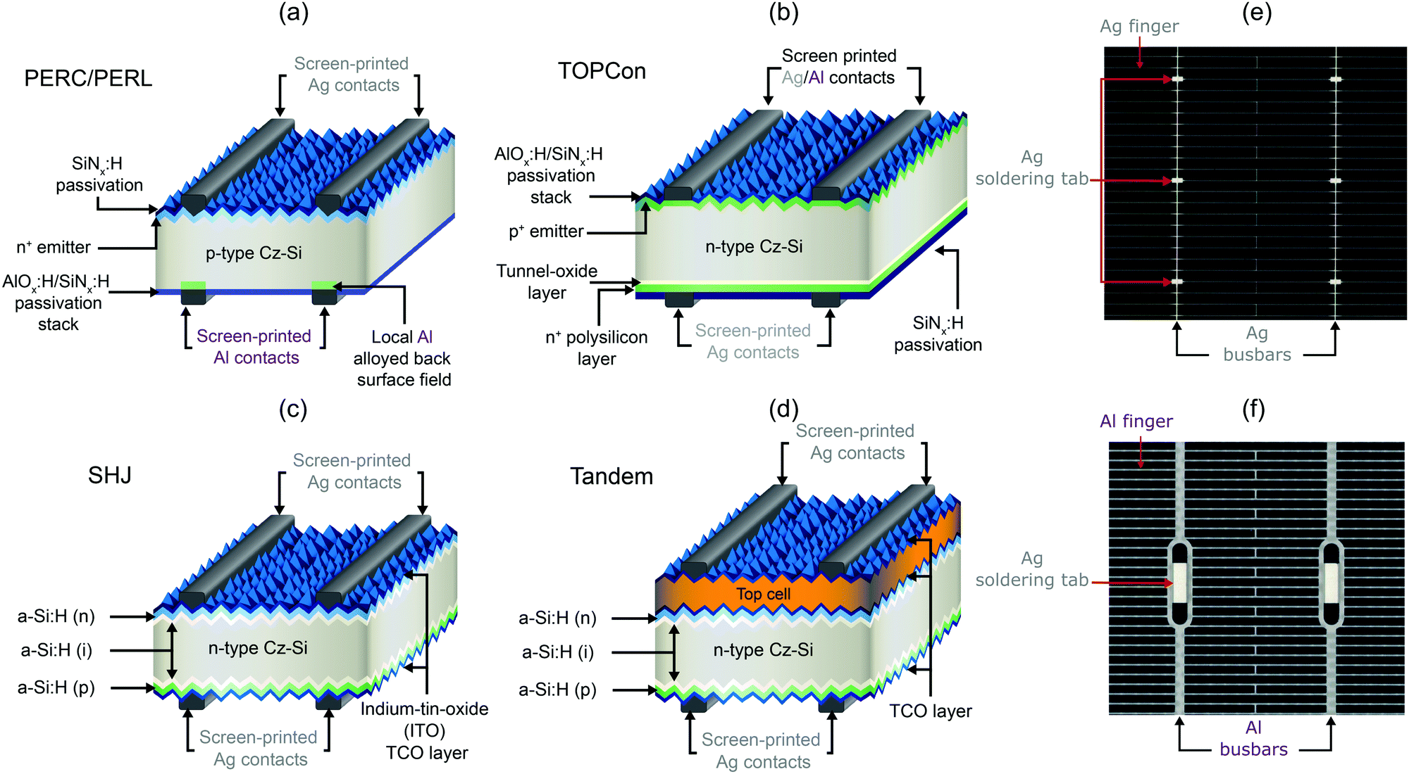 | ||
| Fig. 1 Schematic diagrams of (a) PERC solar cell (b) TOPCon solar cell (c) SHJ solar cell (d) two-junction two-terminal tandem solar cell with SHJ bottom cell. Images of H-pattern grid with (e) Ag fingers, Ag busbars, and Ag soldering tabs (relevant for the front surface of PERC, and both the front and rear contacts of TOPCon and SHJ solar cells). (f) Al fingers, Al busbars, and Ag soldering tabs (relevant for the rear surface of PERC). | ||
On the rear side of PERC solar cells, cheaper and more abundant aluminium is used to form fingers and busbars for bi-facial solar cells (or the entire rear side for mono-facial cells) as shown in Fig. 1(f). In this instance, interactions of aluminium with silicon are advantageously used to form aluminium back-surface field (Al-BSF) at contacted regions, as a simple and low-cost version of that implemented in the world-record PERL cell which reached 25% efficiency.7 Due to a reduced incident illumination intensity on the rear surface, the restrictions of the metal coverage area for optical shading are relaxed. Consequently, much wider (∼100 μm wide) and more closely spaced aluminium fingers can be used to compensate for the lower conductivity of aluminium compared to silver, with an aluminium consumption of ∼200 mg in bi-facial PERC solar cells. However, due to difficulties in soldering to aluminium, additional silver is required to form soldering pads on the rear side for interconnection. This is typically achieved using an Ag paste with 50–60% silver content by weight, compared to 80–90% silver content in Ag pastes used on the front side.50 As such, two printing steps are required for the rear surface. Overall, this results in the consumption of approximately 90–100 mg of silver per PERC solar cell fabricated on 166 × 166 mm2 silicon wafers in 2020,10 corresponding to a silver consumption of approximately 15.4 mg W−1 (see Table 2).
| Cell structure | 2020 | Predictions for 2031 | ||||||
|---|---|---|---|---|---|---|---|---|
| Ag usage (mg per cell) | Eff. (%) | Ag usage (mg W−1) | Percentage of global Ag supply for 1 TW production (%) | Ag usage (mg per cell) | Eff. (%) | Ag usage (mg W−1) | Percentage of global Ag supply for 1 TW production (%) | |
| PERC | 96 | 22.8 | 15.4 | 53 | 57 | 24.5 | 8.5 | 29 |
| TOPCon | 163 | 23.2 | 25.6 | 88 | 95 | 25.0 | 13.8 | 48 |
| SHJ | 218 | 23.5 | 33.9 | 117 | 99 | 25.3 | 14.3 | 49 |
TOPCon and SHJ solar cells are generally considered as promising candidates among academic and industry experts for next-generation high-efficiency industrial solar cells due to the use of ‘passivating contacts’ which overcome the efficiency limitations of conventional contact schemes such as that in PERC and PERL.51 The highest efficiency for a tunnel-oxide passivated contact solar cell stands at 26.1% by Haase et al., also fabricated using a p-type wafer.52 For this solar cell, however, both contacts were on the rear in an interdigitated structure (POLO-IBC). However, a recent result by Richter et al. achieved a record 26% efficiency for a solar cell with contacts on both surfaces.53 This TOPCon solar cell was also fabricated using p-type wafers, slightly higher than the efficiencies achieved by the same group with n-type wafers at 25.8%.54
Industrial TOPCon solar cells are fabricated on n-type wafers, with recent average efficiencies of 23.2% reported by ITRPV, while peak efficiencies as high as 25.25% have been reported by Jinko Solar.55 For industrial n-type TOPCon solar cells, silver pastes are used on both front and rear surfaces, resulting in substantially higher silver consumption than PERC.10 On the front, an Ag/Al paste (∼90% Ag by weight) is used to enable sufficient conductivity in fingers and busbars with a line resistivity of 5–10 μΩ cm to avoid excessive shading and resistive losses, yet also ensuring the formation of high-quality ohmic contacts with the boron-diffused p-type emitters. For the n-type passivated contact on the rear of the device, specially designed silver pastes featuring more controllable etching rates are used to fire through the silicon nitride layer but avoid penetration through the polysilicon and tunnel oxide layers. Both of these pastes are fired at high temperatures, typically in a co-firing process. The estimated silver consumption for TOPCon in 2020 was 25.6 mg W−1, approximately 66% higher than PERC (see Table 2).
The SHJ solar cell technology is responsible for the highest efficiency silicon solar cell at 26.7%, fabricated on n-type wafers with an interdigitated back-contact structure.56 Industrial SHJ solar cells are also fabricated on n-type wafers, however, mostly feature screen-printed contacts on both surfaces. The average efficiency for industrial n-type SHJ solar cells is in the range of 23–24%, although efficiencies as high as 25.26% have been reported by LONGi solar.57
Industrial SHJ solar cells also use silver pastes for contacts on both surfaces. To avoid a severe deterioration of surface passivation quality that can occur for higher temperatures, the processing for SHJ solar cells is typically limited to temperatures below 200 °C.58 As such, a low-temperature silver paste is required for both the front and rear contact of SHJ solar cells, which is cured in the vicinity of 150–200 °C. Due to the restriction of low curing temperatures, SHJ silver pastes contain more silver particles and different solvents, additive, and curing agents than traditional silver pastes to ensure the proper formation and curing of contacts at low temperatures. Due to the low curing temperature, the low-temperature Ag pastes for SHJ solar cells tend to have a higher line resistivity (ρm) in the range of 10–20 μΩ cm,59 which is about a factor of two higher than the ρm of the high-temperature silver pastes that are typically used for PERC and TOPCon solar cells. However, significant progress has been made in improving the electrical properties of the low-temperature cured Ag paste, where a reduced line resistivity of 5–6 μΩ cm or even lower has been demonstrated.59 Due to the need for silver contacts on both sides, higher silver content within pastes, and relatively poor printability of such low-temperature pastes, more silver is required such that the typical silver consumption for an SHJ solar cell is more than double that was used for PERC (see Table 2).
As the efficiency of single-junction Si-based solar cells approaches the intrinsic limit of around 29%,60,61 multi-junction (tandem) devices formed by stacking materials with different bandgaps to absorb light at different wavelengths in the solar spectrum, provides a promising pathway to surpass the efficiency limit imposed by single junction devices. With a tandem structure, solar energy can be harvested and utilized more efficiently by reducing thermalisation energy losses62 from high-energy photons being absorbed by a small-bandgap material (e.g. UV light (>3.1 eV) being absorbed in silicon with a bandgap of 1.12 eV), or the transmission losses of photons with insufficient energy to excite materials with larger bandgaps (i.e. photons with energy below the bandgap). To date, maximum efficiencies of 39.2% (under standard 1-Sun illumination) and 47.1% (under concentrated 143-Suns illumination) have been achieved by a six-junction tandem device fabricated with III–V materials,63 well above the record efficiency of 26.7% achieved by single-junction Si-based solar cells.
Currently, tandem solar cells are being extensively developed in hundreds of different types based on different materials, the number of junctions, fabrication and stacking methods, and also the number of electrical terminals. It remains unknown which types of tandem solar cells will represent the leading and dominant technological pathways in the future. However, two-junction (2J) two-terminal (2T) tandem solar cells with Si-based bottom cells (e.g. PERC, TOPCon, and SHJ) appear to be a promising candidate and are attracting more attention from both industry and academia. A record efficiency of 29.52%12 has been achieved by Oxford PV with a 2J&2T perovskite/Si heterojunction tandem solar cell. Compared with other tandem structures, 2J&2T tandems with Si-based bottom cells may have advantages in relatively simple fabrication process, good compatibility with existing interconnection and module technologies, and could also benefit from the well-established industry of Si-based solar cells and technologies.
In this work, discussions on futuristic tandem solar cells will be focused on 2J&2T tandem fabricated on either PERC or SHJ solar cells. For such tandem solar cells, it remains unclear what metallization technology will be used in the future mass production environment. However, due to constraints on processing temperatures, it is likely that screen-printing of low-temperature cured silver pastes will be more desirable and suitable than using high-temperature co-fired pastes or evaporated metal contacts for the mass production of these tandem cells. The use of screen-printing metallization technology has been successfully demonstrated by Oxford PV on commercial sized 2T perovskite/Si heterojunction tandem solar cell in their 100 MW pilot production line.64,65 Therefore, the silver consumption in the futuristic 2T tandem solar cells will also be assessed and discussed in this work, particularly due to their unique current–voltage characteristics and opportunities to reduce silver consumption.
According to the 2021 ITRPV, over the next decade, cell efficiencies of PERC, TOPCon and SHJ solar cells are expected to continuously improve alongside a gradual reduction in the silver usage per cell. Taking into account the expected cell efficiencies and silver consumption per cell, the silver consumption in mg W−1 is expected to reduce by 50–60% by 2031, which will substantially improve the material sustainability of PERC, TOPCon, and SHJ solar cells. However, TOPCon and SHJ are still expected to have a substantially higher consumption of silver than PERC by 63–68% (see Table 2).
The significantly higher silver consumption of TOPCon and SHJ solar cells than PERC greatly reduces the sustainable manufacturing capacity of the technology for the usage of a given percentage of global silver supply within the PV industry (see Table 2 and Fig. 2). Based on the 2020 cell efficiencies and silver consumption for PERC, TOPCon, and SHJ, each TW of annual production capacity for these technologies would consume 53.1%, 88.3%, and 116.9% of the 2019 global silver supply, respectively. Similarly, despite lower projected silver consumption in 2031 for PERC, TOPCon, and SHJ, each TW of annual production for the cell technologies would still consume 29.3%, 47.6%, and 49.3% of the 2019 global silver supply, respectively.
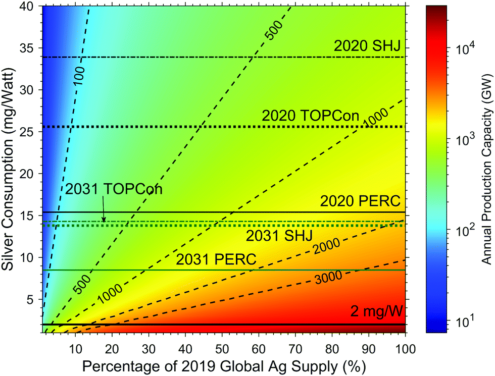 | ||
| Fig. 2 Allowable annual production capacity as a function of the percentage of 2019 global silver supply that can be used in PV manufacturing and silver consumption in mg W−1. Assumptions of efficiencies and silver consumption for PERC, TOPCon, and SHJ solar cells in 2020 and 2031 can be found in Table 2. | ||
To allow a PV manufacturing capacity of 3 TW per annum to fight climate change, Verlinden recently suggested that silver consumption must be reduced to below 5 mg W−1 or lower for all PV technologies to be sustainable,18 which is well below ITRPV predictions in 2031 even for PERC. However, even for 5 mg W−1, an annual production capacity of 3 TW would consume more than 50% of the current annual global silver supply. Considering increasing silver demand from other industries, the sustainable fraction of the silver supply that the PV industry can use, may in fact, be much lower. The exact percentage of global supply that the PV industry can use in the mid to long-term silver consumption is unclear, particularly when accounting for future PV recycling efforts and the expected lifespan of PV modules into the future. However, given the current 25–30 years typical lifetime of commercial solar modules and 20–30% growth rate of the industry, recycling and recovering silver from end-of-life modules will not likely provide significant relief in the pressure of silver supply in short to mid-term.
Fig. 2 shows that if the PV industry can sustainably use 20% of the 2019 global silver supply, this would correspond to a sustainable manufacturing capacity of 227 GW for TOPCon and 171 GW for SHJ compared to 377 GW for PERC based on 2020 efficiency and silver consumption levels. However, silver consumption has reduced substantially over the last decade by a factor of 5 from ∼90 mg W−1. Such reductions in silver consumption are expected to occur into the future with ongoing technology development. With reductions projected by ITRPV in silver consumption in 2031, the allowed manufacturing capacity would increase to around 700 GW of PERC solar cells, ∼420 GW of TOPCon solar cells, or ∼400 GW of SHJ solar cells. As a result, predictions of improvements in current screen-printing metallization technologies by the ITRPV for 2031 are not sufficient to enable manufacturing of PV at the TW or multi-TW level without using much more than 20% of the global silver supply, a value that is likely not sustainable. As shown, SHJ and TOPCon solar cells have approximately half the size of a sustainable manufacturing capacity as PERC. Therefore, from a sustainability perspective, a transition to such technologies is not justified yet for the limited efficiency improvements that industrial TOPCon and SHJ solar cells offer over PERC. However, to allow 3 TW production capacity of PV using only 20% of the global supply, regardless of technology, silver consumption needs to be below 2 mg W−1. With this 2 mg W−1 target, the ITRPV predicted silver consumption in 2031 for PERC, TOPCon, and SHJ solar cells are a factor of 4, 7 and 6 too high to allow a 3 TW manufacturing capacity.
Apart from material sustainability, the LCOE of PV-generated electricity could be at risk due to the dependence on silver. For a typical industrial PERC solar cell, the use of silver already contributes a large portion of the total manufacturing costs (US$0.075 per cell), corresponding to more than 60% of the non-wafer cell price and 6% of the total module cost.10 Therefore, an increase in silver paste price by a factor of two would increase the cost of a PV module by ∼6%. We have to expect that, in the next decade, if no replacement is found for silver in cell manufacturing, the total manufacturing costs of a solar cell and PV module will be strongly affected by the price of silver, which has been quite volatile in the last year.
Historically, the typical cost of capital equipment for manufacturing solar panels has been steadily reducing at a rate of −18% per year over the last decade, benefiting from the scale effect in the PV market, the growing competition in the industry, and continuous technological developments.10 However, this trend does not apply to the price of silver among some other raw materials, where the law of supply and demand generally plays a central role towards the price. Given the growing demand in all industries and the limited reserves and supply of silver, the supply and demand relationship of silver will likely be experiencing more pressure, which could potentially drive the price of silver as well as the manufacturing cost of a solar cell up. Ironically, from the historical point of view, the biggest driving force behind price fluctuations of silver appears to be contributed by the huge volatility in the financial market rather than the law of supply and demand due to the commodity attributes of silver so far. For example, the global financial crisis during 2008 to 2011 resulted in a surging demand for investing in silver to evade the investment risk, driving the price of silver from less than about 350 US$ kg−1 up to almost 1760 US$ kg−1 while the industrial demand has not been changed significantly. A typical PERC solar cell consumes around 80–100 mg of silver with a selling price of US$ 0.78 per cell, corresponding to around 10% of the selling price. But a smartphone normally has a silver consumption of 200–300 mg with a much higher selling price between US$ 400–1500, where the cost of silver only accounts for 0.01–0.05% of the selling price. Consequently, solar cells have a far lower tolerance to any fluctuations in silver price without impacting overall cost. Therefore, the need for silver in solar cells puts the LCOE of PV generated electricity into a more vulnerable position, which can be compromised by possible long-term increases in silver price driven by the growing supply pressure, and the unpredictable short-term volatility in the silver price originated from the global financial market.
As a result, careful consideration of silver consumption within the PV industry will be critical for sustainable PV manufacturing and also protect against potential silver price volatility in the future. The following section discusses the interdependencies between physical geometries of silver metallization contacts, solar cell efficiencies, and the corresponding silver consumption to assess the feasibility of existing and emerging technologies.
Physical constrains in silver reduction in screen-printed solar cells
The physical constraints on the finger dimension and geometry must be taken into account to ensure a feasible and realistic reduction of the silver consumption in fingers when heading towards more sustainable solar cell manufacturing practices for screen-printed solar cells. In this section, we provide limitations in finger geometries based on both a shorter-term target of 5 mg W−1 and a longer-term target of 2 mg W−1.The consumption of silver in screen-printed fingers can be understood simply in terms of finger spacing and cross-sectional area. An upper limit for the allowed silver consumption in fingers for solar cell technologies is given for use with busbar-less interconnection technologies such as the SmartWire approach, whereby silver is only used for fingers. With the SmartWire technology, the conventional silver busbars and soldering tabs are replaced by copper wire coated with low-temperature solders such as tin bismuth and supported by a polymer laminate sheet,66 thereby eliminating silver usage associated with busbars and soldering tabs. The electrical contact between the copper wires and underlying fingers is formed during the module lamination process in the vicinity of 130–170 °C with a melting and re-flow of the low-temperature solder, without the need of a dedicated soldering step in conventional interconnection approaches prior to lamination. In this context, to limit the silver consumption to 5 mg W−1 in finger regions, there is a given allowed finger cross-sectional area for a given finger spacing and device performance. Fig. 3 shows the impact of finger spacing and cross-sectional finger area for a 23.8% efficient PERC cell on the finger silver consumption. Using the current 1.3 mm finger spacing in typical industrial PERC solar cells, the cross-sectional area must be reduced to less than 300 μm2 to reduce finger silver consumption to less than 5 mg W−1, compared to a current value of between 500–600 μm.2 For TOPCon and SHJ solar cells, despite slight increases in efficiency, due to the need for silver fingers on both sides, the maximum allowable finger cross-sectional area for a given silver consumption is substantially smaller than that for PERC. For 24.58% efficient TOPCon solar cells, with a 1.5 mm finger spacing on both sides, the allowed cross-sectional area for fingers would be 170 μm,2 equating to a finger silver usage of 2.5 mg W−1 on each of the surfaces. For the front and rear surface of 25.1% efficient SHJ solar cells with finger spacings of 2 mm and 1 mm, respectively, the allowed cross-sectional area for fingers would be even smaller, at 150 μm2. With a more restricted finger silver usage of 2 mg W−1, both TOPCon and SHJ solar cells would require the finger cross-sectional area to be reduced to 60–70 μm2, comparing to 120 μm2 for PERC solar cells. On the other hand, the significantly increased efficiency potential of tandem solar cells naturally increases the allowed cross-sectional area for a given finger spacing. However, the largest increase in the allowed cross-sectional area of 270 μm2 and 748 μm2 for 2T tandem solar cells comes due to increased front and rear finger spacings of 3 mm and of 1.5 mm, respectively, as will be discussed in the following section on series resistance. With a total finger silver usage of 2 mg W−1, both tandems on SHJ and tandems on PERC could still allow a reasonable finger cross-sectional area of 108 μm2 and 299 μm2, respectively.
 | ||
| Fig. 3 Finger silver consumption for 23.8% efficient PERC cells as a function of front finger spacing and finger cross-sectional area. The wafer area is assumed to be 210 × 210 mm2. The hashed region has the finger silver consumption above the 2 mg W−1 target. Contour lines represent different finger silver consumption levels. | ||
Using PERC structure as the bottom cell in tandem also presents a unique opportunity of preserving Al fingers on the rear side to reduce the silver consumption. However, this will largely depend on the configuration of the top cell among the choice of interconnection layers, where Al fingers can only be used when the n-type diffused emitter of PERC is contacting the top cell. Otherwise, silver fingers are still required on both sides of the tandem device, leading to no significant advantage for tandem on PERC compared to tandem on SHJ in terms of silver consumption. In this work, we assume Al fingers and busbars are used on the rear side of tandem on PERC solar cells.
The choice of the optimal finger spacing is essentially a trade-off between series resistance losses and optical shading losses, in which a larger finger spacing leads to reduced optical shading but increased series resistance losses contributed by finger resistance, lateral resistance within the silicon or conducting layers, and contact resistance. As a result, the trend of using more lightly doped front emitters in PERC and TOPCon solar cells and reductions in finger width with the ongoing development of screen print will very likely point towards a continuously reduced finger spacing in the future compared to that in current industrial solar cells. With a smaller finger spacing, the finger cross-sectional area that can be tolerated by a given finger silver consumption is expected to be even smaller. For instance, as shown in Fig. 3, the use of 1 mm finger spacing instead of 1.3 mm in PERC solar cells will reduce the allowable finger cross-sectional area from 300 μm2 to 230 μm2 for a finger silver usage of 5 mg W−1.
For conventional interconnection technologies, extra silver is required for busbars and soldering pads for the interconnection of cells. This means that to achieve a target value of total silver consumption for the device, the silver consumption in fingers needs to be further reduced to account for the silver consumption required in busbars and solder pads. In the case of using 12 busbars (12BB) per solar cell and 18 soldering pads per busbar, values in the range of 3.7–4.1 mg W−1 are required for busbar and tabbing regions of PERC and Tandem/PERC solar cells, and 4.2–5.0 mg W−1 for TOPCon, SHJ, and Tandem/SHJ solar cell technologies (see Table 3). This would reduce the allowed cross-sectional area of fingers of a challenging 52 μm2 and for PERC. Tandem/SHJ would be restricted to an even more challenging 41 μm2 due to the need for silver busbars and tabs on both surfaces. However, for tandem on PERC, a much more reasonable finger cross-sectional area of 200 μm2 could be tolerated. Due to a busbar and tab silver consumption of almost 5 mg W−1, the option of using 12BB configuration with silver being used in all fingers, busbars, and tabbing regions of SHJ and TOPCon solar cells is clearly unfeasible at the TW scale with a targeting total silver consumption of less than 5 mg W−1. If reduced to a limit of 2 mg W−1, no such technology is feasible with silver being used all finger, busbar and tabbing regions.
| Ag usage (mg W−1) | PERC | TOPCon | SHJ | Tandem on SHJ | Tandem on PERC |
|---|---|---|---|---|---|
| Front fingers | 8.63 | 8.91 | 6.87 | 3.95 | 4.28 |
| Front busbars | 1.71 | 1.76 | 1.72 | 1.48 | 1.60 |
| Front tabs | 0.88 | 0.75 | 0.74 | 0.64 | 0.69 |
| Rear fingers | — | 8.91 | 13.74 | 7.91 | — |
| Rear busbars | — | 1.76 | 1.72 | 1.48 | — |
| Rear tabs | 1.55 | 0.75 | 0.74 | 0.64 | 1.38 |
| Fingers total | 8.63 | 17.81 | 20.62 | 11.86 | 4.28 |
| Busbars total | 1.71 | 3.52 | 3.44 | 2.96 | 1.6 |
| Tabs total | 2.43 | 1.51 | 1.48 | 1.27 | 2.06 |
| Total | 12.78 | 22.83 | 25.52 | 16.09 | 7.94 |
On the other hand, if non-silver busbars are used, such as copper or aluminium, a relaxation on the silver consumption could be enabled in fingers while still ensuring compatibility with standard soldering techniques through the use of silver tabbing regions. In this instance, 2.1–2.4 mg W−1 is used for the tabbing regions of PERC and tandem/PERC devices, and 1.3–1.5 mg W−1 is used for TOPCon, SHJ, and Tandem/SHJ solar cells. A target of 5 mg W−1 for the entire device would limit the allowed finger cross-sectional area for PERC to 160 μm2, SHJ and TOPCon to 100–120 μm2, and a more manageable value of 200–440 μm2 for Tandem/SHJ and Tandem/PERC. If reduced to 2 mg W−1 for the total device, no such technology appears feasible with a 12BB design, even for Tandem/PERC with an allowed cross-sectional area of 43 μm2.
A summary of the allowable finger cross-sectional area of various solar cell structures in different scenarios can be found in Fig. 4, of which the shaded regime represents the cross-sectional area that we consider to be technologically unfeasible or very challenging with existing screen-printing technologies, which we assume as below 100 μm2. With the smallest finger width current being demonstrated with screen printing of 20 μm,67 a cross-sectional area of less than 100 μm2 would essentially require the average finger height to be reduced to less than 5 μm. Given the typical height of textured pyramids of 1–3 μm, such a low printed height could raise significant concerns about the printability and reliability of such fingers.
 | ||
| Fig. 4 Allowable finger cross-sectional area for various solar cell technologies with different finger silver consumption. The assumed cell area is 210 × 210 mm2. Assumed efficiencies of PERC, TOPCon, SHJ, tandem on SHJ, and tandem on PERC are 23.83%,9 24.58%, 25.11%, 29.15%, and 27.70%, respectively. Filled circles: total 5 mg W−1 silver consumption with silver being used in fingers, busbars, and tabs. Filled triangles: total 5 mg W−1 consumption with silver being used in fingers and tabs. The hashed region has the allowable finger cross-sectional area less than 100 μm. | ||
With a limited silver consumption of 5 mg W−1 for the whole device, the use of 12 silver busbars, as in current industrial solar cells, cannot be tolerated, as using silver busbars will likely reduce the allowable finger cross-sectional area to well below 100 μm2 for PERC, TOPCon, SHJ, and tandem/SHJ solar cells as shown in Fig. 4. However, one notable exception is tandem/PERC solar cell, for which 5 mg W−1 silver consumption could be sufficient for silver fingers, busbars, and tabs. For a more restricted silver consumption of 2 mg W−1, neither silver busbars nor tabs can be used in any of these cell structures based on the current lay-down of silver in busbar and tabbing regions if silver fingers are also used. In addition, even if all 2 mg W−1 of silver were used in fingers, TOPCon and SHJ solar cells would still require the finger cross-sectional area to be reduced to around 60 μm2, and the allowable finger cross-sectional area of PERC and tandem/SHJ is only slightly larger than 100 μm2.
An area of critical research will be on understanding the impact of greatly reduced cross-sectional areas of screen-printed fingers on the performance yield and printing reliability of solar cells in mass production. A recent study by Chen et al. indicated that for a 5-busbar design with 155 fingers, an optimal cross-sectional area of 300 μm2 should be targeted, below which the efficiency would decrease.68 However, this number can likely be reduced for a higher number of busbars such as with the multi-busbars (MBB) technology currently gaining popularity in the industry, of which 9 (or even more) narrow busbars are used with small soldering tabs to replace the traditional 3-busbar or 5-busbar configuration.69 In addition, state-of-the-art stencil printing in the laboratory68 has achieved a cross-sectional area of approximately 200 μm2 for a finger width of 20 μm, which is well above the allowed cross-sectional area for many of the configurations presented in Fig. 4.
Silver consumption can also be considered using parameters such as the coverage area and average printed height. Fig. 5 shows the correlation between the coverage area and printed height on the silver consumption in a typical industrial PERC solar cell. Here it is assumed that all parts of the device (i.e., fingers, busbars, and solder tabs) have the same printed height. An upper limit of the front metal coverage area for PERC could be assumed for the case of 35 μm wide fingers with a finger spacing of 1 mm and also using silver for busbars and tabs in a 12BB design. As such, an upper limit of the coverage area would be 6.13%. In this instance, the average printed height must be below 4.7 μm or 1.9 μm to limit front surface silver to 5 mg W−1 or 2 mg W−1, respectively. On the other hand, a lower limit for the coverage area with continuous silver fingers would be considered as using 20 μm wide fingers, as recently demonstrated in laboratory,70 with a 1.3 mm finger spacing in conjunction with a busbar-less design. In this instance, the lower limit of the coverage area is 1.54%. For this, the average printed height must be below 15.2 μm and 6.1 μm for a total front surface silver consumption of 5 mg W−1 and 2 mg W−1, respectively. For SHJ/TOPCon, which requires silver on both surfaces, 35–40 μm wide fingers and the use of existing 12 busbars and soldering tabs configuration result in a coverage area of 2.15% and 3.48% on the front and rear surface for SHJ, and 3.35% on both surface for TOPCon. As such, to limit the total silver consumption to 5 mg W−1 and 2 mg W−1, the allowed printed height is below 3.1 μm and 1.2 μm for SHJ, and 3.4 μm and 1.4 μm for TOPCon, respectively. The requirement of substantially reduced printed height will likely raise significant concerns in terms of the printability and reliability of such fingers in the mass production environment, especially as the printed height approaches or becomes lower than the height of textured pyramids. Although the minimum printed height can be tolerated in mass production remains unknown and will be an area of critical research, reducing the printed height will likely increase the chance of having broken fingers and damage to screens with thinner emulsion.
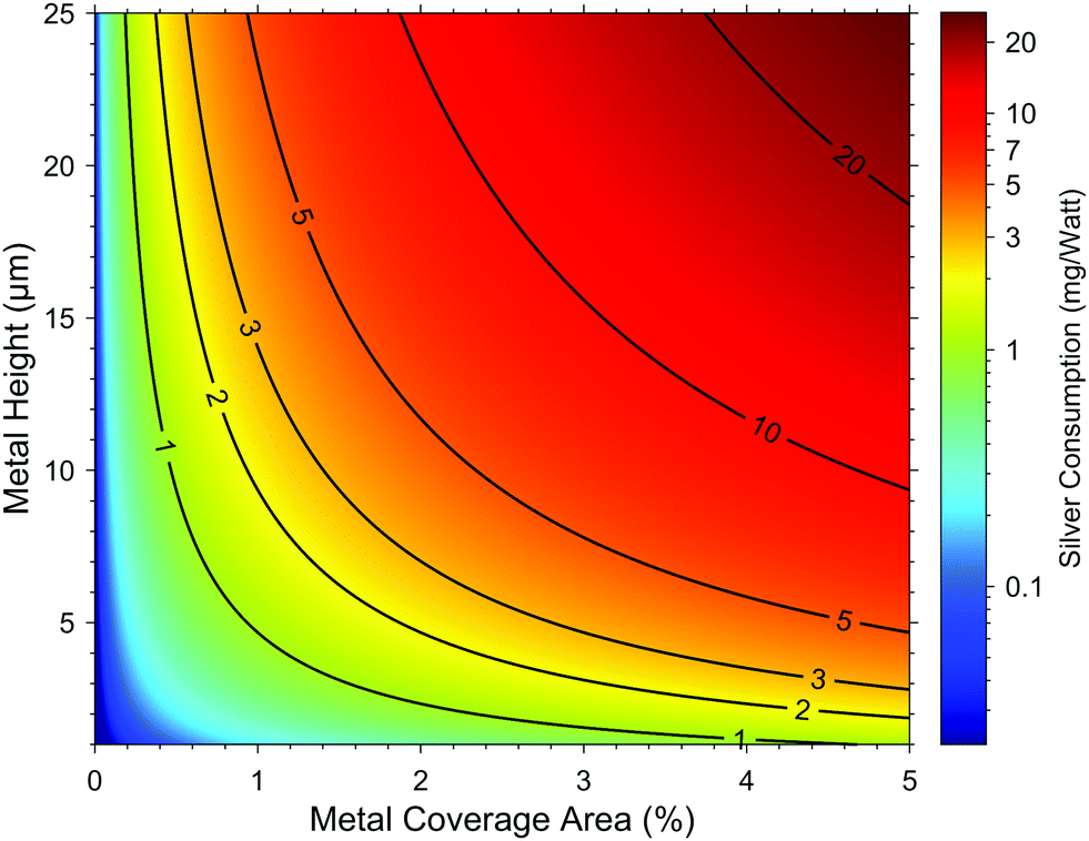 | ||
| Fig. 5 Silver consumption as a function of printed metal coverage area and height in typical PERC solar cells. The assumed cell efficiency and the area are 23.83% and 210 × 210 mm2. Contour lines represent different silver consumption levels. | ||
If the coverage area could be reduced to 1%, a substantial increase in the printed height would be allowed. Table 4 summarizes the coverage area for different solar cell structures and a breakdown of regions such as fingers, busbars, and tabs. As shown, the busbars and tabs of a 12BB structure account for 0.57% of the coverage area in PERC, and 1.14% in SHJ/TOPCon, which rules out the option of using silver busbars and tabs if the coverage area were limited to 1%. However, even with busbar-less interconnection, 1% of the finger coverage area would require the finger width to be reduced to less than 13 μm for PERC with 1.3 mm finger spacing, 7.5 μm for TOPCon with 1.5 mm finger spacing, and 6.7 μm for SHJ with 2 mm and 1 mm finger spacing on the front and the rear, well below the minimum finger width currently being achieved for continuous silver fingers with screen print in industry and laboratory. Therefore, innovation in the finger pattern, such as the use of intermittent silver fingers or development in new printing technologies, is required to achieve a finger coverage area of 1%. Alternatively, a lower metal coverage area, if using the same print height, would enable significant silver savings. For example, with a total coverage area of 1% and an average print height of 5 μm, the silver consumption for the front surface of PERC would be only 1.1 mg W−1, providing scope for innovation to enable sustainable TW manufacturing for screen printed PERC solar cells, without the need to transition to alternative metallization technologies.
| Metal coverage | PERC | TOPCon | SHJ | |
|---|---|---|---|---|
| Front surface | Finger area (%) | 2.69 | 2.53 | 2.00 |
| Busbar area (%) | 0.57 | 0.57 | 0.57 | |
| Tab area (%) | 0.29 | 0.24 | 0.24 | |
| Rear surface | Finger area (%) | — | 2.53 | 4.00 |
| Busbar area (%) | — | 0.57 | 0.57 | |
| Tab area (%) | 1.76 | 0.24 | 0.24 | |
| Total Ag coverage area (%) | 5.32 | 6.70 | 7.63 | |
Impact of silver reduction on finger series resistance losses
One of the key functions of silver in all industrial solar cells is conducting electricity along the fingers to the busbars for current extraction. In general, solar cell fingers are primarily of uniform composition along the length of the finger in terms of width (Wf) and height (tf), and a uniform spacing is provided between fingers (Sf) as shown in Fig. 6. In this case, the differential resistive power losses on fingers are governed by eqn (1) below, where x and ∂x represent the position and the width of the differential component along the length of fingers, Jmp is the current density of the cell at the maximum power point, Sf is the finger spacing, and ρm is the line resistivity of fingers.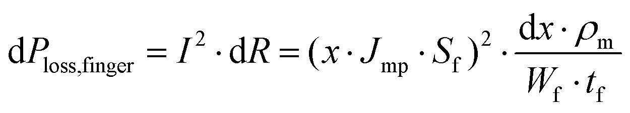 | (1) |
 | ||
| Fig. 6 Schematic diagram of busbars and fingers in the conventional H-pattern grid. | ||
By integrating eqn (1), the absolute and relative power loss (Plossfingerresist;rel) from the finger series resistance can be expressed in the form of eqn (2) and (3), respectively. Both absolute and relative power losses from finger series resistance exhibit an inverse linear dependency on the cross-sectional area of fingers (Wf × tf). With increased busbar spacing (SBB), the current is required to travel over a longer distance along fingers, leading to higher finger resistance losses. The use of a larger finger spacing for a given finger cross-sectional area would also increase finger resistance losses due to increases in the amount of current being collected and transported by each finger.
 | (2) |
 | (3) |
 | (4) |
 | (5) |
 | (6) |
However, in this form, the dependence of finger resistance losses on silver consumption in eqn (3) is not so apparent. The silver consumption in mg (MAg) due to fingers on a solar cell is given by eqn (4), where ρf is the mass density of fingers, and fAg is the fraction of solid Ag content in fingers. The busbar spacing can also be expressed in terms of the cell width (Wcell) and the number of busbars (NBB), as shown in eqn (5). A new expression of relative finger resistance power losses (eqn (6)) can be obtained by combining eqn (3)–(5). A key conclusion from eqn (6) is that with uniform fingers, as is essentially the case for industrial silicon solar cells, the relative power losses from the finger series resistance can be clearly defined by the number of busbars, line resistivity, and the total mass of silver being used in fingers, MAg. That is, an identical consumption of a given paste (i.e., identical MAg and line resistivity) and the same number of busbars will result in the same relative power losses from finger series resistance, regardless of finger spacing and geometry (cross-sectional area). As such, efforts to reduce finger silver consumption by 50% will lead to a doubling of the relative finger series resistance power losses. The relative finger resistive loss also has an inverse square dependence on the number of busbars. As such, this favours the use of interconnection technologies with a higher number of busbars (e.g., MBB technology) as an effective solution to counteract increased finger resistive losses caused by reductions in finger silver consumption. For example, the transition from a 9BB to an 18BB configuration would allow a reduction in the finger silver consumption by a factor of four without increasing finger resistive losses. Fig. 7 shows the relative power losses from the front finger series resistance of a typical PERC solar cell, assuming an efficiency of 23.8%, as a function of the silver consumption in the fingers and the number of busbars.
 | ||
| Fig. 7 Relative power losses from the front finger series resistance as a function of the finger silver consumption and the number of busbars in PERC solar cells assuming an efficiency of 23.8%, cell area of 210 × 210 mm2, line resistivity of 5 μΩ cm, silver paste density of 6 g cm−3, and fractional silver content in fingers of 85%. Dashed contour lines mark relative power losses from finger series resistance. | ||
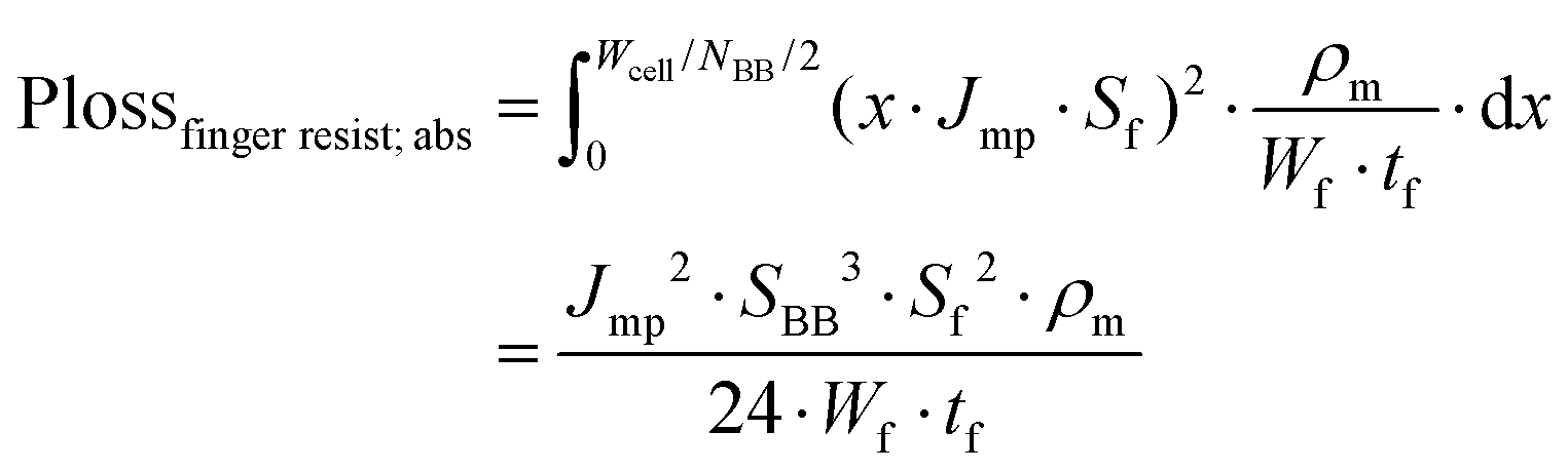
Another striking feature of eqn (6) is the dependence of finger resistance losses on the Jmp/Vmp ratio, hence favouring solar cell technologies with high voltage and low current density output. Table 5 shows values of the cell performance and Jmp/Vmp ratios for a range of solar cell technologies, including PERC, TOPCon, SHJ, and Tandems. As shown, TOPCon and SHJ allow a reduction in the Jmp/Vmp ratio of ∼10% and 8–15% compared to PERC, respectively. As such, assuming an identical grid design with the same line resistivity, resistive losses of TOPCon and SHJ will be 10% and 15% lower than PERC, respectively. However, the most noticeable reduction in the Jmp/Vmp ratio comes from tandem solar cells. Specifically, tandem devices are composed two solar cells with different materials with different bandgaps. The top cell has a larger bandgap (ideally in the range of 1.6–1.8 eV71,72) and absorbs the shorter-wavelength part of the solar spectrum, while the bottom cell has a smaller bandgap (ideally in the range of 0.9–1.2 eV71,72) to absorb the longer-wavelength part of the solar spectrum. An example of JV curves and external quantum efficiency (EQE) of an industrial PERC solar cell and a 2J&2T tandem solar cell73 can be found in Fig. 8. Because the two cells are connected in series in the tandem device, and each absorbs the photon-weighted half of the solar spectrum, the generated current is half of that in a single-junction silicon solar cell. In addition, due to the series connection of two cells and that the bandgap and therefore voltage of the top cell is almost twice that of the bottom cell, the output voltage of such 2J&2T tandem solar cells will be increased by a factor of around 3 compared to that of a typical single junction silicon solar cell, leading to a 5–6 times reduction in the ratio of Jmp/Vmp, as also shown in Table 5. Therefore, 2T tandem solar cells are expected to have substantially reduced finger series resistance losses and could provide significant scope for reducing silver consumption in fingers, and hence improved sustainability compared to single junction solar cells.
| η (%) | V OC (V) | J SC (A cm−2) | FF (%) | J mp (A cm−2) | V mp (V) | J mp/Vmp (A cm−2 V−1) | Ref. | |
|---|---|---|---|---|---|---|---|---|
| PERC | 23.83 | 0.688 | 0.0418 | 82.83 | 0.0398 | 0.599 | 0.0664 | 9 |
| 23.39 | 0.690 | 0.0412 | 82.26 | 0.0389 | 0.601 | 0.0645 | 40 | |
| 22.02 | 0.679 | 0.0399 | 81.31 | 0.0379 | 0.580 | 0.0655 | 123 | |
| TOPCon | 24.58 | 0.717 | 0.0406 | 84.52 | 0.0384 | 0.640 | 0.0600 | 124 |
| 25.09 | 0.720 | 0.0416 | 83.83 | 0.0397 | 0.632 | 0.0632 | 125 | |
| 26.00 | 0.732 | 0.0421 | 84.30 | 0.0402 | 0.647 | 0.0622 | 53 | |
| 23.22 | 0.712 | 0.0411 | 79.29 | 0.0385 | 0.603 | 0.0638 | 126 | |
| SHJ | 25.11 | 0.747 | 0.0396 | 84.98 | 0.0377 | 0.667 | 0.0565 | 127 |
| 23.48 | 0.734 | 0.0392 | 81.77 | 0.0374 | 0.628 | 0.0596 | 128 | |
| 23.70 | 0.745 | 0.0394 | 80.90 | 0.0369 | 0.643 | 0.0573 | 129 | |
| Tandem on PERC | 23.00 | 1.732 | 0.0165 | 79.00 | 0.0159 | 1.442 | 0.0110 | 130 |
| 22.80 | 1.750 | 0.0176 | 73.80 | 0.0161 | 1.420 | 0.0113 | 131 | |
| Tandem on SHJ | 29.15 | 1.900 | 0.0193 | 79.52 | 0.0179 | 1.630 | 0.0110 | 73 |
| 25.24 | 1.788 | 0.0195 | 73.10 | 0.0178 | 1.422 | 0.0125 | 97 | |
| 27.14 | 1.886 | 0.0191 | 75.30 | 0.0174 | 1.559 | 0.0112 | 132 |
 | ||
| Fig. 8 JV curves and external quantum efficiencies (EQE) of a typical 21.9% efficient industrial PERC solar cell (black), a 28.1% efficient two-junction two-terminal Si-based tandem solar cell73 (red), the top (blue) and the bottom cell (green) of the same tandem device. | ||
Fig. 9 shows the relative power losses for finger series resistance as a function of the Jmp/Vmp ratio and bulk resistivity of the metal paste assuming a constant number of busbars (12BB) and fixed cross-sectional finger area and finger spacing of 640 μm2 and 1 mm, respectively. Bands of Jmp/Vmp ratios are shown for PERC, TOPCon, SHJ, and tandem devices according to the IV properties in Table 5, along with a range of values for the bulk resistivity of typical screen-printed Ag, Al, and Cu pastes and bulk resistivity values of the pure Ag. Cell technologies with a lower ratio of Jmp/Vmp not only have potential in more silver reduction and less finger resistance losses but also could have better tolerance to materials with higher line resistivity. For example, assuming the same finger spacing, a slightly lower Jmp/Vmp ratio of TOPCon and SHJ solar cells could allow a 10–15% increase in the finger line resistivity without increasing the finger resistance losses compared to PERC solar cells. As for tandem solar cells, similar finger resistance losses of PERC solar cells with existing Ag pastes could be achieved on tandem devices with much more resistive but low-cost and abundant Cu pastes, enabling an additional pathway of reducing silver consumption in tandem solar cells.
 | ||
| Fig. 9 Relative finger resistance losses with different ratio of Jmp/Vmp and line resistivity of fingers. The same metallization pattern (1 mm finger spacing with 12 busbars) is assumed for all data points. Solid contour lines represent relative power losses from finger series resistance. | ||
The relative finger resistance power losses as a function of finger silver consumption in various cell structures are shown in Fig. 10. It should be noted that for TOPCon, SHJ, and tandem on SHJ solar cells, an even distribution of silver on the front and rear side fingers is assumed, which results in the calculated finger resistance lose values being the lower limit for a given total finger silver consumption. In addition, values for PERC and tandem on PERC only account for resistance power losses from front silver fingers. Nevertheless, owing to the lower Jmp/Vmp ratio and larger finger spacing, we estimate that tandem on SHJ will not only have significantly lower finger silver consumption than existing TOPCon and SHJ due to a much larger finger spacing used but also with much lower finger resistance losses. For tandem on PERC solar cells, we expect a finger silver consumption of less than 5 mg W−1 can already be achieved with current industrial screen-printing technologies with a finger width of 40 μm, finger height of 16 μm, and a finger spacing of 3 mm. In addition, despite the finger silver consumption of only 4.3 mg W−1, the finger resistance loss in tandem solar cells is estimated to be around 0.07%rel, which is 3 times lower than that of current industrial PERC solar cells (0.21%rel) but with twice less finger silver consumption.
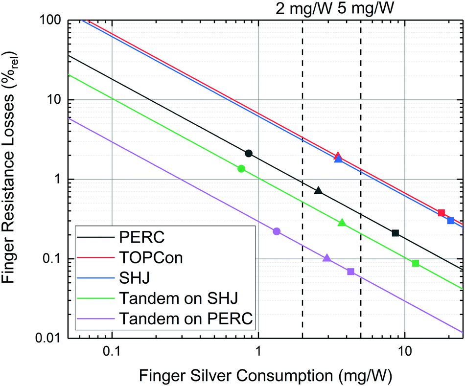 | ||
| Fig. 10 Relative finger resistance losses as a function of finger silver consumption in various cell structures. All values are calculated for the 12BB configuration on 210 × 210 mm2 cells. Assumed efficiencies of PERC, TOPCon, SHJ, tandem on SHJ, and tandem on PERC are 23.83%, 24.58%, 25.11%, 29.15%, and 27.70%, respectively. Filled squares: estimated losses with the current metallization design as shown in Table 3. Filled circles: total 5 mg W−1 consumption with silver being used in fingers, busbars, and tabs. Filled triangles: total 5 mg W−1 consumption with silver being used in fingers and tabs. | ||
A summary of the estimated relative finger series resistance power loss for different technologies is shown in Table 6 for cases of 5 mg W−1 and 2 mg W−1 total silver consumption. As shown, even if extremely small cross-sectional areas or print heights are technically feasible, the lower silver consumption in fingers for various configurations will result in prohibitively high series resistance power losses. This will likely place strict limitations on the lowest silver usage that can be allowed for a given device.
| PERC | TOPCon | SHJ | Tandem on SHJ | Tandem on PERC | |||
|---|---|---|---|---|---|---|---|
| Efficiency | 23.839 | 24.58124 | 25.11127 | 29.1573 | 27.70133 | ||
| Current | Finger silver usage (mg W−1) | 8.63 | 17.81 | 20.62 | 11.86 | 4.28 | |
| Finger Rs loss (%rel) | 0.21 | 0.38 | 0.30 | 0.09 | 0.07 | ||
| Fingers only | 5 mg W−1 | Finger silver usage (mg W−1) | 5.00 | 5.00 | 5.00 | 5.00 | 5.00 |
| Finger Rs loss (%rel) | 0.36 | 1.34 | 1.24 | 0.21 | 0.06 | ||
| 2 mg W−1 | Finger silver usage (mg W−1) | 2.00 | 2.00 | 2.00 | 2.00 | 2.00 | |
| Finger Rs loss (%rel) | 0.91 | 3.36 | 3.10 | 0.52 | 0.15 | ||
| Fingers + tabs | 5 mg W−1 | Finger silver usage (mg W−1) | 2.57 | 3.49 | 3.53 | 3.73 | 2.94 |
| Finger Rs loss (%rel) | 0.71 | 1.93 | 1.76 | 0.28 | 0.10 | ||
| 2 mg W−1 | Finger silver usage (mg W−1) | — | 0.49 | 0.53 | 0.73 | — | |
| Finger Rs loss (%rel) | — | 13.63 | 11.69 | 1.42 | — | ||
| Fingers + 12BBs + tabs | 5 mg W−1 | Finger silver usage (mg W−1) | 0.86 | — | — | 0.76 | 1.33 |
| Finger Rs loss (%rel) | 2.11 | — | — | 1.36 | 0.22 | ||
| 2 mg W−1 | Finger silver usage (mg W−1) | — | — | — | — | — | |
| Finger Rs loss (%rel) | — | — | — | — | — | ||
For SHJ and TOPCon solar cells, even with a silver-free interconnection scheme (no silver being used in busbars or tabbing regions), the relative power loss will be in the range of 1.2–1.3% and 3.1–3.4% for a total silver consumption target of 5 mg W−1 and 2 mg W−1, respectively. If also using silver in tab regions, these values increase to 1.7–1.9% and 11.7–13.6%, respectively. Such values would be prohibitively high for solar cells. The transition towards silver-free interconnection schemes with a higher number of busbars or wires can effectively reduce losses from finger resistance in TOPCon and SHJ solar cells, however, a minimum of 27 or 75 wires will be required, for a target total silver consumption of 5 mg W−1 and 2 mg W−1, to maintain the same finger resistance losses as current industrial cells with 12 busbars. As for PERC solar cells, finger consumption of 5 mg W−1 not only will not allow the use of silver in all fingers, busbar, and tabs from physical constraints perspective as discussed in the previous section, the finger resistance loss will also be significantly increased from 0.21% to 2.11%, which will lead to a ∼0.5%abs efficiency loss with a current 12-busbar configuration.
Among all cell technologies, tandem on PERC exhibits the greatest potential of achieving low silver consumption but also low finger resistance losses. With 5 mg W−1 of silver being used in fingers, busbars, and soldering tabs, a very low finger resistance loss of 0.22%rel can still be expected for tandem on PERC solar cells. However, technical challenges likely remain regarding integration with the high-temperature metallization for the rear of PERC and the low-temperature requirements for many top cells such as perovskites.
Prospects for silver reduction
Considering the above physical limitations and impact of silver reductions on finger series resistance power losses for screen-printed solar cells, the development and deployment of novel screen-printing methods to reduce silver consumption and alternative silver-free metallization and interconnection technologies must be accelerated to enable sustainable manufacturing at the TW scale.For screen-printed solar cells, the MBB technology, as it is done today with 12 busbars for a 210 mm solar cell, will not be feasible for manufacturing at the TW scale for PERC, TOPCon, and SHJ due to silver consumption of more than 4 mg W−1 in the busbar and tabbing regions alone for all of them. One option is reducing the number of busbars, which is normally undesirable in a solar cell due to increased finger resistance losses. However, with a strictly limited silver consumption level, reducing the number of busbars (assuming unchanged busbar width) will allow more silver to be used to form fingers, which may in fact, lead to lower finger resistance. In addition, the maximum allowable finger cross-sectional area will also be increased by reducing the number of busbars, which improves the reliability and printability of such fingers in the mass production environment. For instance, if the number of busbars in a tandem on SHJ solar cell can be reduced from 12 to 9 on a 210 mm cell (assuming busbar width unchanged), the allowable finger silver consumption will substantially increase from 0.76 mg W−1 to 1.85 mg W−1 with a total silver consumption of 5 mg W−1. Subsequently, a lower finger resistance loss of 1.01%rel and a more manageable finger cross-sectional area of 98.5 μm2 will be allowed, comparing to a finger resistance loss of 1.65%rel and a finger cross-sectional area of 41.3 μm2 if 12 busbars are assumed. Alternatively, tandem solar cells can tolerate greatly reduced paste conductivities to more readily allow the use of non-silver fingers and busbars.
The development and deployment of non-silver busbars (e.g., Al or Cu) or ‘busbar-less’ technologies must be explored for their potential to reduce silver consumption in conventional busbar and tabbing regions, provided that they don’t introduce additional material limitations. However, even with all silver only being used for fingers, achieving a long-term target of 2 mg W−1 will still be challenging with the finger design currently being used in the industry, especially for TOPCon and SHJ solar cells. A finger silver consumption of 2 mg W−1 would only allow a finger cross-sectional area of 120 μm2 for PERC and around 60 μm2 for both TOPCon and SHJ, comparing with 500–600 μm2 in current industrial solar cells. In addition, an equation linking the direct impact of silver consumption on the relative power loss due to series resistance in the fingers highlights that such a dramatic reduction in finger silver consumption will lead to substantially higher finger resistance losses, where a 4-times increase is expected for PERC, and ∼10 times for TOPCon and SHJ solar cells. With this in mind, we cannot rely simply on pure silver fingers for the conduction of carriers to the busbars. Alternative materials or finger geometry and pattern must be developed to accelerate the reduction of silver consumption in fingers allowing a total silver consumption below 5 mg W−1 or even 2 mg W−1. One potential path is using a print-on-print approach with a seed layer of a silver paste to form metal-silicon interface areas, capped by a non-silver conductor. Another approach will be using intermittent silver finger regions to form the metal/silicon interface and relying on non-silver conductors to connect the intermittent regions and provide lateral conduction to the busbars. This will overcome limitations based on the printing width capabilities of screen printing, and simultaneously allow greater reductions in silver consumption.
Another route for reducing silver consumption that must be seriously considered by the PV industry for existing and future technologies is copper plating. Despite reported challenges related to adhesion and reliability,74 solar cell technologies incorporating copper plating have already been successfully deployed for large-scale production by numerous companies. For example, BP Solar used copper plating for its Saturn® technology from 1992–2006,75,76 based on the UNSW buried contact solar cell. A recent study highlighted field performance after 12 years of operation in the field, noting comparable durability with standard screen-print solar cells.77 Suntech's Pluto technology also used plating and was scaled to 500 MW in the period of 2009–2013.78,79 This approach was responsible for the world's first p-type commercial solar cell with an efficiency of over 20%.78 Plating has also been successfully deployed for solar cells with passivated contacts, highly relevant for today's emerging industrial solar cells featuring passivated contacts,80 namely TOPCon and SHJ. For example, Tetrasun's Tetracell technology used plated contacts on top of passivation layers.81 Similarly, Sunpower's Maxeon back-contact technology uses copper plating.82,83 SHJ solar cells with plated contacts have already been deployed by GS Solar.59 There is increasing interest in the academic community for plating on both TOPCon and SHJ solar cells, for example see ref. 84–86. The use of copper as a replacement for silver at the cell level would have a negligible increase to the overall copper consumption for PV technologies.
In all instances, futuristic tandem devices have a unique opportunity to greatly reduce material consumption, including silver, far beyond that achievable with existing technologies in mass production such as PERC, TOPCon, and SHJ solar cells. Due to the low Jmp/Vmp ratio and a strong dependency of finger resistance power losses on the ratio of Jmp/Vmp, the tandem cell can better tolerate a reduced number of busbars or reduced finger cross-sectional area without significantly impacting series resistance, which will subsequently enable a considerable reduction in silver consumption in tandem devices.
Prospects for emerging module technologies
In addition to advancements in cell technologies, several new interconnection approaches and module technologies, such as SmartWire, half-cell, and shingled modules have been developed to improve the efficiency/output power at the module level and are currently gaining increasing attention from the industry. With a higher output power, the mg W−1 consumption of silver at the module level is naturally reduced. However, due to relatively small increases in power, the sustainable manufacturing capacity of PV modules is not expected to significantly increase. On the other hand, some of these module technologies could provide unique opportunities for considerable silver reductions on the cell level.With the SmartWire technology, the interconnection between cells is achieved by copper wires coated with low-temperature solders directly contacting with fingers,66 which eliminate the usage of silver in traditional busbars and tabbing regions. In addition, the increased number of wires commonly featured in the SmartWire configuration66 could provide greater tolerance to a reduced finger silver consumption or increased finger resistivity for the use of other materials (e.g. Al or Cu) without causing excessive increases in finger resistance losses. However, the additional usage of other scarce metals, specifically bismuth in the low-temperature solders, needs to be evaluated carefully to ensure no outstanding concerns will be raised by the availability and supply of bismuth for the SmartWire technology.
The concept of half-cell modules, as suggested by their name, is essentially having pre-cut half cells rather than full-area cells in the module. Due to the use of half-cell, the amount of current of each string in a module is effectively halved, leading to a significant reduction in the power loss of series resistance,87 which is governed by the relationship of Ploss = I2 × R. However, it should be noted that the amount of current collected by and traveling within each finger remains to be unchanged with the half-cell configuration, resulting in finger series resistance power losses the same as in full-cell modules. As such, half-cell modules do not have significant advantages over full-cell modules on reducing the silver consumption in fingers. In addition, the interconnection of half-cell modules relies on the conventional soldering process, of which busbars and soldering tabs are still needed, providing no obvious scope of silver reductions in those regions.
For shingled modules, each full-area solar cell is cleaved into 5 or 6 strips (also known as shingles), and those strips are ‘shingled’ together like roof tiles on the long edge and bonded with an electrically conductive adhesive (ECA).88,89 This approach eliminates the need of a conventional soldering process as well as the gap between each cell that is normally required in most ribbon-connected modules. As such, the packing density can be improved, and optical shading losses from busbars, soldering tabs and ribbons can be avoided. Due to the omission of the soldering process, silver soldering tabs are no longer needed in shingled modules. In addition, it is possible to replace conventional busbars with localized Ag pads90,91 or use busbar-less solar cells in a shingled module,92,93 especially with SHJ solar cells, of which the conductivity of ITO layers on both sides could also contribute to the current transport between shingles. Therefore, the shingled configuration presents a unique opportunity to considerably reduce the silver consumption in busbars and soldering tabs regions. However, attention must also be paid to the silver consumption of the ECA if Ag particles or Cu particles coated with Ag layers were used as the filling material. Since normally a few grams of ECA will be printed or dispensed on each shingle, the percentage content of silver in ECA needs to be limited to a very low level to avoid any excessive increases in silver usage. Therefore, careful evaluation between the silver content and electrical properties, mechanical properties, and reliabilities is of vital importance to the shingling technology. Meanwhile, other cheaper and more abundant materials should also be explored for ECAs.
On the other hand, within the shingled solar cells, the finger length for current to travel is substantially longer than that in conventional full cells with 9BB, resulting in significantly higher finger series resistance losses in shingled modules. For example, if each full cell was cleaved into 6 shingles, the finger length of each shingle is equivalent to that in a 3-busbar solar cell and is three times longer than that in a conventional 9-busbar solar cell, leading to a 9-fold increase in finger series resistance losses as shown in eqn (3). In this instance, reducing the finger silver consumption will become more challenging in current shingled design with silver fingers due to undesirably high-power loss from finger series resistance. For example, as was shown in Fig. 7, this would increase the power loss from a 9BB PERC solar cell from 0.57% and 1.12% to 5.13% and 10.08% for shingled solar cells (6 shingles) assuming a finger silver consumption of 5 mg W−1 and 2 mg W−1, respectively.
Indium consumption in PV industry
In the PV industry, indium is predominately used in the form of indium-tin oxide (ITO) as a transparent conductive oxide layer (TCO) for SHJ solar cells. In-based alloys have also historically been used for low-temperature soldering and interconnection technologies such as SmartWire.66 However, due to the high cost and scarcity, indium was subsequently replaced by bismuth in those applications, which will be discussed in the next section. In addition, indium also has applications in copper-indium-gallium selenide (CIGS) thin-film solar cells, which was historically considered31 as the primary technology that can lead to indium shortage. However, given the limited market share of thin-film solar cells (<5% of the total PV market share) and ongoing cost reductions of silicon solar cell technologies, indium consumption in thin-film solar cell technologies will likely be insignificant compared to SHJ solar cell production.In SHJ solar cells, an 80–100 nm thick ITO layer is typically used on each surface to form thin transparent conductive layers. Based on the density of ITO with 90% of In2O3 weight content, this is equivalent to about 5.7 mg W−1 consumption of ITO and 4.2 mg W−1 consumption of indium, with an assumed cell efficiency of 25.11%. A key function of the ITO layer is to provide lateral conduction for charge carriers before being collected by metallization grids. Other commercial Si-based solar cells, such as Al-BSF, PERC, and TOPCon solar cells, have sufficient lateral conductivity from the doped silicon layers or bulk with boron or phosphorus as dopants such that ITO layers are not required. Hence, indium is of no concern for the mainstream PERC technology or emerging TOPCon solar cell technology.
For SHJ solar cells, however, the ITO layer also serves as an anti-reflection coating on top of amorphous silicon layers, particularly on the front surface of the device, in contrast to layers such as PECVD deposited silicon nitride for PERC and TOPCon solar cells. For some new emerging solar cell technologies such as perovskite94 and tandem solar cells,95–97 in addition to the role of anti-reflection coating layers and contacting layers enabling necessary lateral conduction and formation of high-quality ohmic contacts with metal electrodes at both the front and rear metal contacts, ITO layers may also be used as transport interlayers between the top and bottom cells in tandem devices.
Table 7 includes the ITO consumption in existing industrial SHJ solar cells and possible future scenarios obtained from theoretical calculations, literature, and private discussion with three SHJ solar cell manufacturers. Surprisingly, values from different sources exhibit large discrepancies, where the theoretical calculation based on the volume and density of typical ITO layers yields the lowest Indium consumption of 4.23 mg W−1. The highest number comes from industrial manufacturers, approximately 2.5 times higher than the theoretically calculated value. It is unclear why values in the literature have such a large variation. The possible differences may include the ITO lost on the wafer carriers or in the chamber, and the unusable portion of the sputter target. However, it should be noted that typical sputter tools claim to have utilization rates over 80%.98 As such, the non-utilized ITO can only account for a small portion of the total indium consumption.
| 100 nm ITO per side | A = 210 × 210 mm2, η = 25.11% | Max. capacity with 20% of 2019 in supply (GW) | ||
|---|---|---|---|---|
| ITO consumption per cell (mg pcs−1) | ITO consumption (mg W−1) | In consumption (mg W−1) | ||
| Calculated | 63.0 | 5.68 | 4.23 | 95 |
| Louwen134 | 63.0 | 5.68 | 4.23 | 95 |
| Haschke135 | 93.3 | 8.41 | 6.26 | 64 |
| Gervais22 | 82.3 | 7.51 | 5.59 | 72 |
| Private conversation with SHJ solar cell manufacturers | 160 ± 11.7 | 14.43 ± 1.08 | 10.74 ± 0.81 | 37 |
Currently, there are approximately 0.7 GW of SHJ solar panels manufactured per year99 and 40–50 GW of planned production capacity.100 Alarmingly, if all such planned production capacity were to use ITO, this would consume 170–540 tonnes per year of indium, corresponding to 8.5–26.9% of 2019 global indium supply already. It is critical that solar cell manufacturers are aware of the limited supply of indium and the scale of use within the PV industry to avoid investments in technologies that are not feasible at the TW scale.
The maximum allowable production capacity of SHJ solar cells as a function of the Indium consumption and the fraction of the 2019 global indium supply is shown in Fig. 11. 20% of the global Indium supply in 2019 would only be sufficient to support around 35–95 GW of SHJ solar cell production with indium usage reported by industrial manufacturers or values from theoretical calculations, respectively. For a 1 TW of production capacity using 20% of global indium supply, the indium consumption per cell must be reduced to below ∼0.38 mg W−1, which would only allow 3.7 nm or 9 nm thick ITO layers to be used in SHJ solar cells per side based on current usage reported by manufacturers or from theoretical calculations. For a 3 TW market, only 1.2–3 nm of ITO would be allowed per side. Even for a 30% efficient tandem solar cell, at 3 TW level, the total thickness of ITO must be below 1.4–3.6 nm, respectively, to limit indium consumption to 20% of global supply. It should be noted that if additional ITO layers were used as transport layers between top and bottom cells in tandem, the indium consumption level in tandem will be increased depending on the thickness as well as the exact chemical composition of such layers, which will make the use of ITO layers in tandem solar cells even more undesirable in the large-scale production.
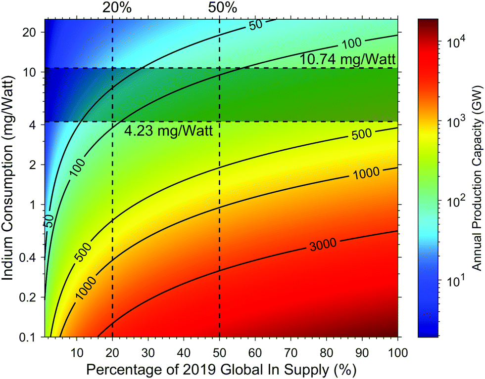 | ||
| Fig. 11 The allowable annual production capacity as a function of the percentage of 2019 global Indium supply and the Indium consumption (mg W−1) per cell in typical SHJ solar cells. The assumed cell efficiency is 25.11% with an area of 210 × 210 mm2. Shaded regions represent the range of indium consumption in current SHJ solar cells shown in Table 7. | ||
Such an aggressive reduction in the thickness of ITO layers is highly unlikely to be either realistic or appropriate from the device fabrication perspective. Concerns and challenges associated with this will be discussed in detail in the next section. On the other hand, with a reduced thickness of around 30 nm for ITO layers, which may be practical and feasible in stacked TCO layer arrangements, the resource sustainable manufacturing capacity of SHJ solar cells will be substantially increased to 115–330 GW. However, this will only account for around 5–10% of a 3 TW market size, suggesting the SHJ solar cell using ITO in some form will remain a niche product.
Prospects for reduction in indium consumption
The severe limitations on the allowed thickness of ITO layers for sustainable PV manufacturing at the terawatt scale would greatly impact the ability of ITO layers to act as lateral transport and anti-reflection coating layers. Since the sheet resistance of ITO layers is inversely proportional to the thickness, the corresponding resistivity of ITO layers must be reduced by over 33–83 times so that the same lateral conductivity of 100 nm-thick ITO layers can be maintained with a thickness of 1.2–3 nm. The material conductivity of ITO layers can be improved by increasing the carrier density.101 However, this will adversely affect optical properties through increased parasitic absorption of infrared (IR) light.102 Alternatively, indium oxide layers doped with tungsten (IWO),103 cerium (ICO),104 or hydrogen (IO:H)104,105 could be used for improved sheet resistance of those layers compared with conventional ITO layers, and in some cases, where a reduced parasitic absorption of IR light is also observed due to the improved carrier mobility, leading to improvements in the IR light management and increases in short-circuit current density. However, none of these is currently known to provide a sufficiently low resistivity that can support the use of the layer below 3 nm. In addition, the extremely thin thicknesses required below 10 nm is likely to be challenging for scalable production and may also show a likelihood of forming ITO layers as isolated islands or becoming amorphous, leading to remarkable deterioration in the electric properties106–108 of ITO layers. Moreover, reducing the thickness of ITO layers could also lead to significant increases in the contact resistivity due to changes in current pathways and current crowding effect. As such, this essentially rules out the use of a single ITO or other doped indium oxide layers as a TCO for solar cells. Even tandem devices with a relaxation of series resistance due to the low Jmp/Vmp ratio by a factor of 6 compared to conventional SHJ solar cell, the value is likely still too high to allow the use of indium-based TCOs in tandem solar cells. The severe restrictions in ITO thickness due to lateral conductivity also rule out the option of using any indium-free dielectric layers in a stacked configuration together with an indium-containing ITO layer. However, the use of stacked layers with, for example, 20 nm of ITO capped by a non-indium-based TCO would greatly increase the sustainable manufacturing capacity compared to the present implementation for SHJ solar cells relying solely on ITO.Similarly, for anti-reflection purposes, one possible approach to increase the sustainable manufacturing capacity would be using multi-layered anti-reflection coatings such as a-SiOx, SiNx, MgF2 on top of extremely thin ITO layers.109–111 As a result, the overall optical reflection can be potentially minimized by adjusting the thickness or refractive index of additional anti-reflection coating layers for any given thickness of ITO layers. However, such layers would either need to be conductive to allow effective electrical contact between the chosen anti-reflection coating and the metallization scheme or patterned to enable contact between the ITO layer and metallization scheme. However, any additional layers and processes can increase the cost and complexity for the cell fabrication process.
The fabrication of back-contact SHJ solar cells could also approximately halve the indium consumption by only requiring ITO on one surface. Such structures are responsible for the highest efficiency of 26.7% reported for a silicon solar cell to date.56 Similarly, the development of TCO-free SHJ solar cell structures is being explored utilizing the bulk conductivity of silicon wafers. A recent study by Li et al. achieved an efficiency of 22.3% whereby no TCO was used on the front surface, and a SiNx layer was used as an anti-reflection coating.112 However, again, these approaches, if still requiring ITO for one surface, fall well short of that required for sustainable terawatt-scale manufacturing of SHJ solar cells.
To enable sustainable manufacturing of SHJ solar cells and futuristic tandem devices at the terawatt scale, the use of indium-free TCO layers must be explored to completely overcome limitations imposed by the indium supply. Aluminium-doped zinc oxide (AZO), as one of the very few potential candidates, has attracted significant attention due to its low-cost and abundant nature in material and capability of achieving comparable efficiencies to ITO-based SHJ solar cells. Promising efficiency results comparable to SHJ solar cells with traditional ITO layers have been reported by several authors, with efficiencies up to ∼24% reported.113–117 However, a significant amount of effort still needs to be put into battle with the relatively poor conductivity and long-term stability of AZO layers.118–120 Research on tandem devices must also focus on using indium-free TCO layers such as AZO. Without widespread adoption of indium-free TCO layers, SHJ and future tandem technology will only be suitable for niche applications.
Bismuth consumption in PV industry
In the crystalline silicon solar cell industry, Bismuth-based alloys provide a promising low-temperature alternative to the conventional Sn/Pb solders. The lead-free nature of Bi-based solders presents a more environmentally friendly option to the PV industry, which has long been criticized for the use of ribbon coating and soldering pastes containing lead, against the industry's credentials of providing clean, green energy. In addition, Bi-based alloys can be soldered at a much lower temperature, typically below 150 °C, comparing to the soldering temperature above 200 °C needed for the conventional Sn/Pb solders.121 The low-temperature Bi-based alloys could help to avoid cell breakage, cell bowing, and the formation of microcracks by reducing the thermal-induced stress caused by the mismatch of the thermal expansion coefficients of Cu ribbon wires and Si substrate, especially in solar cells fabricated on thinner and larger silicon wafers, a trend that is likely to continue in the future.10 In addition, low-temperature soldering is particularly beneficial for SHJ solar cells, of which the surface passivation quality of amorphous silicon layers could be jeopardized by any high-temperature thermal processing.58,122 The use of low-temperature alloys will likely also be important for future tandem solar cell technologies involving perovskites, again with temperature restrictions.The Bi-based low-temperature interconnection methods such as the busbar-less SmartWire technology and the MBB approach in conjunction with bismuth-coated wires/ribbons for SHJ solar cells will potentially become the standard technology of SHJ modules, which can also help to reduce the silver consumption with narrower fingers and reduced laydown For such applications, a thin coating of SnBi in the range of 3–5 μm thick may cover the copper wires.121 It is noted here that the MBB technology can also be used for PERC and TOPCon solar cells without requiring bismuth due to the relaxed thermal constraints for soldering. In terms of silver consumption, due to the absence of silver busbars and tabbing regions, the busbar-less SmartWire technology would be preferred for SHJ solar cells over the MBB technology in terms of silver consumption as it is currently used requiring busbars and tabbing regions.
While bismuth has many benefits and advantages, especially for SHJ with severe thermal constraints, the sustainability of bismuth consumption at the TW scale may be difficult to achieve or maintain. Given that the annual production of bismuth (21000 tonnes per year) is smaller than that of silver (28000 tonnes per year), it is likely that the bismuth consumption per cell must be smaller than that of silver. The allowed annual production capacity of solar cells using Bi-based interconnection wires for different Bi consumption levels can be found in Fig. 12. For the current busbar-less SmartWire configuration, with 24 wires and a typical wire diameter of 300 μm, each solar cell (210 × 210 mm2) would consume approximately 144 mg of Bi, corresponding to a bismuth consumption of 13.0 mg W−1 with 25.11% cell efficiency. This architecture is equivalent to using more than 60% of the global Bi supply in 2019 to produce ∼1 TW of solar cells. When limited to using 20% of global supply. On the other hand, when MBB schemes are used with low-temperature Bi-based wire coatings, ∼40% lower bismuth consumption can be expected for the 12BB configuration assuming a ribbon diameter of 350 μm and coating layer thickness of 5 μm. This will allow a maximum annual production capacity of 560 GW, still well short of a TW target. The limited increase in efficiency for tandem solar cells at 30% compared to 25% for SHJ solar cells falls well short of that required to enable a sustainable bismuth consumption with the current number of wires, wire diameter, and SnBi coating thickness. For example, 1 TW production of 30% efficient tandem modules with 24 wires would still consume 51% of the global bismuth supply.
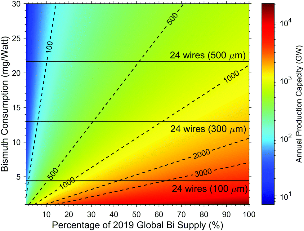 | ||
| Fig. 12 The allowable annual production capacity as a function of the percentage of global Bi supply based on 2019 and the bismuth consumption per cell. The wafer size is assumed to be 210 × 210 mm2. | ||
For a multi-TW market (e.g., 3 TW), bismuth consumption must be reduced to less than 3.5 mg W−1 if 50% of the global bismuth supply were available to the PV industry. In a more realistic but restricted scenario where 20–25% of the bismuth supply being used in PV, a bismuth consumption of no more than 1.4–1.75 mg W−1 is required. Fig. 13 shows the calculated Bismuth consumption per cell in mg W−1 as a function of the number of wires and the wire diameter, assuming each wire is coated with 3 μm thick layer of SnBi (58% Bi in weight). For 300 μm diameter wires, to have a consumption of less than 1.4 mg W−1, only 2–3 wires can be used per side, in contrast to the standard of 24 wires for SmartWire approach and 12 ribbons for MBB approach as is currently used.
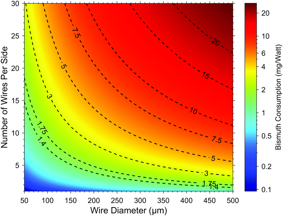 | ||
| Fig. 13 Calculated bismuth consumption as a function of the number of wires per side and the wire diameter assuming a 3 μm coating of SnBi and cell efficiency of 25.11%. | ||
Prospects for reduction in bismuth consumption
Reducing the number of wires, although reducing bismuth consumption, will significantly increase the resistive loss along fingers and along wires, which may defeat the advantage of the consumption of the SmartWire and MBB technologies using bismuth over conventional interconnection technologies. For instance, finger resistance losses will be increased by over 16–36 times compared to the current industrial 12BB configuration if only 2–3 wires can be used per side. This will likely not be feasible for any single-junction technology, including PERC, TOPCon, and SHJ solar cells. As such, the use of SmartWire or MBB interconnection with SnBi coatings as a method to reduce Ag consumption in screen-printed SHJ solar cells will also face challenges for sustainable manufacturing at the TW level.Bi-based interconnection technologies for SHJ solar cells must substantially reduce bismuth consumption. One option is to use tin-bismuth coatings with substantially lower bismuth contents, although this will increase the melting temperature of the allow. Alternative abundant low-temperature solder alloys must also be investigated. The use of electrically conductive adhesives should also be considered, which have been used for the interconnection of shingled solar cells,88,91 provided that such adhesives do not contain silver or other scarce elements.
For bismuth, tandem devices again have a unique opportunity to greatly reduce consumption through inherently lower resistive losses. For example, with a finger silver consumption of 5 mg W−1, by reducing the number of wires per side from 24 to 12 on a 210 mm cell, the sustainable manufacturing capacity of 29.1% efficiency tandem solar cells effectively doubled from 325 GW to 650 GW. Meanwhile, although the finger resistance losses will be increased by a factor of 4, finger resistance losses of such a tandem solar cell (0.41%rel) will still be lower than a SHJ solar cell with 24 wires per side.
Conclusion and future outlook
As one of the key renewable energy resources in the future global energy supply, sustainable manufacturing of solar PV will become a growing concern as the industry rapidly heading towards a multi-TW scale. Copper, steel, and aluminium are of no significant supply risks given their abundant nature and large global production scale. In addition, continued efficiency increases in solar panels will substantially reduce the consumption of these materials in terms of mg W−1 over time. However, some technology has higher material intensity comparing to the efficiency gain such that the advantage of the higher efficiency may not compensate the higher material consumption.The primary concern in heading towards sustainable PV manufacturing at the TW scale comes from silver due to its widespread use in all major industrial solar cell technologies and that it contributes a significant fraction of the non-wafer fabrication cost of the solar cell. To enable a 3 TW market, the silver consumption level must be reduced to less than 2 mg W−1. The current consumption of silver for industrial PERC solar cells is approximately 15.4 mg W−1, while that for TOPCon and SHJ solar cells are approximately double at 25.6 mg W−1 and 33.9 mg W−1, respectively, due to the reliance of silver on both the front and rear contacts. This would result in respective silver-limited sustainable manufacturing capacities of 380 GW, 230 GW, and 170 GW, given 20% of the 2019 global silver supply. Although ITRPV projections expect a 50–60% reduction in silver usage over the coming decade for each of these mainstream technologies, the expected values in 2031 are 8.5 mg W−1, 13.8 mg W−1 and 14.3 mg W−1, respectively, still well above the 2 mg W−1 target. For PERC, the expected sustainable manufacturing capacity in 2031 would be 680 GW, approximately double that of TOPCon and SHJ solar cells. This again highlights that as long as industrial TOPCon and SHJ solar cells rely on silver-screen printed contacts on both the front and rear of the solar cells, in alignment with the projections in the ITRPV, the limited efficiency gains of TOPCon and SHJ solar cells over PERC do not justify a transition away from PERC.
With industrial screen-printing technology, as it is done today, achieving the long-term target of 2 mg W−1 will be challenging. Firstly, the typical 12 busbars and soldering pad configuration already has a silver consumption of more than 4 mg W−1, which rules out the option of using existing interconnection schemes such as the MBB technology. As such, the development and deployment of new interconnection technologies with significantly reduced or zero silver consumption, such as Al/Cu busbars or busbar-less technologies, are urgently required. Replacing silver metallization schemes with aluminium or copper will not cause any supply issues for those materials, given that the consumption at the cell level is negligible compared to the existing usage in balance of systems components. Secondly, the current finger design will also face challenges from increased finger resistance power losses and a much smaller allowable cross-sectional area as the finger silver consumption is reduced. Therefore, exploring alternative materials or novel metallization designs will also be of great importance for screen printing technology. Despite a significant deviation from current industrial mainstream metallization approaches based on screen printing, solar cell technologies incorporating copper plating must also be strongly considered as a pathway to reduce silver consumption. Copper plating technology compatible with sustainable TW-scale manufacturing is already available and has been successfully deployed for large-scale production by numerous companies.
Emerging module and interconnection technologies can not only enhance the power output on the module level, but also present additional challenges and opportunities in silver reductions on the cell level. For instance, with shingled module design, the omission of the traditional soldering process eliminates the need of soldering tabs, and could also result in reduced silver consumption in busbar regions. However, the use of any silver-based ECAs may raise a new concern and needs to be carefully evaluated. One drawback of shingled cell is the significantly increased finger length, leading to a higher finger series resistance loss and imposing addition challenges to the reduction of finger silver consumption.
Indium does not pose a challenge for the mainstream PERC or emerging TOPCon solar cell technologies. Indium only poses a potential challenge for the PV industry if it deploys technologies requiring TCO layers, such as SHJ solar cells and futuristic tandem devices. Current SHJ solar cells with 200 nm of ITO (100 nm on both surfaces) consume approximately 10.7 mg W−1 of indium. This provides an extremely small sustainable manufacturing capacity of less than 40 GW. To enable a 3 TW market of solar cells using indium, the consumption must be reduced to 0.38 mg W−1. This would equate to no more than 3 nm-thick of ITO layers that can be tolerated for a 30% efficient tandem solar cell. As such, the accelerated development and deployment of indium-free TCO layers is critical for current SHJ solar cells as well as to replace interlayers in future tandem devices. Essentially no solar PV technology requiring indium can be manufactured at scale sustainably.
Similarly, bismuth does not currently pose a challenge for existing PERC or TOPCon technologies. However, the benefit of reduced soldering temperature of Bi-based solders is not only attractive for SHJ solar cells, but also for PERC and TOPCon technologies as a possible replacement for lead-based solders. In addition, the reduced soldering temperature also has the advantage of minimized damage from the thermal mismatch between ribbons and busbars, particularly beneficial for solar cells with larger and thinner silicon wafers. As a result, the use of Bi-based solders could be potentially expanded to all of PERC, TOPCon, and SHJ solar cells in the future. With a typical SmartWire configuration (24 wires on 210 × 210 mm2 cells, 300 μm diameter, and 3 μm thick coating layers), 20% of 2019 global bismuth supply can support less than 300 GW of production with such technologies. As such, Bi-based interconnection technologies must substantially reduce bismuth consumption and investigate the possibility of using more abundant low-temperature solder alloys. For example, investigating the use of tin-bismuth coatings with substantially lower bismuth contents, or alternatively the use of electrically conductive adhesives, which have been used for the interconnection of shingled solar cells.88,91
Collectively, while the current implementations of industrial TOPCon and SHJ solar cells do not create an opportunity for substantially increased sustainable manufacturing capacity over PERC, two-terminal tandem devices are exciting high-efficiency solar cell structures, which feature a unique opportunity to provide improved sustainability over the current dominant PERC solar cell technology. Firstly, there are natural benefits of significantly higher solar cell efficiencies in the vicinity of 30%. Secondly, and more importantly, owing to the property of low current density output and high voltage output through spectrum splitting, power losses contributed from series resistance components tend to be intrinsically lower in tandem structure, by a factor of 5–6 compared to that of PERC. This feature enables a unique opportunity for tandem devices to reduce the consumption of silver and bismuth simultaneously without introducing excessive resistive losses.
Author contributions
Y. Z. and M. K. performed formal analysis, visualization and wrote the manuscript. L. W. contributed to the analysis and discussion on content related to shingle and tandem solar cells, and reviewing of the manuscript. P. V. and B. H. contributed to the discussion, conceptualization, methodology, as well as reviewing and editing of the manuscript. B. H. also supervised this work.Conflicts of interest
There are no conflicts to declare.Acknowledgements
The authors would like to acknowledge Sophie Burrage who assisted with data collection and the discussion. The program has been supported by the Australian Government through the Australian Renewable Energy Agency (ARENA) and Australian Center for Advanced Photovoltaics (ACAP). The views expressed herein are not necessarily the views of the Australian Government, and the Australian Government does not accept responsibility for any information or advice contained herein. The authors would also like to thank the reviewers for their valuable comments throughout the review process.References
- United States Environmental Protection Agency, Global Greenhouse Gas Emission Data, https://www.epa.gov/ghgemissions/global-greenhouse-gas-emissions-data, (accessed 3 February 2021).
- International Energy Agency, Reneable Energy Targets by Countries, https://www.iea.org/countries, (accessed 2 February 2021).
- Clean Energy Council, Clean Energy Australia Report 2021, https://www.cleanenergycouncil.org.au/resources/resources-hub/clean-energy-australia-report, (accessed 15 May 2021).
- Institute for Energy Economics and Financial Analysis, India Ups Renewable Energy Target to 500 GW by 2030, https://ieefa.org/india-ups-renewable-energy-target-to-500gw-by-2030/, (accessed 2 February 2021).
- X. J. Yang, H. Hu, T. Tan and J. Li, Environ. Dev., 2016, 20, 83–90 CrossRef.
- The National Aeronautics and Space Administration, Climate and Earth's Energy Budget, https://earthobservatory.nasa.gov/features/EnergyBalance, (accessed 2 February 2021).
- M. A. Green, Prog. Photovoltaics, 2009, 17, 183–189 CAS.
- F. Fertig, R. Lantzsch, A. Mohr, M. Schaper, M. Bartzsch, D. Wissen, F. Kersten, A. Mette, S. Peters, A. Eidner, J. Cieslak, K. Duncker, M. Junghänel, E. Jarzembowski, M. Kauert, B. Faulwetter-Quandt, D. Meißner, B. Reiche, S. Geißler, S. Hörnlein, C. Klenke, L. Niebergall, A. Schönmann, A. Weihrauch, F. Stenzel, A. Hofmann, T. Rudolph, A. Schwabedissen, M. Gundermann, M. Fischer, J. W. Müller and D. J. W. Jeong, Energy Procedia, 2017, 124, 338–345 CrossRef CAS.
- R. Chen, H. Tong, H. Zhu, C. Ding, H. Li, D. Chen, B. Hallam, C. M. Chong, S. Wenham and A. Ciesla, Prog. Photovoltaics, 2020, 28, 1239–1247 CAS.
- ITRPV, International Technology Roadmap for Photovoltaic (ITRPV), 2020 Results, 2021.
- M. A. Green, E. D. Dunlop, J. Hohl-Ebinger, M. Yoshita, N. Kopidakis, X. Hao, J. Hohl-Ebinger, M. Yoshita, N. Kopidakis and X. Hao, Prog. Photovoltaics, 2020, 28, 629–638 Search PubMed.
- Oxford PV, Oxford PV hits new world record for solar cell, https://www.oxfordpv.com/news/oxford-pv-hits-new-world-record-solar-cell, (accessed 17 March 2021).
- M. A. Green, Joule, 2019, 3, 631–633 CrossRef.
- LAZARD, Levelized Cost of Energy Analysis - Version 13.0, 2019.
- International Energy Agency, World gross electricity production, by source, 2018, 2020.
- United Nations Climate Change, The Paris Agreement, https://unfccc.int/process-and-meetings/the-paris-agreement/the-paris-agreement, (accessed 2 February 2021).
- N. M. Haegel, H. Atwater, T. Barnes, C. Breyer, A. Burrell, Y.-M. Chiang, S. De Wolf, B. Dimmler, D. Feldman, S. Glunz, J. C. Goldschmidt, D. Hochschild, R. Inzunza, I. Kaizuka, B. Kroposki, S. Kurtz, S. Leu, R. Margolis, K. Matsubara, A. Metz, W. K. Metzger, M. Morjaria, S. Niki, S. Nowak, I. M. Peters, S. Philipps, T. Reindl, A. Richter, D. Rose, K. Sakurai, R. Schlatmann, M. Shikano, W. Sinke, R. Sinton, B. J. Stanbery, M. Topic, W. Tumas, Y. Ueda, J. van de Lagemaat, P. Verlinden, M. Vetter, E. Warren, M. Werner, M. Yamaguchi and A. W. Bett, Science, 2019, 364, 836–838 CrossRef CAS PubMed.
- P. J. Verlinden, J. Renewable Sustainable Energy, 2020, 12, 053505 CrossRef.
- C. Breyer, D. Bogdanov, A. Gulagi, A. Aghahosseini, L. S. N. S. Barbosa, O. Koskinen, M. Barasa, U. Caldera, S. Afanasyeva, M. Child, J. Farfan and P. Vainikka, Prog. Photovoltaics, 2017, 25, 727–745 Search PubMed.
- International Energy Agency, The Role of Critical Minerals in Clean Energy Transitions, 2021.
- United States Geological Survey, Copper Statistics and Information, 2020.
- E. Gervais, S. Shammugam, L. Friedrich and T. Schlegl, Renewable Sustainable Energy Rev., 2021, 137, 110589 CrossRef CAS.
- United States Geological Survey, Aluminum Statistics and Information, 2020.
- National Renewable Energy Laboratory, Expanding the Photovoltaic Supply Chain in the United States: Opportunities and Challenges, 2019.
- Worldsteel Association, World Steel in Figures (2019), 2019.
- CRC Handbook of Chemistry and Physics, ed. W. M. Haynes, CRC Press, 95th edn, 2014 Search PubMed.
- The Silver Institute, World Silver Survey 2019, 2020.
- N. Singh, H. Duan, F. Yin, Q. Song and J. Li, ACS Sustainable Chem. Eng., 2018, 6, 13016–13024 CrossRef CAS.
- CRU International, The Role of Silver in the Green Revolution, 2018.
- The Silver Institute, Market Trend Report - Silver's Growing Role in the Automotive Industry, 2021.
- National Renewable Energy Laboratory, The Availability of Indium: The Present, Medium Term, and Long Term, 2015.
- European Commission, Critical raw materials, https://ec.europa.eu/growth/sectors/raw-materials/specific-interest/critical_en, (accessed 5 March 2021).
- United States Geological Survey, Indium Statistics and Information, 2020.
- Statista, Forecast number of mobile devices worldwide from 2020 to 2024, https://www.statista.com/statistics/245501/multiple-mobile-device-ownership-worldwide/, (accessed 2 April 2021).
- Statista, Number of TV households worldwide from 2010 to 2019, https://www.statista.com/statistics/268695/number-of-tv-households-worldwide/, (accessed 2 April 2021).
- United States Geological Survey, Bismuth Statistics and Information, 2020.
- Royal Society of Chemistry, Bismuth, https://www.rsc.org/periodic-table/element/83/bismuth, (accessed 15 March 2021).
- Global Energy Monior, Datang Tuoketuo Power Station, https://www.gem.wiki/Datang_Tuoketuo_power_station, (accessed 3 August 2021).
- The Silver Institute, Silver Supply & Demand, https://www.silverinstitute.org/silver-supply-demand/, (accessed 3 August 2021).
- Trina Solar, Trina Solar Announces 23.39% PERC Solar Cell Made with Standard Fabrication Equipment, https://www.trinasolar.com/au/resources/newsroom/matrina-solar-announces-2339-perc-solar-cell-made-standard-fabrication-equipment, (accessed 3 April 2021).
- Jinko Solar, JinkoSolar Breaks World Record for P-type Monocrystalline Cell Efficiency, https://jinkosolar.eu/en/company/news-updates/reader/jinkosolar-breaks-world-record-for-p-type-monocrystalline-cell-efficiency.html, (accessed 2 April 2021).
- LONGi Solar, LONGi Solar sets new bifacial mono-PERC solar cell world record at 24.06%, https://en.longi-solar.com/home/events/press_detail/id/89.html, (accessed 27 November 2020).
- J. L. Murray and A. J. McAlister, Bull. Alloy Phase Diagrams, 1984, 5, 74–84 CrossRef CAS.
- S. Fritz, M. Konig, S. Riegel, A. Herguth, M. Horteis and G. Hahn, IEEE J. Photovoltaics, 2015, 5, 145–151 Search PubMed.
- J. Lindroos and H. Savin, Sol. Energy Mater. Sol. Cells, 2016, 147, 115–126 CrossRef CAS.
- P. Zhu, Y. Liu, C. Cao, J. Tian, A. Zhang and D. Wang, Materials, 2021, 14, 765 CrossRef CAS PubMed.
- D. Wood, I. Kuzma-Filipek, R. Russell, F. Duerinckx, N. Powell, A. Zambova, B. Chislea, P. Chevalier, C. Boulord, A. Beucher, N. Zeghers, W. W. Deng, Z. Feng, P. Verlinden, J. Szlufcik and G. Beaucarne, Energy Procedia, 2014, 55, 724–732 CrossRef CAS.
- S. Rommel, F. Einsele, H. Guo, M. F. Ametowobla and D. Manz, Proc. 26th Eur. Photovolt. Sol. Energy Conf. Exhib., 2011, 1538–1541.
- P. Papet, R. Efinger, B. Sadlik, Y. Andrwult, D. Batzner, D. Lachernal, B. Strahm, G. Wahli, F. Wuensch, W. Frammelsberger, W. Stein, L. Rubin, W. Schmutz, A. Buechel and B. Ran, 26th European Photovoltaic Solar Energy Conference and Exhibition, Hamburg, 2011, pp. 3336–3339.
- TaiyangNews, Market Survey – Metallization Pastes 2019/2020, 2020.
- T. G. Allen, J. Bullock, X. Yang, A. Javey and S. De Wolf, Nat. Energy, 2019, 4, 914–928 CrossRef CAS.
- F. Haase, C. Hollemann, S. Schäfer, A. Merkle, M. Rienäcker, J. Krügener, R. Brendel and R. Peibst, Sol. Energy Mater. Sol. Cells, 2018, 186, 184–193 CrossRef CAS.
- A. Richter, R. Müller, J. Benick, F. Feldmann, B. Steinhauser, C. Reichel, A. Fell, M. Bivour, M. Hermle and S. W. Glunz, Nat. Energy, 2021, 6, 429–438 CrossRef CAS.
- A. Richter, J. Benick, F. Feldmann, A. Fell, B. Steinhauser, J.-I. Polzin, N. Tucher, J. N. Murthy, M. Hermle and S. W. Glunz, 36th Eur. PV Sol. Energy Conf. Exhib., 2019, 9–13.
- Jinko Solar, JinkoSolar Large-Area N-Type Monocrystalline Silicon Solar Cell Reaches Record-breaking New High Efficiency of 25.25%, https://www.jinkosolar.com/en/site/newsdetail/1553, (accessed 2 June 2021).
- K. Yoshikawa, W. Yoshida, T. Irie, H. Kawasaki, K. Konishi, H. Ishibashi, T. Asatani, D. Adachi, M. Kanematsu, H. Uzu and K. Yamamoto, Sol. Energy Mater. Sol. Cells, 2017, 173, 37–42 CrossRef CAS.
- LONGi Solar, LONGi breaks three more world records for solar cell efficiency, https://en.longi-solar.com/home/events/press_detail/id/335.html, (accessed 2 June 2021).
- S. DeWolf, A. Descoeudres, Z. C. Holman, C. Ballif, S. De Wolf, A. Descoeudres, Z. C. Holman and C. Ballif, Green, 2012, 2, 7–24 CrossRef CAS.
- TaiyangNews, Heterojunction Solar Technology - 2019 Edition, 2019.
- T. Tiedje, E. Yablonovitch, G. D. Cody and B. G. Brooks, IEEE Trans. Electron Devices, 1984, 31, 711–716 Search PubMed.
- K. Yoshikawa, H. Kawasaki, W. Yoshida, T. Irie, K. Konishi, K. Nakano, T. Uto, D. Adachi, M. Kanematsu, H. Uzu and K. Yamamoto, Nat. Energy, 2017, 2, 17032 CrossRef CAS.
- T. Leijtens, K. A. Bush, R. Prasanna and M. D. McGehee, Nat. Energy, 2018, 3, 828–838 CrossRef CAS.
- J. F. Geisz, R. M. France, K. L. Schulte, M. A. Steiner, A. G. Norman, H. L. Guthrey, M. R. Young, T. Song and T. Moriarty, Nat. Energy, 2020, 5, 326–335 CrossRef CAS.
- Oxford PV, Oxford PV continues to prepare for volume manufacturing, https://www.oxfordpv.com/news/oxford-pv-continues-prepare-volume-manufacturing, (accessed 2 August 2021).
- Oxford PV, Oxford PV completes build-out of its Brandenburg factory, https://www.oxfordpv.com/news/oxford-pv-completes-build-out-its-brandenburg-factory, (accessed 2 August 2021).
- A. Faes, L. Curvat, H. Li, J. Levrat, J. Champliaud, K. Thomas, J. Escarré, N. Badel, B. Paviet-Salomon, J. Geissbühler, C. Allebé, L. Barraud, F. Debrot, A. Descoeudres, A. Lachowicz, J. Horzel, L. Lou Senaud, L. E. Perret-Aebi, C. Ballif and M. Despeisse, 2018 IEEE 7th World Conf. Photovolt. Energy Conversion, WCPEC 2018 - A Jt. Conf. 45th IEEE PVSC, 28th PVSEC 34th EU PVSEC, 2018, 1998–2001.
- S. Tepner, N. Wengenmeyr, M. Linse, A. Lorenz, M. Pospischil and F. Clement, Adv. Mater. Technol., 2020, 5, 1–9 Search PubMed.
- Y. Chen, Y. Yang, W. Deng, A. Ali, P. J. Verlinden and P. P. Altermatt, Energy Procedia, 2016, 98, 30–39 CrossRef CAS.
- S. Braun, G. Micard and G. Hahn, Energy Procedia, 2012, 27, 227–233 CrossRef.
- S. Tepner, L. Ney, M. Linse, A. Lorenz, M. Pospischil, K. Masuri and F. Clement, Prog. Photovoltaics, 2020, 28, 1054–1062 CAS.
- M. Yamaguchi, K.-H. Lee, K. Araki and N. Kojima, J. Phys. D. Appl. Phys., 2018, 51, 133002 CrossRef.
- F. Meillaud, A. Shah, C. Droz, E. Vallat-Sauvain and C. Miazza, Sol. Energy Mater. Sol. Cells, 2006, 90, 2952–2959 CrossRef CAS.
- A. Al-Ashouri, E. Köhnen, B. Li, A. Magomedov, H. Hempel, P. Caprioglio, J. A. Márquez, A. B. Morales Vilches, E. Kasparavicius, J. A. Smith, N. Phung, D. Menzel, M. Grischek, L. Kegelmann, D. Skroblin, C. Gollwitzer, T. Malinauskas, M. Jošt, G. Matič, B. Rech, R. Schlatmann, M. Topič, L. Korte, A. Abate, B. Stannowski, D. Neher, M. Stolterfoht, T. Unold, V. Getautis and S. Albrecht, Science, 2020, 370, 1300–1309 CrossRef CAS PubMed.
- A. Lennon, J. Colwell and K. P. Rodbell, Prog. Photovoltaics, 2019, 27, 67–97 CAS.
- T. Bmton, N. Mason, S. Roberts, O. N. Hartley, S. Gledhill, J. Femandez, R. Russell, W. Warta, S. Glunz, O. Schultz, M. Hermle and G. Willeke, 3rd World Conference on Photovoltaic Energy Conversion, 2003, vol. 1, pp. 899–902.
- S. R. Wenham, C. B. Honsberg and M. A. Green, Sol. Energy Mater. Sol. Cells, 1994, 34, 101–110 CrossRef CAS.
- N. Nampalli, D. Jordan, A. Lennon, R. Evans, S. Wenham and M. Edwards, 6th World Conf. Photovolt. Energy Convers., 2014, 1091–1092.
- Z. Wang, P. Han, H. Lu, H. Qian, L. Chen, Q. Meng, N. Tang, F. Gao, Y. Jiang, J. Wu, W. Wu, H. Zhu, J. Ji, Z. Shi, A. Sugianto, L. Mai, B. Hallam and S. Wenham, Prog. Photovoltaics, 2012, 20, 260–268 CAS.
- Z. Shi, S. Wenham and J. Ji, 2009 34th IEEE Photovoltaic Specialists Conference (PVSC), IEEE, 2009, pp. 001922–001926.
- M. Osborne, Meco's ‘Cell Plating Line’ enables lower cost high-efficiency solar cells, https://www.pv-tech.org/mecos-cell-plating-line-enables-lower-cost-high-efficiency-solar-cells/, (accessed 23 May 2021).
- O. Schultz-wittmann, A. Turner, B. Eggleston, D. De Ceuster, D. Suwito, E. Van, S. Baker-finch and V. Prajapati, Proc. 32nd Eur. Photovolt. Sol. Energy Conf., 2016, M, 456–459.
- W. P. Mulligan, M. J. Cudzinovic, T. Pass, D. Smith and R. M. Swanson, US20040200520A1, 2003.
- D.-H. Neuhaus and A. Münzer, Adv. OptoElectron., 2007, 2007, 1–15 CrossRef.
- V. Arya, B. Steinhauser, B. Gruebel, C. Schmiga, N. Bay, D. Brunner, M. Passig, A. A. Brand, S. Kluska and J. Nekarda, Phys. Status Solidi Appl. Mater. Sci., 2020, 217, 1–9 Search PubMed.
- G. Cimiotti, J. Bartsch, A. Kraft, A. Mondon and M. Glatthaar, Energy Procedia, 2015, 67, 84–92 CrossRef CAS.
- F. Feldmann, B. Steinhauser, T. Pernau, H. Nagel, T. Fellmeth, S. Mack, D. Ourinson, E. Lohmüller, J. I. Polzin, A. Moldovan, M. Bivour, F. Clement, J. Rentsch, M. Hermle and S. W. Glunz, 37th European Photovoltaic Solar Energy Conference and Exhibition, 2018, pp. 164–169.
- S. Guo, J. P. Singh, I. M. Peters, A. G. Aberle and T. M. Walsh, Int. J. Photoenergy, 2013, 2013, 1–8 CrossRef.
- L. Theunissen, B. Willems, J. Burke, D. Tonini, M. Galiazzo and A. Henckens, AIP Conference Proceedings, 2018, vol. 1999, p. 080003.
- M. Mittag, T. Zech, M. Wiese, D. Blasi, M. Ebert and H. Wirth, 2017 IEEE 44th Photovoltaic Specialist Conference (PVSC), IEEE, 2017, pp. 1531–1536.
- W. Oh, J. Park, S. Dimitrijev, E. K. Kim, Y. S. Park and J. Lee, Sol. Energy, 2020, 195, 527–535 CrossRef CAS.
- G. Beaucarne, Energy Procedia, 2016, 98, 115–124 CrossRef CAS.
- A. Faes, A. Lachowicz, A. Bettinelli, P.-J. Ribeyron, D. Muñoz, J.-F. Lerat, J. Geissbühler, H.-Y. Li, C. Ballif and M. Despeisse, Photovoltaics Bull., 2018, 41, 65 Search PubMed.
- H. Zhou and L. Zhou, AU2018402719A1, 2019.
- Y. Yang, S. Feng, M. Li, W. Xu, G. Yin, Z. Wang, B. Sun and X. Gao, Sci. Rep., 2017, 7, 1–9 CrossRef PubMed.
- W. Li, J. Zheng, B. Hu, H. C. Fu, M. Hu, A. Veyssal, Y. Zhao, J. H. He, T. L. Liu, A. Ho-Baillie and S. Jin, Nat. Mater., 2020, 19, 1326–1331 CrossRef CAS PubMed.
- Z. Jia, S. Qin, L. Meng, Q. Ma, I. Angunawela, J. Zhang, X. Li, Y. He, W. Lai, N. Li, H. Ade, C. J. Brabec and Y. Li, Nat. Commun., 2021, 12, 1–10 CrossRef PubMed.
- F. Sahli, J. Werner, B. A. Kamino, M. Bräuninger, R. Monnard, B. Paviet-Salomon, L. Barraud, L. Ding, J. J. Diaz Leon, D. Sacchetto, G. Cattaneo, M. Despeisse, M. Boccard, S. Nicolay, Q. Jeangros, B. Niesen and C. Ballif, Nat. Mater., 2018, 17, 820–826 CrossRef CAS PubMed.
- Von Ardenne, Industrial TCOs for SHJ solar cells: Approaches for optimizing performance and cost, https://www.vonardenne.biz/en/company/press-events/industrial-tcos-for-shj-solar-cells/, (accessed 17 May 2021).
- F. Colville, PV CellTech Online Conference (Oral presentation), 2020 Search PubMed.
- S. K. Chunduri, SHJ workshop (Oral presentation), 2020 Search PubMed.
- S. Kirner, M. Hartig, L. Mazzarella, L. Korte, T. Frijnts, H. Scherg-Kurmes, S. Ring, B. Stannowski, B. Rech and R. Schlatmann, Energy Procedia, 2015, 77, 725–732 CrossRef CAS.
- Z. C. Holman, A. Descoeudres, L. Barraud, F. Z. Fernandez, J. P. Seif, S. De Wolf and C. Ballif, IEEE J. Photovoltaics, 2012, 2, 7–15 Search PubMed.
- L. Ding, J. D. Leon, G. Christmann and S. Nicolay, CSEM Scientific and Technical Report: Development of High Mobility TCOs for Heterojunction Solar Cells, 2018 Search PubMed.
- E. Kobayashi, Y. Watabe, T. Yamamoto and Y. Yamada, Sol. Energy Mater. Sol. Cells, 2016, 149, 75–80 CrossRef CAS.
- L. Barraud, Z. C. Holman, N. Badel, P. Reiss, A. Descoeudres, C. Battaglia, S. De Wolf and C. Ballif, Sol. Energy Mater. Sol. Cells, 2013, 115, 151–156 CrossRef CAS.
- J. Gwamuri, A. Vora, J. Mayandi, D. Güney, P. L. Bergstrom and J. M. Pearce, Sol. Energy Mater. Sol. Cells, 2016, 149, 250–257 CrossRef CAS.
- J. Gwamuri, A. Vora, R. R. Khanal, A. B. Phillips, M. J. Heben, D. O. Guney, P. Bergstrom, A. Kulkarni and J. M. Pearce, Mater. Renewable Sustainable Energy, 2015, 4, 1–11 CrossRef.
- J. W. Cleary, E. M. Smith, K. D. Leedy, G. Grzybowski and J. Guo, Opt. Mater. Express, 2018, 8, 1231 CrossRef CAS.
- M. Boccard, L. Antognini, J. Cattin, J. Dreon, O. Dupre, A. Fioretti, J. Haschke, R. Monnard, M. Morales-Masis, V. Paratte, E. Rucavado, L. Lou Senaud, S. Zhong, B. Paviet-Salomon, M. Despeisse and C. Ballif, Conf. Rec. IEEE Photovolt. Spec. Conf., 2019, 2541–2545.
- J. Yu, J. Zhou, J. Bian, J. Shi, L. Zhang, F. Meng and Z. Liu, 2018 IEEE 7th World Conf. Photovolt. Energy Conversion, WCPEC 2018 - A Jt. Conf. 45th IEEE PVSC, 28th PVSEC 34th EU PVSEC, 2018, 49–52.
- D. Zhang, I. A. Digdaya, R. Santbergen, R. A. C. M. M. Van Swaaij, P. Bronsveld, M. Zeman, J. A. M. Van Roosmalen and A. W. Weeber, Sol. Energy Mater. Sol. Cells, 2013, 117, 132–138 CrossRef CAS.
- J. Haschke, G. Christmann, C. Messmer, M. Bivour, M. Boccard and C. Ballif, J. Appl. Phys., 2020, 127, 114501 CrossRef CAS.
- A. B. Morales-Vilches, A. Cruz, S. Pingel, S. Neubert, L. Mazzarella, D. Meza, L. Korte, R. Schlatmann and B. Stannowski, IEEE J. Photovoltaics, 2019, 9, 34–39 Search PubMed.
- D. Meza, A. Cruz, A. Morales-Vilches, L. Korte and B. Stannowski, Appl. Sci., 2019, 9, 862 CrossRef CAS.
- A. Cruz, E. C. Wang, A. B. Morales-Vilches, D. Meza, S. Neubert, B. Szyszka, R. Schlatmann and B. Stannowski, Sol. Energy Mater. Sol. Cells, 2019, 195, 339–345 CrossRef.
- Z. Wu, W. Duan, A. Lambertz, D. Qiu, M. Pomaska, Z. Yao, U. Rau, L. Zhang, Z. Liu and K. Ding, Appl. Surf. Sci., 2021, 542, 148749 CrossRef CAS.
- L. Lou Senaud, G. Christmann, A. Descoeudres, J. Geissbuhler, L. Barraud, N. Badel, C. Allebe, S. Nicolay, M. Despeisse, B. Paviet-Salomon and C. Ballif, IEEE J. Photovoltaics, 2019, 9, 1217–1224 Search PubMed.
- T. Tohsophon, J. Hüpkes, S. Calnan, W. Reetz, B. Rech, W. Beyer and N. Sirikulrat, Thin Solid Films, 2006, 511–512, 673–677 CrossRef CAS.
- D. Greiner, S. E. Gledhill, C. Köble, J. Krammer and R. Klenk, Thin Solid Films, 2011, 520, 1285–1290 CrossRef CAS.
- J. Hüpkes, J. I. Owen, M. Wimmer, F. Ruske, D. Greiner, R. Klenk, U. Zastrow and J. Hotovy, Thin Solid Films, 2014, 555, 48–52 CrossRef.
- L. E. García, A. Faes, M. Despeisse, J. Levrat, J. Champliaud, N. Badel, M. Kiaee, T. Söderström, Y. Yao, R. Grischke, M. Gragert, J. Ufheil, P. Papet, B. Strahm, B. Cattaneo, J. Cattin, Y. Baumgartner, A. Hessler-Wyser and C. BallifReyes, 29th European Photovoltaic Solar Energy Conference and Exhibition, 2013, vol. 5DO.16.3, pp. 2555–2561.
- A. Descoeudres, C. Allebé, N. Badel, L. Barraud, J. Champliaud, G. Christmann, F. Debrot, A. Faes, J. Geissbühler, J. Horzel, A. Lachowicz, J. Levrat, S. Martin de Nicolas, S. Nicolay, B. Paviet-Salomon, L. L. Senaud, C. Ballif and M. Despeisse, Sol. Energy, 2018, 175, 54–59 CrossRef CAS.
- M. Müller, G. Fischer, B. Bitnar, S. Steckemetz, R. Schiepe, M. Mühlbauer, R. Köhler, P. Richter, C. Kusterer, A. Oehlke, E. Schneiderlöchner, H. Sträter, F. Wolny, M. Wagner, P. Palinginis and D. H. Neuhaus, Energy Procedia, 2017, 124, 131–137 CrossRef.
- D. Chen, Y. Chen, Z. Wang, J. Gong, C. Liu, Y. Zou, Y. He, Y. Wang, L. Yuan, W. Lin, R. Xia, L. Yin, X. Zhang, G. Xu, Y. Yang, H. Shen, Z. Feng, P. P. Altermatt and P. J. Verlinden, Sol. Energy Mater. Sol. Cells, 2020, 206, 1–8 Search PubMed.
- LONGi Solar, LONGi sets record of 25.09% for N-Type TOPCon cell efficiency, https://en.longi-solar.com/home/events/press_detail/id/331.html, (accessed 7 May 2021).
- C. Liu, D. Chen, Y. Chen, Y. Ling, Y. Zou, Y. Wang, J. Gong, Z. Feng, P. P. Altermatt and P. J. Verlinden, Sol. Energy Mater. Sol. Cells, 2020, 215, 110690 CrossRef CAS.
- X. Ru, M. Qu, J. Wang, T. Ruan, M. Yang, F. Peng, W. Long, K. Zheng, H. Yan and X. Xu, Sol. Energy Mater. Sol. Cells, 2020, 215, 110643 CrossRef CAS.
- J. Dréon, Q. Jeangros, J. Cattin, J. Haschke, L. Antognini, C. Ballif and M. Boccard, Nano Energy, 2020, 70, 104495 CrossRef.
- T. Kinoshita, D. Fujishima, A. Yano, A. Ogane, S. Tohoda, K. Matsuyama, Y. Nakamura, N. Tokuoka, H. Kanno, H. Sakata, M. Taguchi and E. Maruyama, 26th Eur. Photovolt. Sol. Energy Conf. Exhib., 2011, 871–874.
- J. Zheng, H. Mehrvarz, C. Liao, J. Bing, X. Cui, Y. Li, V. R. Goncąles, C. F. J. Lau, D. S. Lee, Y. Li, M. Zhang, J. Kim, Y. Cho, L. G. Caro, S. Tang, C. Chen, S. Huang and A. W. Y. Ho-Baillie, ACS Energy Lett., 2019, 4, 2623–2631 CrossRef CAS.
- Y. Wu, D. Yan, J. Peng, T. Duong, Y. Wan, S. P. Phang, H. Shen, N. Wu, C. Barugkin, X. Fu, S. Surve, D. Grant, D. Walter, T. P. White, K. R. Catchpole and K. J. Weber, Energy Environ. Sci., 2017, 10, 2472–2479 RSC.
- J. Xu, C. C. Boyd, Z. J. Yu, A. F. Palmstrom, D. J. Witter, B. W. Larson, R. M. France, J. Werner, S. P. Harvey, E. J. Wolf, W. Weigand, S. Manzoor, M. F. A. M. Van Hest, J. J. Berry, J. M. Luther, Z. C. Holman and M. D. McGehee, Science, 2020, 367, 1097–1104 CrossRef CAS PubMed.
- C. Messmer, B. S. Goraya, S. Nold, P. S. C. Schulze, V. Sittinger, J. Schön, J. C. Goldschmidt, M. Bivour, S. W. Glunz and M. Hermle, Prog. Photovoltaics, 2020, 1–16 Search PubMed.
- A. Louwen, W. G. J. H. M. Van Sark, R. E. I. Schropp, W. C. Turkenburg and A. P. C. Faaij, Prog. Photovoltaics, 2015, 23, 1406–1428 CAS.
- J. Haschke, O. Dupré, M. Boccard and C. Ballif, Sol. Energy Mater. Sol. Cells, 2018, 187, 140–153 CrossRef CAS.
Footnote |
| † Authors contributed equally. |
| This journal is © The Royal Society of Chemistry 2021 |