
 Open Access Article
 This Open Access Article is licensed under a
 Creative Commons Attribution 3.0 Unported Licence
Ligand-bridged charge extraction and enhanced quantum efficiency enable efficient n–i–p perovskite/silicon tandem solar cells†
Erkan
Aydin
 *a,
Jiang
Liu
a,
Esma
Ugur
a,
Randi
Azmi
a,
George T.
Harrison
a,
Yi
Hou
b,
Bin
Chen
b,
Shynggys
Zhumagali
a,
Michele
De Bastiani
a,
Mingcong
Wang
a,
Waseem
Raja
a,
Thomas G.
Allen
a,
Atteq ur
Rehman
a,
Anand S.
Subbiah
a,
Maxime
Babics
a,
Aslihan
Babayigit
ac,
Furkan H.
Isikgor
a,
Kai
Wang
a,
Emmanuel
Van Kerschaver
a,
Leonidas
Tsetseris
d,
Edward H.
Sargent
b,
Frédéric
Laquai
a and
Stefaan
De Wolf
*a
*a,
Jiang
Liu
a,
Esma
Ugur
a,
Randi
Azmi
a,
George T.
Harrison
a,
Yi
Hou
b,
Bin
Chen
b,
Shynggys
Zhumagali
a,
Michele
De Bastiani
a,
Mingcong
Wang
a,
Waseem
Raja
a,
Thomas G.
Allen
a,
Atteq ur
Rehman
a,
Anand S.
Subbiah
a,
Maxime
Babics
a,
Aslihan
Babayigit
ac,
Furkan H.
Isikgor
a,
Kai
Wang
a,
Emmanuel
Van Kerschaver
a,
Leonidas
Tsetseris
d,
Edward H.
Sargent
b,
Frédéric
Laquai
a and
Stefaan
De Wolf
*a
aKing Abdullah University of Science and Technology (KAUST), KAUST Solar Center (KSC), Physical Sciences and Engineering Division (PSE), Thuwal 23955-6900, Kingdom of Saudi Arabia. E-mail: erkan.aydin@kaust.edu.sa; stefaan.dewolf@kaust.edu.sa
bUniversity of Toronto, Department of Electrical and Computer Engineering, Toronto, Ontario M5S 1A4, Canada
cHasselt University, Institute for Materials Research (IMO), Wetenschapspark 1, 3590 Diepenbeek, Limburg, Belgium
dNational Technical University of Athens, Department of Physics, GR15780 Athens, Greece
First published on 30th June 2021
Abstract
Translating the high power conversion efficiencies of single-junction perovskite solar cells in their classic, non-inverted (n–i–p) architecture to efficient monolithic n–i–p perovskite/silicon tandem solar cells with high current densities has been a persistent challenge due to the lack of low-temperature processable, chemically-insoluble contact materials with appropriate polarity and sufficient optical transparency. To address this, we developed sputtered amorphous niobium oxide (a-NbOx) with ligand-bridged C60 as an efficient electron-selective contact, deposited on the textured-silicon bottom cell. For the sunward, hole-selective contact we implemented a stack of molecularly doped broadband transparent evaporated 2,2′,7,7′-tetra(N,N-di-p-tolyl)amino-9,9-spirobifluorene (spiro-TTB) and atomic layer deposited vanadium oxide, which further enhances the device quantum efficiency. Combining these contact materials with two-dimensional perovskite passivation on the micrometer-thick solution-processed perovskite top cell yields 27% efficient monolithic n–i–p perovskite/silicon tandem solar cells, which represents one of the highest power conversion efficiencies reported on pyramidal textured crystalline silicon bottom cells, and the highest with this polarity.
Broader contextMonolithic perovskite/silicon tandem solar cells are of interest thanks to their high power conversion efficiency potential at affordable cost. Also, the possibility to fabricate silicon heterojunction bottom cells either in the n–i–p or p–i–n polarity provides considerable flexibility to choose the device architecture. The initial perovskite/silicon tandems were in the n–i–p configuration. However, as in this architecture light enters from the p-side, the application of the typical electron and hole selective contacts of single-junction devices to the tandem configuration resulted in devices with a poor blue response, in particular due to parasitic absorption in the front-contact stack. Therefore, global tandem research refocused on the inverted structure (p–i–n configuration, with electron collection at the front), and so far, several efficient devices have been reported in this configuration. Increasingly the power conversion efficiency of p–i–n tandems further is constrained by parasitic absorption and recombination active defects in the front SnOx/C60 electron selective layer stack, prompting us to revisit the n–i–p structure with the aim to benefit from the wide library of efficient hole selective layers in single-junction n–i–p perovskite solar cells. In this work, we systematically overcome the persistent challenges of n–i–p tandem devices by developing novel electron and hole selective contact stacks, fully processed on industry-standard textured silicon bottom cells. Our work enables a new device platform and research avenues to further push the efficiency of perovskite-based tandem solar cells. |
Introduction
Metal halide perovskite solar cells (PSCs) have been reported with many different material combinations and device configurations. However, in silicon-based tandem architectures, most of the studies in literature have been in the p–i–n configuration.1–8 Although single-junction n–i–p devices have systematically proven higher power conversion efficiencies (PCEs),9–11 their translation to the perovskite/silicon tandem configuration has been hindered by (i) a lack of low-temperature processable, chemically insoluble, and conformal electron-selective layers (ESLs), (ii) a lack of efficient, conformal, and optically transparent hole-selective contact stacks, and (iii) an inability to fabricate the perovskite top cell on micron-sized pyramidal textured interfaces, as employed in high-efficiency silicon solar cells.12 These challenges have limited the performance of n–i–p tandems to ∼22% (>1 cm2) on silicon heterojunction (SHJ) cells, and ∼24% (1 cm2) on poly-silicon passivating-contact silicon solar cells,13 even though all initial perovskite/silicon tandems were in the n–i–p configuration.14–17In the single-junction n–i–p configuration, several well-established ESLs are available, such as the archetypal compact and mesoporous titanium dioxide (c-TiO2/m-TiO2) stack, which requires a high-temperature sintering step (>450 °C), however.11,18,19 This temperature requirement excludes the applicability of this ESL stack for tandems built onto high-performance SHJ bottom cells,20 whose temperature processing window is <250 °C due to their amorphous-silicon passivated surfaces. Thin films of tin oxide nanoparticles (np-SnOx) are also increasingly used as an ESL on PSCs,21 and these are usually deposited at lower temperatures (<200 °C).22,23 However, np-SnOx ESLs are solution-processed. As a result, achieving conformal deposition on rough, complex surfaces, such as pyramidal-textured silicon, is difficult. Furthermore, thermally-evaporated C60 is a successful ESL, but is soluble by subsequent perovskite solution processing.
In the search for alternative ESLs, thin-film niobium pentoxide (Nb2O5) stands out as it combines favorable properties such as a low work function (WF), a wide bandgap, high chemical and ultraviolet (UV) light stability, as well as compatibility with various processing techniques.24–28 To adopt such Nb2O5 layers to n–i–p tandems as an ESL, we employed the RF-sputtering technique. Using stoichiometric targets under an argon atmosphere, we achieved a slightly oxygen (O) deficient and amorphous film structure. Notably, we find that such O vacancies in the amorphous phase do not induce deep-level trap states, in contrast to np-SnOx, but rather act as shallow donor-like defects that improve the conductivity and mobility in the bulk of the film, and promote charge extraction through the contact structure. Modification of the charge transport layer/perovskite interface with C60 derivatives is a successful strategy to further enhance electron extraction.29–32 To apply this at a-NbOx/perovskite interface, we utilize C60 with a functionalized pyrrolidine tail to create a conformal self-assembled molecular monolayer (SAM), anchored on the a-NbOx surface, which makes it insoluble to the aprotic solvents used in perovskite solution processing. To support our findings, we theoretically underpin this self-anchoring interaction by density functional theory (DFT) calculations. On the device-level, we show high PCE values for both perovskite single-junction and perovskite/silicon tandem solar cells utilizing C60-anchored a-NbOx ESLs, thanks to reduced non-radiative recombination at the interface.
Another major factor hindering the progress of n–i–p tandems has been the lack of efficient, optically transparent, and conformal hole selective layers (HSLs) and buffer layers. Such buffer layers protect the soft perovskite absorber from sputter damage during the deposition of the top transparent conductive oxide (TCO). In the more widespread p–i–n tandem configuration, a bilayer consisting of an evaporated C60 ESL, followed by an ALD SnOx buffer layer, is employed, onto which a TCO is sputtered. So far, the most widely reported HSL for n–i–p devices is spiro-OMeTAD, but this material suffers from strong parasitic absorption in the blue part of the solar spectrum, and requires post oxidation with metal–organic complexes for improved hole mobility.33 Nevertheless, several thermally evaporable small-molecule HSLs could be used.34,35 However, the common issue with these molecules is their low hole mobility, low electrical conductivity, and unfavorable ionization potential.36 To address this, we evaporated small molecule HSLs [2,2′,7,7′-tetra(N,N-di-p-tolyl)amino-9,9-spirobifluorene (spiro-TTB)2 and N4,N4,N4′′,N4′′-tetra([1,1′-biphenyl]-4-yl)-[1,1′:4′,1′′-terphenyl]-4,4′′-diamine (TaTm)37] and doped them using the strong electron-accepting molecule 2,2′-(perfluoronaphthalene-2,6-diylidene) dimalononitrile (F6-TCNNQ)38 to enhance the hole mobility and conductivity. Finally, we tested these HSLs in bilayer stacks with vanadium oxide (VOx)39 and tungsten oxide (WOx) as buffer layers, first in single-junction devices, and then in monolithic perovskite/silicon tandems. On our optimized devices, we used doped spiro-TTB/VOx bilayers as an HSL stack.
To minimize reflection losses from the silicon bottom cells,1–3,7,8 we utilized textured SHJ bottom cells, onto which micrometer-thick perovskites were solution-processed. In addition, we utilized a mixed 2D/3D passivation treatment on the perovskite top surface for improved charge extraction, and reduced hysteresis, which have been implemented usually in n–i–p configuration devices to date. Combining minimized reflection losses with reduced parasitic absorption by evaporated HSLs enabled one of the highest PCEs for tandems on textured interfaces. Combined, these systematic improvements in the n–i–p tandem device design solve the persistent issues that have hindered their progress on SHJ bottom cells, resulting in an improvement in PCE from ∼22%17 to over 27%, a performance that is commensurate with its state-of-the-art p–i–n tandem counterparts.
Characteristics of pristine and C60-anchored a-NbOx films
Scanning electron microscope (SEM) and atomic force microscopy (AFM) top-view images reveal the amorphous morphology of our sputtered NbOx films (Fig. 1a and Fig. S1c, respectively, ESI†). Unlike spin-casted np-SnOx films (Fig. S1b, ESI†), our a-NbOx films show a high conformality on the textured-Si surface, which is critical for tandem integration (Fig. 1b). High-resolution transmission electron microscopy (HR-TEM) (Fig. 1c), and surface-sensitive grazing incidence X-ray diffraction (GIXRD) measurements of a-NbOx films (Fig. 1d) confirm the amorphous nature of the material. In addition, post-deposition annealing of the films at elevated temperature (up to 500 °C) does not lead to crystal formation, as shown by the XRD graphs in the inset figure of Fig. 1d.40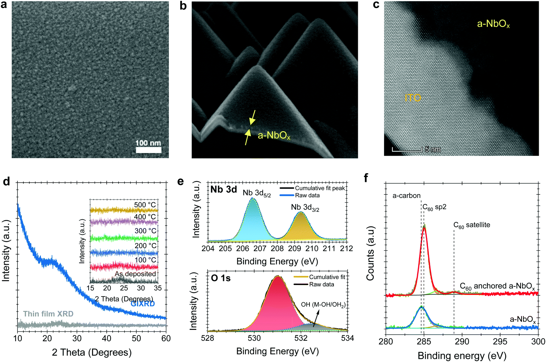 | ||
| Fig. 1 SEM images of the a-NbOx films (a) on soda-lime glass substrates and (b) on textured crystalline silicon. (c) Cross-sectional HR-TEM image of the a-NbOx films deposited on crystalline ITO. (d) XRD graph of the a-NbOx films with powder XRD and GIXRD analysis, which does not reveal any prominent peak. The inset figure in panel d shows the powder XRD of the films post-annealed at different temperatures. HR-XPS spectra of the (e) Nb 3d, and O 1s states of a-NbOx films together with (f) XPS spectra of a-NbOx and C60-anchored a-NbOx films. | ||
The multi-valent nature of niobium (Nb) leads to various stable oxidation states (+2, +4 and +5), resulting in different polymorphs such as NbO, NbO2, and Nb2O5.41 Here, our amorphous films are sputtered from a Nb2O5 target in a pure Ar atmosphere (without intentional oxygen flow), yielding nearly stoichiometric Nb2O5 films, which is thermodynamically the most stable phase.42 Nevertheless, our a-NbOx films are slightly O-deficient, according to our X-ray photoelectron spectroscopy (XPS) analysis (Note S1, ESI†). The O-deficient character of the a-NbOx films is further demonstrated by a two orders of magnitude decrease in electrical conductivity of the films after annealing in ambient air (Note S2, ESI†).40,43 We investigate the chemical structure of the a-NbOx (Fig. 1e) and np-SnOx (Fig. S2, ESI†) films using high-resolution XPS spectra, which show that Nb ions exist in single metal-oxide environments of Nb5+ with Nb 3d 5/2 (207.3 eV). The elemental composition of the films by wide survey XPS scans (Fig. S2a and b, ESI†) revealed an atomic percentage ratio of Nb/Ometaloxide = 1/2.2 and Sn/Ometaloxide = 1/1.8 for a-NbOx and np-SnOx, respectively (see Note S1, ESI† for a detailed analysis). These results indicate a slightly O-deficient nature of the films, resulting in improved conductivity. We confirm the C60-anchoring on a-NbOx layers via XPS analysis, as the metal oxide core lines are strongly attenuated with a concomitant increase in the peak at ∼284.7–285 eV, corresponding to C60 sp2 carbon (Fig. 1f). The increased peak intensity further indicates efficient coverage of the C60–SAM molecule on a-NbOx films, as discussed in detail in Note S1 (ESI†).
Based on DFT calculations, we find a strong energetic preference for the O vacancies of a-NbOx to aggregate at the (100) surface of a particular crystal polymorph, which was employed as an approximate description of the material (as explained in the Note S3, ESI†). As a result, C60-pyrrolidine molecules can self-assemble on this surface by forming bonds between pyrrolidine terminating O and the surface Nb sites. On the other hand, the C60 moiety interacts with the perovskite. The contact angle on a-NbOx films reveals that the surface becomes more hydrophobic after C60-anchoring; the AFM-measured roughness remains the same, suggesting conformal coverage (Fig. S8 and S1c, respectively, ESI†). C60-anchored random-pyramid textured silicon wafers also show hydrophobicity, which indicates good coverage over this complex surface (Fig. S8, ESI†).
The measured WF, valence band maximum (VBM), and conduction band minimum (CBM) of the a-NbOx layers, determined by ultraviolet photoelectron spectroscopy (UPS), analysis are −4.32 eV, −7.50 eV, and −3.85 eV (VBM + Eg) from the vacuum, respectively (see Note S4, ESI†). This suggests that the a-NbOx Fermi level is located close to its CBM, indicative of its strong n-type character. The relative band edges and WF values of all the layers in single-junction and tandem devices are shown in Fig. S9 (ESI†). We estimate the optical band gap (Eg; derived from Tauc plots) of the a-NbOx films is 3.65 eV, which is sufficiently high to be applied as an ESL in PSCs (Fig. S11c and d, ESI†).
Single-junction solar cells with C60-anchored a-NbOx
To investigate the performance of the C60-anchored a-NbOx layers as ESL, we first fabricated single-junction n–i–p PSCs based on triple-cation perovskites (1.61 eV),44,45 as sketched in Fig. 2a. Photoluminescence (PL) images reveal increased phase homogeneity (Fig. 2b) while SEM and XRD results confirm the high-crystallinity of the perovskite layer (Fig. S12a and b, ESI†) on C60-anchored a-NbOx. The J–V characteristics of the fabricated devices (with np-SnOx layers as a control) are shown in Fig. 2c. As reported in Table S4 (ESI†), C60-anchored a-NbOx based devices reach a 21.3% PCE for a 1.61 eV perovskite absorber, with high batch-to-batch reproducibility and negligible hysteresis (Fig. S13, ESI†).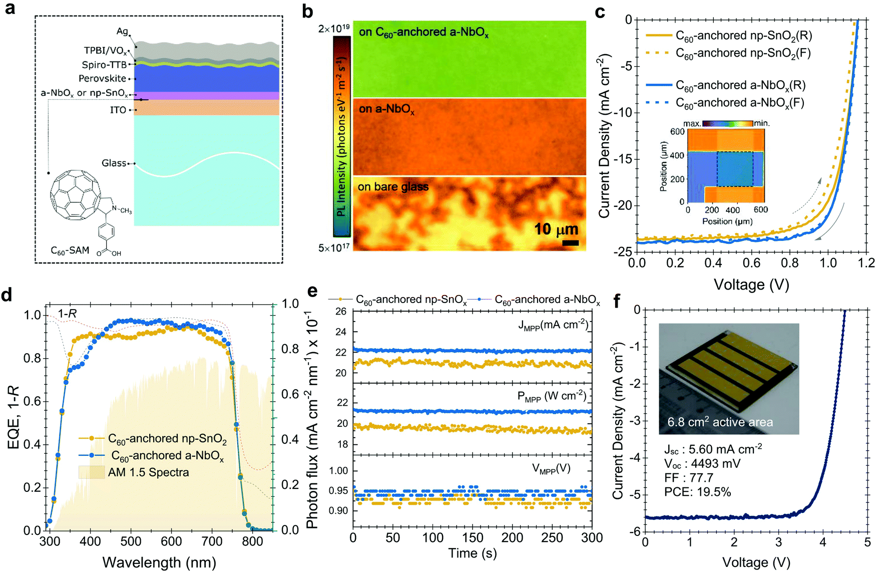 | ||
| Fig. 2 (a) Device architecture of single-junction PSCs with the chemical structure of the SAM molecule used in this study. (b) PL images of the perovskite layers on various ESL substrates. (c) J–V characteristics of the champion single-junction PSCs for np-SnOx and a-NbOx based devices and (d), corresponding EQE spectra (the dashed lines represents the 100 − R data). Note that the devices results here are reported with magnesium fluoride antireflection layer on glass side. In panel (c), the marked area in the inset image shows the LBIC image of the 0.1 cm2 PSCs. (e) MPP tracking of the np-SnOx and a-NbOx based PSCs at room temperature by using a three-point perturbation method. (f) J–V characteristics of the mini-module based on four series-connected cells. The inset fig. in panel (f) shows the photograph of the rear side of the mini-module. Note that all reported perovskite absorbers in this figure have 1.61 eV bandgap. | ||
Taking the advantage of low parasitic absorption of a-NbOx layers, ESL-side illuminated single-junction devices show a high short-circuit current density (JSC) of 24 mA cm−2, which is higher than their np-SnOx-based counterparts. These results are confirmed by external quantum efficiency (EQE) measurements, as shown in Fig. 2d (23.3 mA cm−2 from the integrated current density from EQE, within a 5% margin of equipment error). The average statistical distribution of the JSC results also confirms this observation, as shown in Fig. S13 (ESI†). Spectrally weighted absorptance values reveal that C60-anchored a-NbOx and np-SnOx has negligible absorption within the 290–850 nm range (0.65 and 1.02 W m−2 nm−1, respectively). 1 − R (R is reflectance) measurements from the whole device stack show that the PSCs based on such stacks suffer from similar R losses (112.6 and 116.9 W m−2 nm−1, respectively). In conclusion, high JSC values is mainly due to efficient charge collection as evidenced by EQE measurements (Fig. 2d).
Further, C60-anchored a-NbOx devices provide ∼4% absolute higher fill factor (FF) values on average compared to C60-anchored np-SnO2 counterparts. To understand this difference, we simulated the electric-field distribution across the device profile, which is governed by the built-in voltage (Vbi), with different biasing voltages, as discussed in Note S6 (ESI†). Considering that the perovskite/HSL interface is identical for all cases, the low voltage drop at this interface can be attributed to a high shunt and low contact resistivity of the overall stack and a higher Vbi (Fig. S15, ESI†). In an ideal case, the charge separation process is evidently more efficient if the internal electric field is stronger. Accordingly, we observed that a-NbOx based devices show a higher electric-field ratio between the ESL/perovskite and the perovskite/HSL interface, and overall lower voltage losses at the perovskite/HSL interface (see Fig. S16, ESI†). This implies an improved contact quality at the ESL/perovskite interface, which we assign to the high negative fixed-charge density of a-NbOx.46 C60-anchoring further improves the electric-field ratio and provides effective passivation at the perovskite/ESL interface.32 The relatively lower diode ideality factor of a-NbOx based devices (n = 1.23) than that of np-SnOx-based devices (n = 1.35) suggests that in the former case the recombination occurs predominantly in the quasi-neutral region rather than in the space-charge region of the device. (Fig. S18, ESI†). Here, the high negative fixed-charge density of a-NbOx may enhance the drift region in ESL/perovskite devices, which in turn leads to enhanced charge extraction and less recombination. We attribute this behavior to the high dipole moment at the a-NbOx/perovskite interface. Specifically, C60–SAM anchoring on the a-NbOx surface increases the negative charge density at the ESL/perovskite interfaces which leads to a further increases in dipole moment and electric field (see Note S6, ESI†).
Surprisingly, the FF values of the devices are not significantly affected by increasing the thickness of the a-NbOx layers up to 75 nm (Fig. S14, ESI†). Typically, metal oxide-based charge transport layers give the best PCE values when their thickness is limited to <30 nm due to their poor conductivity.47–50 We hypothesize that the absence of deep-level defect states in the bulk of the a-NbOx films, together with its thickness-independent high negative fixed-charge density allows the use of thicker films. Indeed, DFT calculations of the electronic density of states (DOS) as a function of energy demonstrate that O vacancies do not create states within the bandgap of a-NbOx. Instead, the defects shift the highest occupied states at the bottom of the CBM of the material, resulting in enhanced n-type conductivity (Note S3, ESI†). In contrast, O vacancies in tetragonal np-SnOx introduce energy levels within the bandgap of the material (Fig. S7, ESI†) and can thus act as carrier trap sites. All these results underline the efficient electron selective character of the C60-anchored a-NbOx films.
Differences between the reverse (VOC to JSC) and forward (JSC to VOC) scan are a persistent problem of the n–i–p PSCs. The potential reasons for such observed hysteresis in the case of our devices are investigated in detail in Note S8 (ESI†). More generally, we mitigated this issue by balancing the charge extraction speed at both ends of the contacts by implementing 2D/3D passivation on top of the perovskite surface (i.e. hole-collecting side), and C60-anchoring to the a-NbOx (i.e. electron-collecting side), as well as improving the perovskite crystallinity by using urea as an additive. We verified our results with stabilized power output values measured by the three-point perturbation MPP tracking method (see algorithm in Note S7, ESI†), shown in Fig. 2e (21.3% for a-NbOx and 19.9% for the np-SnOx based devices). Finally, we demonstrate the implementation of large-area deposited C60-anchored a-NbOx layers by fabricating a mini-module with a 6.8 cm2 active area, which consists of four series-connected cells. The mini-module delivered a PCE of 19.5% (active area) with a FF of 77.7%, (the J–V curve is shown in Fig. 2f), demonstrating the scalability of the C60-anchored a-NbOx layers.51
Perovskite/silicon tandem solar cells on double-side textured silicon cells
We fabricated micrometer-thick perovskite films via solution processing on the C60-anchored a-NbOx ESL (see processing details in Fig. S21, ESI†). The high perovskite crystal quality and uniformity is evidenced by the high spatial uniformity of the current collection from the tandem devices by light-beam-induced-current (LBIC) imaging (Fig. 3a). As can be seen from the cross-sectional SEM images in Fig. 3b, the perovskite layer has full end-to-end coverage on the micron-scale pyramids without leaving any uncovered pyramid or void at the interface. We verified the homogenous distribution of the perovskite elements by energy-dispersive X-ray spectroscopy (EDX) mapping from a slice of cross-sectional TEM images shown in Fig. 3c. Notably, by utilizing large-area uniform sputtered a-NbOx ESLs (as shown in Fig. S22, ESI†) with self-anchored C60, we eliminated the chemical solubility challenge of the ESL during perovskite processing as shown in Fig. S23 (ESI†). The carboxylic-acid-terminated anchoring group of the C60–SAM interacts with the a-NbOx surface thanks to its strong affinity and prevents the washing away of the C60 layer during the perovskite deposition.52 Also, the high lateral resistivity of the a-NbOx film impedes the flow of shunt currents on textured interfaces.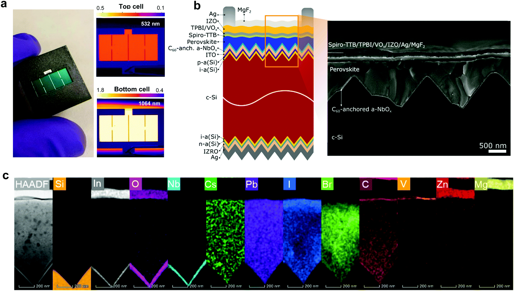 | ||
| Fig. 3 (a) The masked photograph, and LBIC images of the perovskite/silicon tandem solar cells with an excitation wavelength of 532 and 1064 nm. The scale bar shows the signal intensity. (b) Schematic of the device architecture with SEM cross-section view. (c) HRTEM images and EDX elemental mapping of the representative elements for each layer of the fabricated stack. | ||
For the HSLs, we first tested conventional Li-doped spiro-OMeTAD but expectedly, this resulted in considerable parasitic absorption in the range of 300-430 nm and a modest tandem JSC of 17.5 mA cm−2 (see Fig. S24, ESI†) due to its considerable required thickness (conventionally ∼150 nm) (Fig. 4a). To circumvent this issue, we used thermally evaporated, conformal, and thin HSLs such as spiro-TTB (∼25 nm) and TaTm (∼50 nm). Here, we successfully adopted a strong electron acceptor dopant, F6-TCCNQ to the evaporated HSLs (host), which is evident from the absorption peak in the 450–570 nm range (see Fig. S25a, ESI†) – due to the π–π*-transition of the cations/charge transfer (CT) states within the HSL.53,54 The overall parasitic absorption of the optimally doped HSLs is much less than for conventional spiro-OMeTAD (Fig. 4a). The observed near infrared (NIR) absorption peak of the spiro-TTB at ∼950 nm can be attributed to the F6-TCNNQ anion; this peak is not seen for TaTm.55 However, TaTm strongly absorbs in the blue and limits the response of the perovskite subcell (Fig. 4a). Table 1 summarizes the device characteristics of the single-junction PSC (based on 1.68 eV) with various ESLs. Upon doping, the ionization potential of the HSLs is shifted down as shown in Fig. 4b and this leads to an increased VOC. Overall, with these improvements, using doped spiro-TTB, we fabricated n–i–p tandems with higher perovskite subcell JSC values (20.2 mA cm−2 by EQE) compared to their p–i–n counterparts (19.1 mA cm−2) (Note S11, ESI†) with VOC values of >1.8 V.
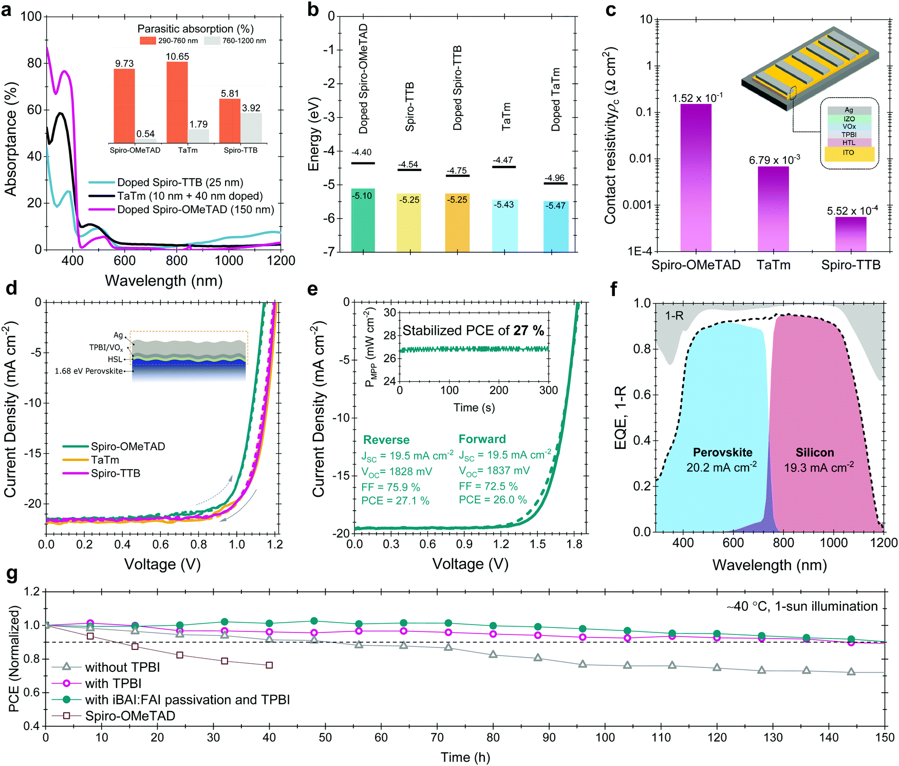 | ||
| Fig. 4 (a) Absorptance spectra of the doped spiro-OMeTAD, spiro-TTB and TaTm HSLs used in the devices. The inset figure shows the parasitic absorption of the layers at different wavelength range. We choose 760 nm as a crossover point of subcells. (b) The WF and VBM values of the various HSLs used in this study and (c) contact resistivity values for top contact stacks with these HSLs. The inset figure shows the sketch of the TLM contact pads and the contact stack. (d) Corresponding J–V curves based on 1.68 eV single-junction perovskites from glass side illumination. (e) J–V curve of the perovskite/silicon tandems and (f) corresponding EQE of this device. The gray shaded area in the EQE graph shows the 1 − R data. The inset graph in e represents the stabilized device parameters achieved by the MPP tracking method. (g) 150 h T90 stability results of glass/glass encapsulated tandems under 1-sun continuous illumination and J–V scans at every 8 hours. Between the measurements the devices were kept at MPP voltage with the three-point perturbation method. During the stability measurements, devices were kept at ∼40 °C as explained in Fig. S34 (ESI†). | ||
| HSL | Scan direction | V OC (mV) | J SC (mA cm−2) | FF (%) | PCE (%) |
|---|---|---|---|---|---|
| Spiro-OMeTAD | V OC to JSC | 1142 | 21.4 | 76.5 | 18.8 |
| J SC to VOC | 1148 | 21.6 | 75.5 | 18.8 | |
| TaTm | V OC to JSC | 1208 | 21.8 | 75.1 | 19.7 |
| J SC to VOC | 1201 | 21.9 | 75.4 | 19.8 | |
| Spiro-TTB | V OC to JSC | 1200 | 21.6 | 76.6 | 19.8 |
| J SC to VOC | 1193 | 21.7 | 76.6 | 19.8 |
We found that a-NbOx does not induce a considerable contact resistivity as confirmed by the J–V curves of the SHJ bottom cells and the contact resistivity values by transmission line measurements (TLM, see Fig. S27, ESI†), which facilitates high FF values. Also, among various HSL stacks, spiro-TTB-based ones give the lowest contact resistivity, as shown in Fig. 4c. The J–V characteristics of the single-junction devices for various HTLs (Fig. 4d) and monolithic tandems with optimized spiro-TTB are shown in Fig. 4e which shows high batch-to-batch reproducibility (see Fig. S28, ESI†). Notably, we enhance the NIR response of the tandems by reducing the reflection losses owing to the double-side textured nature of the SHJ bottom cells (Fig. S29, ESI†). To balance the JSC of top and bottom cells, we use a 1.68 eV bandgap perovskite obtained by increasing the Br percentage from 15% to 25%, which is in the range of an ideal top cell bandgap.1 To minimize the hysteresis behavior, which is discussed in Note S8 (ESI†), we utilized a mixed 2D/3D passivation treatment strategy (see structural details in Fig. S30, ESI†) since this enables non-continuous 2D layers on the perovskite surface by passivating the surface defects, while still allowing charge transport via 3D perovskite pathways. By applying iso-butylammonium iodide, (iBAI) and formamidinium iodide (FAI) mixed passivation, we decreased the number of surface defects and mitigated ion migration, thereby significantly decreasing the hysteresis of the device (see Fig. 4e and Fig. S31, ESI†).56
Furthermore, we minimized the parasitic absorption losses in the blue range of the solar spectrum by combining thermally-evaporated spiro-TTB with atomic layer deposited VOx in the hole selective contact stack (see discussion on buffer layer selection in Note S13, ESI†) as well as by replacing the rear ITO with Zr-doped indium oxide (IZRO)57 (for a lower extinction coefficient) and by thinning down the front indium zinc oxide (IZO) from 100 to 70 nm (Fig. S33, ESI†). As a consequence of improved light management (Fig. 4f), combined with enhanced charge extraction, we record a significant improvement from the last reported perovskite/silicon tandem in the n–i–p configuration on a SHJ bottom cell (which was ∼22%) and achieved a 27% efficient monolithic tandem performance from such devices, which is one of the highest PCEs reported in either the n–i–p (see Table S7, ESI†) or p–i–n tandem configurations.2–5 We confirmed this PCE value by MPP measurements under continuous illumination (inset of Fig. 4e).
We also performed stability tests of the tandem devices under 1-sun continuous illumination and intermittent J–V scans. For this, we first encapsulated devices between two glass sheets with butyl rubber as edge sealant, shown in Fig. S34 (ESI†). The optimized devices maintained 90% of their initial VOC and FF values for 150 h (Fig. 4g). In the literature, n–i–p devices are frequently reported to have short operational stability due to fast degradation of the doped HSL.33,36,37 To identify potential degradation mechanisms of our HSL stacks, we performed a set of stability measurements. We found that the spiro-TTB/VOx interface appears to be sensitive to degradation due to Lewis acid quenching of radical anions and di-anions of the F6-TCNNQ, with a consequence of the free electron lone pairs that act as a Lewis base. At the HSL/VOx interface, vanadium centers act as a Lewis acid, and attract and coordinate highly electron-rich nitrogen atoms of F6-TCNNQ, thereby suppressing its activity. From our stability test with single-junction test structures, we found that elevated temperature is the primary reason for this accelerated degradation (see Fig. S35, ESI†). This stems from the accumulation of quenched dopants at the VOx interface at elevated temperature.58 To mitigate this issue, we introduced a 2 nm thin layer of 2,2′,2′′-(1,3,5-Benzinetriyl)-tris(1-phenyl-1-H-benzimidazole), TPBI, which effectively prevented the interaction between F6-TCNNQ and VOx without jeopardizing the charge transfer due its ultra-thin nature.
Efficient charge extraction at C60-anchored a-NbOx and perovskite interfaces
We performed time-resolved photoluminescence (TRPL) spectroscopy measurements to analyze the charge carrier dynamics at the perovskite/ESL interface. We found that the PL lifetime of the perovskite in the quartz/a-NbOx/perovskite sample is significantly longer than that of both the quartz/np-SnOx/perovskite and the quartz/perovskite sample structure (Fig. 5a). We note that the substrate could affect the perovskite film formation and thereby the perovskite defect distribution which in turn could alter the PL lifetime of the perovskite films, as shown in Fig. 2b. We hypothesize that the reason for the longer PL lifetime is two-fold: (i) the absence of deep-level defects at the a-NbOx/perovskite interface, and (ii) the dependency of the PL lifetime of the absorber on the carrier concentration (Ne) of the charge transport layers, where low Ne values lead to less quenching of the PL lifetime.19,59 Here, compared to np-SnOx, a-NbOx films have a seven orders of magnitude lower carrier concentration than np-SnOx, which appears to be the reason for this behavior (Table S1, ESI†).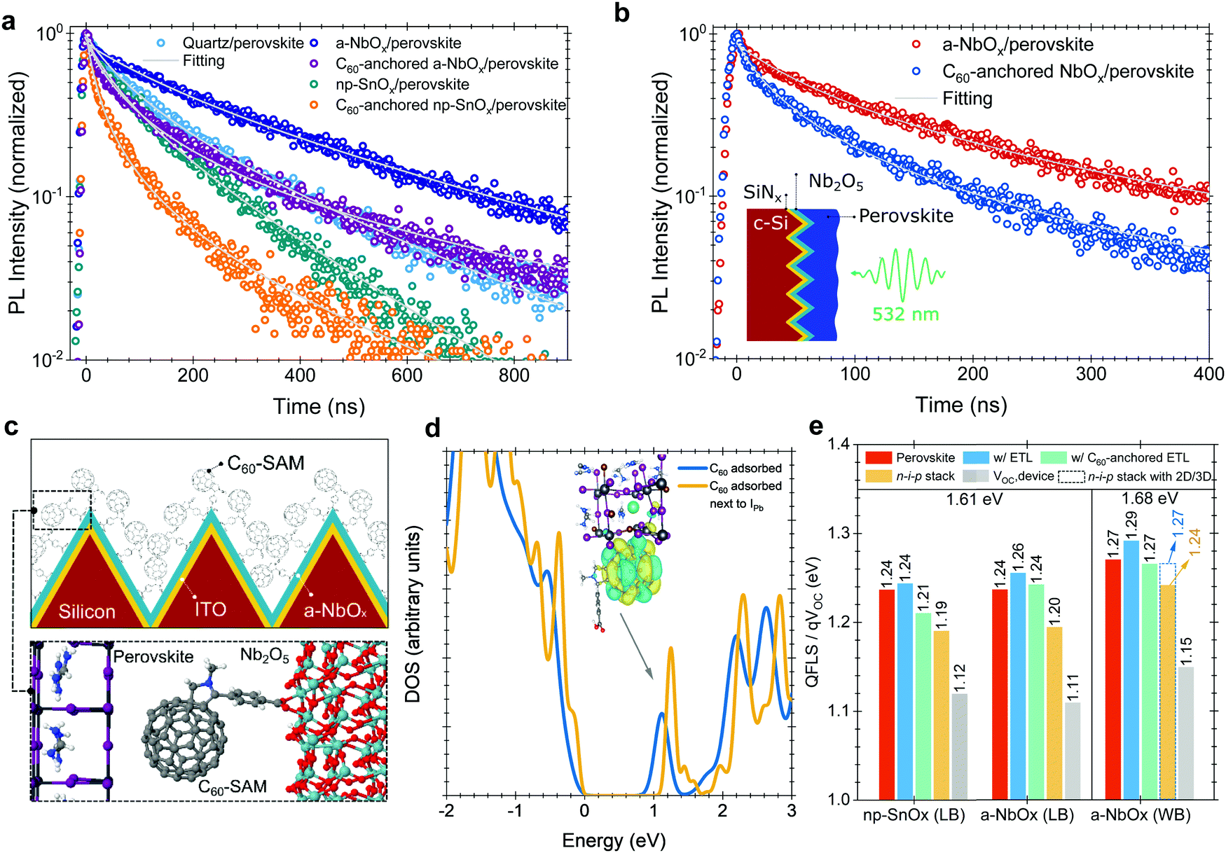 | ||
| Fig. 5 The PL decay of (a) 1.61 eV perovskite samples on quartz, (b) 1.68 eV perovskites on textured c-Si/SiNx substrates. The decays were probed at ∼768 and ∼738 nm across a ∼20 meV range for 1.61 and 1.68 eV perovskites, respectively. All the samples were excited at 532 nm with a fluence 0.5 μJ cm−2 and a repetition rate of 1 kHz. (c) Schematics of the self-assembly process. The magnified area shows the proposed model for the interaction of the pyrrolidine group of a C60–SAM molecule with a-NbOx and the electronic coupling of C60 molecule with perovskite lattice. (d) Electronic density of states (DOS) for the structure shown in I and for C60 molecule physisorbed on a Pb–I terminated perovskite surface with and without an Pb–I anti-site defect. The zero energy is at the valence band maximum of the perovskite. Peaks shown with arrow points out C60-related empty states in the bandgap. (Nb: dark gray, O:red, C: gray, N: blue, H:white, Pb: dark gray, I: purple, Br: dark orange, Cs: cyan spheres). (e) QFLS values of perovskite and perovskite/transport layer stacks, and VOC values of the devices for 1.61 eV and 1.68 eV bandgap perovskites. Values extracted from the absolute PL data using a hyperspectral imaging system with the excitation at 532 nm under 1-sun illumination condition (LB: low bandgap, WB: wide bandgap). | ||
We note that the PL lifetime of C60-anchored a-NbOx/perovskite sample is almost three times that of the C60-anchored np-SnOx/perovskite sample. The shorter PL lifetime of the latter can be caused by either efficient charge extraction from the perovskite to the ESL or increased recombination at the interface.19 To clarify the origin, we determined the k1 values, which are related to trap-assisted recombination, for samples with and without C60-anchored ESLs. We found that C60-anchoring on np-SnOx and a-NbOx resulted in lower k1 values than observed for neat ESLs and overall less trap-assisted recombination. All values are listed in Table 2.
| Sample | k 1 (s−1) | k 2 (cm3 s−1) | t (ns) |
|---|---|---|---|
| Quartz/perovskite (1.61 eV) | 2.8 × 10⁶ | 2.2 × 10⁻¹⁰ | 172 |
| Quartz/a-NbOx/perovskite (1.61 eV) | 1.8 × 10⁶ | 8.1 × 10⁻¹¹ | 384 |
| Quartz/C60-anchored a-NbOx/perovskite (1.61 eV) | 1.0 × 10⁶ | 4.3 × 10⁻¹⁰ | 107 |
| Quartz/np-SnOx/perovskite (1.61 eV) | 4.4 × 10⁶ | 2.7 × 10⁻¹⁰ | 130 |
| Quartz/C60-anchored np-SnOx/perovskite (1.61 eV) | 2.6 × 10⁶ | 1.3 × 10⁻⁹ | 36 |
| Textured c-Si/SiNx/a-NbOx/perovskite (1.68 eV) | 1.8 × 10⁶ | 2.5 × 10⁻¹⁰ | 140 |
| Textured c-Si/SiNx/C60-anchored a-NbOx/perovskite (1.68 eV) | 1.8 × 10⁶ | 6.7 × 10⁻¹⁰ | 57 |
To evidence the C60-anchoring on the a-NbOx films on textured substrates, we performed TRPL measurements also on wide bandgap (1.68 eV) perovskite absorbers deposited on textured c-Si/SiNx/perovskite stacks, where SiNx is silicon nitride, which is used to electrically isolate the Si wafer (Fig. 5b). Here, we found the PL lifetime to be reduced from 140 ns to 57 ns in the case of C60-anchoring, confirming the enhanced charge extraction properties of the self-assembled layer on textured interfaces, which is in line with the measurements performed on the 1.61 eV bandgap perovskites on quartz substrates.
For the C60–SAM anchoring, the pyrrolidine group of the C60–SAM molecule strongly interacts with the metal oxide ESLs (Fig. 5c), while its C60 component interacts with (negatively-charged) iodide ions, which originate from non-coordinated Pb or Pb–I anti-site defects. To further elaborate on the role of the C60–SAM cage, we modeled the adsorption of such a cage (with and without the pyrrolidine tail) on the (001) surface of formamidinium lead iodide (FAPbI3), as well as on the (001) surface of a mixed perovskite of the composition FA0.70MA0.20Cs0.10PbI2.50Br0.50 with DFT calculations. In these cases, the fullerene moiety physisorbed on the perovskite (with a significant binding energy of about 1.79 eV for C60 on FAPbI3), creating empty energy states inside the energy bandgap of the FAPbI3. It should be noted that, in the FA0.70MA0.20Cs0.10PbI2.50Br0.50 case, the C60-related state is also below a gap level associated with the common Pb–I anti-site perovskite defect.
In agreement with experiments, our DFT calculations (Note S3, ESI†) suggest that the empty C60-related gap states can extract electrons from the conduction band or electron traps (related to, e.g., Pb–I antisite defects) of the perovskite (Fig. 5d) and pass them on to the NbOx side through the firmly attached pyrrolidine tails. On the ESL side, the role of O vacancies (Ov) is crucial for the efficient extraction of electrons. In the SnOx case, Ov defects create charge trap states (Fig. S7, ESI†) that can hinder carrier transport, which is in line with space-charge-limited-current (SCLC) and impedance spectroscopy measurements (Note 14 and 15, ESI†). On the other hand, in the NbOx case, Ov shifts the highest occupied states into the bottom of the conduction band. This effect is also found for O-deficient NbOx terminations (Fig. S6, ESI†), and persists even after C60-anchoring. At this level of theory, Ov enhances the n-type conductivity of the material, in agreement with the aforementioned experimental observations.
To support our VOC results, we performed absolute PL measurements (Fig. S38, ESI†) to determine the quasi-Fermi-level-splitting (QFLS), which represents the maximum achievable VOC from the perovskite absorbers with and without contact stacks. Herein, C60-anchored a-NbOx based stacks show 1.24 eV, while np-SnOx devices show 1.21 eV for 1.61 eV perovskites (Fig. 5e), in line with the results of the TRPL measurements (Fig. 5a), and also the VOC values of the devices (Table S4, ESI†). The presence of the C60-anchoring improves the charge extraction in both a-NbOx and np-SnOx samples but it lowers the QFLS values due to energetic issues, as discussed in Note S4 (ESI†). However, in devices, the measured VOC values are lower than the QFLS values. According to our measured UPS and IPES data, both a-NbOx and np-SnOx layers add a 20 meV potential barrier at the interface to perovskite after C60-anchoring. However, several studies reported that this level of CB offset is needed to suppress interfacial recombination due to the reduced back-transfer recombination and improved FF.60–62
Conclusion and outlook
Here, we overcome the persistent processing limitations of n–i–p configuration perovskite/silicon tandem solar cells by combining on pyramidal textured SHJ bottom cells a RF-sputtered a-NbOx with conformal C60-anchoring as ESL, micrometer-thick solution-processed perovskites and a highly transparent conformal HSL stack. All these advancements enabled 27% efficient perovskite/silicon monolithic tandems in n–i–p configuration, which is a >5% absolute increment over the prior state of the art on SHJ bottom cells. Our demonstration of an efficient n–i–p tandem device platform opens new pathways to propel the efficiency of perovskite/silicon tandems beyond the thermodynamic limit for single-junction solar cells. For instance, thermally-evaporated C60 ESL for p–i–n configuration stands out unrivaled so far, even though this material causes strong parasitic absorption. On the other hand, there are many small molecule HSLs in the literature which have remained unexplored in n–i–p tandem solar cells to improve the device optics further and overall reaching to >20 mA cm−2 tandem devices. Furthermore, to overcome the limited long-term operational stability of the perovskite/silicon tandems, 2D-perovskite passivation strategies can be utilized which has been a challenge with p–i–n devices due to energetic alignment problems of the 2D perovskites with the widely used C60 ESLs. Also, bifacial tandem devices can be more relevant in the n–i–p configuration, since the bottom cell utilizes an n-type contact at its back, high refractive index but lower conductivity TCOs can be utilized. Beyond these opportunities, our developed hole selective contact stack will also enable progress in perovskite/perovskite tandems by eliminating the air exposure requirement of moisture-sensitive Sn-based perovskites during HSL processing, which has been an issue so far. Lastly, the n–i–p tandem platform enables utilization of tandems as a photocathode in efficient solar-driven water splitting applications for hydrogen generation since this application requires electrons to be extracted from the cathode side with voltage values of >1.4–1.8 V, as well as high current densities.Experimental section
Deposition of a-NbOx and np-SnO2 layers
a-NbOx layers were deposited by radio frequency (RF, 13.56 MHz) magnetron sputtering from the stoichiometric a-NbOx target (Plasmaterials, 99.95% purity) at room temperature using Angstrom Engineering EvoVac system at 1.97 W cm−2 power density. The Argon gas was supplied to the chamber with 20 sccm. The deposition rate of the films was 0.15 Å s−1. The base pressure for deposition was <2 × 10⁻⁶ Torr, and the deposition pressure was 3 mTorr. Before each deposition, the target was pre-sputtered for 10 min to remove the contamination layer, if any, on the surface of the target. For homogenous deposition, substrate rotation was provided. The substrate was not heated or cooled intentionally. np-SnO2 layers were deposited by spin-casting of aqueous Alfa Aesar nanoparticle suspension at 3000 rpm for 30 s (with 3000 rpm s−1 ramp rate), and resultant films were annealed in ambient air at 150 °C for 30 min. Prior to np-SnOx deposition, 10 min UV-ozone treatment was applied on ITO/glass substrates. However, this step was not used prior to the deposition of a-NbOx layers.C60–SAM modification of a-NbOx layers
C60-based self-assembled monolayer (C60-COOH-SAM, CAS No.: 631918-72-4, Luminescence Technology Corp.) dissolved in chlorobenzene and stirred vigorously overnight. Later, the stock solution filtered using a 0.2 μm PTFE filter. The C60–SAM was spun on a-NbOx or np-SnOx at 3000 rpm for 60 s with a 3000 rpm s−1 ramp rate. Before this, the surface of the a-NbOx layer is treated with 1 mg mL−1 concentrated aqueous potassium chloride solution.Fabrication of the single junction perovskite solar cells
The mixed Cs0.05MA0.15FA0.8Pb(I0.85Br0.15)3 perovskite precursor solution was prepared using FAI (0.96 M), MABr (0.18 M), CsI (0.06 M) PbI2 (1.04 M), and PbBr2 (0.185 M) materials in a mixed solvent of 800 μL DMF and 200 μL DMSO. The perovskite solution was spin-coated on electron transport layers (either 20 nm np-SnOx or 50 nm a-NbOx) at two-step: 2000 rpm for 10 s and 4000 rpm for 30 s. For antisolvent quenching, 150 μl chlorobenzene was dropped through the center of the substrates 10 s prior to the end of the spin-coating process. After that, films were transferred immediately onto 100 °C preheated hotplate and annealed for 30 min. 25 nm Spiro-TTB was deposited by thermal evaporation as defined below. 10 nm ALD deposited vanadium oxide (VOx) was deposited using via the Picosun ALD tool using vanadyl-tri-isopropoxide (VTIP, precursor was kept 80 °C) and H2O as precursors and substrate at 90 °C. 100 nm of Ag layers were thermally evaporated on top of HSL stack by thermal evaporation in an Angstrom Engineering EvoVac deposition system. 100 nm of MgF2 is evaporated (if stated) as an anti-reflective layer with 1 Å s−1 deposition rate to minimize the reflection losses for both np-SnOx and a-NbOx layers.Fabrication of the silicon bottom cell
SHJ bottom cells are fabricated on float-zone double-side-textured four inches wafers (n-doped, resistivity 1–5 Ω cm−1, thickness 250–280 μm). The texturing process is done in an alkaline solution to get randomly distributed pyramids and cleaned in RCA1 and RCA2 solution. The size of the pyramids is controlled by adjusting the alkaline concentration and the process temperature. Before the PECVD depositions, the wafers are dipped in 5% hydrofluoric acid solution to remove the native oxide layer. The intrinsic, p, and n silicon amorphous layers are deposited in a PECVD cluster (Indeotec Octopus – 2) with a thickness of 8, 6, and 13 nm, respectively. The back electrode is realized by sputtering sequentially ITO and Ag (150 and 250 nm, respectively) in the PVD part of the Octopus cluster. In case of IZRO rear TCO, the recipe given in our previous publication is used.57 The ITO recombination junction (15 nm) is sputtered in the same tool. Prior to the a-NbOx deposition, and after a-NbOx deposition, the wafers are annealed at 190 °C for 10 min to recover the sputtering damage.Fabrication of the perovskite top cell
To achieve n–i–p configuration perovskite top cells, a-NbOx layers (20 nm on the textured surface) is deposited by RF sputtering as the ESL and modified by C60–SAM as defined above. Before C60–SAM deposition the samples were annealed at 190 °C in glove box for 20 min to mitigate the plasma damage on the bottom cells. On top, the Cs0.05MA0.15FA0.8Pb(I0.75Br0.25)3 perovskite is deposited from a 1.7 M solution in DMF![[thin space (1/6-em)]](https://www.rsc.org/images/entities/char_2009.gif) :DMSO (4:1) via 3-step spin coating process (see Note S9 for details, ESI†). For better crystallization, we added 0.25 mg mL−1 urea (Merck) to the precursor as we introduced previously.63 To prepare 2D/3D mixed passivation solution, iBAI and FAI (and other organohalides such as MAI, MACl) was mixed in isopropyl alcohol with total solution concentration of 10 mM. Here, the iBAI and FAI wt ratio in solution 3:1. After dissolving, the solutions were filtered with PTFE filters (0.2 mm) and spin casted on previously fabricated perovskite films (at room temperature) at 5000 rpm for 20 s. No annealing step was applied. 25 nm Spiro-TTB (Lumtec, Sublimed, >99%, in alumina crucible) and F6-TCNNQ (Lumtec, >99%) were cosublimed at 260–280 °C and 160–170 °C, respectively by the Angstrom EvoVac evaporation system. The deposition rate was controlled by QCM sensors and adjusted to obtain the desired doping concentrations. For the host materials (spiro-TTB and TaTm, here TaTm is from TCI) the deposition rate was 0.8 Å s−1 in alumina crucible. The optimal dopant evaporation rate was 0.1 Å s−1, which represents the 11.1 wt% doping ratio. HSLs were capped with 2 nm of thermally evaporated TPBI (Ossila, Unsublimed >98.0%, 0.2 Å s−1, in alumina crucible), and 10 nm VOx is deposited by ALD as defined above. 70 or 100 nm IZO top electrode was sputtered in the Angstrom EvoVac sputtering system with an RF of 42 W at (60 and 40 Ω sq−1, repsectively), as defined in the text. 350 nm Ag contacts were evaporated through a shadow mask using Angstrom EvoVac thermal evaporator with 2.5 Å/s deposition rate. Finally, 120 nm of MgF2 is evaporated with the same equipment as an anti-reflective layer with 1 Å s−1 deposition rate. Device layouts are given in Fig. S39 (ESI†).
:DMSO (4:1) via 3-step spin coating process (see Note S9 for details, ESI†). For better crystallization, we added 0.25 mg mL−1 urea (Merck) to the precursor as we introduced previously.63 To prepare 2D/3D mixed passivation solution, iBAI and FAI (and other organohalides such as MAI, MACl) was mixed in isopropyl alcohol with total solution concentration of 10 mM. Here, the iBAI and FAI wt ratio in solution 3:1. After dissolving, the solutions were filtered with PTFE filters (0.2 mm) and spin casted on previously fabricated perovskite films (at room temperature) at 5000 rpm for 20 s. No annealing step was applied. 25 nm Spiro-TTB (Lumtec, Sublimed, >99%, in alumina crucible) and F6-TCNNQ (Lumtec, >99%) were cosublimed at 260–280 °C and 160–170 °C, respectively by the Angstrom EvoVac evaporation system. The deposition rate was controlled by QCM sensors and adjusted to obtain the desired doping concentrations. For the host materials (spiro-TTB and TaTm, here TaTm is from TCI) the deposition rate was 0.8 Å s−1 in alumina crucible. The optimal dopant evaporation rate was 0.1 Å s−1, which represents the 11.1 wt% doping ratio. HSLs were capped with 2 nm of thermally evaporated TPBI (Ossila, Unsublimed >98.0%, 0.2 Å s−1, in alumina crucible), and 10 nm VOx is deposited by ALD as defined above. 70 or 100 nm IZO top electrode was sputtered in the Angstrom EvoVac sputtering system with an RF of 42 W at (60 and 40 Ω sq−1, repsectively), as defined in the text. 350 nm Ag contacts were evaporated through a shadow mask using Angstrom EvoVac thermal evaporator with 2.5 Å/s deposition rate. Finally, 120 nm of MgF2 is evaporated with the same equipment as an anti-reflective layer with 1 Å s−1 deposition rate. Device layouts are given in Fig. S39 (ESI†).
Characterization of the photovoltaic performances
Single junction PSCs and tandem solar cells were tested under standard test conditions (100 mW cm−2, AM1.5G, 25 °C). Single junction PSCs were tested with ABET Technologies Sun 3000 Solar Simulator equipped with Keithley 2400 source meter. The light intensity was calibrated using a certified reference cell with a KG5 filter (RERA Solutions, calibrated at Radboud University Nijmegen). Devices were tested at a 200 mV s−1 scan rate. Devices had a 0.1 cm2 square active area (as shown in the inset of Fig. 2c). Note that the reverse scan is from VOC to JSC (1.25 V → −0.1 V), and the forward scan is from JSC to VOC (−0.1 V → 1.25 V). No preconditioning protocol has been used before the measurement.J–V measurements of the tandem solar cells were performed using Wavelabs Sinus 220 LED-based solar simulator. To calibrate spectrum, we used Fraunhofer ISE certified calibration cell (without a filter). We did not apply a spectral mismatch factor. The illumination area of the devices was 1.03 cm2, which is determined by the laser cut shadow mask coated with black paint. Maximum power point tracking (MPPT) measurements were performed via the homemade LabView® based software using a three-point weight comparison method (for details, see Note S7, ESI†). The device measurements were performed at 200 mV s−1 scan speed. EQE measurements were performed using PV-Tools LOANA equipment. When measuring perovskite top cells, the tandem devices were light-biased by IR LEDs (930 nm); when measuring silicon bottom cells, the tandem devices were light-biased by a blue LED to saturate the subcells. To enable the near short-circuit conditions, MPP voltages were applied on the devices. All device characterizations were performed at ambient air with RH ∼50% and without any encapsulation.
Stability tests
Devices were encapsulated between two glasses (3 mm low iron glasses) with 10 mm wide and 1 mm thick butyl rubber Solargain® edge sealant with desiccant (Quanex, SET LP03), which were laminated at 100 °C. The illuminated area (1 cm2) of the cells was determined by non-transparent black tape on top of the front glasses. Indoor stability measurements were performed with Lot Oriel class AAA solar simulator equipped with a Xenon lamp. The encapsulated modules were kept at 25 °C cooled by refrigerated circulation stage. For MPP tracking measurements, devices were kept under MPP load via a three-point perturbation method, and J-V scans were performed every three hours.Structural and optical characterizations
Atomic force microscopy (AFM) images were obtained with tapping mode using a Digital Instruments Multimode AFM (Veeco Metrology Group). A probe (TAP150A, Veeco) with a force constant of ∼5 N m−1 was used. X-ray diffraction patterns were obtained using a Bruker D8 Advance X-ray diffractometer (CuKα1 radiation, λ = 1.5406 Å) from 10° to 80° (2θ) with a scan speed of 3° min−1. The Scanning transmission electron microscopy (STEM) images were taken by an FEI Themis-Z transmission electron microscope operated at 300 kV. Energy Dispersive X-ray Spectroscopy studies were performed with a Bruker super-X EDS detector. TEM lamellas were prepared on an FEI Helios G4 FIB/SEM dual-beam system equipped with a Ga+ ion source. C/Pt layers were deposited on the surface region of interest by the Electron & Ion beam for sample protection. Samples were thinned down to a relative thickness of 80 nm using progressively decreasing ion beam energies in the FIB down to 5 keV. Contact angles were measured with a KRUSS-The Drop Shape Analyzer DSA100 system by using water as the wetting solvent. Spectroscopic ellipsometry measurements of the a-NbOx/c-Si stacks were performed by using J. A. Woollam M-2000DI at 65° and 75°. The c-Si substrate was a single-polished float-zone wafer (525 ± 25 mm), and a-NbOx film was deposited on the polished side. Such a substrate can effectively impede interference caused by light reflection from the rear side. An optical model of air/surface roughness/ a-NbOx/c-Si is used to fit the (Y,D) raw data. The impedance measurements were performed on Fluxim Paios system.UPS/XPS analysis
All the films were prepared on pre-cleaned ITO substrates as used in devices. The measurements were carried out with a UHV 0.5–1 10−9 mbar Omicron spectrometer equipped with a monochromatic Al Kα X-ray Omicron XM1000 X-ray source (hν = 1486.6 eV) operating at 389 W and a Sphera II spectrometer with a 7-channel channeltron. The survey and high-resolution spectra were collected at constant analyzer pass energies (CAE) of 50 and 15 eV, respectively. Samples (∼0.5 × 1.0 cm) were mounted in electrical contact to the Omicron style sample plate by clamping with Ta clips in contact with the sample surface, binding energy calibration and sample charging were accounted for by reference to the ambient contamination C 1s adventitious carbon, ∼284.7 eV. Samples were introduced to the chamber via a N2 filled UHV compatible transfer system from an N2 glove box where the samples were mounted to minimize ambient exposure. The spectra were analyzed with Casa XPS software. The individual peak envelopes were fitted by a Gaussian (70%)–Lorentzian (30%) (GL30) function after Shirley-type background subtraction. UPS measurements were performed in the same instrument on the same samples with a (CAE) of 10 eV, using a He (I) excitation discharge lamp (hν = 21.22eV) (Focus). A bias of −9.97 V was applied to the sample. The photoelectrons were collected at an angle of 90° between the sample and analyzer.
Time-resolved photoluminescence (TR-PL) spectroscopy
Perovskite films were deposited either on pre-cleaned quartz substrates or on ESLs (np-SnOx and a-NbOx) using the same recipe as used for device fabrication. After deposition of the layers, samples were placed in a sealed N2 chamber to avoid any changes due to photo-induced degradation. All measurements were performed at room temperature. The samples were excited with the Coherent Helios 532 nm nanosecond (ns) laser with a pulse width of 0.85 ns and a peak with a repetition rate of 1 kHz. The excitation beam at 532 nm was focused on pumping the samples, mounted inside the sealed chamber. The PL of the samples was collected by an optical telescope (consisting of two plano-convex lenses) and focused on the slit of a spectrograph (PI Spectra Pro SP2300) and detected with a Streak Camera (Hamamatsu C10910) system. The data was acquired in photon counting mode using the Streak Camera software (HPDTA). The photogenerated carrier concentration at t = 0 was calculated using the formula64 of n0 = α·f/Ephoton where α is the absorption coefficient at the excitation wavelength, f is the fluence of the laser and Ephoton is the excitation photon energy. The PL lifetimes were determined by using the general rate equation (−dn/dt = k1n + k2n2) however, excluding Auger recombination, since the initial carrier concentration was low (n0 = 4 × 1016 cm−3), where Auger recombination is negligible in perovskites.65Absolute PL measurements
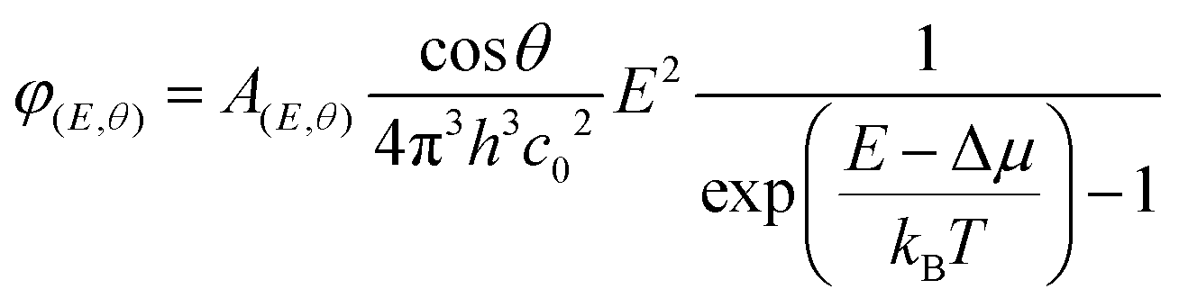
Perovskite films were deposited on pre-cleaned glass substrates or on ESLs (np-SnOx and a-NbOx) using the same recipe as used for device fabrication. The absolute PL spectra of the samples were collected using a hyperspectral imaging system coupled to a microscope with 2 nm spectral resolution (Photon etc. IMA). Samples were excited with 532 nm laser at ∼1 sun illumination condition (before the measurement, the power density of the laser was adjusted with a reference perovskite solar cell). The absolute calibration procedure of the setup is reported in detail elsewhere.66 The collected data was analyzed via home-built MatLab code using modified generalized Plank law to get quasi-Fermi level splitting using the formula:67where A(E,θ) is the absorption probability of a photon with energy E, incident at an angle θ with respect to the surface normal. Δμ and kBT are quasi-Fermi level splitting and Boltzmann constant and the temperature (equivalent to 25.7 meV at room temperature), respectively. Here, cos
 θ factor appears as the emission from the surface following Lambert's law.
Device simulations
The optical response of the single-junction PSCs was calculated based on the finite element method (COMSOL Multiphysics), where periodic boundary conditions were implemented in a unit cell.68 The linearly polarized plane wave was illuminated normally to the cell top surface. The PSC was illuminated from the top with a linearly polarized plane wave impinging normally to the cell top surface, covering the wavelength ranges from 300 nm to 800 nm (AM1.5G illumination), comprising the bandgap of PSCs. Two-dimensional device simulation of NbOx and SnOx PSCs was based on a classical drift-diffusion and Poisson's equation and solved by the finite element method (COMSOL Multiphysics) based semiconductor device simulator.69 The simulation was carried out at 300 K under one sun (AM1.5G, −100 mW cm−2) condition. The optical bandgap, thickness, and energetics (bandgaps, electron affinity) related to the active and other layers used in the simulation were obtained from the UPS/IPES measurements and listed in Note S4 (ESI†).DFT analysis
Calculations were performed with the DFT code Quantum Espresso,70 the Perdew–Wang generalized-gradient approximation exchange-correlation functional (xc),71 projector-augmented waves,72 [3] and the DFT-D2 method73 to include van der Waals interactions. The energy cutoff for the plane-wave basis was set at 100 Rydbergs. The calculation of densities of states (DOS) employed the Monkhorst–Pack scheme with Gaussian broadening and 4 × 4 × 1 k-grids.74 In total energy calculations on large supercells, only the gamma point was used for k-sampling. Structures were rendered with VESTA.75 To model O vacancies in the bulk of SnO2 and Nb2O5 we used supercells with, respectively, 71 and 111 atoms. The calculations pertaining to adsorption of pyrrolidine or C60-pyrrolidine on the (001) surface of SnOx, the (100) surface of Nb2O5, and the (001) surface of the halide perovskite used supercell slabs with, respectively, 102, 142, and 197 atoms. The large size of the supercells precluded the possibility of using post-DFT corrections in the form of a hybrid xc-functional.Author contributions
E. A. conceived the idea, designed the experiments, fabricated the devices, and conducted device characterizations, and performed optoelectronic characterizations of the fabricated layers. E. A., Y. H., M. D. B., and B. C. developed the wide-bandgap perovskite processing on textured interfaces. E. U. optimized the C60–SAM process, contributed to HSL optimizations, and performed TRPL and absolute PL (using hyperspectral imaging system) measurements and data analysis. E. U, R. A, and S. Z. contributed to the single-junction device fabrication. M. W. developed MPP tracking software and MatLab code for quasi-Fermi level splitting calculations and contribute to data analysis. F. L. supervised TRPL and absolute PL spectroscopy measurements and data analysis. L. T. performed the DFT calculations. W. R. performed two-dimensional device simulations. J. L. contributed the single-junction device fabrication and optimized the 1.61 eV perovskite absorbers, performed AFM measurements. M. D. B. performed OPAL simulations and transient photocurrent measurements. A. B. joined data interpretation of the hysteresis behavior and band levels of the layers. F. H. I. performed contact angle and SCLC measurements. A. S. S. performed the impedance analysis. F. H. I. and A. S. S. designed the mini-module contact layout. E. A. designed the tandem device contact layout. K. W. performed the XRD measurements. G. T. H. performed XPS, UPS, and IPES measurements. T. G. A., M. D. B., A. U. R., M. B. and E. V. K. fabricated the silicon bottom cells. E. A. composed the manuscript. All authors discussed the results and commented on the manuscript. S. D. W., F. L., and E. H. S. supervised the project.Conflicts of interest
The authors declare no competing interests.Acknowledgements
The authors would like to thanks to Nini Wei for the TEM images; funding: the research reported in this publication was supported by funding from King Abdullah University of Science and Technology (KAUST) under award no. OSR-CARF/CCF-3079 and award no. IED OSR-2019-4208.References
- E. Aydin, T. G. Allen, M. De Bastiani, L. Xu, J. Ávila, M. Salvador, E. Van Kerschaver and S. De Wolf, Nat. Energy, 2020, 5, 851–859 CrossRef CAS.
- F. Sahli, J. Werner, B. A. Kamino, M. Bräuninger, R. Monnard, B. Paviet-Salomon, L. Barraud, L. Ding, J. J. Diaz Leon, D. Sacchetto, G. Cattaneo, M. Despeisse, M. Boccard, S. Nicolay, Q. Jeangros, B. Niesen and C. Ballif, Nat. Mater., 2018, 17, 820–826 CrossRef CAS PubMed.
- Y. Hou, E. Aydin, M. De Bastiani, C. Xiao, F. H. Isikgor, D.-J. Xue, B. Chen, H. Chen, B. Bahrami, A. H. Chowdhury, A. Johnston, S.-W. Baek, Z. Huang, M. Wei, Y. Dong, J. Troughton, R. Jalmood, A. J. Mirabelli, T. G. Allen, E. Van Kerschaver, M. I. Saidaminov, D. Baran, Q. Qiao, K. Zhu, S. De Wolf and E. H. Sargent, Science, 2020, 367, 1135–1140 CrossRef CAS PubMed.
- M. Jošt, E. Köhnen, A. Morales Vilches, B. Lipovšek, K. Jäger, B. Macco, A. Al-Ashouri, J. Krc, L. Korte, B. Rech, R. Schlatmann, M. Topic, B. Stannowski and S. Albrecht, Energy Environ. Sci., 2019, 11, 3511–3523 RSC.
- J. Xu, C. C. Boyd, Z. J. Yu, A. F. Palmstrom, D. J. Witter, B. W. Larson, R. M. France, J. Werner, S. P. Harvey, E. J. Wolf, W. Weigand, S. Manzoor, M. F. A. M. van Hest, J. J. Berry, J. M. Luther, Z. C. Holman and M. D. McGehee, Science, 2020, 367, 1097–1104 CrossRef CAS PubMed.
- D. Kim, H. J. Jung, I. J. Park, B. W. Larson, S. P. Dunfield, C. Xiao, J. Kim, J. Tong, P. Boonmongkolras, S. G. Ji, F. Zhang, S. R. Pae, M. Kim, S. B. Kang, V. Dravid, J. J. Berry, J. Y. Kim, K. Zhu, D. H. Kim and B. Shin, Science, 2020, eaba3433, DOI:10.1126/science.aba3433.
- B. Chen, Z. J. Yu, S. Manzoor, S. Wang, W. Weigand, Z. Yu, G. Yang, Z. Ni, X. Dai, Z. C. Holman and J. Huang, Joule, 2016, 4, 850–864 CrossRef.
- A. S. Subbiah, F. H. Isikgor, C. T. Howells, M. De Bastiani, J. Liu, E. Aydin, F. Furlan, T. G. Allen, F. Xu, S. Zhumagali, S. Hoogland, E. H. Sargent, I. McCulloch and S. De Wolf, ACS Energy Lett., 2020, 5, 3034–3040 CrossRef CAS.
- E. Aydin, M. De Bastiani and S. De Wolf, Adv. Mater., 2019, 1900428 CrossRef PubMed.
- J. J. Yoo, G. Seo, M. R. Chua, T. G. Park, Y. Lu, F. Rotermund, Y.-K. Kim, C. S. Moon, N. J. Jeon, J.-P. Correa-Baena, V. Bulović, S. S. Shin, M. G. Bawendi and J. Seo, Nature, 2021, 590, 587–593 CrossRef CAS PubMed.
- J. Jeong, M. Kim, J. Seo, H. Lu, P. Ahlawat, A. Mishra, Y. Yang, M. A. Hope, F. T. Eickemeyer, M. Kim, Y. J. Yoon, I. W. Choi, B. P. Darwich, S. J. Choi, Y. Jo, J. H. Lee, B. Walker, S. M. Zakeeruddin, L. Emsley, U. Rothlisberger, A. Hagfeldt, D. S. Kim, M. Grätzel and J. Y. Kim, Nature, 2021, 592, 381–385 CrossRef CAS PubMed.
- C. Battaglia, A. Cuevas and S. De Wolf, Energy Environ. Sci., 2016, 9, 1552–1576 RSC.
- H. Shen, S. T. Omelchenko, D. A. Jacobs, S. Yalamanchili, Y. Wan, D. Yan, P. Phang, T. Duong, Y. Wu, Y. Yin, C. Samundsett, J. Peng, N. Wu, T. P. White, G. G. Andersson, N. S. Lewis and K. R. Catchpole, Sci. Adv., 2018, 4, eaau9711 CrossRef CAS PubMed.
- J. P. Mailoa, C. D. Bailie, E. C. Johlin, E. T. Hoke, A. J. Akey, W. H. Nguyen, M. D. McGehee and T. Buonassisi, Appl. Phys. Lett., 2015, 106, 121105 CrossRef.
- J. Werner, L. Barraud, A. Walter, M. Bräuninger, F. Sahli, D. Sacchetto, N. Tétreault, B. Paviet-Salomon, S.-J. Moon, C. Allebé, M. Despeisse, S. Nicolay, S. De Wolf, B. Niesen and C. Ballif, ACS Energy Lett., 2016, 1, 474–480 CrossRef CAS.
- S. Albrecht, M. Saliba, J. P. Correa Baena, F. Lang, L. Kegelmann, M. Mews, L. Steier, A. Abate, J. Rappich, L. Korte, R. Schlatmann, M. K. Nazeeruddin, A. Hagfeldt, M. Grätzel and B. Rech, Energy Environ. Sci., 2016, 9, 81–88 RSC.
- F. Sahli, B. A. Kamino, J. Werner, M. Bräuninger, B. Paviet-Salomon, L. Barraud, R. Monnard, J. P. Seif, A. Tomasi, Q. Jeangros, A. Hessler-Wyser, S. De Wolf, M. Despeisse, S. Nicolay, B. Niesen and C. Ballif, Adv. Energy Mater., 2017, 1701609, DOI:10.1002/aenm.201701609.
- M. Jeong, I. W. Choi, E. M. Go, Y. Cho, M. Kim, B. Lee, S. Jeong, Y. Jo, H. W. Choi, J. Lee, J.-H. Bae, S. K. Kwak, D. S. Kim and C. Yang, Science, 2020, 369, 1615–1620 CrossRef CAS PubMed.
- J. Peng, J. I. Khan, W. Liu, E. Ugur, T. Duong, Y. Wu, H. Shen, K. Wang, H. Dang, E. Aydin, X. Yang, Y. Wan, K. J. Weber, K. R. Catchpole, F. Laquai, S. De Wolf and T. P. White, Adv. Energy Mater., 2018, 0, 1801208 CrossRef.
- M. De Bastiani, A. S. Subbiah, E. Aydin, F. H. Isikgor, T. G. Allen and S. De Wolf, Mater. Horiz., 2020, 7, 2791–2809 RSC.
- C. Altinkaya, E. Aydin, E. Ugur, F. H. Isikgor, A. S. Subbiah, M. De Bastiani, J. Liu, A. Babayigit, T. G. Allen, F. Laquai, A. Yildiz and S. De Wolf, Adv. Mater., 2021, 33, 2005504 CrossRef CAS PubMed.
- Q. Jiang, Y. Zhao, X. Zhang, X. Yang, Y. Chen, Z. Chu, Q. Ye, X. Li, Z. Yin and J. You, Nat. Photonics, 2019, 13, 460–466 CrossRef CAS.
- T. Bu, J. Li, F. Zheng, W. Chen, X. Wen, Z. Ku, Y. Peng, J. Zhong, Y.-B. Cheng and F. Huang, Nat. Commun., 2018, 9, 4609 CrossRef PubMed.
- X. Ling, J. Yuan, D. Liu, Y. Wang, Y. Zhang, S. Chen, H. Wu, F. Jin, F. Wu, G. Shi, X. Tang, J. Zheng, S. Liu, Z. Liu and W. Ma, ACS Appl. Mater. Interfaces, 2017, 9, 23181–23188 CrossRef CAS PubMed.
- Z. Wang, J. Lou, X. Zheng, W.-H. Zhang and Y. Qin, ACS Sustainable Chem. Eng., 2019, 7, 7421–7429 CrossRef CAS.
- W.-Q. Wu, J.-F. Liao, J.-X. Zhong, Y.-F. Xu, L. Wang and J. Huang, Angew. Chem., Int. Ed., 2020, 132, 21166–21173 CrossRef.
- S. L. Fernandes, L. G. S. Albano, L. J. Affonço, J. H. D. da Silva, E. Longo and C. F. D. O. Graeff, Front. Chem., 2019, 7, 50 CrossRef CAS PubMed.
- B. Macco, L. E. Black, J. Melskens, B. W. H. van de Loo, W.-J. H. Berghuis, M. A. Verheijen and W. M. M. Kessels, Sol. Energy Mater. Sol. Cells, 2018, 184, 98–104 CrossRef CAS.
- M. Zhang, Q. Chen, R. Xue, Y. Zhan, C. Wang, J. Lai, J. Yang, H. Lin, J. Yao, Y. Li, L. Chen and Y. Li, Nat. Commun., 2019, 10, 4593 CrossRef PubMed.
- S. Wang, H. Chen, J. Zhang, G. Xu, W. Chen, R. Xue, M. Zhang, Y. Li and Y. Li, Adv. Mater., 2019, 31, 1903691 CrossRef CAS PubMed.
- A. Abrusci, S. D. Stranks, P. Docampo, H.-L. Yip, A. K. Y. Jen and H. J. Snaith, Nano Lett., 2013, 13, 3124–3128 CrossRef CAS PubMed.
- C. Xiao, C. Wang, W. Ke, B. P. Gorman, J. Ye, C.-S. Jiang, Y. Yan and M. M. Al-Jassim, ACS Appl. Mater. Interfaces, 2017, 9, 38373–38380 CrossRef CAS PubMed.
- K. Rakstys, C. Igci and M. K. Nazeeruddin, Chem. Sci., 2019, 10, 6748–6769 RSC.
- L. E. Polander, P. Pahner, M. Schwarze, M. Saalfrank, C. Koerner and K. Leo, APL Mater., 2014, 2, 081503 CrossRef.
- R. A. Belisle, P. Jain, R. Prasanna, T. Leijtens and M. D. McGehee, ACS Energy Lett., 2016, 1, 556–560 CrossRef CAS.
- T. H. Schloemer, J. A. Christians, J. M. Luther and A. Sellinger, Chem. Sci., 2019, 10, 1904–1935 RSC.
- C. Momblona, L. Gil-Escrig, E. Bandiello, E. M. Hutter, M. Sessolo, K. Lederer, J. Blochwitz-Nimoth and H. J. Bolink, Energy Environ. Sci., 2016, 9, 3456–3463 RSC.
- F. Zhang and A. Kahn, Adv. Funct. Mater., 2018, 28, 1703780 CrossRef.
- J. A. Raiford, R. A. Belisle, K. A. Bush, R. Prasanna, A. F. Palmstrom, M. D. McGehee and S. Bent, Sustainable Energy Fuels, 2019, 3, 1517–1525 RSC.
- R. A. Rani, A. S. Zoolfakar, A. P. O'Mullane, M. W. Austin and K. Kalantar-Zadeh, J. Mater. Chem. A, 2014, 2, 15683–15703 RSC.
- I. Nowak and M. Ziolek, Chem. Rev., 1999, 99, 3603–3624 CrossRef CAS PubMed.
- K. T. Jacob, C. Shekhar, M. Vinay and Y. Waseda, J. Chem. Eng. Data, 2010, 55, 4854–4863 CrossRef CAS.
- M. A. Aegerter, Sol. Energy Mater. Sol. Cells, 2001, 68, 401–422 CrossRef CAS.
- K. Wang, M.-C. Tang, H. X. Dang, R. Munir, D. Barrit, M. De Bastiani, E. Aydin, D.-M. Smilgies, S. De Wolf and A. Amassian, Adv. Mater., 2019, 31, 1808357 CrossRef PubMed.
- H. X. Dang, K. Wang, M. Ghasemi, M.-C. Tang, M. De Bastiani, E. Aydin, E. Dauzon, D. Barrit, J. Peng, D.-M. Smilgies, S. De Wolf and A. Amassian, Joule, 2019, 3, 1746–1764 CrossRef CAS.
- B. Macco, M. Bivour, J. H. Deijkers, S. B. Basuvalingam, L. E. Black, J. Melskens, B. W. H. van de Loo, W. J. H. Berghuis, M. Hermle and W. M. M. Kessels, Appl. Phys. Lett., 2018, 112, 242105 CrossRef.
- Q. Jiang, L. Zhang, H. Wang, X. Yang, J. Meng, H. Liu, Z. Yin, J. Wu, X. Zhang and J. You, Nat. Energy, 2017, 2, 16177 CrossRef CAS.
- E. Ugur, A. D. Sheikh, R. Munir, J. I. Khan, D. Barrit, A. Amassian and F. Laquai, ACS Energy Lett., 2017, 2, 1960–1968 CrossRef CAS.
- E. Aydin, J. Troughton, M. De Bastiani, E. Ugur, M. Sajjad, A. Alzahrani, M. Neophytou, U. Schwingenschlögl, F. Laquai, D. Baran and S. De Wolf, ACS Appl. Energy Mater., 2018, 1, 6227–6233 CrossRef.
- M. Neophytou, M. De Bastiani, N. Gasparini, E. Aydin, E. Ugur, A. Seitkhan, F. Moruzzi, Y. Choaie, A. J. Ramadan, J. R. Troughton, R. Hallani, A. Savva, L. Tsetseris, S. Inal, D. Baran, F. Laquai, T. D. Anthopoulos, H. J. Snaith, S. De Wolf and I. McCulloch, ACS Appl. Energy Mater., 2019, 2, 8090–8097 CrossRef CAS.
- L. Qiu, S. He, L. K. Ono, S. Liu and Y. Qi, ACS Energy Lett., 2019, 4, 2147–2167 CrossRef CAS.
- S. K. Hau, Y.-J. Cheng, H.-L. Yip, Y. Zhang, H. Ma and A. K. Y. Jen, ACS Appl. Mater. Interfaces, 2010, 2, 1892–1902 CrossRef CAS.
- C. Murawski, C. Fuchs, S. Hofmann, K. Leo and M. C. Gather, Appl. Phys. Lett., 2014, 105, 113303 CrossRef.
- M. L. Tietze, J. Benduhn, P. Pahner, B. Nell, M. Schwarze, H. Kleemann, M. Krammer, K. Zojer, K. Vandewal and K. Leo, Nat. Commun., 2018, 9, 1182 CrossRef PubMed.
- P. K. Koech, A. B. Padmaperuma, L. Wang, J. S. Swensen, E. Polikarpov, J. T. Darsell, J. E. Rainbolt and D. J. Gaspar, Chem. Mater., 2010, 22, 3926–3932 CrossRef CAS.
- C. Yongyoon, S. A. Mahboubi, Y. J. Sung, K. Jincheol, L. D. Seul, S. Jan, D. Xiaofan, M. A. Green, H. Shujuan and A. W. Y. Ho-Baillie, Adv. Energy Mater., 2018, 8, 1703392 CrossRef.
- E. Aydin, M. De Bastiani, X. Yang, M. Sajjad, F. Aljamaan, Y. Smirnov, M. N. Hedhili, W. Liu, T. G. Allen, L. Xu, E. Van Kerschaver, M. Morales-Masis, U. Schwingenschlögl and S. De Wolf, Adv. Funct. Mater., 2019, 0, 1901741 CrossRef.
- J. Saska, G. Gonel, Z. I. Bedolla-Valdez, S. D. Aronow, N. E. Shevchenko, A. S. Dudnik, A. J. Moulé and M. Mascal, Chem. Mater., 2019, 31, 1500–1506 CrossRef CAS.
- W. K. Metzger, I. L. Repins, M. Romero, P. Dippo, M. Contreras, R. Noufi and D. Levi, Thin Solid Films, 2009, 517, 2360–2364 CrossRef CAS.
- C. Ding, Y. Zhang, F. Liu, Y. Kitabatake, S. Hayase, T. Toyoda, K. Yoshino, T. Minemoto, K. Katayama and Q. Shen, Nano Energy, 2018, 53, 17–26 CrossRef CAS.
- T. Minemoto and M. Murata, Sol. Energy Mater. Sol. Cells, 2015, 133, 8–14 CrossRef CAS.
- Q. Wang, F. Zu, P. Caprioglio, C. M. Wolff, M. Stolterfoht, M. Li, S.-H. Turren-Cruz, N. Koch, D. Neher and A. Abate, ACS Energy Lett., 2020, 5, 2343–2348 CrossRef CAS.
- B. Chen, S.-W. Baek, Y. Hou, E. Aydin, M. De Bastiani, B. Scheffel, A. Proppe, Z. Huang, M. Wei, Y.-K. Wang, E.-H. Jung, T. G. Allen, E. Van Kerschaver, F. P. García de Arquer, M. I. Saidaminov, S. Hoogland, S. De Wolf and E. H. Sargent, Nat. Commun., 2020, 11, 1257 CrossRef CAS PubMed.
- J. M. Richter, M. Abdi-Jalebi, A. Sadhanala, M. Tabachnyk, J. P. H. Rivett, L. M. Pazos-Outón, K. C. Gödel, M. Price, F. Deschler and R. H. Friend, Nat. Commun., 2016, 7, 13941 CrossRef CAS PubMed.
- W. Tress, Adv. Energy Mater., 2017, 1602358, DOI:10.1002/aenm.201602358.
- A. Delamarre, L. Lombez and J.-F. Guillemoles, J. Photonics Energy, 2012, 2, 027004 CrossRef.
- G. El-Hajje, C. Momblona, L. Gil-Escrig, J. Ávila, T. Guillemot, J.-F. Guillemoles, M. Sessolo, H. J. Bolink and L. Lombez, Energy Environ. Sci., 2016, 9, 2286–2294 RSC.
- W. Raja, A. Bozzola, P. Zilio, E. Miele, S. Panaro, H. Wang, A. Toma, A. Alabastri, F. De Angelis and R. P. Zaccaria, Sci. Rep., 2016, 6, 24539 CrossRef CAS PubMed.
- W. Raja, M. Schmid, A. Toma, H. Wang, A. Alabastri and R. P. Zaccaria, ACS Photonics, 2017, 4, 2025–2035 CrossRef CAS.
- P. Giannozzi, S. Baroni, N. Bonini, M. Calandra, R. Car, C. Cavazzoni, D. Ceresoli, G. L. Chiarotti, M. Cococcioni, I. Dabo, A. Dal Corso, S. de Gironcoli, S. Fabris, G. Fratesi, R. Gebauer, U. Gerstmann, C. Gougoussis, A. Kokalj, M. Lazzeri, L. Martin-Samos, N. Marzari, F. Mauri, R. Mazzarello, S. Paolini, A. Pasquarello, L. Paulatto, C. Sbraccia, S. Scandolo, G. Sclauzero, A. P. Seitsonen, A. Smogunov, P. Umari and R. M. Wentzcovitch, J. Phys.: Condens. Matter, 2009, 21, 395502 CrossRef PubMed.
- J. P. Perdew and Y. Wang, Phys. Rev. B: Condens. Matter Mater. Phys., 1992, 46, 12947–12954 CrossRef PubMed.
- P. E. Blöchl, Phys. Rev. B: Condens. Matter Mater. Phys., 1994, 50, 17953–17979 CrossRef PubMed.
- S. Grimme, J. Comput. Chem., 2006, 27, 1787–1799 CrossRef CAS PubMed.
- H. J. Monkhorst and J. D. Pack, Phys. Rev. B: Solid State, 1976, 13, 5188–5192 CrossRef.
- K. Momma and F. Izumi, J. Appl. Crystallogr., 2011, 44, 1272–1276 CrossRef CAS.
Footnote |
| † Electronic supplementary information (ESI) available. See DOI: 10.1039/d1ee01206a |
| This journal is © The Royal Society of Chemistry 2021 |