
 Open Access Article
 This Open Access Article is licensed under a Creative Commons Attribution-Non Commercial 3.0 Unported Licence
Atomic-scale insight into the enhanced surface stability of methylammonium lead iodide perovskite by controlled deposition of lead chloride†
Afshan
Jamshaid‡
a,
Zhendong
Guo‡
b,
Jeremy
Hieulle
 a,
Collin
Stecker
a,
Robin
Ohmann§
a,
Luis K.
Ono
a,
Longbin
Qiu
a,
Guoqing
Tong
a,
Wanjian
Yin
*b and
Yabing
Qi
*a
a,
Collin
Stecker
a,
Robin
Ohmann§
a,
Luis K.
Ono
a,
Longbin
Qiu
a,
Guoqing
Tong
a,
Wanjian
Yin
*b and
Yabing
Qi
*a
aEnergy Materials and Surface Sciences Unit (EMSSU), Okinawa Institute of Science and Technology Graduate University (OIST), 1919-1 Tancha, Onna-son, Okinawa 904-0495, Japan. E-mail: Yabing.Qi@OIST.jp
bCollege of Energy, Soochow Institute for Energy and Materials Innovations (SIEMIS) and Jiangsu Provincial Key Laboratory for Advanced Carbon Materials and Wearable Energy Technologies, Soochow University, Suzhou 215006, China. E-mail: wjyin@suda.edu.cn
First published on 16th June 2021
Abstract
The incorporation of a certain amount of Cl ions into methylammonium lead iodide (MAPbI3) perovskite films and how these incorporated Cl ions affect the structural and electronic properties of these films have been an intensively studied topic. In this study, we comprehensively investigated Cl incorporation in MAPbI3 at the atomic scale by a combined study of scanning tunneling microscopy, X-ray photoelectron spectroscopy, ultraviolet and inverse photoemission spectroscopy, density functional theory and molecular dynamics calculations. At a Cl concentration of 14.8 ± 0.6%, scanning tunneling microscopy images confirm the incorporation of Cl ions on the MAPbI3 surface, which also corresponds to the highest surface stability of MAPbI3 found from the viewpoint of both thermodynamics and kinetics by density functional theory and molecular dynamics calculations. Our results show that the Cl concentration is crucial to the surface bandgap and stability of MAPbI3.
Broader contextMetal halide perovskite solar cells (PSCs) have garnered tremendous attention from the solar cell community because of their high power conversion efficiency and low-cost fabrication. However, PSCs often degrade rapidly upon exposure to moisture and light radiation, which hinders their practical application. Therefore, commercialization of these solar cells is still a challenge. Understanding and resolving these issues necessitate the investigation of perovskite materials at the atomic scale to determine the underlying fundamental processes. In this study, using scanning tunneling microscopy (STM) in combination with density functional theory (DFT) and molecular dynamics (MD) calculations, we have determined the atomic scale real space structure of Cl incorporated MAPbI3 surfaces. The surface bandgap of the ultrathin film of MAPbI3 is found to increase by approximately 0.49 eV from 1.13 eV to 1.62 eV when the MAPbI3 surface is deposited with 0.75 ML of PbCl2. At the surface, the concentration ratio of [Cl]![[thin space (1/6-em)]](https://www.rsc.org/images/entities/char_2009.gif) :([Cl] + [I]) is ∼14.8 ± 0.6%, which also corresponds to the highest surface stability of MAPbI3 from the viewpoint of both thermodynamics and kinetics according to DFT and MD calculations. Our atomic-scale study of perovskites offers more insights into the Cl-induced property changes in perovskite materials and devices. :([Cl] + [I]) is ∼14.8 ± 0.6%, which also corresponds to the highest surface stability of MAPbI3 from the viewpoint of both thermodynamics and kinetics according to DFT and MD calculations. Our atomic-scale study of perovskites offers more insights into the Cl-induced property changes in perovskite materials and devices.
|
Introduction
Pioneering research studies have demonstrated that metal halide perovskites (ABX3, A is methylammonium (MA+); B is Pb2+; X is I−, Br−, Cl−) as the light harvesting layers show a great potential in solar cell applications.1,3 In the past decade, perovskite solar cells (PSCs) have attracted immense research interest, due to the rapid increase in efficiencies from 3.8%1 to 25.5% and low-cost fabrication.2 The advantages of perovskites in solar cell applications include facile fabrication, high absorption coefficients, bandgap tunability, low non-radiative recombination rates, and long charge carrier diffusion lengths. However, perovskites undergo relatively fast degradation dynamics upon exposure to external stimuli such as elevated temperatures, UV-light, oxygen, moisture, built-in electric fields, and interfacial chemical reactions.3To enhance the intrinsic stability of perovskites, mixing of halide anions (I, Br, and Cl) at the X site of the perovskite ABX3 structure has been proposed.4–6 As an example, it has been suggested that mixing MAPbI3 with Cl could greatly improve the stability of the perovskite material against moisture, heat, and light.7,8 Furthermore, Cl incorporation to the perovskite film has shown to be an effective strategy to enhance power conversion efficiencies (PCEs) of the perovskite solar cell device.8 Stergiopoulos and co-workers showed that the MAPbI3 perovskite films incorporated with Cl exhibited good light-harvesting capabilities, and the absorption spectra were stable against prolonged light exposure, as demonstrated by 1000 hours of constant illumination under simulated full sunlight.9 Cl incorporation to the perovskite precursor solution was reported to improve the optoelectronic properties of MAPbI3 (e.g., diffusion lengths for electrons and holes of ∼130 nm and ∼90–105 nm in MAPbI3 increased by approximately 10 times in MAPb(I1−xClx)3, to ∼1069 nm and ∼1213 nm, respectively).10–12 Similarly, it is found that partial substitution of iodine ions by chlorine in α-FAPbI313 and α-CsPbI3 perovskites enhances the interaction between the PbX6 octrahedra and the cations at the “A” sites as well as the bonding between Pb and halides explained by the higher electronegativity of Cl.14–17 Furthermore, the addition of Cl to a more complex perovskite compositions of mixed cations (MACsFA) and halides (I and Br) leads to remarkable optoelectronic properties with a two-fold increase in the photocarrier lifetime and charge carrier mobility.14 These triple halide (I, Br, and Cl) perovskites also showed suppressed light-induced phase segregation even at 100-sun illumination and <4% degradation when integrated into a solar cell device (initial PCE of 20.42%) operated at the maximum power point for 1000 hours.14 Despite the tremendous advantages provided by Cl incorporation for enhancing the optoelectronic properties and stability of perovskites, the question how Cl is incorporated in MAPbI3 is still a topic under debate.18
Several reports have proposed that Cl was absent in the final MAPbI3 film or its concentration was below the detection limits of the analytical instruments.19 Therefore, the Cl-containing compounds (e.g., MACl and PbCl2) were considered as additives that mainly improved the MAPbI3 film morphology.18,20–23 However, some studies based on X-ray diffraction (XRD) and absorption spectroscopy,24,25 indicate that although most of Cl leaves the final perovskite film during the post-annealing process, a small amount of Cl is incorporated in the MAPbI3 film. Based on density functional theory (DFT) calculations, Mosca and co-workers reported that the maximum amount of Cl in the bulk of MAPbI3 is 3–4%.26 Early theoretical calculations suggested that a small amount of Cl may exist at the grain boundaries and play a role in defect passivation.27 Although it is generally accepted that a small amount of Cl can be incorporated in MAPbI3, a consensus has not been reached regarding the location of the residual Cl in the perovskite lattice.10,28 In the past few years, scanning tunnelling microscopy (STM) has been used to study the surface structure and electronic properties of perovskite materials down to the atomic level.29–35 The real space lateral atomic resolution of STM has made it a technique of choice for unraveling the location of Cl ions in the perovskite film.
In this work, for the first time we determined the configuration of Cl incorporation in the surface lattice of the MAPbI3 ultra-thin film (∼4–5 nm). By using STM with the assistance of density functional theory (DFT) and molecular dynamics calculations, we show the exact location of the Cl ions at the surface of the perovskite film with atomic-scale precision. X-ray photoelectron spectroscopy (XPS) was used to measure the perovskite film surface composition, while ultraviolet photoemission spectroscopy (UPS) and inverse photoemission spectroscopy (IPES) were used to show the impact of the Cl incorporation on the surface electronic properties of the MAPbI3 film. We found that the incorporation of Cl ions on the MAPbI3 surface significantly alters its electronic properties, by widening the bandgap of MAPbI3 from 1.13 eV to 1.62 eV. The perovskite bandgap plays a key role in light harvesting and stability14 of PSCs. For single junction solar cells, the bandgap from 1.3 eV to 1.4 eV is ideal,36 while for two junction tandem solar cells the wider bandgap is desirable.14 Thus, bandgap tuning by Cl incorporation in the MAPbI3 can potentially make it a more suitable choice as the top cell in a tandem solar cell. Moreover, from the theoretical point, a larger band gap means a weaker non-radiative charge recombination and longer carrier lifetime.37 The surface contributes to a large portion of carrier recombination in MAPbI3.38,39 The incorporation of a suitable amount of Cl not only passivates the recombination centers,41,42 but also opens a larger gap at the surface,30 which may help create a type-I straddling band alignment40 so that electrons and holes may not easily meet each other at the surface.
At last, we determined the optimal Cl concentration corresponding to the enhanced stability of MAPbI3 surfaces. Similar to our previous STM studies,29,30 it is important to point out that although STM enables atomic-resolution imaging in real space, it is a surface-sensitive characterization technique. Therefore, STM combined with DFT calculations can be employed to investigate the structures and properties of the surface but not the bulk. In addition, in this study, we used UPS and IPES to study electronic properties of the sample surface. The probing depth of UPS and IPES is between 2 nm and 6 nm. Therefore, the findings presented in this work are mainly surface science-relevant and it is nontrivial to make a direct connection with the bulk film in a solar cell device. Nevertheless, our surface science results provide valuable insights into the surface/interface properties of perovskite materials, which play an important role in determining the performance of perovskite solar cells.43,44 Studies have shown that the interface between the charge selective layer and the perovskite film is crucial for achieving high performance solar cells.9,44–46 Therefore, the major aim of our current surface science study is to examine the atomic scale surface structures and electronic properties, which are important for understanding the underlying mechanisms behind (i) Cl diffusion into the perovskite film47–49 and (ii) passivation of surface defects by Cl.41,50
Results
The MAPbI3 films (~4–5 nm) were grown on Au(111) single crystal substrates by in situ thermal evaporation in an ultra-high vacuum (UHV) following the previously reported recipe (see Methods section).34 The UHV grown pristine and Cl incorporated MAPbI3 films show a polycrystalline nature composed of multiple grains with typical grain sizes varying from 8 nm to 15 nm (Fig. S1a and b, ESI†). Within a grain, the perovskite surface shows two different structures, i.e., the dimer and a zig-zag structures (Fig. 1a–c and Fig S2a, ESI†), as previously observed for MAPbI3 films.33,34 In the dimer structure, the formation of I–I pairs was observed, which is a result of the reorientation of MA cations.34 Such configurations were also observed in both thin film samples and single crystal samples of MAPbBr3.30–32 To achieve the incorporation of Cl ions in the perovskite films, 4 different evaporation times (see Methods section) of PbCl2 were explored. First, we deposited PbCl2 for 1 min onto the pristine MAPbI3 thin film but Cl incorporation was not observed according to XPS measurements. After increasing the evaporation time of PbCl2 to 4 min (Fig. S2b and c, ESI†) and 6 min, darker protrusions with a lower apparent height and smaller diameter started to appear in the STM images (dashed ellipses in Fig. 1d–f). The deposition thickness was estimated by depositing PbCl2 for 4 min directly on a clean Au(111) surface, which corresponds to the 0.5 monolayer (ML) sample coverage determined by STM measurements. On the basis of the 0.5 ML coverage case, we have estimated the coverage of 0.75 ML for a deposition time of 6 min, and the coverage of 1.5 ML for a deposition time of 12 min.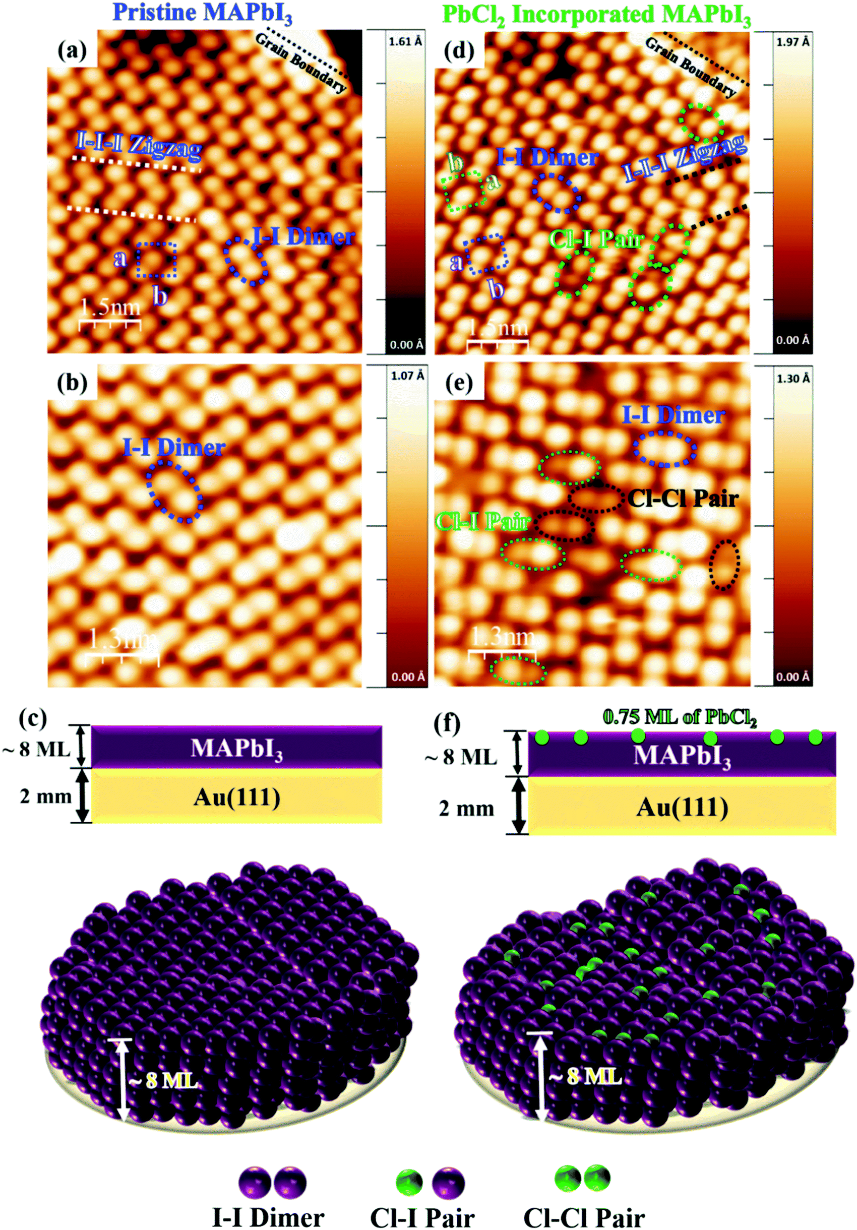 | ||
| Fig. 1 LT-STM images of the surface of the pristine MAPbI3 perovskite thin film and the 0.75 ML of PbCl2 incorporated MAPbI3 perovskite thin film deposited on Au(111). (a and b) I–I dimer (blue dashed ellipses) and I–I–I zigzag structures (white dashed lines) on the pristine MAPbI3 thin film surface (scan area = 14 × 14 nm2; sample bias voltage = −2.5 V; tunnelling current = 50 pA) with the unit cell (blue dashed square). (c) Atomic model configuration of pristine MAPbI3 on Au(111). (d and e) I–I dimers and Cl incorporated Cl–I pair structures (green dashed ellipses) in the centre, close to the grain boundary (green dashed line), inside a grain (scan area = 14.5 × 14.5 nm2; sample bias voltage = −2.5 V; tunnelling current = 50 pA) with the unit cell (green dashed square) and Cl–Cl pair (black dashed ellipses). (f) Atomic model configuration of 0.75 ML of PbCl2 incorporated MAPbI3 on Au(111). | ||
We prepared a total of 7 samples and the results were reproducible for the 0.75 ML of PbCl2 on MAPbI3. Fig. 2 shows the histogram of the apparent height distribution observed at the surface of the MAPbI3 perovskite after Cl ion incorporation (0.75 ML of PbCl2). The determination of the surface concentration of Cl in MAPbI3 was carefully analysed because the surface inhomogeneity of Cl in MAPbI3 was previously reported.51 The protrusion statistics were obtained from 12 STM images acquired on different macroscopic areas of the same sample and are consistent from sample to sample (7 samples in total). The comparison of the pristine and Cl incorporated dimer and zigzag structures is shown in Fig. 3a–l. The distribution of the STM apparent height values for the protrusions observed in these STM images (approximately 900 protrusions) is illustrated by the histogram shown in Fig. 2, and reveals that the average STM apparent height of dark protrusions observed in the STM images is about 0.5 ± 0.2 Å lower than the neighbouring iodine ions (Fig. 3d, e and j, k).
 | ||
| Fig. 2 Histogram of the apparent height distribution of I and Cl anions. The surface concentration in MAPbI3 is 14.8 ± 0.6%, which was obtained from the statistical analyses on the basis of 900 data points. | ||
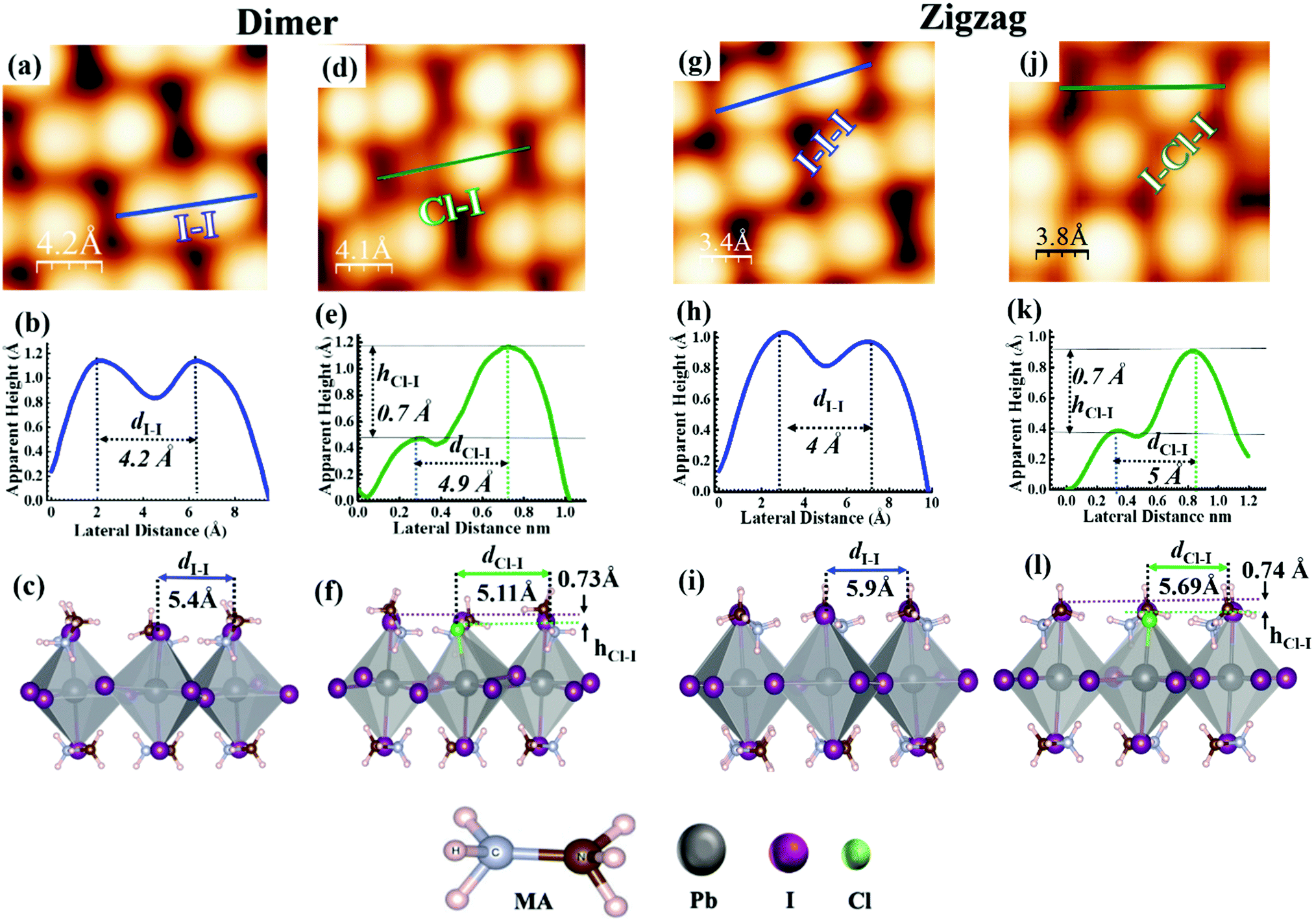 | ||
| Fig. 3 STM images of pristine and Cl incorporation in a dimer and zigzag structure of MAPbI3. (a) High-resolution STM image showing an I–I dimer structure (scan area = 18 × 18 Å2; sample bias voltage = −2.50 V, tunneling current = 20 pA). (b) Height profile and bond length of the observed I–I dimer in (a). (c) DFT simulated height profile and bond length for the I–I dimer in (a). (d) High-resolution STM image showing one Cl ion that forms a pair with one I ion in a dimer structure (scan area = 18 × 18 Å2; sample bias voltage = −2.50 V, tunneling current = 20 pA). (e) Height profile and bond length of the observed Cl–I pair in (d). (f) DFT simulated height profile and bond length for the Cl–I pair in (d). (g) High-resolution STM image showing I–I–I that forms a zigzag structure (scan area = 15 × 15 Å2; sample bias voltage = −2.50 V, tunneling current = 20 pA). (h) Height profile and bond length of the observed I–I zigzag structure in (g). (i) DFT simulated height profile and bond length of the observed I–I zigzag structure in (g). (j) High-resolution STM image showing one Cl ion that forms a pair with one I ion in a zigzag structure (scan area = 15 × 15 Å2; sample bias voltage = −2.50 V, tunneling current = 20 pA). (k) Height profile and bond length of the observed Cl–I zigzag structure in (j). (l) DFT simulated height profile and bond length of the observed Cl–I zigzag structure (j). Color code for (c), (f), (i) and (l): Pb (dark gray), I (purple), Cl (green), N (brown), C (ice blue), H (light pink). | ||
To unravel the origin of the dark protrusions observed in the STM images of MAPbI3 after PbCl2 deposition, we performed DFT calculations by using the Vienna ab initio simulation package (VASP) (see the Methods section). By tentatively assigning the dark protrusions to Cl ions, we obtained simulated STM images of the Cl-incorporated MAPbI3 surfaces. The simulated images reproduce accurately the dimer and zigzag structures observed experimentally for the MAPbI3 surface (Fig S3). Our calculations also reproduce the lowering of the apparent height due to Cl incorporation, which agrees with the experimental STM results (Fig. 3d and j). The incorporated Cl ions in the simulated models were found to be 0.73–0.74 Å (Fig. 3f and l) lower than their neighbouring iodine ions, which agrees well with the experimental value of ∼0.7 Å in Fig. 3e and k and the average value of 0.5 ± 0.2 Å based on the statistical analyses in Fig. 2. Also, we found that the experimental bond lengths (dCl-I) of the Cl–I pairs (∼4.9 and ∼5.0 Å) in the dimer and zigzag structures (Fig. 3e and k) were 5.11 and 5.69 Å, respectively (Fig. 3f and l and Fig. S3b and e, ESI†), which were also in line with the simulated results. Based on the experimental STM data in combination with the DFT calculations and XPS measurement results (Fig. S4–S6, ESI†), we can safely conclude that the dark protrusions in our STM images of the MAPbI3 surface after 0.5 ML and 0.75 ML of PbCl2 deposition are Cl ions that substitute iodine ions on the perovskite film surface. For simplicity, in the following discussions, we denote Cl-incorporated MAPbI3 as MAPb (I1−xClx)3 with x representing the concentration of Cl ions at the surface.
Based on our STM images, on the surface of MAPb(I1−xClx)3, most Cl ions were observed in the regions close to the grain boundaries and only a few in the center of the grains (Fig. 1d, e and Fig. S2b, c, ESI†). The substitution of I ions by Cl ions was observed for both the dimer and zigzag structures (Fig. 3d and j). The majority of incorporated Cl ions were found to form Cl–I pairs with neighbouring I ions (see the dashed circles in Fig. 1d and e). Note that DFT calculations suggest that the dimer structures associated with both the pristine and Cl-incorporated surfaces are more stable than the zigzag ones by about 0.030 eV, in good agreement with the energy difference of 0.034 eV reported in a previous study. 34 In addition, the experimental STM images (Fig. 1e) also show a few incorporated Cl ions bonding together to form the Cl–Cl pairs. The possibility of the appearance of these Cl–Cl pairs was also confirmed by DFT calculations, and the simulated STM images (Fig. S7, ESI†) reproducing well the Cl–Cl configurations observed in the STM experiments.
Fig. 4 shows several configurations for adjacent (Fig. 4a and d) and non-adjacent Cl–I pairs (Fig. 4g) in the dimer structure observed in STM experiments. DFT calculations verified the possibilities of these configurations (Fig. 4b, c, e, f, h and i) as well as predicted several other possible configurations for the adjacent and non-adjacent Cl–I pairs in the dimer and zigzag structures, as shown in Fig. S7 and S8 (ESI†). Note that these configurations in the dimer (Fig. 4 and Fig. S7, ESI†) or zigzag (Fig. S8, ESI†) structures have rather close total energies, which rationalizes the variety of configurations for two Cl–I pairs observed in Fig. 4.
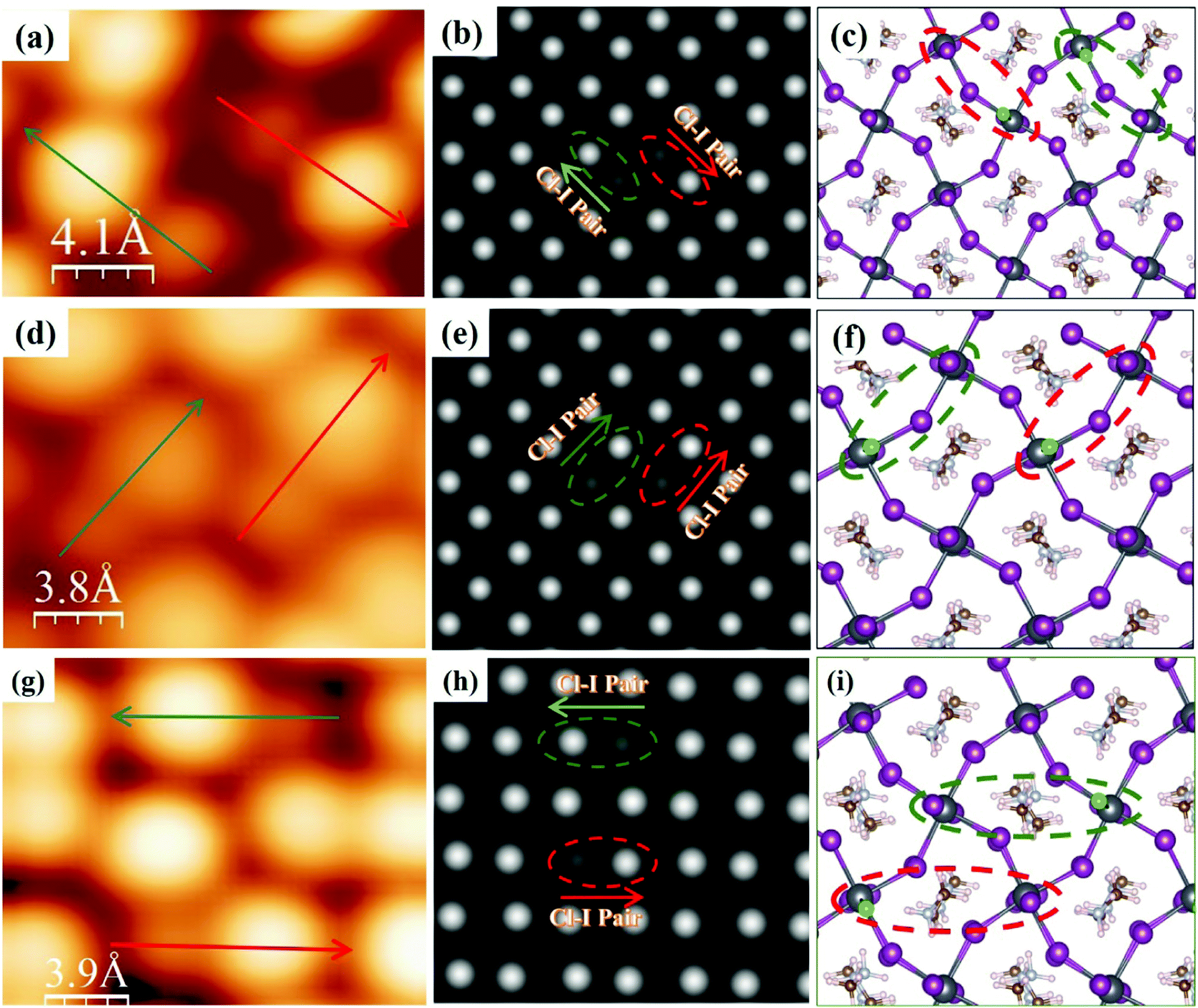 | ||
| Fig. 4 STM images of different configurations of Cl–I pairs in the dimer structure. (a) High-resolution STM images of two adjacent Cl–I pairs with opposite directions; arrows indicate the direction from Cl to I ions in the dimer (scan area = 1 × 1.6 nm2; sample bias voltage = −2.50 V, tunneling current = 30 pA). (b and c) Simulated STM image and atomic model for the two Cl–I pairs observed in (a). (d) High-resolution STM image of two adjacent Cl–I pairs showing the same parallel orientation; arrows indicate the direction from Cl to I ion in the dimer (scan area = 1.4 × 1.8 nm2; sample bias voltage = −2.50 V, tunneling current = 30 pA) in two parallel dimers in the small grain in Fig. 1(d and e). (e and f) Simulated STM image and atomic model for the two Cl–I pairs observed in (d). (g) High-resolution STM image of two non-adjacent Cl–I pairs with opposite directions (scan area = 1.7 × 2 nm2; sample bias voltage = −2.50 V, tunneling current = 30 pA) (h and i) simulated STM image and atomic model for the two Cl–I pairs observed in (g). Color code for (c), (f), and (i): Pb (dark gray), I (purple), Cl (green), N (brown), C (ice blue), H (light pink). | ||
We increased the deposition time of PbCl2 to 12 min to achieve more Cl ion incorporation in the dimer and zigzag structures, but we observed that the MAPbI3 film was completely covered by the 1.5 ML of PbCl2 (Fig. 5). Note that by XPS measurements (Fig. S6, ESI†) on the fully covered MAPbI3 surface by PbCl2, we observed a higher Cl concentration in comparison with the samples after a shorter time of PbCl2 deposition. Considering the fact that the 1 min deposition of PbCl2 did not lead to the surface incorporation of Cl ions in the MAPbI3 film, we deduced that the stable Cl surface incorporation should correspond to those samples after 0.5 ML and 0.75 ML deposition of PbCl2. According to the histogram shown in Fig. 2, the [Cl]:([Cl] + [I]) concentration of 14.8 ± 0.6% was extracted for the Cl incorporated MAPbI3 (i.e., MAPb(I0.85Cl0.15)3). However, according to the XPS results (Fig. S5, ESI†), an incorporated Cl concentration of 40% was determined, which significantly differs from the concentration extracted from the STM histogram analyses (Fig. 2). This is possibly because XPS measurements not only probe Cl ions mixed in the top surface layer but also those in sub-surface layers.
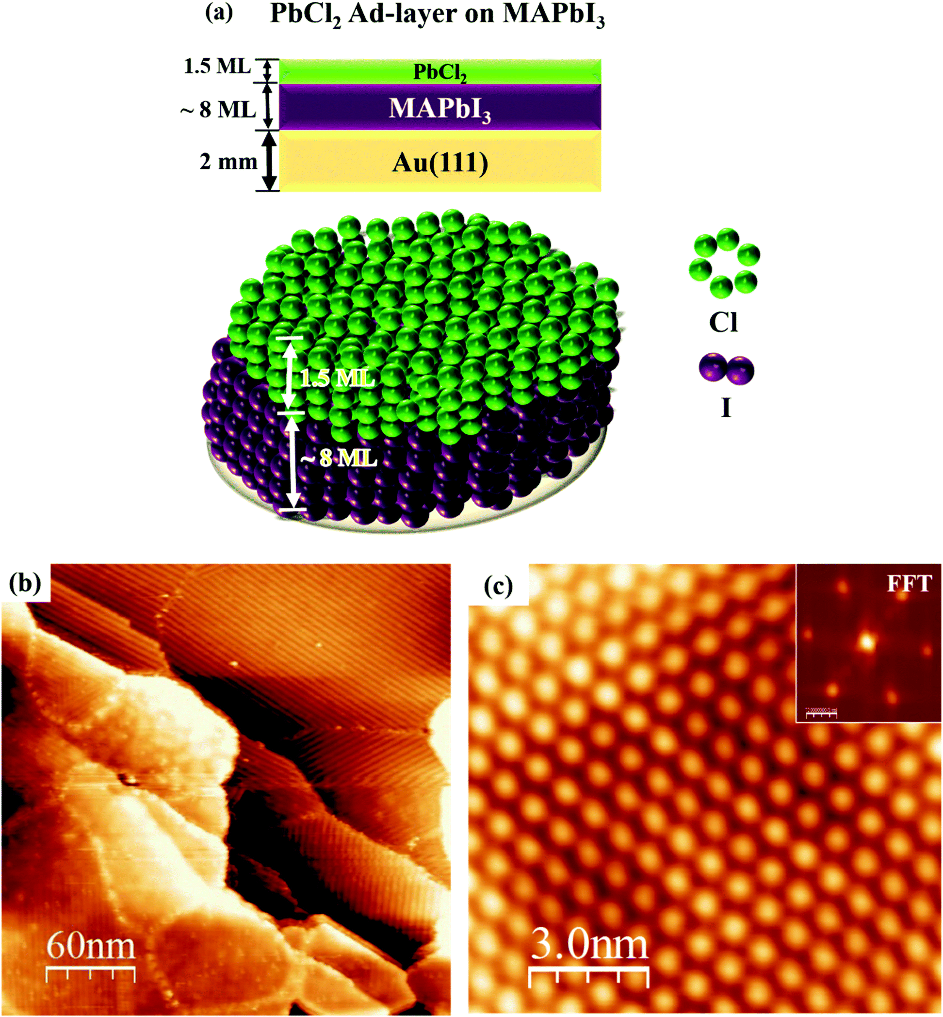 | ||
| Fig. 5 Atomic model and STM high-resolution images of the MAPbI3 thin film after 1.5 ML of PbCl2 deposition. (a) Atomic model configuration of 1.5 ML PbCl2 ad-layer on MAPbI3. (b) Large area STM topography image of PbCl2 fully covering the MAPbI3 thin film (scan area = 300 × 300 nm2, sample bias voltage = −2.50 V, tunnelling current = 400 pA). (c) High-resolution STM image of the PbCl2 surface structure located in the centre of a grain. (Scan area = 13 × 15 nm2) (sample bias voltage = −2.50 V, tunnelling current = 400 pA). Inset shows the fast Fourier transform (FFT) image indicating the hexagonal structure of PbCl2. | ||
We further investigated the influence of the incorporated Cl ions on the electronic properties of MAPbI3 films by UPS and IPES measurements (Fig. 6a). Based on the UPS and IPES measurement results, the bandgap of the pristine MAPbI3 film was determined to be 1.13 eV. Note that this bandgap value is substantially lower than the previously reported bandgap of 1.7 eV measured on relatively thick MAPbI3 films,63 which is possibly a result of the substrate effect because of the ultrathin film MAPbI3 samples used in this study. After Cl incorporation with 0.75 ML deposition of PbCl2, the bandgap increased to 1.62 eV (0.49 eV larger than that of the pristine MAPbI3 film), suggesting that the incorporation of Cl ions can effectively tune the electronic properties of MAPbI3.24,52 Our STM and XPS results suggest that Cl ions are not only incorporated in the top layer but also in the sub-surface layers. To determine the main factor that causes the surface bandgap change, we calculated the bandgaps (Fig. 6b) of the MAPbI3 surface models with Cl ions being only incorporated in the top one, top two, and top four layers as a function of the incorporation ratio (assuming the same Cl concentration for all the relevant layers when Cl ions are incorporated into multiple layers), as shown in Fig. 6b. It can be seen that there are no substantial bandgap changes when Cl ions are only mixed into the top layer, being the same as that for Cl-incorporated MAPbBr3.30 However, when Cl ions are contained in the sub-surface layers, the bandgap increases fast with the increasing chlorine incorporation concentration. This trend is even clearer in the case of Cl ions being incorporated in the top four layers. This indicates that the bandgap enlargement observed in the experiment is mainly a synergic effect of the Cl incorporation in the multiple surface layers (or in other words, more a multi-layer film effect rather than a surface effect). From Fig. 6b, we can realize that Cl ions are incorporated in at least the top four layers of the surface model consisting of a total of 8 ML of the perovskite lattice structure (here, we consider the MAI layer as a layer and the PbI2 layer as another layer), as only under this situation the increase of the bandgap (∼0.49 eV) determined by UPS/IPES measurements can be explained qualitatively. We further calculated the density of states (DOS) for the pristine MAPbI3 surface and that with Cl ions incorporated in the top four layers at the concentration of 18.75%, being quite close to the surface Cl ratio of (14.8% ± 0.6%) determined by STM. The comparison of DOS in Fig. 6c also confirmed that incorporated Cl ions would enlarge the bandgap of MAPbI3 by 0.2 eV as a result of the upward and downward shift of the valence and conduction band edges, respectively (Fig. 6c), which is consistent with the experimental observation (Fig. 6a). In addition, the perovskite surface bandgap combined with the analyses of energy level alignments (Fig. S9, ESI†) plays a key role in PSCs53 (Section S1, ESI†).
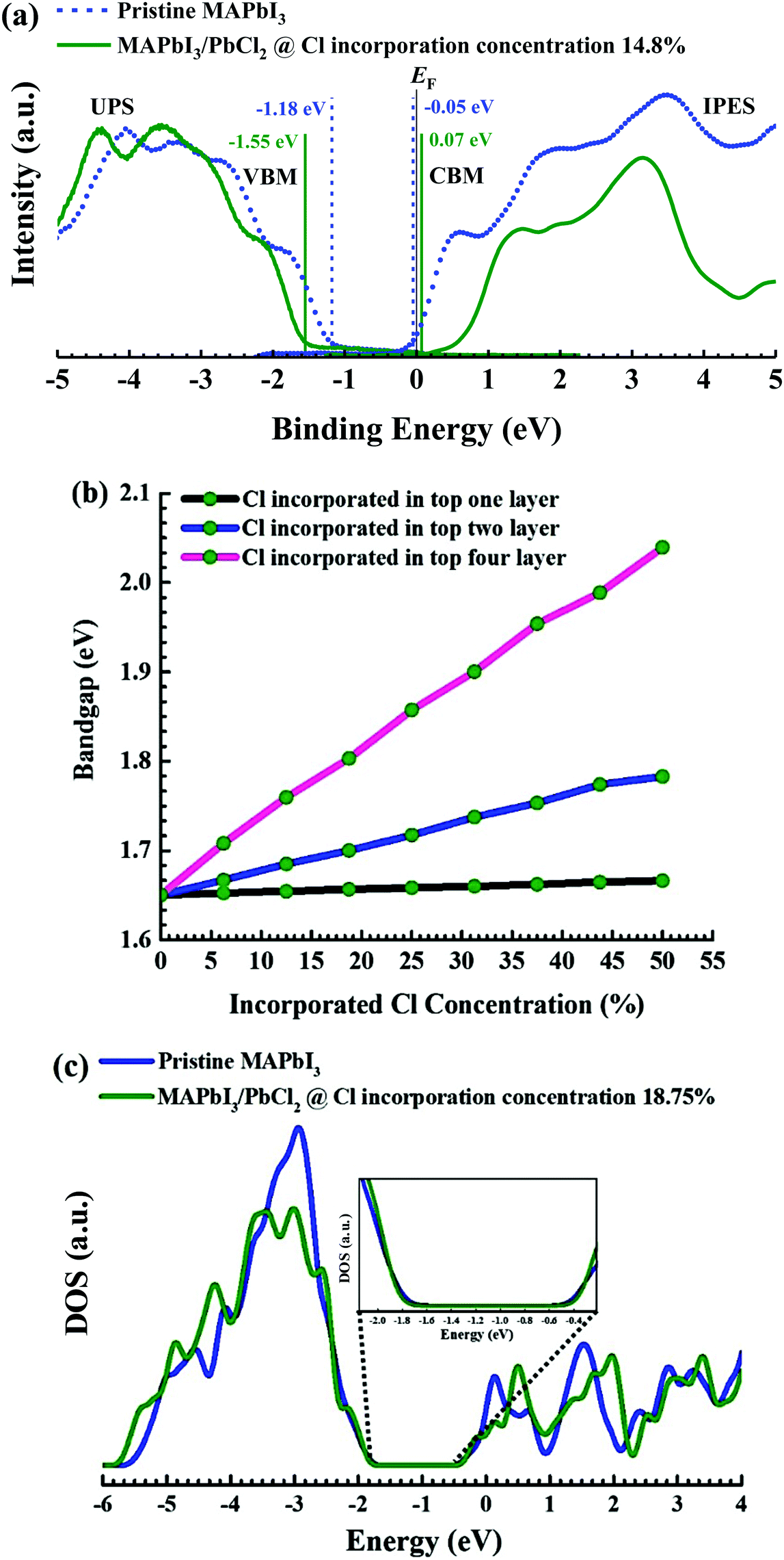 | ||
| Fig. 6 Experimental and DFT calculated bandgap of pristine and Cl incorporated MAPbI3. (a) Experimental ultraviolet and inverse photoemission spectroscopy (UPS-IPES) spectra of the pristine (dashed blue curves) and Cl-incorporated (solid green curves) MAPbI3 surfaces. (b) Calculated bandgaps of the MAPbI3 surface model with Cl ions only being incorporated in the dimer structure into the top one (black), top two (blue), and top four layers (pink) as a function of the incorporation ratio. (c) Calculated DOS of the pristine and Cl-incorporated MAPbI3 surfaces. For the latter, Cl ions are incorporated into the top four layers of the model at the [Cl]:([Cl] + [I]) concentration of 18.75%. VBM = Valence band maximum, CBM = conduction band minimum. A wider bandgap was observed after Cl incorporation. | ||
Previous studies have suggested that Cl incorporation can increase the stability of perovskite materials and solar cell devices.30,54 Therefore, to unravel the origin of the enhanced stability of the Cl-incorporated MAPbI3 surface, we evaluated the changes in the decomposition energy (see the Methods section) of the MAPb(I1−xClx)3 film for different Cl incorporation concentrations through DFT calculations. Here, we consider two different incorporation modes: (1) Cl ions only being incorporated in the top layer of the surface, corresponding to Fig. 7a; (2) Cl ions only being incorporated in the second layer, corresponding to Fig. 7b. It is noticed that upon increasing the incorporated Cl amount, the decomposition energy profiles for both incorporation modes show firstly an increase, and then a decrease. The increase of the decomposition energy is related to the stronger bond strength of Cl–Pb compared to that of I–Pb.55,56 This bond strength originates from the radius of Cl− being smaller than that of I−, causing a shorter bond length and in turn a stronger electrostatic interaction between bonded Cl− and Pb2+ than that between bonded I− and Pb2+. However, the incorporation of the smaller Cl− ion in the inorganic lattice of MAPbI3 also induces the strain, which in turn pushes up the total energy of the system. At low Cl concentrations (i.e., below 18.75%), the influence of the strain on the total energy of the system is not predominant. But when the Cl concentration exceeds a threshold, the strain overrides the benefit of the stronger Cl–Pb bond, leading to the reduction in the decomposition energy. An increase of the decomposition energy with low concentrations of Cl incorporation suggests a higher stability of the MAPbI3 film concerning external stimuli such as temperature or X-ray beams.57 Also, it is found that the maximum increase of the decomposition energy for the incorporation in the second layer (Fig. 7b) is 0.08 eV larger than that for the incorporation in the top layer (Fig. 7a), which indicates that Cl ions mixed into the sub-surface layers play a more significant role in stabilizing the MAPbI3 surface than those in the top layer alone.
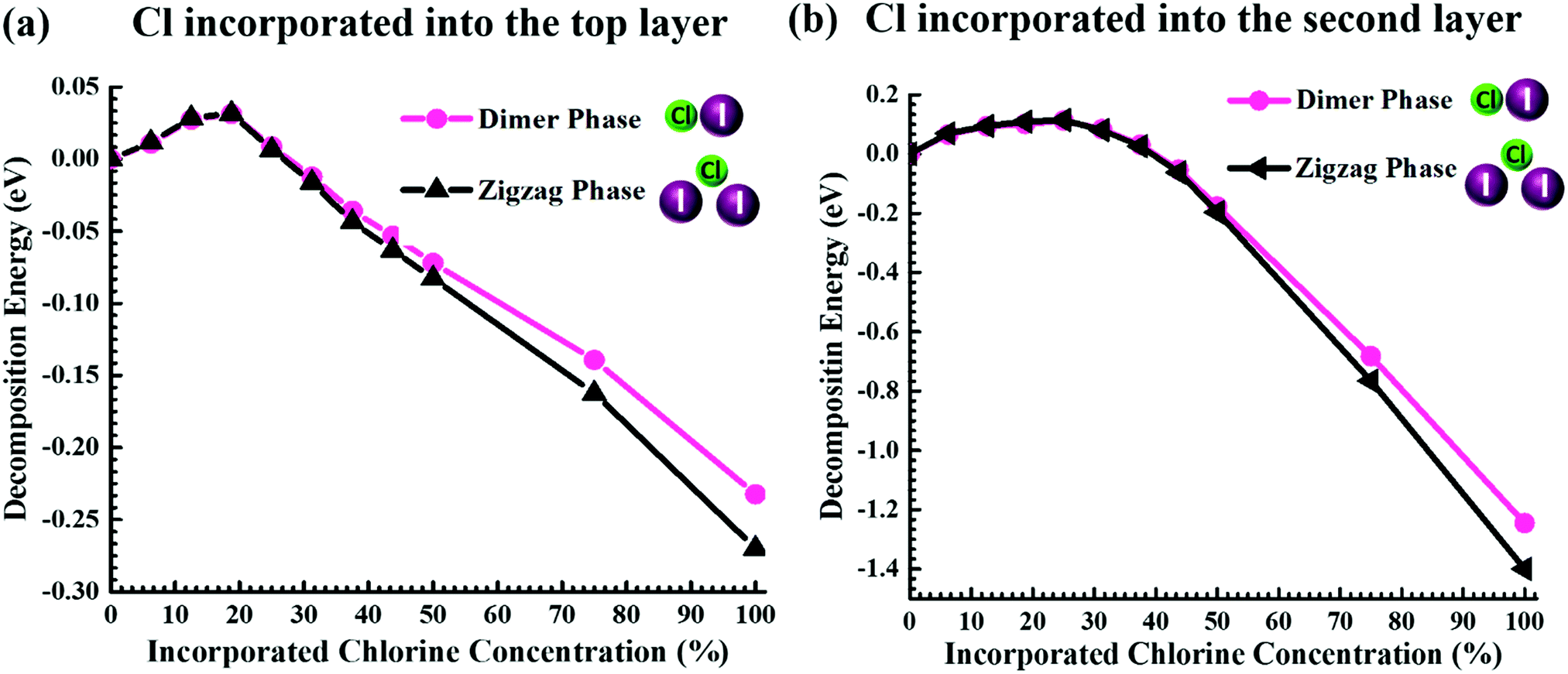 | ||
| Fig. 7 The decomposition energy difference between the pristine and Cl-incorporated MAPbI3 surface determined by DFT calculations (see the Methods section): (a) Cl ions only incorporated in the top layer, and (b) Cl ions only incorporated in the second layer. | ||
In Fig. 7b, the predicted optimal incorporation concentration of Cl into the second layer is 25%, being noticeably higher than that of the top layer (18.75%), which is consistent with our XPS measurements showing that the concentration in the sub-surface layers is higher than that in the top layer. These results also suggest that the Cl− ions in the top-most surface layer can diffuse into the subsurface layers of the MAPbI3 ultra-thin film. We can also understand this experimental finding from the viewpoint of energy according to Fig. 7. From eqn (3) in the Methods section, we can know that at a fixed incorporated chlorine concentration, the higher decomposition energy corresponds to the lower total energy of MAPb(I1−xClx)3. It can be seen from Fig. 7 that when the incorporated concentration is less than ∼40%, the total energy of MAPb(I1−xClx)3 with the incorporation in the second layer is lower than that with the incorporation in the top layer, indicating that Cl ions prefer to stay in the sub-surface layers. This finding is consistent with the experimental observation that the incorporated Cl concentration in the sub-surface layers is higher than that in the top layer. Moreover, it is found that the decomposition energies within the positive range of both the dimer and zigzag structures differ negligibly, which corroborates the experimental observation of Cl ions incorporated in the surface structure with the dimer and zigzag structures simultaneously. Last but not least, when the incorporated [Cl]:([Cl] + [I]) concentration is higher than ∼25% for incorporation in the top layer and higher than ∼40% for incorporation in the second layer, the decomposition energy of MAPb(I1−xClx)3 becomes negative, meaning that MAPb(I1−xClx)3 cannot exist stably, which determines in principle that the incorporated concentration for stable MAPb(I1−xClx)3 samples will not exceed 25% in the top layer and 40% in the second layer. These predicted upper limits are consistent with our experimental results showing the incorporated Cl concentration of 14.8 ± 0.6% in the top layer and 40% on average in several other sub-surface layers.
To further understand the influence of Cl ions on the stability of Cl-incorporated MAPbI3 surfaces, we also calculated the surface energies of the pristine MAPbI3 surface and that with one I− being substituted by Cl− in the top layer (see Methods section), which are summarized in Table 1. Note that the incorporation of one Cl atom in the MAPbI3 surface leads to a surface energy decrease of 76 meV and 71 meV for the dimer and zigzag structures, respectively (Table 1), which can also explain the stabilization effect of Cl ions on the MAPbI3 surfaces. Also, we performed molecular dynamics (MD) simulations of pristine and Cl-incorporated MAPbI3 surfaces with the dimer structure to examine the impact of Cl ions on the vibration of I and Pb atoms in the top and second layers, by calculating the average moving distances for Pb and I atoms during the 1 ps MD simulation, which are shown in Table 2.
| Perovskite | Dimer | Zigzag |
|---|---|---|
| MAPbI3 | 6.354 | 6.385 |
| MAPb(I1−xClx)3 | 6.278 | 6.314 |
| MAPbI3 | MAPb(I1−xClx)3 (one Cl atom in the first layer) | MAPb(I1−xClx)3 (one Cl atom in the second layer) | |
|---|---|---|---|
| d I1 (Å) | 2.477 | 2.475 | 2.428 |
| d I2 (Å) | 2.605 | 2.481 | 2.336 |
| d Pb (Å) | 2.009 | 2.008 | 1.934 |
These results allow us to analyse the stabilization effect of incorporated Cl ions on the MAPbI3 surface from the viewpoint of kinetics. It is noticed that the incorporation of one Cl ion in the top or second layer suppresses the vibration of Pb and I ions in the first and second layer of the surface (Fig. S3, ESI†). The weaker vibration of the inorganic lattice will to some extent suppress the diffusion of some intrinsic defects, such as iodine vacancy and interstitial defects, which contributes to the improved stability of MAPb(I1−xClx)3 surfaces. It is interesting to point out that the Cl ion incorporated in the second layer generates a more obvious impact on lowering the vibration strength of Pb and I atoms than the Cl atom in the top layer, being consistent with the analyses for the decomposition energy in Fig. 7. In conclusion, our DFT calculations verify that the incorporation of Cl ions indeed stabilizes the MAPbI3 surface from the viewpoints of both thermodynamics and kinetics.
Conclusions
In this work, we determined the atomic-scale structure of the Cl incorporated MAPbI3 surfaces. It is found that Cl ions are incorporated in both the MAPbI3 surface and sub-surface layers. Most of the Cl ions incorporated on the surface were found close to the grain boundaries, but some are also found at the centre of the grains for both the dimer and zigzag structures of MAPbI3. Additionally, our XPS measurement results confirm that Cl ions are not present at the surface of MAPbI3 with a short time of PbCl2 deposition, and with a sufficiently long time of PbCl2 deposition (e.g., 12 min), the MAPbI3 surface is fully covered by PbCl2. Moreover, the surface bandgap of the ultrathin film of MAPbI3 is found to be increased by approximately 0.49 eV from 1.13 eV to 1.62 eV when 0.75 ML of PbCl2 is deposited onto the MAPbI3 surface. DFT calculations also predict the bandgap increase observed in the experiment at a similar Cl concentration, and suggests that the incorporation of Cl in the subsurface layers is found to have a stronger impact on the bandgap with respect to Cl ion substitution at only the topmost surface layer. Furthermore, DFT calculations and MD calculations reveal a strong increase of the perovskite stability for low Cl concentrations (below 18.75%). The increase of stability is even more pronounced when substituting the Cl ions in the subsurface layer with respect to the top surface layer. The perovskite material was found to be stable both thermodynamically and kinetically. Our findings provide insights into further understanding of the perovskite material and a more rational design of future high stability perovskite solar cells.Methods
A. Surface characterization
Cl incorporated MAPbI3 ultra-thin films on clean Au(111) were studied in an ultrahigh vacuum (UHV) system by STM (base pressure <2 × 10⁻¹⁰ Torr). Au(111) single crystals were used as the substrates following our previous study.32 First, the Au(111) substrate was cleaned under UHV conditions by three cycles of Ne+ sputtering (7.5 × 10⁻⁵ Torr; 60 min) followed by annealing at 773 K for 20 min. MAPbI3 perovskite films were prepared by co-evaporating PbI2 and MAI precursors at the temperatures of 516 K and 395 K, respectively, for 3 min. During the co-deposition of PbI2 and MAI, the Au(111) substrate was kept at a temperature of 132 K to ensure a high sticking coefficient of MAI. After evaporation, the sample was annealed at room temperature for 3 h. This protocol leads to MAPbI3 films with a thickness of ~4–5 nm and with typical grain sizes ranging from 8 nm to 15 nm (Fig. S1a, ESI†). Cl incorporated MAPbI3 samples were obtained by evaporating PbCl2 for a certain duration of time (namely, 1 min, 4 min, 6 min, and 12 min) on top of the pristine MAPbI3 film on the Au(111) substrate. The halide ion exchange reaction takes place according to the following equation: | (1) |
The samples were in situ transferred onto a low-temperature scanning tunneling microscope (LT-STM, Scienta Omicron GmbH) for measurements. The STM measurements were performed at 77 K using Pt/Ir STM tips and with the bias voltage applied to the sample. After the STM measurements, the samples were in situ transferred to the analysis chamber (the base pressure of ∼2 × 10⁻¹⁰ Torr) equipped with a hemispherical electron energy analyzer (EA 125, Scienta Omicron GmbH), a He discharge lamp (HIS 13, Scienta Omicron GmbH; He-Iα = 21.22 eV) with an energy resolution of ∼0.15 eV for UPS measurements, and a dual-anode (Al-Kα = 1486.6 eV and Mg-Kα = 1253.6 eV) non-monochromatic X-ray source (DAR 400, Scienta Omicron GmbH) with an energy resolution of ∼0.8 eV for XPS measurements. IPES (LE-1, ALS Technology Co., Ltd)58 measurements were performed in a separate vacuum system, and the sample transfer was conducted with the aid of a custom-designed vacuum suitcase (Ferrovac GmbH), which ensures no ambient exposure during sample transfer. For the quantitative analyses of the peak positions, line widths, and relative areas of the Pb 4f, I 3d, C 1s, N 1s, and Cl 2p XPS data, the raw XPS spectra were fitted with Gaussian–Lorentzian functions using the CASA XPS software.
B. Density functional theory
Density functional theory (DFT) calculations were performed by using the VASP code59 with the standard frozen-core projector augmented-wave (PAW) method60 and the Perdew–Burke–Ernzerhof (PBE) exchange–correlation functional.61 For the plane-waves, a cutoff of 450 eV was employed. The nonlocal van der Waals interactions were considered by using the Becke–Jonson damping DFT-D3 method.62 No spin-orbital coupling (SOC) was considered in this work. The lattice parameters (a = 8.84 Å, b = 8.47 Å, and c = 12.65 Å) of the MAPbI3 unit cell in the orthorhombic phase were achieved through structural relaxation by adopting a 4 × 4 × 4 Monkhorst–Pack grid. The MAPbI3 (010) surfaces were modeled by using the 2 × 2 slabs with a vacuum thickness of 20 Å. Each surface model contained eight atomic layers, among which the bottom four layers were always kept fixed at their bulk positions and the other layers were fully relaxed until the atomic forces converged within 0.01 eV Å−1 (Fig. S3, ESI†). For all calculations involving the surfaces, the Brillouin zone was sampled at the sole Γ-point. From the electronic ground state structure, STM images were obtained by using the p4vasp code. All MD simulations were carried out by using the canonical (NVT) ensemble with the temperature being controlled at 300 K through the Nosé–Hoover thermostat. The surface energies (Es) reported in Table 1 are calculated by using the following equation:| Es = Eslab − Ebulk, | (2) |
To evaluate the stability of the Cl incorporated MAPbI3 surface, we consider the following reaction:30
 | (3) |
 | (4) |
Author contributions
Y. B. Q. conceived the idea, designed the experiments, and supervised the project. A. J., J. H., C. S., R. O., and L. K. O. performed the STM experiments and data analyses. A. J. and L. K. O. performed the XPS, UPS, and IPES measurements and analyses. Z. G. and W. J. performed the DFT calculations. L. Q. and G. T. provided valuable suggestions. All authors contributed to writing the paper. A. J. and Z. G. contributed equally to this work.Conflicts of interest
The authors declare no competing financial interest.Acknowledgements
This work was supported by funding from the Energy Materials and Surface Sciences Unit of the Okinawa Institute of Science and Technology Graduate University, the OIST R&D Cluster Research Program, the OIST Proof of Concept (POC) Program, the JSPS KAKENHI Grant Number JP18K05266, and JST A-STEP Grant Number JPMJTM20HS, Japan. W. Y. acknowledges the funding support from the National Natural Science Foundation of China (Grant No. 11974257 and 11674237).References
- A. Kojima, K. Teshima, Y. Shirai and T. Miyasaka, Organometal halide perovskites as visible-light sensitizers for photovoltaic cells, J. Am. Chem. Soc., 2009, 131, 6050 CrossRef CAS PubMed.
- Best Research-Cell Efficiencies, National Renewable Energy Laboratory (NREL) https://www.nrel.gov/pv/assets/pdfs/best-research-cell-efficiencies.20200104.pdf (accessed June 6th, 2021).
- N. Li, X. Niu, Q. Chen and H. Zhou, Towards commercialization: The operational stability of perovskite solar cells, Chem. Soc. Rev., 2020, 49, 8235–8286 RSC.
- M. Saliba, Polyelemental, multicomponent perovskite semiconductor libraries through combinatorial screening, Adv. Energy Mater., 2019, 9(25), 1803754 CrossRef.
- L. Qiu, S. He, L. K. Ono and Y. B. Qi, Progress of surface science studies on ABX3-based metal halide perovskite solar cells, Adv. Energy Mater., 2020, 1902726 CrossRef CAS.
- N. J. Jeon, J. H. Noh, W. S. Yang, Y. C. Kim, S. Ryu, J. Seo and S. I. Seok, Compositional engineering of perovskite materials for high-performance solar cells, Nature, 2015, 517(7535), 476–480 CrossRef CAS PubMed.
- G. Tong, X. Lan, Z. Song, G. Li, H. Li, L. Yu, J. Xu, Y. Jiang, Y. Sheng, Y. Shi and K. Chen, Surface-activation modified perovskite crystallization for improving photovoltaic performance, Mater. Today Energy, 2017, 5, 173–180 CrossRef.
- G. Tong, D.-Y. Son, L. K. Ono, Y. Liu, Y. Hu, H. Zhang, A. Jamshaid, L. Qiu, Z. Liu and Y. B. Qi, Scalable fabrication of >90 cm2 perovskite solar modules with >1000 h operational stability based on the intermediate phase strategy, Adv. Energy Mater., 2020, 10, 2003712 Search PubMed.
- K. Odysseas Kosmatos, L. Theofylaktos, E. Giannakaki, D. Deligiannis, M. Konstantakou and T. Stergiopoulos, Methylammonium chloride: A key additive for highly efficient, stable, and up-scalable perovskite solar cells, Energy Environ. Mater., 2019, 2(2), 79–92 CrossRef CAS.
- W. A. Dunlap-Shohl, Y. Zhou, N. P. Padture and D. B. Mitzi, Synthetic approaches for halide perovskite thin films, Chem. Rev., 2019, 119(5), 3193–3295 CrossRef CAS PubMed.
- L. K. Ono, E. J. Juarez-Perez and Y. B. Qi, Progress on perovskite materials and solar cells with mixed cations and halide anions, ACS Appl. Mater. Interfaces, 2017, 9(36), 30197–30246 CrossRef CAS PubMed.
- V. L. Pool, A. Gold-Parker, M. D. McGehee and M. F. Toney, Chlorine in PbCl2-derived hybrid-perovskite solar absorbers, Chem. Mater., 2015, 27(21), 7240–7243 CrossRef CAS.
- M. Kim, G.-H. Kim, T. K. Lee, I. W. Choi, H. W. Choi, Y. Jo, Y. J. Yoon, J. W. Kim, J. Lee, D. Huh, H. Lee, S. K. Kwak, J. Y. Kim and D. S. Kim, Methylammonium chloride induces intermediate phase stabilization for efficient perovskite solar cells, Joule, 2019, 3(9), 2179–2192 CrossRef CAS.
- J. Xu, C. C. Boyd, Z. J. Yu, A. F. Palmstrom, D. J. Witter, B. W. Larson, R. M. France, J. Werner, S. P. Harvey, E. J. Wolf, W. Weigand, S. Manzoor, M. F. A. M. van Hest, J. J. Berry, J. M. Luther, Z. C. Holman and M. D. McGehee, Triple-halide wide-band gap perovskites with suppressed phase segregation for efficient tandems, Science, 2020, 367(6482), 1097–1104 CrossRef CAS PubMed.
- J.-W. Lee and N.-G. Park, Chemical approaches for stabilizing perovskite solar cells, Adv. Energy Mater., 2020, 10(1), 1903249 CrossRef CAS.
- C. Mu, J. Pan, S. Feng, Q. Li and D. Xu, Quantitative doping of chlorine in formamidinium lead trihalide (FAPbI3−xClx) for planar heterojunction perovskite solar cells, Adv. Energy Mater., 2017, 7(6), 1601297 CrossRef.
- K. Wang, Z. Jin, L. Liang, H. Bian, H. Wang, J. Feng, Q. Wang and S. Liu, Chlorine doping for black γ-CsPbI3 solar cells with stabilized efficiency beyond 16%, Nano Energy, 2019, 58, 175–182 CrossRef CAS.
- Z. Liu, L. K. Ono and Y. B. Qi, Additives in metal halide perovskite films and their applications in solar cells, J. Energy Chem., 2020, 46, 215–228 CrossRef.
- T.-W. Ng, C.-Y. Chan, M.-F. Lo, Z. Q. Guan and C.-S. Lee, Formation chemistry of perovskites with mixed iodide/chloride content and the implications on charge transport properties, J. Mater. Chem. A, 2015, 3(17), 9081–9085 RSC.
- M. Wang, B. Li, P. Siffalovic, L.-C. Chen, G. Cao and J. Tian, Monolayer-like hybrid halide perovskite films prepared by additive engineering without antisolvents for solar cells, J. Mater. Chem. A, 2018, 6(31), 15386–15394 RSC.
- M. Bouchard, J. Hilhorst, S. Pouget, F. Alam, M. Mendez, D. Djurado, D. Aldakov, T. Schülli and P. Reiss, Direct evidence of chlorine-induced preferential crystalline orientation in methylammonium lead iodide perovskites grown on TiO2, J. Am. Chem. Soc., 2017, 121(14), 7596–7602 Search PubMed.
- L. A. Muscarella, E. M. Hutter, S. Sanchez, C. D. Dieleman, T. J. Savenije, A. Hagfeldt, M. Saliba and B. Ehrler, Crystal orientation and grain size: Do they determine optoelectronic properties of MAPbI3 perovskite?, J. Phys. Chem. Lett., 2019, 10(20), 6010–6018 CrossRef CAS PubMed.
- K. Odysseas Kosmatos, L. Theofylaktos, E. Giannakaki, D. Deligiannis, M. Konstantakou and T. Stergiopoulos, Methylammonium chloride: A key additive for highly efficient, stable, and up-scalable perovskite solar cells, Energy Environ. Sci., 2019, 2(2), 79–92 CAS.
- Y. Li, W. Sun, W. Yan, S. Ye, H. Peng, Z. Liu, Z. Bian and C. Huang, High-performance planar solar cells based on CH3NH3PbI3−xClx perovskites with determined chlorine mole fraction, Adv. Funct. Mater., 2015, 25(30), 4867–4873 CrossRef CAS.
- H. Zhang, Q. Liao, X. Wang, K. Hu, J. Yao and H. Fu, Controlled substitution of chlorine for iodine in single-crystal nanofibers of mixed perovskite MAPbI3−xClx, Small, 2016, 12(28), 3780–3787 CrossRef CAS PubMed.
- S. Colella, E. Mosconi, P. Fedeli, A. Listorti, F. Gazza, F. Orlandi, P. Ferro, T. Besagni, A. Rizzo, G. Calestani, G. Gigli, F. De Angelis and R. Mosca, MAPbI3−xClx mixed halide perovskite for hybrid solar cells: The role of chloride as dopant on the transport and structural properties, Chem. Mater., 2013, 25(22), 4613–4618 CrossRef CAS.
- W.-J. Yin, H. Chen, T. Shi, S.-H. Wei and Y. Yan, Origin of high electronic quality in structurally disordered CH3NH3PbI3 and the passivation effect of Cl and O at grain boundaries, Adv. Electron. Mater., 2015, 1(6), 1500044 CrossRef.
- W. A. Dunlap-Shohl, Y. Zhou, N. P. Padture and D. B. Mitzi, Synthetic approaches for halide perovskite thin films, Chem. Rev., 2019, 119(5), 3193–3295 CrossRef CAS PubMed.
- J. Hieulle, S. Luo, D.-Y. Son, A. Jamshaid, C. Stecker, Z. Liu, G. Na, D. Yang, R. Ohmann, L. K. Ono, L. Zhang and Y. B. Qi, Imaging of the atomic structure of all-inorganic halide perovskites, J. Phys. Chem. Lett., 2020, 11(3), 818–823 CrossRef CAS PubMed.
- J. Hieulle, X. Wang, C. Stecker, D.-Y. Son, L. Qiu, R. Ohmann, L. K. Ono, A. Mugarza, Y. Yan and Y. B. Qi, Unraveling the impact of halide mixing on perovskite stability, J. Am. Chem. Soc., 2019, 141(8), 3515–3523 CrossRef CAS PubMed.
- C. Stecker, K. Liu, J. Hieulle, R. Ohmann, Z. Liu, L. K. Ono, G. Wang and Y. B. Qi, Surface defect dynamics in organic–inorganic hybrid perovskites: From mechanism to interfacial properties, ACS Nano, 2019, 13(10), 12127–12136 CrossRef CAS PubMed.
- R. Ohmann, L. K. Ono, H.-S. Kim, H. Lin, M. V. Lee, Y. Li, N.-G. Park and Y. B. Qi, Real-space imaging of the atomic structure of organic–inorganic perovskite, J. Am. Chem. Soc., 2015, 137(51), 16049–16054 CrossRef CAS PubMed.
- L. She, M. Liu, X. Li, Z. Cai and D. Zhong, Growth and interfacial structure of methylammonium lead iodide thin films on Au(111), Surf. Sci., 2017, 656, 17–23 CrossRef CAS.
- L. She, M. Liu and D. Zhong, Atomic structures of CH3NH3PbI3(001) surfaces, ACS Nano, 2016, 10(1), 1126–1131 CrossRef CAS PubMed.
- L. Cai, L. M. She, H. L. Qin, L. Xu and D. Y. Zhong, Monolayer methylammonium lead iodide films deposited on Au(111), Surf. Sci., 2018, 675, 78–82 CrossRef CAS.
- Z. Hu, Z. Lin, J. Su, J. Zhang, J. Chang and Y. Hao, A review on energy band-gap engineering for perovskite photovoltaics, Sol. RRL, 2019, 3(12), 1900304 CrossRef.
- W. Li, J. Tang, D. Casanova and O. V. Prezhdo, Time-domain ab initio analysis rationalizes the unusual temperature dependence of charge carrier relaxation in lead halide perovskite, ACS Energy Lett., 2018, 3(11), 2713–2720 CrossRef CAS.
- L. K. Ono, S. Liu and Y. B. Qi, Reducing detrimental defects for high-performance metal halide perovskite solar cells, Angew. Chem., Int. Ed., 2020, 59(17), 6676–6698 CrossRef CAS PubMed.
- F. Ambrosio, D. Meggiolaro, E. Mosconi and F. De Angelis, Charge localization and trapping at surfaces in lead-iodide perovskites: The role of polarons and defects, J. Mater. Chem. A, 2020, 8(14), 6882–6892 RSC.
- Q.-K. Wang, R.-B. Wang, P.-F. Shen, C. Li, Y.-Q. Li, L.-J. Liu, S. Duhm and J.-X. Tang, Energy level offsets at lead halide perovskite/organic hybrid interfaces and their impacts on charge separation, Adv. Mater. Interfaces, 2015, 2, 1400528 CrossRef.
- G. Nan, X. Zhang, M. Abdi Jalebi, Z. Andaji-Garmaroudi, S. Stranks, G. Lu and D. Beljonne, How methylammonium cations and chlorine dopants heal defects in lead iodide perovskites, Adv. Energy Mater., 2018, 8, 1702754 CrossRef.
- J. Wang, W. Li and W.-J. Yin, Passivating detrimental DX centers in CH3NH3PbI3 for reducing nonradiative recombination and elongating carrier lifetime, Adv. Mater., 2020, 32(6), 1906115 CrossRef CAS PubMed.
- L. K. Ono and Y. B. Qi, Surface and interface aspects of organometal halide perovskite materials and solar cells, J. Phys. Chem. Lett., 2016, 7(22), 4764–4794 CrossRef CAS PubMed.
- Z. Hawash, S. R. Raga, D.-Y. Son, L. K. Ono, N.-G. Park and Y. B. Qi, Interfacial modification of perovskite solar cells using an ultrathin MAI layer leads to enhanced energy level alignment, efficiencies, and reproducibility, J. Phys. Chem. Lett., 2017, 8(17), 3947–3953 CrossRef CAS PubMed.
- J. J. Yoo, G. Seo, M. R. Chua, T. G. Park, Y. Lu, F. Rotermund, Y.-K. Kim, C. S. Moon, N. J. Jeon, J.-P. Correa-Baena, V. Bulović, S. S. Shin, M. G. Bawendi and J. Seo, Efficient perovskite solar cells via improved carrier management, Nature, 2021, 590(7847), 587–593 CrossRef CAS PubMed.
- Z. Dai, S. K. Yadavalli, M. Chen, A. Abbaspourtamijani, Y. Qi and N. P. Padture, Interfacial toughening with self-assembled monolayers enhances perovskite solar cell reliability, Science, 2021, 372(6542), 618 CrossRef CAS PubMed.
- M. Ralaiarisoa, Y. Busby, J. Frisch, I. Salzmann, J.-J. Pireaux and N. Koch, Correlation of annealing time with crystal structure, composition, and electronic properties of CH3NH3PbI3−xClx mixed-halide perovskite films, Phys. Chem. Chem. Phys., 2017, 19(1), 828–836 RSC.
- D. E. Starr, G. Sadoughi, E. Handick, R. G. Wilks, J. H. Alsmeier, L. Köhler, M. Gorgoi, H. J. Snaith and M. Bär, Direct observation of an inhomogeneous chlorine distribution in CH3NH3PbI3−xClx layers: Surface depletion and interface enrichment, Energy Environ. Sci., 2015, 8(5), 1609–1615 RSC.
- S. Colella, E. Mosconi, G. Pellegrino, A. Alberti, V. L. P. Guerra, S. Masi, A. Listorti, A. Rizzo, G. G. Condorelli, F. De Angelis and G. Gigli, Elusive presence of chloride in mixed halide perovskite solar cells, J. Phys. Chem. Lett., 2014, 5(20), 3532–3538 CrossRef CAS PubMed.
- D. W. de Quilettes, S. M. Vorpahl, S. D. Stranks, H. Nagaoka, G. E. Eperon, M. E. Ziffer, H. J. Snaith and D. S. Ginger, Impact of microstructure on local carrier lifetime in perovskite solar cells, Science, 2015, 348(6235), 683–686 CrossRef CAS PubMed.
- J. Chae, Q. Dong, J. Huang and A. Centrone, Chloride incorporation process in CH3NH3PbI3−xClx perovskites via nanoscale bandgap maps, Nano Lett., 2015, 15(12), 8114–8121 CrossRef CAS PubMed.
- Y. Fang, Q. Dong, Y. Shao, Y. Yuan and J. Huang, Highly narrowband perovskite single-crystal photodetectors enabled by surface-charge recombination, Nat. Photonics, 2015, 9(10), 679–686 CrossRef CAS.
- N.-G. Park and H. Segawa, Research direction toward theoretical efficiency in perovskite solar cells, ACS Photonics, 2018, 5(8), 2970–2977 CrossRef CAS.
- S. Zhang, Z. Liu, W. Zhang, Z. Jiang, W. Chen, R. Chen, Y. Huang, Z. Yang, Y. Zhang, L. Han and W. Chen, Barrier designs in perovskite solar cells for long-term stability, Adv. Energy Mater., 2020, 10(35), 2001610 CrossRef CAS.
- B. D. Darwent, Bond dissociation energies in simple molecules, National Standard Reference Data, 1970 Search PubMed.
- T. L. Cottrell, The strengths of chemical bonds. Butterworths Sci. Pub., 1958 Search PubMed.
- C. Lu, I. T. Choi, M. Y. Woo, C. K. Kim, C. H. Kim and H. K. Kim, Well-grown low-defect MAPbI3−xClx films for perovskite solar cells with over 20% efficiency fabricated under controlled ambient humidity conditions, Electrochim. Acta, 2019, 326, 134950 CrossRef CAS.
- A. Yoshida, Principle and application of low energy inverse photoemission spectroscopy: A new method for measuring unoccupied states of organic semiconductors, J. Electron Spectrosc. Relat. Phenom., 2015, 204, 116–124 CrossRef.
- G. Kresse and J. Furthmüller, Efficient iterative schemes for ab initio total-energy calculations using a plane-wave basis set, Phys. Rev. B: Condens. Matter Mater. Phys., 1996, 54(16), 11169–11186 CrossRef CAS PubMed.
- G. Kresse and D. Joubert, From ultrasoft pseudopotentials to the projector augmented-wave method, Phys. Rev. B: Condens. Matter Mater. Phys., 1999, 59(3), 1758–1775 CrossRef CAS.
- J. P. Perdew, K. Burke and M. Ernzerhof, Generalized gradient approximation made simple, Phys. Rev. Lett., 1996, 77(18), 3865–3868 CrossRef CAS PubMed.
- S. Grimme, J. Antony, S. Ehrlich and H. Krieg, A consistent and accurate ab initio parametrization of density functional dispersion correction (DFT-D) for the 94 elements H-Pu, J. Chem. Phys., 2010, 132(15), 154104 CrossRef PubMed.
- P. Schulz, E. Edri, S. Kirmayer, G. Hodes, D. Cahen and A. Kahn, Interface energetics in organo-metal halide perovskite-based photovoltaic cells, Energy Environ. Sci., 2014, 7, 1377–1381 RSC.
Footnotes |
| † Electronic supplementary information (ESI) available. See DOI: 10.1039/d1ee01084k |
| ‡ These authors contributed equally to this work. |
| § Current address: Department Physik, Universität Siegen, 57068 Siegen, Germany. |
| This journal is © The Royal Society of Chemistry 2021 |