
 Open Access Article
 This Open Access Article is licensed under a
 Creative Commons Attribution 3.0 Unported Licence
Probing fundamental losses in nanostructured Ta3N5 photoanodes: design principles for efficient water oxidation†
Vikas
Nandal‡
 *a,
Yuriy
Pihosh‡
*b,
Tomohiro
Higashi
c,
Tsutomu
Minegishi
d,
Taro
Yamada
b,
Kazuhiko
Seki
*a,
Masakazu
Sugiyama
d and
Kazunari
Domen
*b
*a,
Yuriy
Pihosh‡
*b,
Tomohiro
Higashi
c,
Tsutomu
Minegishi
d,
Taro
Yamada
b,
Kazuhiko
Seki
*a,
Masakazu
Sugiyama
d and
Kazunari
Domen
*b
aNanomaterials Research Institute, National Institute of Advanced Industrial Science and Technology, 1-1-1 Higashi, Tsukuba, Ibaraki 305-8565, Japan. E-mail: nk.nandal@aist.go.jp; k-seki@aist.go.jp
bUniversity Professors Office, The University of Tokyo, 7-3-1 Hongo, Bunkyo-ku, Tokyo 113-8656, Japan. E-mail: domen@chemsys.t.u-tpkyo.ac.jp; pihosh_y@arpchem.t.u-tokyo.ac.jp
cDepartment of Chemical System Engineering, School of Engineering, The University of Tokyo, 7-3-1 Hongo, Bunkyo-ku, Tokyo 113-8656, Japan
dResearch Center for Advanced Science and Technology, The University of Tokyo, 4-6-1, Komaba, Meguro-ku, Tokyo 153-8904, Japan
First published on 4th June 2021
Abstract
Tantalum nitride (Ta3N5) is a visible-light-responsive semiconductor that may be capable of achieving the 10% solar-to-hydrogen (STH) efficiency required to allow the commercialization of water splitting systems. However, despite immense research efforts, the highest STH efficiency yet reported for photoanodes based on Ta3N5-nanorods (NRs) is only 2.7%. Therefore, it is imperative to build a theoretical foundation that explains the various loss mechanisms and their correlations with structural and material properties, so as to optimize the performance of this material. The present work devised a detailed numerical model based on an in-depth analysis of the performance characteristics of photoanodes made from either Ba-doped or undoped Ta3N5-NRs. This experimentally calibrated optoelectrical modelling enabled predictions of various factors related to performance loss, including optical effects, charge carrier recombination and resistive loss. Certain physical parameters, such as charge carrier lifetime, diffusion length, hole extraction rate from the NR surfaces to the electrolyte and the series resistance of the photoanode, could also be calculated. The results show that the enhanced performance obtained with Ba doping can be primarily attributed to increases in the carrier lifetime and diffusion length. The present model was recalibrated using experimental data from the literature to examine hidden effects of the NRs’ dimensions on optical and recombination losses. On this basis, various design principles are presented herein that should allow the fabrication of efficient Ta3N5-NRs photoanodes for commercial STH production.
Broader contextThe market deployment of eco-friendly and sustainable solar water splitting technology requires the development of efficient visible light absorbing photocatalysts for the desired solar-to-hydrogen (STH) efficiency of 10%. Among the (oxy)nitride materials, the narrow energy band gap Ta3N5 absorbs the visible portion of solar spectrum with the theoretical efficiency limit of 15.25%. However, to date, the highest reported efficiency for nanostructured Ta3N5-nanorods (NRs) based photoanodes is only 2.7% which is far from the target value for commercialization. To bridge this gap, it is imperative to probe various performance loss mechanisms and their correlation with the material/device parameters of Ta3N5-NRs photoanodes. Such investigations are necessary to develop performance optimization guideline schemes towards the realization of highly efficient Ta3N5-NRs based photoanodes. Through detailed numerical modelling, we provide a detailed analysis to unveil the unfavourable impact of optical, recombination, and resistive losses, in addition to the parameters such as carrier lifetime, diffusion length, hole extraction rate, and parasitic series resistance. Multiple experimental data analyses enable us to discuss the design strategies to maximize water oxidation reactivity and ultimately improve the efficiency from 0.58% to 1.65%. Device modelling capabilities presented herein represent an essential research step towards the implementation of commercial STH production. |
Introduction
Artificial photosynthesis is a potential means of addressing global environmental and energy issues by harvesting sunlight to generate hydrogen and oxygen via water splitting to obtain clean and sustainable fuels.1–6 Water splitting occurs as solar energy is absorbed by a semiconductor to generate mobile holes and electrons that subsequently migrate to the surface of the material, where they participate in water oxidation and reduction, respectively.7,8 The present impediment to the application of this technology is the challenge in realizing solar-to-hydrogen (STH) energy conversion efficiencies in excess of 10% along with suitable stability and scalability of the semiconductor materials. Recently, our group reported a quantum efficiency value close to 100% as a result of the facet engineering of Al-doped SrTiO3,9 demonstrating the feasibility of eliminating charge carrier recombination in this compound. Although this photocatalyst absorbs only ultraviolet light, these prior results demonstrate that a high STH efficiency can be achieved by optimizing both the semiconductor composition and structure. Such optimization must align the semiconductor energy level with the water redox potential, provide significant visible light absorption, and allow efficient generation, separation and transport of charge carriers to provide a high level of surface photocatalytic activity.10Among the various narrow band gap semiconductor materials,8 Ta3N5 has been widely researched, including by our group, as a photoanode material for photoelectrochemical (PEC) water splitting.11–14 Ta3N5 exhibits most of the essential prerequisite properties for overall water splitting. Specifically, its conduction band minimum is situated above the water reduction potential, whereas the valence band maximum is below the water oxidation potential at a pH of 0. In addition, this material has a band gap of 2.1 eV, suggesting that it should absorb visible light up to 590 nm and provides a theoretical current density of 12.4 mA cm−2 and an STH efficiency of 15.25% (Fig. S1, ESI†) at 100% external quantum efficiency. Liu et al. reported obtaining a record photocurrent density of approximately 12 mA cm−2 at 1.23 VRHE from an photoanode made of a thin film of Ta3N5 covered with TiO2, ferrihydrite (Fh) and Ni(OH)x as hole storage materials, and a molecular co-catalyst.15 The use of multiple complexes under the specific operating conditions that were applied was found to decrease the photocurrent over a prolonged reaction time and reduce the long-term stability of the photoanode. The surface treatment of Ta3N5 is evidently essential to improving its stability by inhibiting corrosion via the formation of an insulating oxide layer during the water oxidation process. As an example, Zhong et al. demonstrated the surface modification of a thin Ta3N5 film with a protective layer of GaN and a Co–Pi cocatalyst, such that the resulting photoanode produced a stable photocurrent of approximately 8 mA cm−2 under illumination for 10 h.16 However, the photocurrent density obtained from this specimen was low compared with the theoretical maximum. This result indicated inefficient charge separation and transport, leading to significant photogenerated charge carrier recombination losses inside the Ta3N5 semiconductor.
Various nanostructured Ta3N5-based photoanodes, with morphologies such as nanorods (NRs), nanotubes and nanowires, have been employed to decouple the optical and electrical characteristic lengths to allow for efficient light absorption and charge transport.17–21 Recently, we demonstrated that a photoanode based on vertically aligned Ta3N5-NRs exhibited the highest photocurrent density yet reported (close to 10 mA cm−2) together with an STH efficiency of approximately 2.7%.21 This prior work indicated that high performance photoanodes could be realized by the careful optimization of the NR lengths and diameters. In other trials, Ba, Mg, Zr, K and Na were introduced into Ta3N5-based photoanodes to increase the photocatalytic activity.22–26 As an example, Yanbo et al. showed that the doping of Ta3N5-NRs with Ba improved the photocurrent density at 1.23 VRHE from 5.25 to 6.7 mA cm−2, while also decreasing the onset potential for enhanced STH efficiency (to 1.5%).22 This performance gain was attributed to the increased electrical conductivity of the interlayer between the Ta3N5-NRs and the substrate, together with a higher electron density in the NRs and a negative shift in the flat band potential with Ba doping. Even so, despite the above-mentioned structural and compositional tailoring, the STH efficiency of a Ta3N5-based photoanode in response to visible light remains much lower than the target value of 10% required to compete with existing technologies and allow commercialization. Prior research using a modified Gartner model has established that the minimal diffusion of minority holes in the bulk material is the primary cause of the inefficient performance characteristics of Ta3N5-based photoanodes.27 This is a simplified model that simulates a photocurrent for a reverse biased semiconductor p–n junction device in which the charge transport is one dimensional (1D) and recombination in the space charge region (SCR) is not considered.28 Reichman incorporated SCR recombination into the Gartner model to account for limited charge transfer kinetics and used the revised model to examine the performance characteristics of semiconductor–electrolyte junction devices.29 Despite such modification, the assumption of 1D charge transport is not valid for NRs-based photoanodes, and so a more in-depth analysis is required to build a theoretical foundation to understand the performance loss mechanisms and governing parameters of Ta3N5-NRs photoanodes. This information will be vital to developing guidelines for the optimization and fabrication of these highly efficient nanostructured devices.
In the present work, we developed a detailed optoelectrical model to assess the current–potential characteristics of Ta3N5-NR photoanodes. Two cases were considered: Ba-doped Ta3N5-NRs (Ba:Ta3N5-NRs) and undoped Ta3N5 NRs, both loaded with FeNiOx as a cocatalyst. The results indicated that Ba doping improved the performance of the photoanodes. In addition, optoelectrical simulations showed that the performance metrics for these photoanodes, including the current density at 1.23 VRHE, fill factor, onset potential and STH efficiency, were limited by losses originating from the transmission and reflection of incident light (that is, by optics effects), charge carrier recombination and series resistance. Factors related to the component materials that limit performance but are not easily accessible through experimental work were also examined. In this manner, we demonstrated that Ba doping increased the carrier lifetime, which was the primary reason for the observed performance enhancements. Calibration of the model based on independent experimental data acquired by our own group or obtained from the literature showed that optical and recombination losses could be eliminated by increasing the length and/or reducing the diameter of the NRs. The calibrated model suggests various optimization design principles, such as controlling the NR morphology and selecting the optimal materials so as to realize highly efficient Ta3N5-NR photoanodes. The photoanode composition was subsequently optimized through experiments to enhance the HC-STH efficiency from 0.58% to 1.65% by suppressing recombination losses.
Results
Ba:Ta3N5-NRs and Ta3N5-NRs were fabricated on Ta substrates utilizing glancing angle deposition (GLAD) and spin-coating techniques. These methods were employed because they are user-friendly and permit better control over the NR morphologies compared with more conventional methods such as Ta mask anodization and dip coating.19,22 Employing the GLAD technique,30–32 Ta-NRs were deposited on Ta substrate (Fig. S2, ESI†). Ba doping was achieved by loading these Ta-NRs with barium nitrite (Ba(NO3)2) at various concentrations via. spin coating, followed by calcination to obtain Ta-NRs/BaOx. The resulting Ta-NRs/BaOx and Ta-NRs specimens subsequently underwent nitridation to produce Ba:Ta3N5-NRs and Ta3N5-NRs, respectively. The details of the above-mentioned processes are provided in the ESI† to this paper.Fig. 1a and Fig. S3 (ESI†) show the X-ray diffraction (XRD) patterns obtained from the Ta3N5-NRs and Ba:Ta3N5-NRs. Diffraction peaks related to monoclinic crystalline Ta3N5 were confirmed for both samples. Additionally, it is evident that diffraction peaks corresponding to BaTaO2N phase is absent which suggests that the Ba might be incorporated to Ta3N5-NRs. The X-ray photoelectron spectroscopy (XPS) results provided in Fig. S4, ESI† contain Ba peaks along with those due to Ta, N and O, confirming that Ba was incorporated into the surfaces of the Ta3N5-NRs. The elemental composition of Ba from XPS analysis is comparable to the previous report from our group which presents that the Ba is expected to be incorporated in the bulk of Ta3N5-NRs and not partially segregated on the NRs surface. A highly sensitive analysis was also performed using energy dispersive X-ray spectroscopy (EDS) with the results shown in Fig. S5 (ESI†), and indicated the uniform surface distribution of Ba. The elemental compositions obtained from the EDS analysis, as summarized in Table S1 (ESI†), are in good agreement with previous reports on Ba doping of Ta3N5-NRs in the literature.22 The scanning electron microscopy (SEM) images in Fig. 1(b–e) also establish that the vertical alignment of the NRs was retained after Ba doping. Fig. 1(d) and (e) demonstrate that the Ba:Ta3N5-NRs fabricated using a 0.125 M concentration of the Ba precursor had a 1D configuration with relatively small changes in morphology relative to the Ta3N5-NRs. The average diameter and length of the Ba:Ta3N5-NRs as estimated from these SEM images were approximately 170 and 1000 nm, respectively.
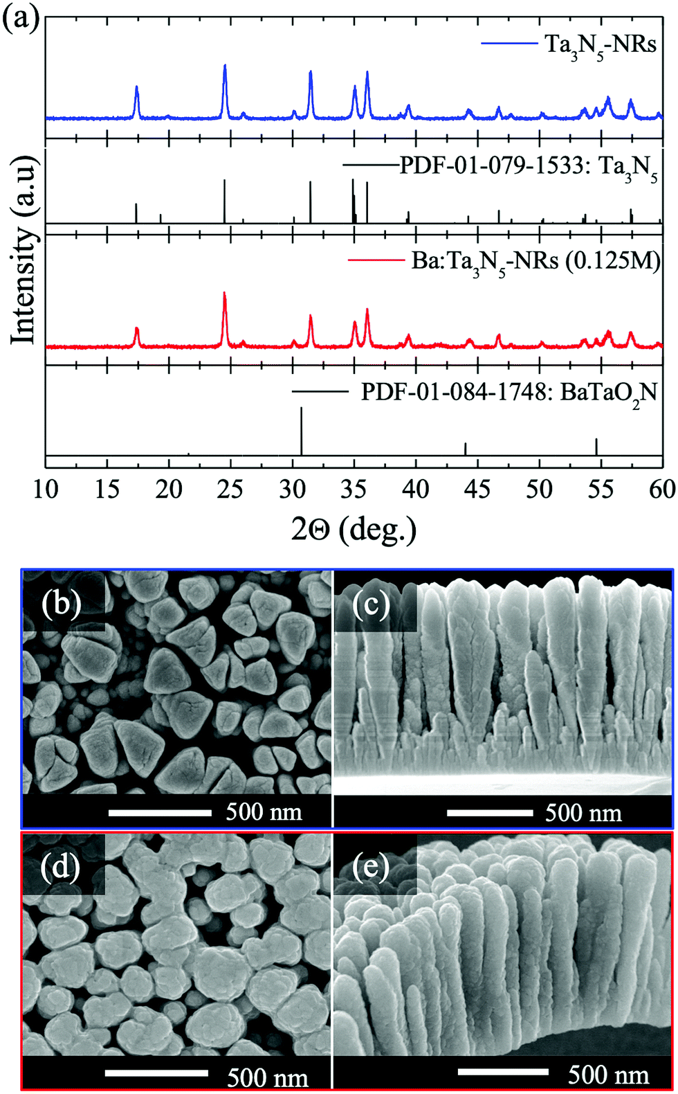 | ||
| Fig. 1 Structures and morphological properties of the Ta3N5-NRs and Ba:Ta3N5-NRs specimens. (a) X-ray diffraction patterns. Top and cross-sectional SEM images of the (b and c) Ta3N5-NRs and (d and e) Ba:Ta3N5-NRs. | ||
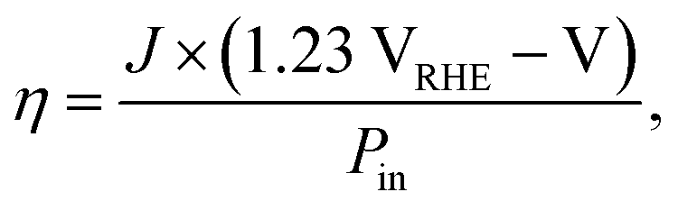
Prior to photoelectrochemical (PEC) measurements using previously reported protocols,20,21 the Ta/Ba:Ta3N5-NRs specimens were uniformly coated with FeNiOx as a co-catalyst (see the EDS elemental map in Fig. S6, ESI†) to prevent photo-corrosion of the NRs surfaces as well as to facilitate the oxygen evolution reaction. The procedure for the co-catalyst loading is also provided in the ESI,† along with details regarding characterization of the materials. Fig. 2 shows the PEC performance of the Ta/Ba:Ta3N5-NRs/FeNiOx photoanode and compares it with that recently reported by our group for a Ta/Ta3N5-NRs/FeNiOx photoanode.20 Fig. S7, ESI† demonstrates that the PEC performance of the Ba:Ta3N5-NRs photoanode was affected by the Ba precursor concentration and that the best performance was obtained at a concentration of 0.125 M. Since the dimensions of the NRs in the Ba:Ta3N5-NRs were similar to those of the Ta3N5-NRs, these materials could be used to examine the effects of Ba doping on the Ta3N5 physical properties and the resultant impact on PEC performance. The current–potential (J–V) curves acquired under chopped AM1.5G simulated solar radiation shown in Fig. 2a indicate that Ba doping of the Ta3N5-NRs photoanode resulted in a 72% increase in the photocurrent density at 1.23 VRHE (Ja), from 3.2 to 5.5 mA cm-2. However, no change in the onset potential (VON) of 0.6 VRHE and a slight decrease in the fill factor (FF), from 30% to 23%, are also evident. The FF values were determined from the relationship FF = Jm(1.23 VRHE − Vm)/Ja(1.23 VRHE − VON),21 where the numerator is the maximum power obtained from the current density, Jm, at an applied potential of Vm (vs. a reference hydrogen electrode (RHE)) for water oxidation. The half-cell (HC) STH efficiency, η, of each photoanode was calculated as:
 | ||
| Fig. 2 Photoelectrochemical properties of the Ta3N5-NRs/FeNiOx and Ba:Ta3N5-NRs/FeNiOx photoanodes. (a) Current–potential (J–V) curves acquired at a potential scan rate of 10 mV s−1 under chopped AM1.5G simulated solar light. (b) Half-cell solar-to-hydrogen (HC-STH) energy conversion efficiency data. (c) IPCE spectra obtained at 1.23 VRHE. (d) Integrated photocurrent densities under AM1.5G simulated solar light (ASTM G173-03) in an electrolyte consisting of 0.5 M KH2PO4 adjusted to a pH of 13 with KOH. The data show that Ba doping improved the performance of the Ta3N5 photoanode by enhancing the IPCE. | ||
Incident photon-to-current efficiency (IPCE) spectra were generated to allow a qualitative assessment of the origin of the photocurrent gain at 1.23 VRHE, which was the primary cause of the increased ηmax value of the Ba:Ta3N5-NRs photoanode. Fig. 2c demonstrates that the Ba:Ta3N5-NRs photoanode exhibited relatively high IPCE values of 40–48% up to 550 nm compared with the Ta3N5-NRs photoanode. This result suggests that Ba doping improved both the separation and transport efficiency of bulk photogenerated charge carriers inside the NRs at an applied potential of 1.23 VRHE. These IPCE spectra also establish that the light absorption edges of both samples were close to 620 nm, meaning that the optical band gap of the Ta3N5 was not affected by Ba doping. Integrated current density, JI, was estimated by numerical integration of the product of the IPCE and the AM1.5G solar spectrum intensity values, S(λ), at various excitation wavelengths, as per the relationship

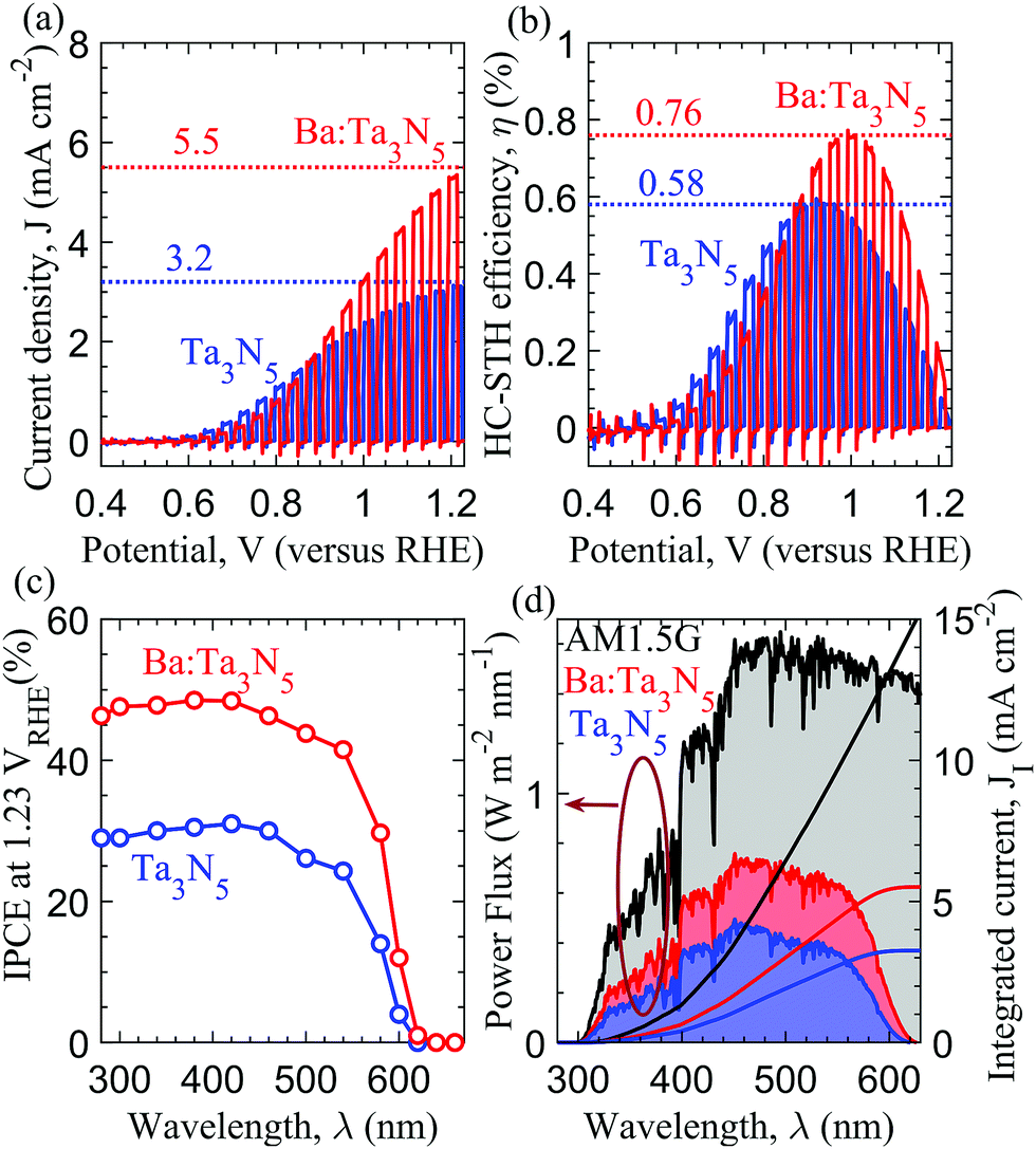
Detailed numerical simulations of optoelectrical properties were performed to investigate the experimentally determined current potential characteristics of the Ba:Ta3N5-NRs and Ta3N5-NRs photoanodes. The goal of this analysis was to examine various performance loss mechanisms as well as to ascertain the most important physical parameters of the photoanodes. An additional aim was to elucidate the role played by Ba doping in providing the observed efficiency enhancement. The simulation methodology is provided in the ESI,† while a schematic diagram and the material parameters that were employed for the Ba:Ta3N5-NRs and Ta3N5-NRs photoanode models are presented in Fig. S10 and Table S2 of ESI.†Fig. 3 displays the results obtained from optical and electrical simulations of the two photoanodes. The results in Fig. 3a indicate that the simulated light absorption (Abs.) was limited by the degree of reflection loss (RL) at shorter wavelengths (<500 nm), while the transmission loss (TL) was greater at longer wavelengths (>550 nm). The significant differences between the simulated light absorption values and the experimental IPCE data at 1.23 VRHE indicate a high level of charge carrier recombination in the Ba:Ta3N5-NRs and Ta3N5-NRs photoanodes. To verify this, the bimolecular radiative recombination (RR) rate coefficient, kr, was fixed and the trap assisted Shockley–Read–Hall (SRH) recombination was tuned by varying the SRH carrier lifetime, τ. The effect of this factor on the simulated current density Ja at 1.23 VRHE is displayed in Fig. 3b, which indicates that the Ja initially increased but eventually plateaued with increases in τ at a given ND. In addition to optical losses (i.e., RL and TL), the Ja was limited by SRH recombination and RR (∝ND) (at low and high τ values, respectively). A substantial improvement in Ja was associated with an order of magnitude reduction in ND in the case of the Ta3N5-NR photoanode within the low τ regime (from 10 ps to 1 ns). A comparison of the simulated Ja with the experimental data found carrier lifetimes, τ, of 0.25 ns and 3 ps for the Ba:Ta3N5-NRs and Ta3N5-NRs photoanodes, respectively.
 | ||
| Fig. 3 Optical and electrical simulations of Ta3N5-NRs and Ba:Ta3N5-NRs photoanodes. (a) Mapping of absorption (Abs.), transmission loss (TL) and reflection loss (RL) values along with the measured incident to photon current efficiencies at 1.23 VRHE (IPCEs). (b) The effects of trap-assisted Shockley–Read–Hall (SRH) recombination on the current density Ja at 1.23 VRHE. (c) Model calibration (with simulation results in black) based on experimental chopped current potential data. (d) A simulated energy band diagram. (e) Hole density, p, electron density, n, and extracted flux values for different carrier generation rates, G, and recombination rates, R, across the specimen diameter 200 nm from the top of the NR. (f) Normalized contributions to current density of optical, radiative and SRH recombination, series resistance, Rs, loss and extracted holes at the NR surfaces during the OER. Respective contributions are normalized to theoretical current limit of 14.55 mA cm−2 for light absorption edge of 620 nm. Ba doping improved the SRH carrier lifetime, τ, by passivating the defect states and so reducing bulk recombination losses and enhancing the photocurrent density at 1.23 VRHE. | ||
Fig. 3c shows the calibration of the model to the measured current–potential characteristics of the photoanodes and confirms good agreement between the theoretical results and experimental data. The values of the various parameters, including τ, effective carrier lifetime (τeff = 1/(krND + 1/τ)), diffusion length ( , where D is the diffusion coefficient), hole extraction rate, Sh, and series resistance, Rs, for the photoanodes are summarized in Table S3, ESI.† These results demonstrate that Ba doping increased both τeff and Rs, which in turn increased the current density at 1.23 VRHE and reduced the FF value, respectively. A decrease in Sh evidently compensated for the effect of the negative shift of VFB on the PEC performance, such that there was almost no change in VON after Ba doping. Fig. 3d shows that the depletion width near the NR surface was decreased by Ba doping of the Ta3N5-NRs, owing to a nearly 10-fold increase in ND. In addition, the extent of band bending across the depletion width was reduced as the surface potential of the NRs was lowered upon changing the applied potential from 1.23 to 0.61 VRHE.
Fig. 3e presents various insights into the charge carrier dynamics of the Ba:Ta3N5-NRs and Ta3N5-NRs photoanodes. At 1.23 VRHE, the high electron density, n (approximately equal to ND), inside the bulk NRs was not affected, whereas the minority hole density, p, increased with increases in the rate at which photogenerated charge carriers were formed, G. This effect ultimately resulted in splitting of the quasi-Fermi energy levels for electrons, Efn, and holes, Efp, as seen in Fig. 3d, such that Efn − Efp ∝ log(Gτeff). The generation of charge carriers caused a negative shift in the holes quasi-Fermi energy level, Efp. The longer lifetime of carriers in the Ba:Ta3N5-NRs caused a greater negative shift in Efp after Ba doping and so the driving force for hole extraction was increased. Because the current density will correlate with the flux of extracted holes from the NRs surfaces, the extracted flux values calculated from the differences in the rates of charge carrier generation, G, and recombination, R, are plotted in Fig. 3e. These data indicate that the bulk charge carriers were extracted more efficiently in the Ba:Ta3N5-NRs than in the Ta3N5-NRs photoanode. However, the reduced Sh led to the accumulation of minority holes near the NR surfaces, which in turn increased the SRH recombination at locations where n = p in the case of the Ba:Ta3N5-NRs photoanode. The enhanced current density generated by the Ba-doped sample is attributed to the positive effect of the increased charge carrier diffusion length, LD (from 3 to 28 nm) rather than the relatively less severe negative effect of surface recombination associated with charge extraction. In contrast, the current density produced by the undoped sample was limited by the extent of bulk charge carrier SRH recombination rather than surface recombination. Fig. 3f summarizes the effects of the various proposed loss processes, including optical, RR, SRH recombination and series resistance, Rs, losses as well as the contribution of extracted charge carriers to the current at 1.23 VRHE for the photoanodes. Ba doping significantly reduced the proportion of the SRH recombination loss, from 46% to 23%, while the bi-molecular radiative recombination (RR) loss was increased from 4% to 8%. Based on the fixed optical loss of 22%, the improved current density observed after Ba doping is attributed primarily to the lower SRH recombination loss. In addition, the increased resistive loss generated lower FF values for the Ba:Ta3N5-NRs photoanode and the decreased hole extraction rate suppressed the effect of the observed negative shift in VFB on VON.
The validity of these suggested explanations for the effects of Ba doping on performance are confirmed by the data in Fig. 4. This figure presents current–potential data previously reported for Ta3N5-NRs and Ba:Ta3N5-NRs photoanodes.22 These data are based on new physical dimensions for the NRs comprising a uniform diameter of 60 nm along with a length of 600 nm, obtained from SEM images of the reported samples. The material parameters employed during the electrical simulations are provided in Table S2, ESI.†Fig. 4a confirms that the simulated light absorption was limited by RL in the short wavelength regime (<400 nm), whereas increased TL and RL effects further reduced the light absorption at longer wavelengths (>400 nm). At 1.23 VRHE, the charge transport was relatively efficient compared with our photoanodes, based on the reduced recombination of charge carriers inside the Ba:Ta3N5-NRs, as is evident from the differences in the simulated light absorption and experimental IPCE values. Similar to Fig. 3b, the current density Ja at 1.23 VRHE increased and eventually plateaued with increases in carrier lifetime, τ. The plateau current in the high τ regime was solely determined by the significant optical losses, whereas additional trap assisted charge carrier recombination reduced the current in the low τ regime. By mapping the experimental data, we obtained τ = 0.3 ns and τ = 50 ps for the previously reported Ba:Ta3N5-NRs and Ta3N5-NRs photoanodes. Using these τ, the model was further calibrated by fine tuning of the hole extraction rate, Sh, and series resistance, Rs, to ensure a close agreement with the experimental VON and FF, respectively. Fig. 4c indicates that the simulated and experimental current–potential characteristics were in reasonable agreement. The material parameters obtained from the model recalibration are summarized in Table S3, ESI.† The maximum theoretical limit of the current density was determined to be 13.16 mA cm-2 based on the band absorption edge of 600 nm in Fig. 4d, and calculations showed that a significant current of nearly 5.4 mA cm−2 was lost through the 41% contribution of optical losses (from both RL and TL). In addition to optical losses, trap assisted SRH recombination losses of approximately 5% and 16% inside the NRs decreased the Ja to 6.78 and 5.22 mA cm−2 for the Ba:Ta3N5:NRs and Ta3N5-NRs photoanodes, respectively. From Fig. 3(b, f) and 4(b, d), it is evident that Ba doping of the Ta3N5-NRs increased the carrier lifetime and hence the diffusion length (see Table S3, ESI†). Thus, limiting the extent of recombination ensured the efficient extraction of charge carriers for enhanced PEC performance.
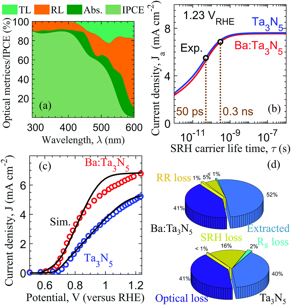 | ||
| Fig. 4 Model recalibration based on data reported for Ta3N5-NRs and Ba:Ta3N5-NRs photoanodes.22 (a) Mapping of simulated optical metrics (transmission loss: TL, reflection loss: RL, light absorption: Abs.) and IPCE data at 1.23 VRHE for a Ba:Ta3N5-NRs photoanode as functions of wavelength. (b) Effects of trap assisted recombination (experimental data: Exp.). (c) Simulated (solid line) and reported (circles) current potential curves. (d) Quantification of various loss mechanisms, including optical (sum of RL and TL), radiative recombination (RR), SRH recombination, and series resistive, along with the extracted output at 1.23 VRHE from Ta3N5-NRs and Ba:Ta3N5-NRs photoanodes. Enhanced photocurrent density is attributed to reduced trap assisted recombination losses following Ba doping of the Ta3N5-NRs. | ||
Discussion
The PEC performance of each Ta3N5-NRs photoanode was determined by the amount of light absorbed to generate charge carriers inside the NRs and the ability of charge carriers to migrate to the NRs surfaces so as to be extracted by the electrolyte and facilitate the OER at various applied potentials. Light absorption by the NRs is limited by the optical losses (TL and RL) which therefore determine the maximum achievable photocurrent for a given morphology. As an example, increasing the NRs length from 600 nm (Fig. 4) to 1000 nm (Fig. 3) enhanced the light absorption and improved the maximum photocurrent from 7.8 to 10.5 mA cm−2, with no recombination losses or 100% internal quantum efficiency. Apart from optical losses, the photocurrent could be further lowered by the bimolecular and/or trap assisted SRH recombination of charge carriers. For efficient charge extraction, the NRs radius should be comparable to the diffusion length of the charge carriers to minimize the recombination loss. Despite the asymmetric transport of holes to the NRs surface and of electrons toward the substrate, Fig. 3f indicates a significant recombination loss of nearly 32% (based on RR and SRH) at NRs radius values of 85 nm in the case of the Ba-doped samples. This radius exceeds the estimated diffusion length of 27.88 nm. In contrast, in Fig. 4d, the recombination loss is decreased to 6% when NRs radius (30 nm) is comparable to the diffusion length (29 nm). These results demonstrate that the structural optimization of the NRs through length and diameter tailoring is essential to suppressing optical and recombination losses with the aim of improving the performance of Ta3N5-NRs photoanodes. Fig. 3 and 4 also confirm that Ba doping increased the effective charge carrier lifetime, τeff, and diffusion length, LD, and hence reduced the recombination losses and improved the photocurrent density at 1.23 VRHE of the Ba:Ta3N5-NRs photoanode for a given NR radius. Previously, we reported that these Ta3N5-NRs contain numerous polycrystalline domains (i.e., grains) of Ta3N5 separated by defective grain boundaries.21 These boundaries can act as trapping or recombination centres for mobile charge carriers. We believe that Ba doping passivates the defect states associated with these grain boundaries, so that the effective carrier lifetime and thereby the diffusion length are increased. Similar passivation strategies based on the doping of grain boundaries have often been employed to maximize the performance of photovoltaic technologies based on perovskites,33–35 Cu(In, Ga)Se236–40 (CIGS) and other materials. In addition to the experimental evidence, the numerical calculations demonstrated that the passivation of defect states at grain boundaries would be expected to increase carrier lifetimes as in perovskite solar cells and CIGS-based photocathodes leading to enhanced device performance.41–44 Therefore, it is imperative to simultaneously engineer the NRs dimensions and material properties related to defect states to ensure efficient light absorption and charge extraction.The maximum HC-STH efficiency, ηmax, of a photoanode will be proportional to the product of the current density Ja with FF and relative difference of VON from 1.23 VRHE, and the present work shows that the FF could be reduced as a consequence of resistive loss in the fabricated samples. This resistive effect originated from the cumulative resistances of the substrate and the Ta3N5-NRs as well as charge transfer from the NRs surface to the electrolyte, which can be decoupled using bias dependent impedance spectroscopy data. Despite the increased electrical conductivity resulting from Ba doping of the NRs, in Fig. 3, the increase in the resistive losses reduced the FF, suggesting that the Ta3N5-NRs were not the limiting resistance element in this photoanode. Because the Ta substrate was highly conductive, the resistive loss is believed to have been associated with the charge transfer resistance. In addition to bulk recombination, the onset potential is determined by the recombination of charge carriers near the NRs surface, and this surface recombination originates from hole accumulation due to a low hole transfer rate, Sh. Therefore, a careful optimization of the NRs surface is a critical aspect of improving FF and VON, which in turn would improve ηmax.
Based on the above discussion, Fig. 5 displays a predictive roadmap related to the goal of achieving an HC-STH efficiency, ηmax, of more than 10% to allow commercialization of nanostructured Ta3N5-NRs photoanodes. This map uses the calibrated model constructed for the undoped Ta3N5-NRs photoanode shown in Fig. 4c as the starting point. Employing a fixed NR diameter of 60 nm, the NR length, L, was varied linearly from 600 to 2000 nm, which was associated with a logarithmic increase in the carrier lifetime, τ, from 50 ps to 50 ns, a linear decrease in the series resistance, Rs, from 50 to 0 Ω cm2, and a logarithmic increase in the hole extraction rate, Sh, from 3.5 × 10⁻³ to 350 cm s−1. HC-STH efficiency values, ηmax, were calculated from the simulated current–potential characteristics and are plotted against the variations in L, τ, Rs and Sh in Fig. 5. For reference purposes, data for the Ta3N5 photoanodes having the highest reported ηmax values (since 2013) are also included.15,21,22 This figure confirms that the highest reported HC-STH efficiency of 2.72% is still far from the required value of 10%, which indicates that significant optimizations of the anode structure and composition are required. As an example, Fig. 5a demonstrates that a Ta3N5-NRs photoanode has the potential to exhibit an HC-STH efficiency of more than 10% based on the cumulative effects of increasing the NR length and the carrier lifetime, τ, while decreasing the resistance, Rs, and improving the hole extraction rate, Sh. In Fig. 5b, we show that the current density at 1.23 VRHE, Ja, is improved with increases in L and the carrier lifetime, τ, whereas the fill factor, FF, is optimized by eliminating the series resistance, Rs, and the onset potential, VON, is lowered by increases in the carrier lifetime, τ, and hole extraction rate, Sh. These effects of structural and material parameters on performance can therefore work together to give an HC-STH efficiency in excess of 10%.
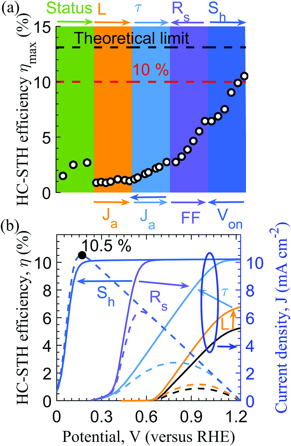 | ||
| Fig. 5 Predictive design strategies to meet the market requirement of a 10% HC-STH efficiency for Ta3N5-NRs photoanodes. The first window in (a) indicates the highest reported HC-STH efficiencies since 2013.15,21,22 The calibrated model for an Ta3N5-NRs photoanode shown in Fig. 4 was employed as the base model to explore the effects of the NR length, L, carrier lifetime, τ, series resistance, Rs, and hole extraction rate, Sh in respective windows. The arrows at the top and base of the diagram respectively indicate increases in the parameters and the resulting effects on performance metrics. (b) Effect of optimized L, τ, Rs, and Sh on performance characteristics. Direction of arrows represent the increase in respective parameters from low to high values. | ||
Based on above design principles, we refabricated the Ta3N5-NRs photoanodes with a special focus on improving the quality of the Ta3N5 to increase the carrier lifetime, τ, and so improve the performance based on the information in Fig. 5b. The newly fabricated Ta3N5-NRs were prepared under different processing conditions than were used to synthesize the Ta3N5-NRs sample shown in Fig. 1. Table S4, ESI† compares the various GLAD parameters and nitridation conditions for the respective samples. Specifically, a mixed Ar/N2 plasma was employed to deposit TaNx-NRs on a Ta substrate, which was then subjected to nitridation at 950, 980 or 1000 °C to obtain Ta3N5-NRs. In contrast, the Ta-NRs shown in Fig. 1 were deposited using an Ar plasma to obtain Ta3N5-NRs after nitridation at 980 °C. The SEM images in Fig. 6(a) and (b) show that the morphology of the Ta3N5-NRs obtained from the mixed plasma was slightly different from that of the material made with the pure Ar plasma. However, the Ta3N5-NRs were still vertically aligned and separated with similar lengths and maximum diameters. The XRD, EDS and XPS results in Fig. (S11–S13), ESI† demonstrate that the crystalline phase of this new Ta3N5, its uniform distribution over the substrate and its elemental composition were all similar to those described in previous reports.21,22 Despite the different morphologies of the specimens produced using the two types of plasma, the new Ta3N5-NRs were able to promote water oxidation based on similar asymmetric charge transport in the bulk of the material, meaning that photogenerated electrons migrated to the Ta substrate while holes moved to the NRs surface.
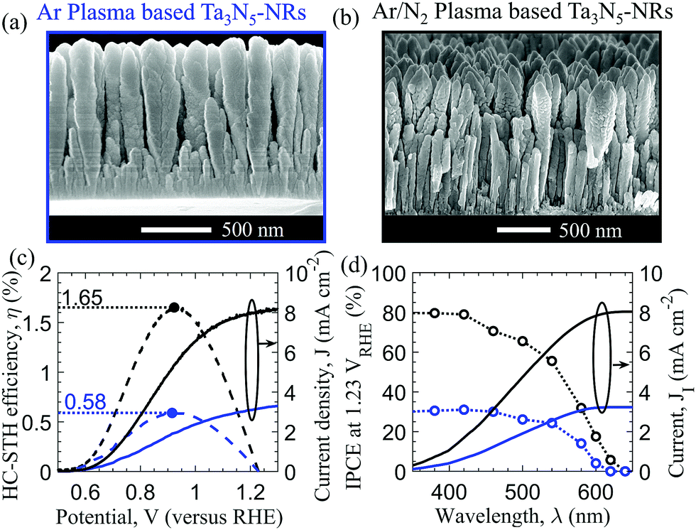 | ||
| Fig. 6 Performance enhancement of a Ta3N5-NRs/FeNiOx photoanode. SEM image of Ta3N5-NRs prepared using (a) an Ar plasma and (b) a mixed Ar/N2 plasma. (c) HC-STH efficiency η and current potential (J–V) characteristics under continuous AM1.5G solar light along with the (d) the IPCE spectrum and integrated photocurrent density values (at an electrolyte pH of 13). Blue and black plots correspond to the Ar plasma and mixed plasma based Ta3N5-NRs/FeNiOx photoanodes, respectively. | ||
After loading with the FeNiOx co-catalyst (Fig. S12, ESI†), the Ta3N5-NRs/FeNiOx photoanode was evaluated by PEC measurements. The data in Fig. S14, ESI† confirm that the nitridation temperature affected the performance of the photoanode, with a temperature of 980 °C being optimal. Fig. 6c indicates that the optimized mixed plasma photoanode generated a higher photocurrent density of 8 mA cm−2 at 1.23 VRHE compared with the materials made using an Ar plasma. Consequently, the maximum HC-STH efficiency of the photoanode during water oxidation was improved from 0.58% to 1.65%. This enhanced performance is ascribed to increased charge separation and transport efficiency (as is evident from the IPCE spectrum in Fig. 6d), both of which are believed to have resulted from increase in the carrier lifetime, τ. Compared to Ar plasma based Ta3N5-NRs photoanode, the improvement in τ is suspected to be originated from the suppressed oxygen impurities (see Fig. S4b and S13b, ESI†) in mixed plasma based photoanode. From the theoretical predictions in Fig. 5b, it is apparent that increases in the carrier lifetime, τ, can increase the photocurrent density, Ja, at 1.23 VRHE and also decrease the onset potential, Von. The fabricated mixed plasma based photoanodes showed appreciable improvement in photocurrent density at 1.23 VRHE, although the onset potential is merely got affected. We believe that this discrepancy between the theoretical prediction and experimental outcome regarding the onset potential might originate from the limited hole extraction rate from the NR surfaces. As an example, the expected decrease in onset potential with increases in the carrier lifetime could have been inhibited by an increase in the recombination of charge carriers at the NR surfaces resulting from a decreased hole extraction rate. As noted earlier, both the NRs dimensions and materials should be tailored simultaneously to realize highly efficient Ta3N5-NRs photoanodes. In future, we will focus our research efforts on controlling the dimensions of NRs in the mixed plasma material such that the radius of these NRs is similar to the charge diffusion length, as a means of achieving the predicted maximum efficiency. This future work will also involve the use of an optimal co-catalyst to possibly decrease the onset potential and improve the stability of these Ta3N5-NRs photoanodes.
Conclusions
This work carried out optoelectrical simulations to investigate the different loss mechanisms responsible for the current–potential characteristics of Ba-doped and undoped Ta3N5-NRs photoanodes. A vertically aligned, well separated Ba-doped Ta3N5-NRs photoanode was fabricated. The results showed that Ba doping improved the photocurrent density at 1.23 VRHE and hence the HC-STH efficiency, in agreement with previous reports. A theoretical model was calibrated using multiple experimental data sets to quantify the different loss mechanisms, including optical, charge carrier recombination and resistive losses at 1.23 VRHE for photoanodes fabricated in the present work and made previously. The resulting model was employed to predict performance limiting parameters including the charge carrier lifetime, diffusion length, hole extraction rate and series resistance. The results indicated that Ba doping would be expected to passivate defect states to increase both the carrier lifetime and diffusion length. Greater diffusion lengths in turn were predicted to reduce the rate of charge carrier recombination to provide more efficient charge transport and improved HC-STH efficiency. This research also demonstrated that both optical and recombination losses can be suppressed by increasing and decreasing the NR lengths and diameters, respectively. Probing the fundamental loss mechanisms and identifying the performance limiting parameters in this manner provided theoretical guidelines showing that optimizations of both structure and materials will be required to realize highly efficient Ta3N5-NRs photoanodes. Consequently, we improved the component materials and raised the HC-STH efficiency from 0.58% to 1.65%. This outcome provides an experimental demonstration of the proposed theoretical performance gains based on improved carrier lifetimes in Ta3N5-NRs photoanodes.Conflicts of interest
There are no conflicts to declare.Acknowledgements
This work was supported by the Research Project for Future Development: Artificial Photosynthetic Chemical Process (ARPChem), METI/NEDO, Japan (2012–2022).References
- S. Dahl and I. Chorkendorff, Nat. Mater., 2012, 11, 100–101 Search PubMed.
- R. E. Blankenship, D. M. Tiede, J. Barber, G. W. Brudvig, G. Fleming, M. Ghirardi, M. R. Gunner, W. Junge, D. M. Kramer, A. Melis, T. A. Moore, C. C. Moser, D. G. Nocera, A. J. Nozik, D. R. Ort, W. W. Parson, R. C. Prince and R. T. Sayre, Science, 2011, 332, 805–809 Search PubMed.
- M. G. Walter, E. L. Warren, J. R. McKone, S. W. Boettcher, Q. Mi, E. A. Santori and N. S. Lewis, Chem. Rev., 2010, 110, 6446–6473 Search PubMed.
- J. R. McKone, N. S. Lewis and H. B. Gray, Chem. Mater., 2014, 26, 407–414 Search PubMed.
- A. J. Bard and M. A. Fox, Acc. Chem. Res., 1995, 28, 141–145 Search PubMed.
- Y. Tachibana, L. Vayssieres and J. R. Durrant, Nat. Photonics, 2012, 6, 511–518 Search PubMed.
- S. Chen, T. Takata and K. Domen, Nat. Rev. Mater., 2017, 2, 17050 Search PubMed.
- Q. Wang and K. Domen, Chem. Rev., 2020, 120, 919–985 Search PubMed.
- T. Takata, J. Jiang, Y. Sakata, M. Nakabayashi, N. Shibata, V. Nandal, K. Seki, T. Hisatomi and K. Domen, Nature, 2020, 581, 411–414 Search PubMed.
- K. Takanabe, ACS Catal., 2017, 7, 8006–8022 Search PubMed.
- G. Liu, J. Shi, F. Zhang, Z. Chen, J. Han, C. Ding, S. Chen, Z. Wang, H. Han and C. Li, Angew. Chem., Int. Ed., 2014, 53, 7295–7299 Search PubMed.
- H. X. Dang, N. T. Hahn, H. S. Park, A. J. Bard and C. B. Mullins, J. Phys. Chem. C, 2012, 116, 19225–19232 Search PubMed.
- D. Yokoyama, H. Hashiguchi, K. Maeda, T. Minegishi, T. Takata, R. Abe, J. Kubota and K. Domen, Thin Solid Films, 2011, 519, 2087–2092 Search PubMed.
- M. Higashi, K. Domen and R. Abe, Energy Environ. Sci., 2011, 4, 4138–4147 Search PubMed.
- G. Liu, S. Ye, P. Yan, F. Xiong, P. Fu, Z. Wang, Z. Chen, J. Shi and C. Li, Energy Environ. Sci., 2016, 9, 1327–1334 Search PubMed.
- M. Zhong, T. Hisatomi, Y. Sasaki, S. Suzuki, K. Teshima, M. Nakabayashi, N. Shibata, H. Nishiyama, M. Katayama, T. Yamada and K. Domen, Angew. Chem., Int. Ed., 2017, 56, 4739–4743 Search PubMed.
- P. Zhang, T. Wang, J. Zhang, X. Chang and J. Gong, Nanoscale, 2015, 7, 13153–13158 Search PubMed.
- I. Narkeviciute, P. Chakthranont, A. J. M. MacKus, C. Hahn, B. A. Pinaud, S. F. Bent and T. F. Jaramillo, Nano Lett., 2016, 16, 7565–7572 Search PubMed.
- Y. Li, T. Takata, D. Cha, K. Takanabe, T. Minegishi, J. Kubota and K. Domen, Adv. Mater., 2013, 25, 125–131 Search PubMed.
- Y. Pihosh, V. Nandal, T. Minegishi, M. Katayama, T. Yamada, K. Seki, M. Sugiyama and K. Domen, ACS Energy Lett., 2020, 5, 2492–2497 Search PubMed.
- Y. Pihosh, T. Minegishi, V. Nandal, T. Higashi, M. Katayama, T. Yamada, Y. Sasaki, K. Seki, Y. Suzuki, M. Nakabayashi, M. Sugiyama and K. Domen, Energy Environ. Sci., 2020, 13, 1519–1530 Search PubMed.
- Y. Li, L. Zhang, A. Torres-Pardo, J. M. González-Calbet, Y. Ma, P. Oleynikov, O. Terasaki, S. Asahina, M. Shima, D. Cha, L. Zhao, K. Takanabe, J. Kubota and K. Domen, Nat. Commun., 2013, 4, 2566 Search PubMed.
- J. Seo, T. Takata, M. Nakabayashi, T. Hisatomi, N. Shibata, T. Minegishi and K. Domen, J. Am. Chem. Soc., 2015, 137, 12780–12783 Search PubMed.
- Y. Kado, C. Y. Lee, K. Lee, J. Müller, M. Moll, E. Spiecker and P. Schmuki, Chem. Commun., 2012, 48, 8685–8687 Search PubMed.
- Y. W. Kim, S. Cha, I. Kwak, I. S. Kwon, K. Park, C. S. Jung, E. H. Cha and J. Park, ACS Appl. Mater. Interfaces, 2017, 9, 36715–36722 Search PubMed.
- S. S. K. Ma, T. Hisatomi, K. Maeda, Y. Moriya and K. Domen, J. Am. Chem. Soc., 2012, 134, 19993–19996 Search PubMed.
- H. Hajibabaei, D. J. Little, A. Pandey, D. Wang, Z. Mi and T. W. Hamann, ACS Appl. Mater. Interfaces, 2019, 11, 15457–15466 Search PubMed.
- W. W. Gärtner, Phys. Rev., 1959, 116, 84–87 Search PubMed.
- J. Reichman, Appl. Phys. Lett., 1980, 36, 574–577 Search PubMed.
- Y. Pihosh, I. Turkevych, K. Mawatari, N. Fukuda, R. Ohta, M. Tosa, K. Shimamura, E. G. Villora and T. Kitamori, Nanotechnology, 2014, 25, 315402 Search PubMed.
- S. Kosar, Y. Pihosh, I. Turkevych, K. Mawatari, J. Uemura, Y. Kazoe, K. Makita, T. Sugaya, T. Matsui, D. Fujita, M. Tosa, Y. M. Struk, M. Kondo and T. Kitamori, Jpn. J. Appl. Phys., 2016, 55, 04ES01 Search PubMed.
- Y. Pihosh, J. Uemura, I. Turkevych, K. Mawatari, Y. Kazoe, A. Smirnova and T. Kitamori, Angew. Chem., Int. Ed., 2017, 56, 8130–8133 Search PubMed.
- D. S. Lee, J. S. Yun, J. Kim, A. M. Soufiani, S. Chen, Y. Cho, X. Deng, J. Seidel, S. Lim, S. Huang and A. W. Y. Ho-Baillie, ACS Energy Lett., 2018, 3, 647–654 Search PubMed.
- Q. Guo, F. Yuan, B. Zhang, S. Zhou, J. Zhang, Y. Bai, L. Fan, T. Hayat, A. Alsaedi and Z. Tan, Nanoscale, 2019, 11, 115–124 Search PubMed.
- G. Li, X. Zou, J. Cheng, X. Bai, D. Chen, Y. Yao, C. Chang, X. Yu, Z. Zhou, J. Wang and B. Liu, Mater. Lett., 2020, 273, 127979 Search PubMed.
- N. Nicoara, T. Lepetit, L. Arzel, S. Harel, N. Barreau and S. Sadewasser, Sci. Rep., 2017, 7, 41361 Search PubMed.
- P. Reinhard, B. Bissig, F. Pianezzi, E. Avancini, H. Hagendorfer, D. Keller, P. Fuchs, M. Döbeli, C. Vigo, P. Crivelli, S. Nishiwaki, S. Buecheler and A. N. Tiwari, Chem. Mater., 2015, 27, 5755–5764 Search PubMed.
- F. Pianezzi, P. Reinhard, A. Chirila, B. Bissig, S. Nishiwaki, S. Buecheler and A. N. Tiwari, Phys. Chem. Chem. Phys., 2014, 16, 8843–8851 Search PubMed.
- D. Rudmann, A. F. da Cunha, M. Kaelin, F. Kurdesau, H. Zogg, A. N. Tiwari and G. Bilger, Appl. Phys. Lett., 2004, 84, 1129–1131 Search PubMed.
- L. Anke, W. Roland and P. Michael, Phys. Status Solidi RRL, 2013, 7, 631–634 Search PubMed.
- V. Nandal and P. R. Nair, J. Appl. Phys., 2019, 125, 173110 Search PubMed.
- V. Nandal and P. R. Nair, ACS Nano, 2017, 11, 11505–11512 Search PubMed.
- V. Nandal and P. R. Nair, J. Phys. Chem. C, 2018, 122(49), 27935–27940 Search PubMed.
- V. Nandal, Y. Suzuki, H. Kobayashi, K. Domen and K. Seki, J. Mater. Chem. A, 2020, 8, 9194–9201 Search PubMed.
Footnotes |
| † Electronic supplementary information (ESI) available: Estimation of maximum theoretical STH efficiency of Ta3N5. Details of fabrication processes, conditions; and characterizations. XRD, XPS, and EDS analysis. Procedure of FeNiOx co-catalyst loading. Mott–Schottky analysis. Evolution of H2 and O2 gases measured by gas chromatography. Methodology of optical and electrical simulations along with the details of employed material parameters. Extracted material parameters from optoelectrical model calibration. See DOI: 10.1039/d1ee01004b |
| ‡ Authors with equal contribution. |
| This journal is © The Royal Society of Chemistry 2021 |