
 Open Access Article
 This Open Access Article is licensed under a Creative Commons Attribution-Non Commercial 3.0 Unported Licence
Designing efficient spin Seebeck-based thermoelectric devices via simultaneous optimization of bulk and interface properties†
Min Young
Kim
 a,
Sang J.
Park
a,
Gi-Yeop
Kim
bc,
Si-Young
Choi
bc and
Hyungyu
Jin
*a
a,
Sang J.
Park
a,
Gi-Yeop
Kim
bc,
Si-Young
Choi
bc and
Hyungyu
Jin
*a
aDepartment of Mechanical Engineering, Pohang University of Science and Technology (POSTECH), Pohang 37673, South Korea. E-mail: hgjin@postech.ac.kr
bDepartment of Materials Science and Engineering, Pohang University of Science and Technology (POSTECH), Pohang 37673, South Korea
cMaterials Imaging & Analysis Center, Pohang University of Science and Technology (POSTECH), Pohang 37673, South Korea
First published on 29th April 2021
Abstract
The spin Seebeck effect (SSE) refers to a direct energy conversion of heat to electricity that exploits magnon current in a ferromagnet (FM)/normal metal (NM) heterostructure. Since SSE is a transverse thermoelectric effect, it can be employed to realize transverse thermoelectric devices, which could potentially overcome the inherent limitations of conventional Seebeck effect-based devices. Yet, the widespread use of SSE is currently hindered by its low conversion efficiency. The thermoelectric efficiency of SSE can be improved through an optimization of bulk FM as well as FM/NM interface. A bulk FM can enhance the thermoelectric efficiency by introducing a ‘phonon-glass magnon-crystal’ concept, wherein scattering centers selectively scatter the heat-carrying phonons while not affecting the magnons that contribute to SSE. A high-quality FM/NM interface can boost the spin pumping across the interface as well as the electrical transport in NM. Here, by adopting polycrystalline nickel-ferrite (NFO)/Pt as a platform, we demonstrate the successful optimization of bulk FM together with FM/NM interface via a simple heat treatment scheme. The phase separation of NFO via such heat treatment results in a distinctive hierarchical microstructure of nano-sized NFO embedded in micro-sized NiO precipitates; this structure selectively scatters phonons while barely affecting magnons, leading to reduced thermal conductivity without variation of spin Seebeck coefficient. The simultaneous formation of a clean and smooth NFO/Pt interface provides efficient spin pumping at the interface and high electrical conductivity of Pt. As a result, the energy conversion efficiency of SSE in NFO/Pt system can be significantly improved. The proposed facile approach can be applied to design highly efficient oxide-based SSE devices.
Broader contextThermoelectric (TE) conversion offers a carbon-free power generation from waste heat, which can contribute to mitigating both energy and climate challenges. The current TE power generation relies on the charge Seebeck effect, which requires a complex device geometry. It is possible to make the device structure much simpler if the TE device can be constructed by utilizing a transverse TE effect where a charge current is generated in the direction perpendicular to the applied temperature gradient. The spin Seebeck effect (SSE) is a suitable candidate for realizing such a transverse TE device, although the figure of merit of SSE devices is still 3 to 4 orders of magnitude lower than that of the conventional TE devices. Since the figure of merit of an SSE device depends on multiple factors, optimizing it has been considered quite challenging. Here, using a polycrystalline nickel-ferrite (NFO)/Pt bilayer as a platform, we successfully demonstrate a simultaneous optimization of the magnon and phonon transport in bulk NFO and the NFO/Pt interface quality, two crucial factors that determine the figure of merit, via a simple heat treatment scheme. Our study paves a new route towards designing efficient transverse TE devices based on SSE. |
Introduction
The daunting global climate challenges urge deployment of carbon-neutral technologies in each industrial sector. As for the energy sector, an energy conversion process is vital to produce any useful form of energy, e.g., electricity, but at the same time has been a significant source of carbon emission.1 As one potential way to realize a carbon-free power generation from waste heat, thermoelectricity has long been researched over the past century. Thermoelectric power generation is based on the Seebeck effect, wherein a direct conversion of heat-to-electricity happens through an all solid-state device. Thermoelectric devices do not involve any moving parts, working fluids, or chemical reactions, which allows reliable, noiseless, and carbon-free operation.2,3 All of these advantages place the thermoelectric conversion as one of promising next-generation power generation technologies.A typical structure of conventional thermoelectric devices comprises many pairs of n and p-type semiconducting materials connected thermally in parallel and electrically in series. Since the Seebeck effect is a longitudinal thermoelectric effect wherein a charge current is generated in the direction parallel to an applied temperature gradient, the use of both n and p-type materials is required to return the induced charge current to an isothermal plane. Such a longitudinal geometry is inherently complex and thus less manufacturing-friendly. In addition, the requirement of parallel heat and charge flows makes overall performance largely dependent on intrinsic material properties rather than device design parameters. However, an optimization of thermoelectric material is challenging due to the counter-indicated nature of thermoelectric properties and has been one of bottlenecks for widespread use of thermoelectric devices.4,5 These inherent limitations for longitudinal devices will persist regardless of any future research progress in conventional thermoelectrics.
Recently, a concept of transverse thermoelectric energy conversion has been emerging as an alternative to overcome the limitations of the longitudinal counterpart.6–8 In a transverse thermoelectric device, a charge current is generated in the direction perpendicular to the applied temperature gradient, which allows that the device performance scales with extrinsic dimensions. Specifically, the output voltage (power) can be enhanced by simply increasing the device length (surface area) perpendicular to the temperature gradient. This means that the thermoelectric performance can be improved by manipulating device designs, even in the absence of improvement to material properties. In addition, transverse devices do not require the use of separate n and p-type materials, since the plane in which the output voltage arises is always isothermal. Thus, transverse thermoelectric devices can have significantly less complex structure and manufacturing than those of longitudinal devices. Realizing such a transverse device requires to employ a suitable transverse thermoelectric effect that guarantees a sufficiently large conversion efficiency.
The spin Seebeck effect (SSE) refers to a heat-to-electricity energy conversion process via spin current in magnetic material. In general, the SSE requires a simple ferromagnet (FM)/normal metal (NM) bilayer structure,9–16 wherein the following conversion process occurs: first, the spin current of either magnons (when FM is an insulator) or spin-polarized electrons (when FM is a conductor) are generated in the FM in response to an applied temperature gradient and an external magnetic field. The spin current flows across the FM/NM junction via the exchange coupling, i.e., spin pumping, and are subsequently converted into an electric field through the inverse spin Hall effect (ISHE) in the NM layer.17 Experimentally, the electric field, a length-normalized voltage difference, is measured perpendicular to the temperature gradient and magnetic field, which makes SSE suitable for transverse thermoelectric generation.
Over the past years, fundamental aspects of SSE have been studied using yttrium iron garnet (YIG)/Pt platform.18–24 From an engineering perspective, however, the thermoelectric efficiency of SSE, largely determined by the dimensionless figure of merit ZSSET, is still 3 to 4 orders of magnitude lower than that of the conventional thermoelectric counterpart.16 In addition to ZSSET, the thermoelectric efficiency of SSE devices also depends on the thickness ratio between FM and NM as discussed in ref. 16. Therefore, novel approaches should be developed to optimize the both parameters in order to design highly efficient SSE devices for practical application.
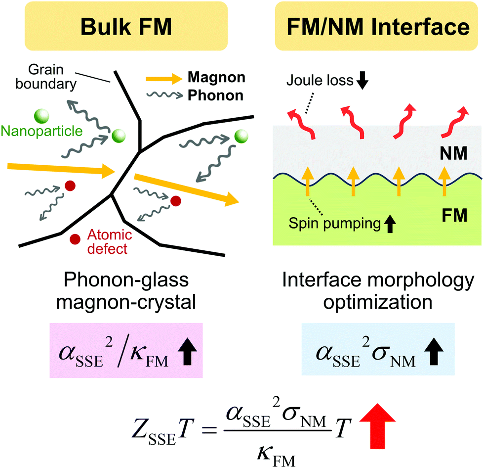
A promising approach to improve ZSSET is to reduce thermal conductivity κFM of the FM layer as well as to increase both spin Seebeck coefficient αSSE of the FM/NM system and electrical conductivity σNM of the NM layer, according to the following relation:16
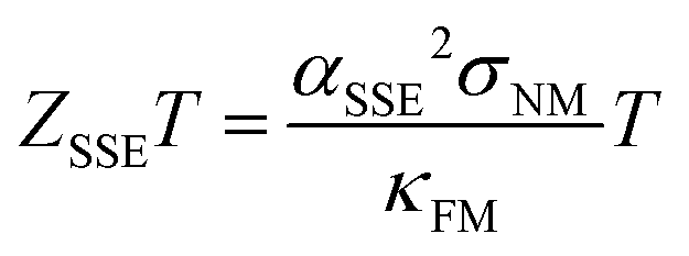 | (1) |
Such strategies can be developed by using a bulk polycrystalline FM/NM system as a platform (Fig. 1). First, the separation of phonon and magnon currents could be achieved by inducing selective scattering mechanisms in the bulk FM; the heat-carrying phonons are effectively scattered while the transport of magnons is not hampered, so αSSE2/κFM can be improved (i.e., lower κFM or raise αSSE). Examples of such scattering sources are nano-particles (or -precipitates), grain boundaries, atomic defects, etc. In that regard, one attempt has been made to introduce nano-sized grains in polycrystalline YIG. Miura et al.23 observed 41% reduction of κFM in the nanostructured YIG compared to that of single-crystalline YIG, whereas they noticed more significant reduction of αSSE by 79%. The SSE signal in bulk YIG at 300 K is dominantly driven by long-wavelength magnons with spin diffusion lengths up to 10 μm,18,24 several orders of magnitude longer than the mean free path of phonons. It is likely that the scattering of those long-wavelength magnons by the nano-sized grains is spin-flipping, significantly reducing the magnon spin diffusion length. The larger suppression of αSSE than κFM suggests that the reduction ratio of the magnon spin diffusion length is larger than that of phonon mean free path in this system.
 | ||
| Fig. 1 Strategies to optimize bulk FM and FM/NM interface properties for improving the figure of merit (ZSSET) of polycrystalline FM/NM systems (FM: ferromagnet, NM: normal metal): introduction of phonon-glass magnon-crystal in the FM and optimization of the FM/NM interface morphology. | ||
Such selective screening between different energy carriers has been a popular topic in conventional thermoelectric research, wherein the main objective is to separately control phonons and electrons, realizing a phonon-glass electron-crystal system. Although many successful cases have been reported in conventional thermoelectrics,25–28 to the best of our knowledge, no success has been demonstrated in SSE-based thermoelectrics yet. In SSE-based thermoelectrics, a ‘phonon-glass magnon-crystal’ concept has to be developed, which requires a careful design of the scattering mechanisms by considering the spectral nature of phonons and magnons. The previous work by Miura et al.23 suggests that nano-sized grains are not an appropriate candidate at least for YIG, as they strongly suppress the propagation of long-wavelength magnons. Since it is difficult to predict whether the scattering nature of a given scattering source will be spin-flipping or not, one possible approach is to introduce scattering centers that simply less scatter the long-wavelength magnons than the heat-carrying phonons. Below we demonstrate that nano-precipitates with the size of tens of nanometers effectively realize the phonon-glass magnon-crystal in polycrystalline NiFe2O4 (NFO).
Next, the optimization of FM/NM interface condition can be achieved by deliberately controlling the FM/NM interface morphology before NM layer deposition. A clean and smooth FM/NM interface generally leads to more efficient spin pumping at the FM/NM interface as well as high-quality NM layer deposition, each resulting in a higher αSSE and σNM (i.e. reduced Joule loss), respectively, and thus an improved αSSE2σNM. For example, Aqeel et al.29 reported that the magnitude of SSE is strongly enhanced by mechanically polishing the surface of YIG single crystal before Pt deposition. Saiga et al.30 investigated the effect of annealing on the SSE signal in polycrystalline YIG/Pt. They showed that the annealing YIG in air at 1073 K before Pt deposition increases the spin Seebeck voltage by 2.8 times that of a non-annealed sample and attributed the increase to the improved interface crystallinity. We also recently conducted a systematic study on the effect of polishing force and annealing temperature on the SSE signal in polycrystalline NFO/Pt, and revealed that mesoscale defects (cracks, pores, and grain grooves) and roughness of interface strongly affect the SSE signal.31
Despite the independent efforts to realize each of the above-mentioned two optimization strategies by different groups, no successful demonstration has been reported thus far to realize both strategies in a single SSE platform. In this study, we use polycrystalline NFO/Pt as our platform to demonstrate a facile realization of both strategies. First, a temperature-dependent phase separation in NFO by a simple heat treatment scheme allows an intriguing hierarchical microstructure to be generated within the bulk NFO matrix. We identify that the hierarchical microstructure consists of many nano-sized NFO precipitates embedded in a micro-sized Fe-doped NiO precipitate. Detailed analyses of microstructure and transport properties reveal that the hierarchical microstructure indeed works as selective scatterers for phonons rather than magnons, leading to the favorable αSSE2/κFM. Next, we also find that the simple heat treatment simultaneously leads to a clean and smooth NFO/Pt interface; the high-quality interface guarantees an enlarged active area fraction and a small roughness of the NFO surface. So, those surface characteristics enable efficient spin pumping at the interface as well as high-quality Pt deposition, resulting in the increased αSSE2σNM.
Experimental
Synthesis of bulk NFO polycrystals
All NFO polycrystals were prepared using a powder metallurgy method. First, NFO nano-powders (99.99%, US Nano Inc.) were uniaxially pressed into three different pellets (12.7 mm in diameter) at 155 MPa (Hydraulic press, Carver Inc.). Then, two-step sintering processes were applied on the three pellets with different temperature profiles (Fig. S1 in ESI†) to control a size and amount of precipitates in the NFO matrix. For comparison, we henceforth label the three samples with their final sintering temperature (1623, 1673, and 1723 K), i.e., NFO1623, NFO1673, and NFO1723. After the sintering processes, each pellet was cut by a diamond wire saw (STX-202A, MTI Korea) into a rectangular slab (2.4 mm × 3.8 mm × ∼0.5 mm) for SSE measurements and a 2 mm-thick disk for thermal diffusivity measurements.Surface treatment of NFO slabs and Pt growth
The fabricated NFO slabs were subjected to the optimized surface treatment, which was reported in our previous work31 and can be summarized as follows. First, all NFO slabs were deliberately polished using an auto polisher (MetPrep 4, Allied High Tech.) with abrasive SiC papers (P400–P4000) and diamond suspensions (3, 1 and 0.25 μm). During the polishing process, polishing force remained constant at 13 N with rotation speed of 150 rpm for 30 min. Then, the polished slabs were post-annealed at 573 K for 3 h to improve their micronized or amorphized surface. After all surface treatments, an e-beam evaporation system (Korea Vacuum Tech.) was used to deposit a 10 nm Pt layer (99.9%, TASCO) on the NFO surface.Thermal conductivity measurements
Thermal conductivity κ of the NFO samples was obtained by multiplying thermal diffusivity D, density ρ, and specific heat Cv of NFO samples according to κ = DρCv. Here, D was measured using a laser flash instrument (LFA467, Netzsch), while ρ was estimated from the Archimedes’ method (XS105, Mettler Toledo) and Cv was taken from the literature.32SSE measurements
The SSE signal was measured using a customized liquid nitrogen cryostat system (Lake Shore Cryotronics, Inc.). Prior to the SSE measurements, two copper electrode leads (bare wires with 0.001-in. diameter, SPCP/SPCI-001-50, Omega Engineering, Inc.) were attached on edges of the Pt layer with silver epoxy (H20E, EPO-TEK). Then, the NFO/Pt samples was sandwiched between two insulting BeO pads with Apiezon H grease to improve thermal contact for each measurement. The BeO pads were used as heat spreaders because they disperse heat effectively due to their high thermal conductivity (∼370 W m−1 K−1).33 Then, two 120 Ω resistive heaters were put on the upper BeO pad with the epoxy and connect in series with each other. The assembled sample block was tied up with a nylon thread on the cryostat platform to ensure mechanically solid contact. Here, we assumed that heat leakage through the nylon thread is negligible. The SSE voltages were monitored from a nanovoltmeter (2182A, Keithley) with the applied temperature gradient when the magnetic field was swept at ∼70 Oe s−1. The directions of the electric field, temperature gradient, and magnetic field were perpendicular to each other. The temperature gradient was estimated from the measured heat flux and thermal conductivity of NFO. During the measurements, the cryostat platform was kept under high vacuum (<10−6 torr) and covered by a gold-plated radiation shield to suppress convective and radiative heat losses, respectively.Microstructure and composition characterizations
Bulk microstructure and composition of NFO samples were observed using a field emission scanning electron microscopy (FE-SEM) (SU6600, Hitachi) at 15 kV and 29 μA, combined with an energy-dispersive X-ray spectroscopy (EDS). The SEM-EDS analysis identified formation of precipitates inside the NFO matrix. Here, a size and Ni/Fe ratio of the precipitates were estimated from the averaged values of 20 precipitates in the NFO matrix. The Ni/Fe ratio of NFO matrix was also obtained in the similar way. In addition, grain size of NFO samples was estimated from electron backscatter diffraction (EBSD) images obtained by a FE-SEM (XL30S FEG, Philips) at 25 kV. Here, we averaged the grain sizes from three different spots for each sample for statistically meaningful results.Cross-sectional crystal structure of NFO1723 was observed using a scanning transmission electron microscopy (STEM). First, a STEM specimen was prepared by a dual-beam focused ion beam (FIB) system (Helios, FEI): a Ga-ion beam was operated at 30 kV to fabricate the thin specimen and different voltages from 5 kV to 1 kV were accelerated for sample cleaning to reduce Ga damage. Then, the atomic structure of NFO 1723 was observed using the STEM (JEM-ARM200F, JEOL) at 200 kV equipped with a 5th-order probe-corrector (ASCOR, CEOS GmbH). Here, the electron probe for the STEM observation had optimum size of ∼0.8 Å. For clear Z-sensitive images, collection semi-angle of a High Angle Annular Dark Field (HAADF) detector was adjusted from 68 mrad to 280 mrad to collect the electrons scattered in a large angle. The HAADF-STEM images were acquired with the Smart Align, where multi-stack images were aligned by rigid registration to correct sample drift and scan distortions. Then, the aligned raw images were processed by a radial difference filter (Filters Pro, HREM research Inc.) with a local window to reduce background noise.
Surface morphological characteristics analysis
Surface morphological characteristics of NFO samples were examined using back-scattered electron imaging (BSE) in the FE-SEM (Hitachi) and an atomic force microscopy (AFM) (Dimension 3100, VEECO). First, the BSE images allowed pores on the NFO surface (without Pt) to be clearly distinguished from the surrounding NFO matrix. Then, the images were used to estimate active area fraction excluding the pores on the surface by the ImageJ software. The averaged values for five different images of each sample were used to represent each active area fraction. Next, the AFM images was used to measure surface roughness of no-pore region. Here, we averaged the measured values for three different 2 μm × 2 μm areas for each sample to acquire statistically meaningful results.Results and discussion
Thermoelectric properties
Thermal conductivity κNFO of the synthesized NFO decreases with the sintering temperature (Fig. 2a), and NFO1723 has the lowest κNFO (10.4 W m−1 K−1 at 300 K), which is 15.7% lower than that of NFO1623 (12.3 W m−1 K−1 at 300 K). Here, bulk relative densities of all samples are close to 93% (∼5.01 g cm−3) of theoretical density (5.368 g cm−3);34 thus, the reduction of κNFO is unlikely due to porosity of the samples. Electrical conductivity σPt of the deposited Pt layer increases as the sintering temperature rises (Fig. 2b), and NFO1723 experiences the maximum σPt of 1.59 × 10⁶ S m−1 at 300 K, which is 29.1% higher than that of NFO1623 (1.23 × 10⁶ S m−1 at 300 K). Lastly, spin Seebeck coefficient αSSE (see Section III in ESI† for definition of αSSE) decreases with the sintering temperature (Fig. 2c), but the difference of αSSE between NFO1623 (0.346 μV K−1 at 300 K) and NFO1723 (0.330 μV K−1 at 300 K) is relatively small in that the lowest αSSE of NFO1723 is 4.7% lower than that of the highest one of NFO1623. In addition, the magnitude of αSSE of our samples is larger than that of state-of-the-art polycrystalline YIG/Pt (0.277 μV K−1 at 280 K).23 This result suggests that NFO can also possess significant αSSE with better optimization, although the previous studies on bulk spinel ferrites (including NFO) have reported αSSE of just tens of nV K−1.35–39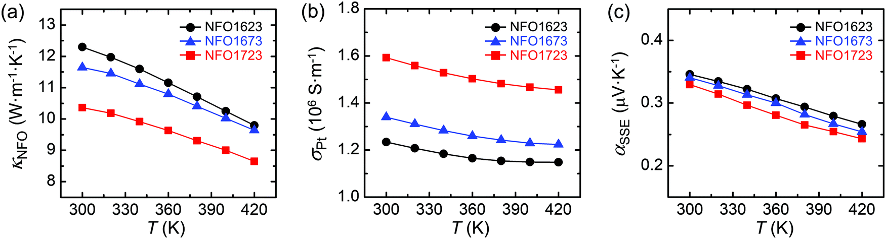 | ||
| Fig. 2 Comparison of temperature dependence of (a) thermal conductivity κNFO of polycrystalline NiFe2O4 (NFO) samples, (b) electrical conductivity σPt of Pt layer, and (c) spin Seebeck coefficient αSSE of polycrystalline NFO/Pt samples (NFO1623, 1673 and 1723 – sintered at 1623, 1673 and 1723 K, respectively). | ||
Microstructure and composition of NFO
To understand underlying mechanisms for the thermoelectric properties of our samples (Fig. 2), we first explored microstructure and composition of NFO samples using the FE-SEM, SEM-EDS, and STEM characterizations. The fabricated NFO samples contain many precipitates in the matrix (Fig. 3a and Fig. S5 in ESI†), and their size increases from 4.2 μm to 9.5 μm with the sintering temperature (Fig. 3b). The Ni/Fe ratio of the precipitates roughly increases (red triangles in Fig. 3c) while the ratio of the NFO matrix slightly decreases from 0.487 to 0.482 with the sintering temperature (grey circles in Fig. 3c). These results support that a large amount of Ni-rich precipitates (including a small amount of Fe) were formed in the NFO matrix during the high-temperature sintering process. The STEM observation (see below for details) reveals that the precipitates possess rock-salt (wüstite) structure, indicating a Ni-rich monoxide phase was formed in the NFO matrix. So, we henceforth designate these Ni-rich monoxide phases as Fe-doped NiO. As described above, the amount of Fe-doped NiO precipitates increases with the sintering temperature, and this increase gives rise to a decrease in mass magnetization (Fig. S6 in ESI†) due to the increased amount of very weak ferromagnetic Fe-doped NiO40 in the NFO matrix.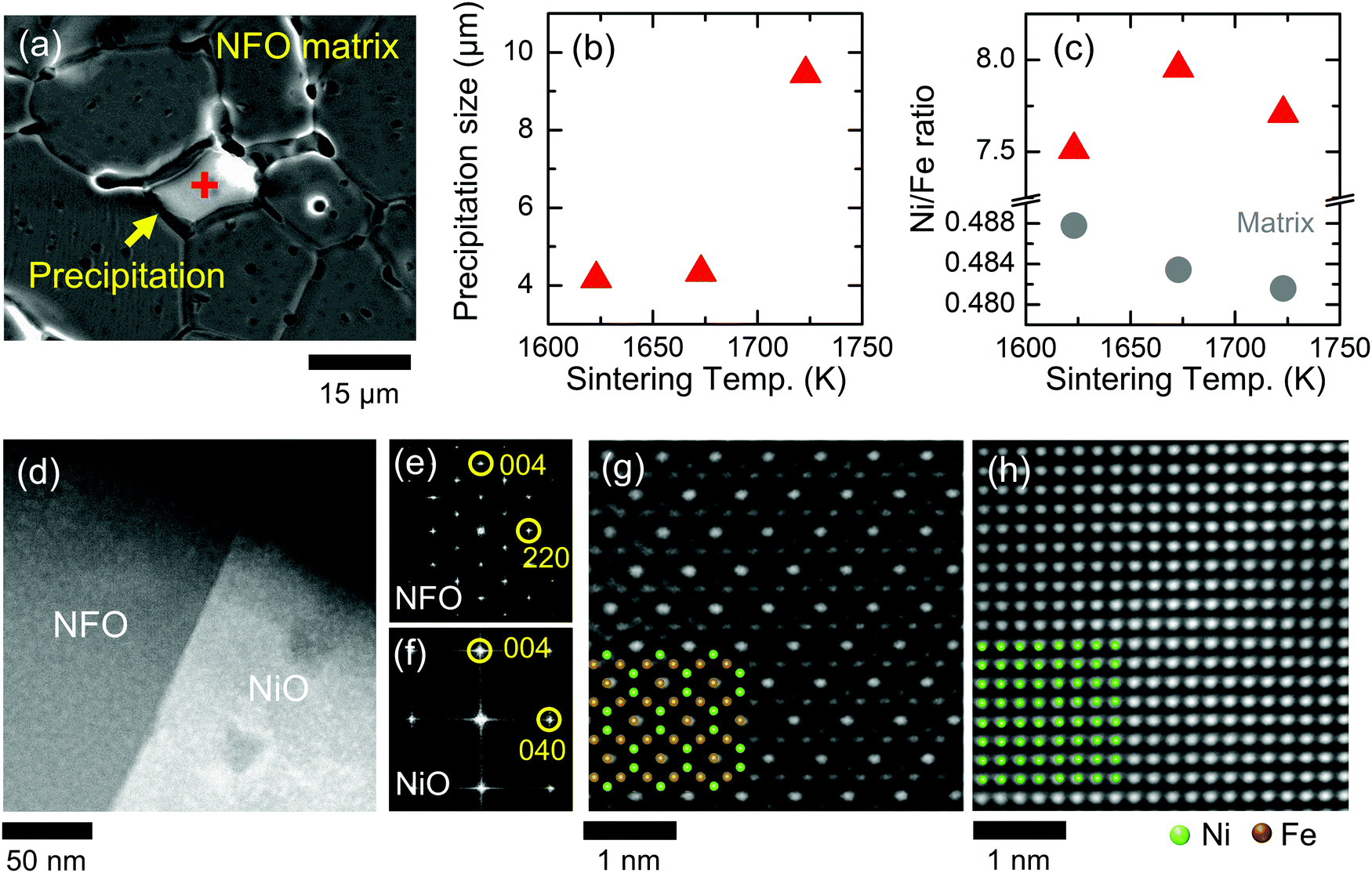 | ||
| Fig. 3 Microstructure and composition analysis of NFO matrix/Fe-doped NiO precipitates of NFO1723. (a) FE-SEM image of the NFO matrix and NiO precipitation. (b) Size distribution of NiO precipitates. (c) Ni/Fe ratio of the NiO precipitates (red triangles) and NFO matrix (grey circles). (d) Cross-sectional HAADF-STEM image and (e and f) FFT patterns on a near-interface region between the (e) NFO matrix and (f) NiO precipitation. (g and h) Atomic resolution HAADF-STEM image of the (g) NFO matrix in [110] orientation and (h) NiO precipitation in [100] orientation. Inset images are simulated STEM-HAADF images on each zone axis. | ||
Detailed microstructure of the mixed NiO and NFO phases was examined by the cross-sectional STEM observation. The observation site is a near-interface region (Fig. 3d) between the Fe-doped NiO precipitate and the NFO matrix of NFO1723 because it has the lowest κNFO. The fast Fourier transform (FFT) patterns (Fig. 3e and f) and the atomic resolution high-angle annular dark-field (HAADF)-STEM images (Fig. 3g and h) clearly identify the spinel structure of NFO matrix and the rock-salt (wüstite) structure of Fe-doped NiO precipitate. Chemical composition analysis using the STEM-EDS shows that the NFO matrix has Ni-deficient compositions of Ni1−δFe2O4 while the Fe-doped NiO precipitate has Ni-rich composition (Fig. S7 and Table S1 in ESI†). The monoxide Fe-doped NiO could be induced in the NFO matrix due to the high temperature (>1473 K) sintering by referring to the Ni–Fe–O2 phase diagram41 (Fig. S2 in ESI†). The oxygen vacancy generation in NFO at elevated temperatures and charge neutrality requirement could be a major driving force to form the rock-salt Fe-doped NiO, wherein the average oxidation number of cations is lower than that in the spinel NFO.
Next, we also observed the detailed microstructure inside the Fe-doped NiO precipitate. Interestingly, the HAADF-STEM images of NFO1723 (Fig. 4a and b) show that many square nano-precipitates with different size (up to tens of nanometers) are uniformly distributed inside the Fe-doped NiO precipitate. The phase of nano-precipitates is clearly identified as the spinel structure, which was estimated from the difference in superlattice reflections of the corresponding FFT patterns (marked as red circles in insets of Fig. 4b). The spinel nano-precipitates are also distinguished from the rock-salt NiO precipitate by colored inverse FFT image (Fig. S8 in ESI†). Chemical composition of the nano-precipitates, i.e., the ratio of Ni, Fe and O counts, is similar to those of NFO matrix (Table S1 in ESI†). So, we can conclude that the nano-sized NFO precipitates were generated in the Fe-doped NiO precipitate during the sintering process. This result is in accordance with the previous report about precipitation of nano-sized NFO from 4 at% Fe-doped NiO material after cooling (100 °C h−1) it from above solvus temperature of 1473 K.42 Thus, the observation thus far suggests that our NFO samples possess an intriguing hierarchical microstructure of NFO matrix – micro-sized Fe-doped NiO precipitates – nano-sized NFO precipitates.
 | ||
| Fig. 4 Microstructure analysis inside Fe-doped NiO precipitate. (a) Low-magnification of HAADF-STEM image of a near-edge region of the NiO precipitate along [100] zone axis. The dark spots correspond to nano-sized NFO precipitates. (b) Nano-sized NFO precipitate embedded in the micro-sized NiO precipitate. The insets are FFT patterns of region 1 and 2. (c) High resolution HAADF-STEM image of the micro-NiO/nano-NFO interface. (d) Enlarged region of the micro-NiO/nano-NFO interface. Yellow dashed circles indicate Ni/Fe disorder region. | ||
An interface region (Fig. 4c) between the nano-NFO and its surrounding Fe-doped NiO was magnified (Fig. 4d) for close examination of strain between the two phases; Ni and Fe ions are indicated by green and brown circles. Lattice of the two phases appears to be well aligned in the same crystal direction. A 1 to 2 unit-cell region (yellow dashed circles) of the intermixed Ni and Fe ions only exists at the nano-NFO/micro-NiO interface. Accordingly, no significant effect of the strain was observed at the interface from high-resolution strain mapping image (Fig. S9 in ESI†).
Discussion on the thermal conductivity reduction
The widespread micro-NiO and embedded nano-NFO precipitates can effectively suppress heat conduction in the NFO samples by scattering phonons, leading to the reduction of κNFO observed in Fig. 2a. Here, we assume that phonons dominantly contribute to the heat transport because our NFO samples are electrically insulating. Although magnons conduct heat as well, their contribution is usually negligible at 300 K and above,43 the temperature range under consideration in this work. The influence of the precipitates on κNFO can be closely examined by the phonon Boltzmann transport approach, where lattice thermal conductivity κL is expressed as a function of phonon frequency ω such that44 | (2) |
| τtot−1(ω) = τu−1(ω) + τnp−1(ω) + τb−1. | (3) |
First, the Umklapp contribution is described by45,46
 | (4) |
 | (5) |
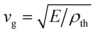 by the Debye theory44 where E is the Young's modulus and ρth is the theoretical density of solid. With E = 99.4 GPa49 and ρth = 5.368 g cm−3 for NFO, we find vg = 4303 m s−1. Plugging those γ and vg values with ma = 234.38 g mol−1
![[thin space (1/6-em)]](https://www.rsc.org/images/entities/char_2009.gif) 34 into eqn (5) yields φ = 9.03 × 10⁻¹⁷ s. Our experimental fit to the measured κNFO for the three NFO samples gives the φ values that are close to each other (Table 1), suggesting the lattice anharmonicity is similar between them. The average φavg = 1.11 × 10⁻¹⁶ s also agrees with the above theoretical value φ = 9.03 × 10⁻¹⁷ s within 20%; this agreement supports that our experimental fitting procedure provides reliable estimates of φ as well as τu−1 and τnp−1 (see below for details).
34 into eqn (5) yields φ = 9.03 × 10⁻¹⁷ s. Our experimental fit to the measured κNFO for the three NFO samples gives the φ values that are close to each other (Table 1), suggesting the lattice anharmonicity is similar between them. The average φavg = 1.11 × 10⁻¹⁶ s also agrees with the above theoretical value φ = 9.03 × 10⁻¹⁷ s within 20%; this agreement supports that our experimental fitting procedure provides reliable estimates of φ as well as τu−1 and τnp−1 (see below for details).
| κ NFO (W m−1 K−1) | φ (s) | τ u −1(s−1) | τ np −1 (s−1) | τ b −1 (s−1) | τ np −1/τtot−1 | |
|---|---|---|---|---|---|---|
| NFO1623 | 12.3 | 1.12 × 10⁻¹⁶ | 1.02 × 10⁹ | 4.90 × 10⁹ | 3.22 × 10⁸ | 0.78 |
| NFO1673 | 11.6 | 1.06 × 10⁻¹⁶ | 9.70 × 10⁸ | 4.95 × 10⁹ | 2.28 × 10⁸ | 0.80 |
| NFO1723 | 10.4 | 1.16 × 10⁻¹⁶ | 1.06 × 10⁹ | 5.51 × 10⁹ | 2.20 × 10⁸ | 0.81 |
The nano-precipitates contribution is described by50,51
| τnp−1 = vgθN, | (6) |
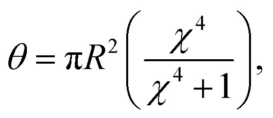 | (7) |
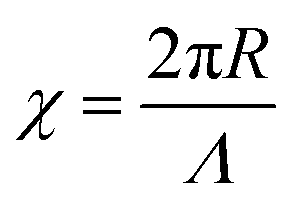 | (8) |
Effect of the grain size on κL can be evaluated by τb−1 = vg/L (L: grain size).54,55 The grain size distribution shows that the average grain size gradually increases from 13.8 μm to 23.0 μm with the sintering temperature (Fig. S10 in ESI†). These numbers are far larger than the mean free path of phonons at 300 K;56,57 therefore, not much contribution of τb−1 is expected. In addition, although the larger grain size of NFO1723 is still expected to lead to higher κL, the lowest κL of NFO 1723 among the three samples suggests that the other scattering mechanisms mentioned above play more dominant roles in the phonon scattering. Concerning the micro-NiO precipitates, as their size is a few μm in all three samples (Fig. 3b), we may presume that those micro-sized precipitates behave such as the grains in matrix. Therefore, likewise a relatively small contribution to phonon scattering is expected.
By fitting the experimental κNFO data in Fig. 2a with the theoretical estimation derived from eqn (2) (see Section VII in ESI†), we can quantitatively evaluate τu−1, τnp−1 and τb−1, and compare the relative contribution of each scattering mechanism to the phonon scattering. The estimated τu−1, τnp−1, τb−1 and τnp−1/τtot−1 for each sample are summarized in Table 1. It is noted that the contribution of nano-NFO precipitates, τnp−1, turns out to be the most dominant in all three samples, whereas that of grain boundary, τb−1, is one order of magnitude smaller than the other two mechanisms as predicted above. In-between three samples, τnp−1 clearly shows an increasing behavior as the sintering temperature rises, due to the associated growth of R and N of the nano-precipitates. As for τu−1, no clear trend is observed between the samples, suggesting that the degree of phonon anharmonicity is comparable in all samples. Finally, the relative change of τnp−1/τtot−1 agrees well with that of κNFO between the three samples. With the phonon scattering analysis thus far, we may summarize that the phonon heat transport in our NFO samples is dominantly affected by the presence of nano-NFO precipitates, and the observed significant reduction of κNFO for the NFO1723 sample can be explained by its larger size (R) and higher number density (N) of the nano-NFO precipitates than the other samples.
Surface characteristics of NFO and electrical conductivity of Pt
We examined the surface morphological characteristics of each sample before the Pt deposition with the BSE and AFM images (Fig. 5). The deliberately controlled surfaces have the uniformly distributed pores with a size of several micrometers (Fig. 5a–c). Among the three samples, NFO1723 has the most compact surface (Fig. 5c), which can be attributed to its highest sintering temperature of 1723 K that easily facilitated heat diffusion between NFO precursor powder during the sintering process. The pore characteristics on the surface was quantitatively evaluated by measuring the pore area fraction in 100 μm × 100 μm area for each sample, which helped to quantify inactive regime for spin pumping. The active area fraction, obtained by 100 − pore area fraction (%), gradually increases with the sintering temperature (Fig. 5d); this result agrees well with the bulk relative density change of each ranging from 93.3% (NFO1623) to 95.6% (NFO1723). As for the average surface roughness analysis (Fig. 5e–g), we limited our AFM measurements to 2 μm × 2 μm area wherein no pores existed. So, only nanoscale scratches on the surface were included while excluding large-scale defect structures from evaluating the surface roughness. The average surface roughness of all samples falls within the range of 0.55 nm (NFO1723) to 0.79 nm (NFO1623) (Fig. 5h). This range is enough to drive efficient spin pumping at the FM/NM interface, as previously reported.29,31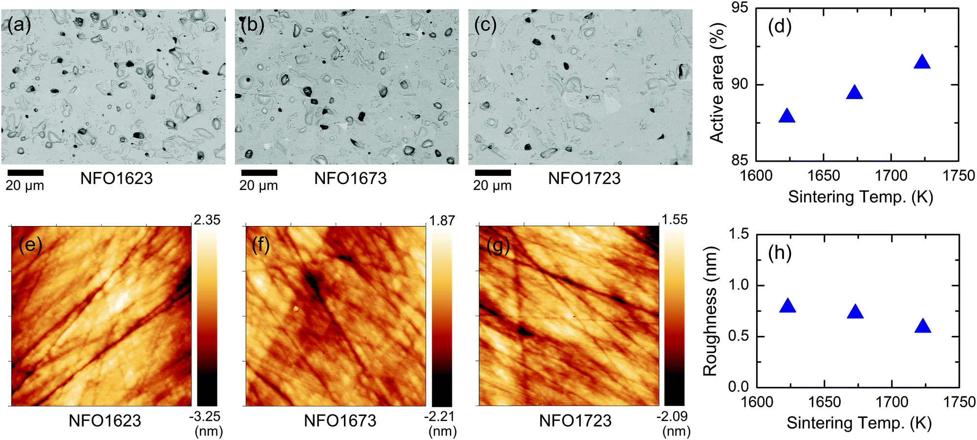 | ||
| Fig. 5 Surface morphological characteristics analysis before Pt deposition. (a–c) BSE images of (a) NFO1623, (b) NFO1673, and (c) NFO1723. (d) Active area fraction versus sintering temperature. (e–g) AFM images of (e) NFO1623, (f) NFO1673, and (g) NFO1723. (h) Average surface roughness versus sintering temperature. | ||
The varying porosity and surface roughness can largely alter σPt of the deposited 10 nm-thick Pt layer because the interface morphology condition influences the quality of Pt growth. Generally, surface with small porosity and roughness leads to high σPt due to suppressed electron scattering in the Pt layer.58–60 For our NFO/Pt samples, the increased sintering temperature results in the reduced porosity and surface roughness; thus, we expect σPt to be increased with the sintering temperature, which was experimentally confirmed in Fig. 2b.
Analysis of the spin Seebeck coefficient
Now we turn our attention to the analysis of αSSE. It is known that αSSE is determined by multiple parameters, which can be categorized into three different groups according to each of relevant physical domains. The first domain is the NM layer wherein the ISHE-induced electrical field EISHE under a given ∇Tz leads to the experimentally estimated αSSE as16αSSE = |![[E with combining right harpoon above (vector)]](https://www.rsc.org/images/entities/i_char_0045_20d1.gif) ISHE/∇Tz| = |(θSHρNM)ŝ × ( ISHE/∇Tz| = |(θSHρNM)ŝ × (![[j with combining right harpoon above (vector)]](https://www.rsc.org/images/entities/i_char_006a_20d1.gif) s/∇Tz)|, s/∇Tz)|, | (9) |
s are the unit vector along electron-spin polarization in the NM layer and the spatial direction of spin current (with the magnitude of spin current density js) induced by SSE, respectively. The second domain is the FM/NM interface where the spin pumping occurs. The efficiency of spin pumping determines js pumped into the NM layer and in turn affects αSSE as given in eqn (9). The last domain corresponds to the FM layer wherein the magnon current is generated by ∇Tz and propagates to the FM/NM interface. It has been shown19,61 that the estimated αSSE in YIG/Pt system is proportional to the amount of magnon accumulation at the interface. In the following discussion, we attempt to interpret the observed trend of αSSE among the three NFO samples. We do so by correlating the surface and bulk property changes with relevant parameters that affect αSSE.
First, we discuss how the surface morphology-induced change in σPt influences αSSE through the rewritten eqn (9) as follows:62–64
 | (10) |
 . For our three NFO samples, we calculated
  using θSH = (1600 Ω−1 cm−1)/σPt, ρNM = ρPt = 1/σPt, λNM = (0.61 × 10⁻¹⁵ Ωm2) × σPt,65,66 and dNM = 10 nm. The estimated
  decreases as the sintering temperature increases (Fig. 6a) mostly due to the increased σPt. This result suggests that the improved surface morphology by the high-temperature sintering leads to the diminished Pt contribution to αSSE. Although not investigated in the current work, it is worth to note that the optimization of dNM is also important as it can influence both αSSE and σNM.30
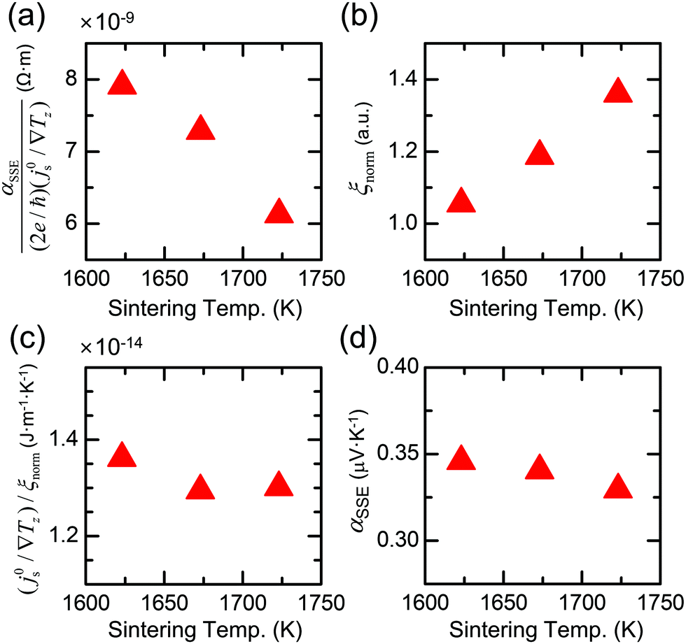 | ||
Fig. 6 (a)  representing the ISHE efficiency of Pt layer at 300 K. (b) Spin pumping efficiency ξnorm of the NFO/Pt interface at 300 K. (c) (j0s/∇Tz)/ξnorm representing bulk magnon contribution to αSSE at 300 K. (d) Experimentally determined spin Seebeck coefficient αSSE of the NFO/Pt system at 300 K. representing the ISHE efficiency of Pt layer at 300 K. (b) Spin pumping efficiency ξnorm of the NFO/Pt interface at 300 K. (c) (j0s/∇Tz)/ξnorm representing bulk magnon contribution to αSSE at 300 K. (d) Experimentally determined spin Seebeck coefficient αSSE of the NFO/Pt system at 300 K. | ||
Next, to examine how the varying surface characteristics affect the spin pumping efficiency at the FM/NM interface, we introduce a new dimensionless parameter ξnorm that represents qualitative spin pumping efficiency accounted by the interface morphology condition. By referring to our previous work,31 we can infer that ξnorm is linearly proportional to the active area fraction of NFO surface, regardless of the change in surface roughness (see Fig. S11 in ESI† for details). For our current samples, the active area fraction increases with the sintering temperature with little variance in the surface roughness; thus, we can estimate that ξnorm at 300 K accordingly increases from 1.06 (NFO1623) to 1.36 (NFO1723) (Fig. 6b). This result indicates that the latter sample has the highest spin pumping efficiency due to its largest active area fraction.
Lastly, how much magnons accumulate at the FM/NM interface in the bulk FM largely determines the pumped magnon current density j0s/∇Tz and thus αSSE. It has been shown19,61,67 that such magnon accumulation at the interface induces temperature difference between magnons in FM and electrons in NM, and the difference works as driving force for spin pumping across the interface with the spin pumping efficiency ξnorm. Thus, j0s/∇Tz reflects the combined contribution of both bulk FM and FM/NM interface; j0s/∇Tz is proportional to the magnon accumulation in the FM and ξnorm at the FM/NM interface. Therefore, the normalized (j0s/∇Tz)/ξnorm is necessary to qualitatively account for the sole contribution of bulk magnons in FM to j0s/∇Tz by excluding the contribution of ξnorm. For our NFO samples, (j0s/∇Tz)/ξnorm hardly changes with the sintering temperature (Fig. 6c), suggesting similar degrees of magnon accumulation at the interface of all three samples. This result is quite intriguing, considering that the phonon contribution to κNFO is significantly suppressed in the NFO samples that were sintered at higher temperature. It suggests that the nano-NFO precipitates, which work as the dominant scatterers for heat-carrying phonons, barely affect the magnon transport that contributes to SSE. This discrepancy can be understood by comparing the relevant length scales of phonons and magnons, and the relative effects of nano-NFO precipitates on each transport as below.
Our detailed analysis on the phonon heat transport given above reveals that the nano-NFO precipitates mostly scatter the phonons in the short-wavelength limit at 300 K. As for magnon scattering, the nano-NFO precipitates are likely to work in the same way as they do for the phonons; only the short-wavelength limit is relevant, because their magnetic and lattice properties are identical with those of the matrix, making θ → 0 in the long-wavelength limit. This means that the nano-precipitates likewise preferentially scatter short-wavelength magnons; the intensity of scattering for them should vary between the samples with the different nano-NFO contents. In that sense, the observed negligible variation in the magnon contribution to αSSE (Fig. 6c) strongly suggests that the magnons, other than those in the short-wavelength regime, are barely scattered by the nano-precipitates and may play a dominant role in inducing SSE. In the case of YIG/Pt system, there is an increasing consensus that SSE at 300 K is mediated primarily by sub-thermal magnons with the energies below ∼40 K and corresponding long-wavelengths.18,43,68 Our observation indicates that the SSE in NFO/Pt may also be largely driven by the similarly long-wavelength magnons to those in YIG. On the other hand, we do not exclude the possibility that the scattering of short-wavelength magnons by nano-precipitates is not spin-flipping in its nature, so that the short-wavelength magnons make a considerable contribution to SSE in NFO/Pt. Further experimental study such as low temperature and high magnetic field measurements of SSE could provide more detailed information regarding the relevant energy and wavelength of magnons in NFO.18,20 Other than the nano-NFO precipitates, another possible mechanism for the magnon scattering is the grain boundary scattering. It has been shown24 that the relevant propagation length scale of magnons, that determines αSSE, is the spin diffusion length in bulk FM, while the magnon energy relaxation length can play an important role in the case of thin films. The spin diffusion length of thermally excited magnons in NFO has been reported to be 2 to 3 μm at 300 K.69,70 Since the average grain size of our NFO samples ranges between 13.8 μm and 23.0 μm, much larger than the spin diffusion length of NFO, no significant scattering of magnons off the grain boundaries is expected as in the case of phonons.
In addition, it has been suggested that the magnon propagation characteristics can be estimated by referring to the critical exponents of temperature dependence of SSE.23,71 The critical exponents for the three NFO samples were calculated by fitting the temperature dependence of (j0s/∇Tz)/ξnorm (see ESI† for details), which reveal that all samples show comparable critical exponent values. This result supports that the magnon propagation in our NFO samples is hardly affected by the presence of nano-precipitates or grain boundaries.
Now we can understand the observed trend in αSSE in the three NFO samples at 300 K (Fig. 6d) by considering the above discussed three contributions. The Pt contribution 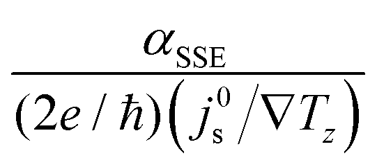 and the spin pumping efficiency (ξnorm) show their compensating dependences on the sintering temperature. In contrast, the bulk magnon contribution (j0s/∇Tz)/ξnorm barely changes with the sintering temperature. As a result, αSSE exhibits very small variation between the three samples, proving its robustness against the scattering mechanisms that significantly suppress κNFO.
Conclusions
We demonstrate a facile approach to simultaneously optimize the bulk FM and FM/NM interface for ZSSET improvement. Experimentally, the approach is executed at ease by simply adjusting the heat treatment conditions of the polycrystalline NFO/Pt platform. The resulting phase separation in NFO matrix enables the controlled generation of distinctive hierarchical microstructure within the bulk NFO. The nano-precipitates in the hierarchical microstructure selectively scatter heat carrying phonons while barely affecting magnons, making the bulk NFO a phonon-glass magnon-crystal system with an improved αSSE2/κFM. In-depth analyses of experimentally measured κFM and αSSE reveal that the different impacts that the nano-precipitates have on phonons and magnons may originate from the large discrepancy in the relevant length scales in the two systems. Such a phonon-glass magnon-crystal concept can also be useful for realizing a high-performance spin Peltier device, since SSE and the spin Peltier effect are conjugated by the Onsager reciprocal relation.72,73 We also show that the simple heat treatments simultaneously lead to clean and smooth NFO/Pt interfaces. The well-controlled interface morphology enables efficient spin pumping at the interface as well as high-quality growth of the Pt layer, which results in an improved αSSE2σNM. Our study provides an efficient way to increase the thermoelectric efficiency of SSE by combining proper heat treatments and temperature-dependent phase separation in oxide systems. The proposed approach may be applied to various oxide-based SSE structures and contribute to designing highly efficient transverse thermoelectric devices.Author contributions
M. Y. Kim: methodology, validation, formal analysis, investigation, writing – original draft preparation, writing – review & editing, S. J. Park: methodology, validation, writing – review & editing, G.-Y. Kim: formal analysis, investigation, writing – review & editing, S.-Y. Choi: formal analysis, funding acquisition, investigation, supervision, writing – review & editing, H. Jin: conceptualization, funding acquisition, methodology, supervision, writing – review & editing.Conflicts of interest
There are no conflicts to declare.Acknowledgements
M. Y. K., S. J. P. and H. J. acknowledge the support of the National Research Foundation of Korea (NRF) grant funded by the Korea government (MSIT) (NRF-2020R1C1C100429112) and the Ministry of Education, Science and Technology (NRF-2020K1A4A7A0209543811). G.-Y. K. and S.-Y. C. acknowledge the support of the Global Frontier Hybrid Interface Materials of the National Research Foundation of Korea (NRF) funded by the Ministry of Science and ICT (2013M3A6B1078872), and Korea Basic Science Institute (National research Facilities and Equipment Center) Grant (2020R1A6C101A202) funded by the Ministry of Education.References
- Global Energy and CO2 Status Report 2019, https://www.iea.org/reports/global-energy-co2-status-report-2019, (accessed February, 2021).
- F. J. DiSalvo, Science, 1999, 285, 703–706 CrossRef CAS.
- L. E. Bell, Science, 2008, 321, 1457–1461 CrossRef CAS.
- M. S. Dresselhaus, G. Chen, M. Y. Tang, R. G. Yang, H. Lee, D. Z. Wang, Z. F. Ren, J. P. Fleurial and P. Gogna, Adv. Mater., 2007, 19, 1043–1053 CrossRef CAS.
- G. J. Snyder and E. S. Toberer, Nat. Mater., 2008, 7, 105–114 CrossRef CAS.
- S. R. Boona, K. Vandaele, I. N. Boona, D. W. McComb and J. P. Heremans, Nat. Commun., 2016, 7, 13714 CrossRef CAS.
- M. Mizuguchi and S. Nakatsuji, Sci. Technol. Adv. Mater., 2019, 20, 262–275 CrossRef CAS.
- W. Zhou, K. Yamamoto, A. Miura, R. Iguchi, Y. Miura, K. Uchida and Y. Sakuraba, Nat. Mater., 2021, 20, 463–467, DOI:10.1038/s41563-020-00884-2.
- K. Uchida, S. Takahashi, K. Harii, J. Ieda, W. Koshibae, K. Ando, S. Maekawa and E. Saitoh, Nature, 2008, 455, 778–781 CrossRef CAS PubMed.
- C. M. Jaworski, J. Yang, S. Mack, D. D. Awschalom, J. P. Heremans and R. C. Myers, Nat. Mater., 2010, 9, 898–903 CrossRef CAS PubMed.
- K. Uchida, H. Adachi, T. Ota, H. Nakayama, S. Maekawa and E. Saitoh, Appl. Phys. Lett., 2010, 97, 172505 CrossRef.
- K. Uchida, J. Xiao, H. Adachi, J. Ohe, S. Takahashi, J. Ieda, T. Ota, Y. Kajiwara, H. Umezawa, H. Kawai, G. E. W. Bauer, S. Maekawa and E. Saitoh, Nat. Mater., 2010, 9, 894–897 CrossRef CAS PubMed.
- G. E. W. Bauer, E. Saitoh and B. J. van Wees, Nat. Mater., 2012, 11, 391–399 CrossRef CAS PubMed.
- S. R. Boona, R. C. Myers and J. P. Heremans, Energy Environ. Sci., 2014, 7, 885–910 RSC.
- S. R. Boona, S. J. Watzman and J. P. Heremans, APL Mater., 2016, 4, 104502 CrossRef.
- K. Uchida, H. Adachi, T. Kikkawa, A. Kirihara, M. Ishida, S. Yorozu, S. Maekawa and E. Saitoh, Proc. IEEE, 2016, 104, 1946–1973 CAS.
- E. Saitoh, M. Ueda, H. Miyajima and G. Tatara, Appl. Phys. Lett., 2006, 88, 182509 CrossRef.
- H. Jin, S. R. Boona, Z. Yang, R. C. Myers and J. P. Heremans, Phys. Rev. B: Condens. Matter Mater. Phys., 2015, 92, 054436 CrossRef.
- A. Kehlberger, U. Ritzmann, D. Hinzke, E. Guo, J. Cramer, G. Jakob, M. C. Onbasli, D. H. Kim, C. A. Ross, M. B. Jungfleisch, B. Hillebrands, U. Nowak and M. Kläui, Phys. Rev. Lett., 2015, 115, 096602 CrossRef PubMed.
- T. Kikkawa, K. Uchida, S. Daimon, Z. Qiu, Y. Shiomi and E. Saitoh, Phys. Rev. B: Condens. Matter Mater. Phys., 2015, 92, 064413 CrossRef.
- E. Guo, J. Cramer, A. Kehlberger, C. A. Ferguson, D. A. MacLaren, G. Jakob and M. Kläui, Phys. Rev. X, 2016, 6, 031012 Search PubMed.
- S. M. Rezende, R. L. Rodríguez-Suárez, R. O. Cunha, J. C. López Ortiz and A. Azevedo, J. Magn. Magn. Mater., 2016, 400, 171–177 CrossRef CAS.
- A. Miura, T. Kikkawa, R. Iguchi, K. Uchida, E. Saitoh and J. Shiomi, Phys. Rev. Mater., 2017, 1, 014601 CrossRef.
- A. Prakash, B. Flebus, J. Brangham, F. Yang, Y. Tserkovnyak and J. P. Heremans, Phys. Rev. B, 2018, 97, 020408 CrossRef CAS.
- B. Poudel, Q. Hao, Y. Ma, Y. Lan, A. Minnich, B. Yu, X. Yan, D. Wang, A. Muto, D. Vashaee, X. Chen, J. Liu, M. S. Dresselhaus, G. Chen and Z. Ren, Science, 2008, 320, 634–638 CrossRef CAS PubMed.
- D. Wu, L. Zhao, S. Hao, Q. Jiang, F. Zheng, J. W. Doak, H. Wu, H. Chi, Y. Gelbstein, C. Uher, C. Wolverton, M. Kanatzidis and J. He, J. Am. Chem. Soc., 2014, 136, 11412–11419 CrossRef CAS PubMed.
- W. Li, L. Zheng, B. Ge, S. Lin, X. Zhang, Z. Chen, Y. Chang and Y. Pei, Adv. Mater., 2017, 29, 1605887 CrossRef PubMed.
- H. Jin and J. P. Heremans, Phys. Rev. Mater., 2018, 2, 115401 CrossRef CAS.
- A. Aqeel, I. J. Vera-Marun, B. J. van Wees and T. T. M. Palstra, J. Appl. Phys., 2014, 116, 153705 CrossRef.
- Y. Saiga, K. Mizunuma, Y. Kono, J. C. Ryu, H. Ono, M. Kohda and E. Okuno, Appl. Phys. Express, 2014, 7, 093001 CrossRef CAS.
- M. Kim, S. J. Park and H. Jin, J. Appl. Phys., 2020, 127, 085105 CrossRef CAS.
- A. T. Nelson, J. T. White, D. A. Andersson, J. A. Aguiar, K. J. McClellan, D. D. Byler, M. P. Short and C. R. Stanek, J. Am. Ceram. Soc., 2014, 97, 1559–1565 CrossRef CAS.
- G. A. Slack and S. B. Austerman, J. Appl. Phys., 1971, 42, 4713–4717 CrossRef CAS.
- R. C. Weast, CRC Handbook of Chemistry and Physics, The Chemical Rubber Co., Cleveland, 50th edn, 1969 Search PubMed.
- K. Uchida, T. Nonaka, T. Ota and E. Saitoh, Appl. Phys. Lett., 2010, 97, 262504 CrossRef.
- J. D. Arboleda, O. Arnache Olmos, M. H. Aguirre, R. Ramos, A. Anadon and M. R. Ibarra, Appl. Phys. Lett., 2016, 108, 232401 CrossRef.
- J. D. Arboleda, O. Arnache, M. H. Aguirre, R. Ramos, A. Anadón and M. R. Ibarra, Solid State Commun., 2018, 270, 140–146 CrossRef CAS.
- D. Meier, T. Kuschel, L. Shen, A. Gupta, T. Kikkawa, K. Uchida, E. Saitoh, J. M. Schmalhorst and G. Reiss, Phys. Rev. B: Condens. Matter Mater. Phys., 2013, 87, 054421 CrossRef.
- D. Meier, D. Reinhardt, M. van Straaten, C. Klewe, M. Althammer, M. Schreier, S. T. B. Goennenwein, A. Gupta, M. Schmid, C. H. Back, J. M. Schmalhorst, T. Kuschel and G. Reiss, Nat. Commun., 2015, 6, 8211 CrossRef CAS PubMed.
- R. Krishnakanth, G. Jayakumar, A. Albert Irudayaraj and A. Dhayal Raj, Mater. Today: Proc., 2016, 3, 1370–1377 Search PubMed.
- The phase diagram of Fe-Ni-O2 in air, https://www.crct.polymtl.ca/fact/phase_diagram.php?file=Fe-Ni-O_Fe-Ni-O2_air.jpg&dir=FToxid, (accessed February, 2021).
- S. R. Summerfelt and C. B. Carter, J. Am. Ceram. Soc., 1992, 75, 2244–2250 CrossRef CAS.
- S. R. Boona and J. P. Heremans, Phys. Rev. B: Condens. Matter Mater. Phys., 2014, 90, 064421 CrossRef CAS.
- N. W. Ashcroft and N. D. Mermin, Solid State Physics, Cengage Learning, Belmont, 1976 Search PubMed.
- G. A. Slack and S. Galginaitis, Phys. Rev., 1964, 133, A253–A268 CrossRef.
- D. T. Morelli, J. P. Heremans and G. A. Slack, Phys. Rev. B: Condens. Matter Mater. Phys., 2002, 66, 195304 CrossRef.
- N. L. Vočadlo and G. D. Price, Phys. Earth Planet. Inter., 1994, 82, 261–270 CrossRef.
- H. Perron, T. Mellier, C. Domain, J. Roques, E. Simoni, R. Drot and H. Catalette, J. Phys.: Condens. Matter, 2007, 19, 346219 CrossRef.
- P. Chavan, L. R. Naik, P. B. Belavi, G. Chavan, C. K. Ramesha and R. K. Kotnala, J. Electron. Mater., 2017, 46, 188–198 CrossRef CAS.
- A. Majumdar, J. Heat Transfer, 1993, 115, 7–16 CrossRef.
- W. Kim and A. Majumdar, J. Appl. Phys., 2006, 99, 084306 CrossRef.
- X. Yang, J. Carrete and Z. Wang, J. Appl. Phys., 2015, 118, 085701 CrossRef.
- Z. Wang, X. Yang, D. Feng, H. Wu, J. Carrete, L. Zhao, C. Li, S. Cheng, B. Peng, G. Yang and J. He, ACS Appl. Mater. Interfaces, 2017, 9, 3686–3693 CrossRef CAS.
- H. J. Goldsmid and A. W. Penn, Phys. Lett. A, 1968, 27, 523–524 CrossRef CAS.
- J. E. Parrott, J. Phys. C: Solid State Phys., 1969, 2, 147–151 CrossRef.
- D. Aketo, T. Shiga and J. Shiomi, Appl. Phys. Lett., 2014, 105, 131901 CrossRef.
- Y. Xiao and L. Zhao, npj Quantum Mater., 2018, 3, 55 CrossRef.
- W. D. Westwood, J. Vac. Sci. Technol., 1974, 11, 466–471 CrossRef CAS.
- H. Marom and M. Eizenberg, J. Appl. Phys., 2006, 99, 123705 CrossRef.
- J. S. Agustsson, U. B. Arnalds, A. S. Ingason, K. B. Gylfason, K. Johnsen, S. Olafsson and J. T. Gudmundsson, J. Phys.: Conf. Ser., 2008, 100, 082006 CrossRef.
- S. Hoffman, K. Sato and Y. Tserkovnyak, Phys. Rev. B: Condens. Matter Mater. Phys., 2013, 88, 064408 CrossRef.
- K. Ando, S. Takahashi, J. Ieda, Y. Kajiwara, H. Nakayama, T. Yoshino, K. Harii, Y. Fujikawa, M. Matsuo, S. Maekawa and E. Saitoh, J. Appl. Phys., 2011, 109, 103913 CrossRef.
- H. Nakayama, K. Ando, K. Harii, T. Yoshino, R. Takahashi, Y. Kajiwara, K. Uchida, Y. Fujikawa and E. Saitoh, Phys. Rev. B: Condens. Matter Mater. Phys., 2012, 85, 144408 CrossRef.
- Z. Qiu, K. Ando, K. Uchida, Y. Kajiwara, R. Takahashi, H. Nakayama, T. An, Y. Fujikawa and E. Saitoh, Appl. Phys. Lett., 2013, 103, 092404 CrossRef.
- L. Wang, R. J. H. Wesselink, Y. Liu, Z. Yuan, K. Xia and P. J. Kelly, Phys. Rev. Lett., 2016, 116, 196602 CrossRef PubMed.
- E. Sagasta, Y. Omori, M. Isasa, M. Gradhand, L. E. Hueso, Y. Niimi, Y. Otani and F. Casanova, Phys. Rev. B, 2016, 94, 060412 CrossRef.
- J. Xiao, G. E. W. Bauer, K. Uchida, E. Saitoh and S. Maekawa, Phys. Rev. B: Condens. Matter Mater. Phys., 2010, 81, 214418 CrossRef.
- K. S. Tikhonov, J. Sinova and A. M. Finkel'stein, Nat. Commun., 2013, 4, 1945 CrossRef PubMed.
- J. Shan, P. Bougiatioti, L. Liang, G. Reiss, T. Kuschel and B. J. van Wees, Appl. Phys. Lett., 2017, 110, 132406 CrossRef.
- J. Shan, A. V. Singh, L. Liang, L. J. Cornelissen, Z. Galazka, A. Gupta, B. J. van Wees and T. Kuschel, Appl. Phys. Lett., 2018, 113, 162403 CrossRef.
- K. Uchida, T. Kikkawa, A. Miura, J. Shiomi and E. Saitoh, Phys. Rev. X, 2014, 4, 041023 CAS.
- J. Flipse, F. K. Dejene, D. Wagenaar, G. E. W. Bauer, J. B. Youssef and B. J. van Wees, Phys. Rev. Lett., 2014, 113, 027601 CrossRef CAS PubMed.
- S. Daimon, R. Iguchi, T. Hioki, E. Saitoh and K. Uchida, Nat. Commun., 2016, 7, 13754 CrossRef CAS PubMed.
Footnote |
| † Electronic supplementary information (ESI) available. See DOI: 10.1039/d1ee00667c |
| This journal is © The Royal Society of Chemistry 2021 |