
Epitaxial halide perovskite-based materials for photoelectric energy conversion
Ziren
Zhou
 ,
Hong Wei
Qiao
,
Yu
Hou
*,
Hua Gui
Yang
* and
Shuang
Yang
*
,
Hong Wei
Qiao
,
Yu
Hou
*,
Hua Gui
Yang
* and
Shuang
Yang
*
Key Laboratory for Ultrafine Materials of Ministry of Education, Shanghai Engineering Research Center of Hierarchical Nanomaterials, School of Materials Science and Engineering, East China University of Science and Technology, Shanghai 200237, China. E-mail: yhou@ecust.edu.cn; hgyang@ecust.edu.cn; syang@ecust.edu.cn
First published on 3rd November 2020
Abstract
Metal halide perovskites (MHP) are an emerging class of semiconducting materials with superior optoelectronic properties, which have achieved notable success in photoelectric device applications. As a classical technique in the semiconductor industry, epitaxy has indeed advanced the perovskite technology in the recent years by enabling the material combinations with a coherent interfacial lattice as well as combined complementary functionalities, which are not available in the single-phase constituents. In this review, we start with the basic principles and chemical techniques for the epitaxial growth of MHP-based materials. We summarize the epitaxial structures of perovskite solids, which are categorized by the combined materials and compare their performance in photoelectric devices including solar cells, photodetectors, and light-emitting diodes (LEDs). The impact of lattice strain and band structure at the substrate/perovskite interface, which can affect the energy conversion process, are then discussed after the epitaxial cases. We finally outline the future directions for perovskite epitaxy, targeting the in situ monitoring of the surface atomic kinetics during the growth, precise interfacial structure characterization, and the upscaling fabrications, which might further benefit the performance and application of perovskite-based devices.
 Ziren Zhou | Ziren Zhou received his BS from Xiangtan University in 2017. He is currently a PhD candidate at the East China University of Science and Technology under the supervision of Prof. Hua Gui Yang. His research interest focuses on the design and synthesis of perovskite-related materials for optoelectronics. |
 Yu Hou | Yu Hou completed his BS and PhD from East China University of Science and Technology (ECUST) in 2010 and 2015, respectively. From 2015 to 2017, he worked as a postdoctoral research fellow at ECUST and then joined the Griffith University as a visiting scholar. After finishing his visiting scholar training, he took an associate professor position at ECUST at the end of 2017. His research focuses on novel functional materials of thin film-based solar devices and aims at developing new semiconductor absorbers and cell structures towards next-generation photovoltaic technology. |
 Hua Gui Yang | Hua Gui Yang completed his PhD from the National University of Singapore in 2005. He joined the University of Queensland in 2007 as a postdoctoral research fellow. After finishing his postdoctoral training, he came back to China and took up a professor position at East China University of Science and Technology at the end of 2008. His research interests are focused on the rational design and fabrication of functional materials for solar-energy conversion. |
 Shuang Yang | Shuang Yang received his BS from Tsingtao University of Science and Technology in 2011 and completed his PhD in 2016 from East China University of Science and Technology (ECUST). He then conducted postdoctoral research at Nanyang Technological University and University of Nebraska-Lincoln. Currently, he is a professor at ECUST. His research focuses on the chemistry and physics of semiconducting materials and opto-electrical devices. |
Broader contextEpitaxial technologies have offered a promising avenue for fabricating high-quality, exquisite, and scalable perovskite products with the aim of moving their applications from the lab to the market. The appealing photoelectric energy conversion capabilities provided by epitaxially grown perovskites have stressed the importance of material combinations as well as their detailed epitaxial strategies and methods, which have yet to be systematically summarized as a reference for the scientific community. The rich structural motifs of perovskites, upon homoepitaxy and heteroepitaxy, have greatly expanded their device configurations from multilayer-stacked thin films to miniaturized individual single crystals. Besides, the minimized structural defects benefit from the lattice coherent or vdW gapped interface and the adjustable residual strain level, both of which can profoundly impact the energy conversion performance of perovskite epitaxial structures and their assembled devices. Facilitated by the rapidly developed epitaxial technologies, perovskites are bound to play a more important role in future photonics and electronics, and may break the performance bottleneck of their non-epitaxial counterparts. |
1. Introduction
Despite the prototypical all-inorganic and inorganic–organic hybrid compounds that have been synthesized early in 1893 and 1978,1–3 respectively, the application value of perovskites (defined by the chemical formula of ABX3, where A is a monovalent cation, B is a divalent cation, and X is a halide) as semiconductors was not realized until the recent decades.4–11 Ionic perovskites are accessible from aqueous solutions by the simple adduction of AX and BX2 reagents,4,12–14 and they are compositionally compatible with an increasing diversity of organic and inorganic ionic species.15–23 In a departure from the mainstream IV, III–V, and II–VI semiconductors, perovskites possess many distinguishing features, such as largely tunable direct bandgaps,4,5,12–16,24,25 adjustable quantum well distribution,26–28 anomalous defect tolerance,29–31 and ultralong carrier diffusion length,32,33 which have made them ideal candidates for advanced optoelectronic applications.Similar to conventional semiconductors, the epitaxial assembling of perovskites with other materials is highly feasible and is also appealing for generating combinations with better control on carriers and photons. In 1836, M. L. Frankenheim first artificially reproduced a regular assembly of building blocks between two ionic compounds—a solution-grown parallel oriented sodium nitrate (NaNO3) on a freshly cleaved calcite (CaCO3) crystal,34 which has been regarded as the prototype for contemporary epitaxy. Modern technologies allow similar ionic perovskites to be epitaxially grown with increasingly rich materials through a variety of chemical routes. With the assistance of sophisticated facilities, the atomic adsorption of perovskite at the substrate surface can be carried out down to the monolayer level, which guarantees the accuracy of the layer thickness while at the same time conferring extra benefits on their photoelectrical properties.35,36 Unlike covalent semiconductor thin films whose quality highly relies on the processing conditions and chemical purity, solution-processed perovskite thin films are extremely easy to be prepared, even in ambient air,37–39 and they allow a myriad of foreign additives to further adjust their physicochemical properties.40–44 On the other hand, downscaling the fabrication of individual or dispersed perovskite structures have largely expanded the diversity of perovskite nano-/micro-devices and are expected to overcome the potential limit of their thin film counterparts. For these reasons, abundant opportunities may exist for rationally designing and fabricating compelling perovskite epitaxial structures with wide utilities.
Laboratory-miniaturized perovskite devices have produced fruitful results in a broad range of application fields. As early as 1958, the spectral sensitive photoconductivity of CsPbX3 crystals was first observed to complement its own colors.45 Long after that, in 2009, organic–inorganic hybrid compounds (CH3NH3PbI3/CH3NH3PbBr3) were deposited on n-type TiO2via simple spin-coating and achieved a preliminary power conversion efficiency (PCE) of 3.8% for photovoltaic (PV) cells.4 Since then, more efforts have been devoted to this emerging semiconductor family, accompanied by the discovery of additional physical properties, such as dynamic phase transition,46–50 high dielectric constant,51 giant spin–orbit coupling,52,53 strong structural fluctuations,54,55 and piezo/ferroelectricity.9,10 These uniquely combined properties broaden the perovskites’ applications to photodetectors,7,56–71 LEDs,72–84 lasers,6,85–95 field-effect transistors (FETs),11,96–98 piezo/ferroelectric responsors,99,100etc., more than their currently most successful PV cells.101–122 In these devices that adopt perovskite epitaxial structures as the basic working units, the quality of the perovskite crystals as well their epitaxial interface can originally determine the device performance. It has hence pointed to the necessity of generalizing some common laws over numerous existing cases. Barely involving the concept of epitaxy, previous reviews have given comprehensive retrospect to the fabrication methodology,123–126 crystal formation mechanism,123,124,127 morphological diversity,124,128 and structure–function relationships129,130 of perovskite thin films, nanostructures and colloidal nanocrystals (NCs). With respect to epitaxial homostructures and heterostructures, reviews organized by the material chemistry of substrates (also referred to as hosts here) and the structural plurality of the as-grown perovskites are rare.
In this review, we survey the versatility and feasibility of perovskite solids epitaxially grown with different crystalline materials, including metals, metal halides, V/VI-based materials, van der Waals (vdW) materials, and epitaxial lead compounds for two-step conversion. The detailed epitaxial process of perovskites (including those with colloidal-phase mutual assembly) is presented for each case, in which the growth mechanism and crystallographic affinity are highlighted according to the analytical results. We then gain insights into the relationship between perovskites and substrates, mainly focusing on their adhesion modes and interfacial lattice arrangement. The residual impact from the substrates is set forth by the strain-related properties of the as-grown perovskites beyond epitaxy. Some key factors that might affect the band alignment of the heterostructures are also sorted out to explore the origins of photophysical variations of the perovskites during/after growth. To interpret the significance of epitaxy towards photoelectric energy conversion, specific device applications are introduced right behind each epitaxy case and are further summarized in Tables 1–3. Before delving into the details, we have presented the organization and highlights of this review in Fig. 1. The narration arising from substrate/host materials will center on the structural motifs of perovskite epitaxial structures, and is finally directed to their device or non-device energy conversion applications.
| Device configuration | Method | Absorber structure | V OC (V) | J SC (mA cm−2) | FF (%) | PCEmax (%) (aperture area: cm2) | Ref. |
|---|---|---|---|---|---|---|---|
| Abbreviation: VOC, open-circuit voltage; JSC, short-circuit current; FF, fill factor; PCE, power conversion efficiency; ITO, indium tin oxide; Spiro-OMeTAD, 2,20,7,70-tetrakis[N,N-di(4-methoxyphenyl)amino]-9,90-spirobifluorene; PET, polyethylene terephthalate; SU-8, 1-methoxy-2-propanol acetate; FTO, fluorine-doped tin oxide; c-TiO2, compact-TiO2; m-TiO2, mesoporous-TiO2; AVAI, 5-aminovaleric iodide; PCBM, [6,6]-phenyl-C61-butyric acid methyl ester; VBABr, 4-vinylbenzylammonium bromide; PEDOT:PSS, poly(3,4-ethylenedioxythiophene):poly(styrenesulfonate); FPEAI, 2-(4-fluorophenyl)ethylammonium iodide; BCP, bathocuproine; pF1PEA, 4fluorophenethylammonium; EDT, 1,2-ethanedithol; MZO, MgZnO; PTAA, poly(bis(4-phenyl)(2,4,6-trimethylphenyl)amine); BP, black phosphorene; BPs, black phosphorus; QWs, quantum wells; NA, not available. | |||||||
| ITO/SnO2/FA0.5Cs0.5PbI3/Spiro-OMeTAD/Au | Cation exchange | Heterocrystal | 1.17 | 18.3 | 78.3 | 16.6 (0.058) | 101 |
| PET/ITO/SnO2/MAPb0.5+xSn0.5−xI3/Spiro-OMeTAD/Au/PDMS/SU-8 | Lithography + solution growth + transfer | Single crystalline thin film | NA | NA | NA | 20.0 (0.25)/10.3 (9) | 102 |
| FTO/c-TiO2/m-TiO2/AVAI:MAPbI3/Spiro-OMeTAD/Au | Solution processing | 2D/3D QWs | 1.03 | 18.8 | 75.5 | 14.6 (0.16) | 103 |
| FTO/SnO2/PCBM/BA0.05(FA0.83Cs0.17)0.95Pb(I0.8Br0.2)3/Spiro-OMeTAD/Au | Solution processing | 2D/3D QWs | 1.14 | 22.7 | 80.0 | 20.6 (0.0919) | 104 |
| ITO/TiO2/VBABr:(MA0.95Cs0.05PbBr3)0.15(FA0.95Cs0.05PbI3)0.85/Spiro-OMeTAD/Au | Solution processing | 2D/3D QWs | 1.15 | 22.5 | 78.0 | 20.2 (0.049) | 105 |
| ITO/PEDOT:PSS/FPEAI:(MAPbI3)0.75(FASnI3)0.25/PCBM/BCP/Ag | Solution processing | 2D/3D QWs | 0.79 | 28.4 | 78.0 | 17.5 (0.09) | 106 |
| ITO/NiOx/PEA0.15FA0.85SnI3/PCBM/BCP/Ag | Solution processing | 2D/3D QWs | 0.61 | 22.0 | 70.1 | 9.41 (0.04) | 107 |
| ITO/PEDOT:PSS/(pF1PEA)2MA3Pb4I13/PCBM/Al | Solution processing | 2D/3D QWs | 1.11 | 15.5 | 66.3 | 11.4 (0.13) | 108 |
| FTO/TiO2/SnS@MAPbI3/Spiro-OMeTAD/Au | Ligand exchange | Heterocrystal | 1.04 | 22.7 | 71.6 | 16.8 (NA) | 109 |
| ITO/ZnO/PbS@MAPbI3/PbS-EDT/Au | Ligand exchange | Heterocrystal | 0.61 | 21.8 | 67.9 | 9.0 (0.071) | 110 |
| FTO/c-TiO2/PbS@MAPbI3/Spiro-OMeTAD/Au | Ligand exchange | Heterocrystal | 1.07 | 21.1 | 77.0 | 17.4 (NA) | 111 |
| FTO/SnO2/PbS@FAPbI3/Spiro-OMeTAD/Au | Ligand exchange | Heterocrystal | 1.11 | 21.5 | 75.7 | 18.0 (0.121) | 112 |
| ITO/MZO/PbS@CsPbI3/PbS–EDT/Au | Solution processing | Heterocrystal | 0.64 | 24.5 | 67.0 | 10.5 (0.068) | 113 |
| ITO/ZnO/PbS@CsPbI2Br/PbS–EDT/Au | Solution processing | Heterocrystal | 0.64 | 28.9 | 68.4 | 12.6 (NA) | 114 |
| ITO/PTAA/MoS2/MAPbI3/PCBM/BCP/Ag | Spin-coating | Thin film | 1.13 | 22.7 | 80.3 | 20.6 (0.06) | 115 |
| FTO/c-TiO2/m-TiO2/BP/Cs0.05MA0.16FA0.79Pb(I0.83Br0.17)3/BP/Spiro-OMeTAD/Ag | Spin-coating | Thin film | 1.12 | 23.9 | 73.8 | 19.8 (NA) | 116 |
| ITO/SnO2/BPs@CsPbI2Br/Spiro-OMeTAD/Au | Solution processing | Heterocrystal | 1.25 | 15.9 | 78.0 | 15.5 (0.108) | 117 |
| Material combination | Method | Structure | V bias (V) | Responsivity (A W−1) (light source, intensity) | Detectivity (Jones) | Response speed (rise time/fall time) | Ref. |
|---|---|---|---|---|---|---|---|
| Abbreviation: Vbias, bias voltage; CVD, chemical vapor deposition; CSG, confined solution growth; VLS, vapor–liquid–solid. | |||||||
| KCl/CsSnI3 | Thermal evaporation | Single crystalline thin film | 1 | 90–1 × 10⁴ (white light, 0.15–100 mW cm−2) | 1.32 × 10¹³ (average) | NA | 56 |
| KCl/MAPbI3 | Spin-coating | Textured thin film | 5 | 20.7 (520 nm, 2 μW cm−2) | 6.5 × 10¹³ | <17 μs | 57 |
| MAPbCl0.6Br2.4/FAPbI3 | Spin-coating | Single crystalline thin film | 1 | 1.3 × 10⁶ (685 nm, 0.11 μW cm−2) | ∼1014 | 9 μs/34 μs | 58 |
| SrTiO3/CsPbBr3 | CVD | Single crystalline thin film | 2.5 | NA (white light, 100 mW cm−2) | NA | 1 ms/5 ms | 60 |
| ST-cut quartz/MAPbI3 | CSG | Nanowire arrays | NA | NA | NA | ∼50 ms | 61 |
| M-Plane sapphire/CsPbBr3 | CVD | Ultralong nanowire arrays | 3 | 4400 (405 nm, 10 mW cm−2) | NA | 252 μs/300 μs | 62 |
| ZnSe/CsPbBr3 | CVD | Single crystalline thin film | 5 | 200 (405 nm, 60 mW cm−2) | NA | 46 ms/20 ms | 63 |
| PbSe@CsPbBr3 | CVD (VLS growth) | core–shell wire | 3 | 4.7 × 10⁴ (405 nm, 2.5 μW cm−2) | 2.8 × 10¹² | 2.98 ms/1.7 ms | 64 |
| Si/CsPbBr3 | Nozzle printing + CVD | Microplate arrays | 2 | 480 (450 nm, 1.8 mW cm−2) | ∼2 × 10¹¹ | NA | 65 |
| Si/SiO2/Sn/CsPbI3 | CVD (VLS growth) | Tip nanowire | 5 | 4489 (532 nm, 9 mW cm−2) | 7.9 × 10¹² | <50 ms | 66 |
| Mica/CsPbCl3 | CVD | Microwire network | 5 | 1.43 × 10⁻² (405 nm, 13 mW cm−2) | NA | 3.212 ms/2.511 ms | 67 |
| Mica/CsPbBr3 | CVD | Microwire | 5 | 312.2 (405 nm, 3 mW cm−2) | 1.6 × 10¹³ | 20 ms/5.8 ms | 68 |
| Microplate | 5 | 1.74 (405 nm, 3 mW cm−2) | 2.41 × 10¹² | 55 ms/20 ms | |||
| MoS2/MAPbI3 | Spin-coating | Vertical-assembled nanocomposites | 5 | 68.11 (white light, 0.7 mW cm−2) | NA | 205 ms/206 ms | 69 |
| WS2/(CH3NH3)n+1PbnI3n+1 | CVD | Ultrathin flake (2.7 nm) | 0 | 2929.7 (520 nm, 67.14 mW cm−2) | NA | 0.064 ms/0.102 ms | 35 |
| ultrathin flake (5.2 nm) | 11174.2 (520 nm, 67.14 mW cm−2) | 0.18 ms/0.34 ms | |||||
| Graphene/MAPbI3 | CVD | Thin film | 1 | ∼107 (633 nm, 1 pW cm−2) | NA | <50 ms | 70 |
| BPs/CsPbBr3 | Colloidal synthesis | Nanocomposites | 0.1 | 0.3572 (405 nm, 0.2 mW cm−2) | 2.62 × 10¹¹ | NA | 71 |
| Device configuration | Method | Emitter structure | LEmax (lm W−1) | EQEmax (%) | CEmax (cd A−1) | L max (cd m−2) | V T (V) | CIE coordinates (x, y) | Ref. |
|---|---|---|---|---|---|---|---|---|---|
| Abbreviation: LE, luminous efficiency; EQE, external quantum efficiency; CE, current efficiency; L, luminance; VT, turn-on voltage; CIE, Commission International de L’Eclairage; F8, poly(9,9′-dioctylfluorence); PVP, poly(vinylpyrrolidone); TPBi, 2′,2′(1,3,5-benzinetriyl)-tris(1-phenyl-1-H-benzimidazole); PEIE, polyethylenimine; NMAI, 1-naphthylmethylammonium iodide; poly(HEMA), poly(2-hydroxyethyl methacrylate); TFB, poly(9,9-dioctylfluorene-alt-N-(4-sec-butylphenyl)diphenylamine); PFO, poly(9,9-di-n-octylfluorenyl-2,7-diyl); poly-TPD, poly[bis(4-phenyl)(4-butylphenyl)amine]; PVK, polyvinylcarbazole; OA, n-octylamine; POT2T, 2,4,6-tris[3-(diphenylphosphinyl)phenyl]-1,3,5-triazine; PEI, polyethylenimine; TCTA, 4,4′,4′′-tris(carbazol-9-yl)-triphenylamine. | |||||||||
| Au/PEDOT:PSS/MAPbBr3/MAPbBr3/ITO | Lithography + solution growth | Single crystal arrays | NA | 6.1 | NA | NA | 2–3 | NA | 72 |
| ITO/TiO2/(PEA)2(MA)4Pb5I16/F8/MoO3/Au | Solution processing | 2D/3D QWs | NA | 8.8 | NA | NA | 3.8 | NA | 73 |
| ITO/NiOx/PVP/(PEA)2(FA)3Pb4Br13/TPBi/Cs2CO3/Al | Solution processing | 2D/3D QWs | NA | 11.5 | 41 | NA | 3 | NA | 74 |
| ITO/MZO/PEIE/NMAI:FAPbI3-poly(HEMA)/TFB/PFO/MoOx/Au | Solution processing | 2D/3D QWs | 1.9 | 20.1 | NA | NA | NA | NA | 75 |
| ITO/poly-TPD/PEABr:CsPbBr3/TPBi/LiF/Al | Solution processing | 2D/3D QWs | NA | 15.5 | 49.1 | 19![[thin space (1/6-em)]](https://www.rsc.org/images/entities/char_2009.gif) 540 540 |
2.8 | NA | 76 |
| ITO/PEDOT:PSS/PVK/BA2Csn−1PbnBr3n+1/TPBi/Al | Solution processing | 2D/3D QWs | 9.8 | 10.1 | 23.3 | 3810 | 4.5 | NA | 77 |
| ITO/PEDOT:PSS/FAPbBr3-(OA)2(FA)n−1PbnBr3n+1/POT2T/Ca/Al | Colloidal synthesis | Nanocomposites | 51.7 | 13.4 | 57.6 | 34480 |
2.2–2.4 | NA | 78 |
| InGaN (blue chip)/Cs2GeF6:Mn4+/CsPbBr3 | Colloidal synthesis | Heterocrystal | 27.3 | NA | NA | NA | NA | (0.32, 0.33) | 79 |
| ITO/TiO2/PbS@MAPbIxBr3−x/F8/MoO3/Ag | Ligand exchange | Heterocrystal | NA | 5.2 | NA | NA | <1 | NA | 80 |
| ITO/ZnO/PEI/CsPbBrI2-PbSe/TCTA/MoO3/Au | Colloidal synthesis | Heterocrystal | NA | 3.34 | NA | 1205 | 4 | (0.70, 0.29) | 81 |
| InGaN (blue chip)/h-BN/CsPbBr3/(Sr,Ca)AlSiN3:Eu2+ | Colloidal synthesis | Nanocomposites | 57 | NA | NA | NA | NA | (0.376, 0.388) | 82 |
 | ||
| Fig. 1 Schematic of perovskite epitaxy system toward energy conversion. | ||
2. Fundamentals of perovskites and their epitaxial structures
2.1 Perovskite structure
With the corner-sharing BX6 octahedral network, a three-dimensional (3D) perovskite structure can be built with A-cations at the interstices of three fundamental phases (cubic, tetragonal, and orthorhombic).13,131–133 Note that room-temperature black FAPbI3 (FA = formamidinium) has been proved to be a cubic phase rather than the early cognition of a trigonal one.132,133 A typical cubic perovskite lattice possesses different geometric patterns from the views of [100], [110], and [111] directions, of which the lattice spacings (d, defined by the distance of adjacent Pb ions) of the (100), (110), and (111) planes are a, a/√2, and a/√3, respectively. Tilting the octahedra from the rigid cubic phase would result in lattice distortion and further cause the phase transition to tetragonal and orthorhombic phases. This process is mainly driven by the external stimulus, such as thermal heating/cooling,46,47 pressure change,48,49 and light illumination,134 and is tightly coupled with the symmetry-breaking rotational behavior of organic cations in hybrid ones due to hydrogen bonding.135,136 The order–disorder transition of the perovskites’ lattice, which is composed of octahedral tilting and molecular orientational disorder, would fundamentally impact the photophysical and thermal properties of perovskites, such as bandgap,137,138 carrier lifetimes,139 carrier mobility, and thermal conductivity.140,141The critical temperatures for perovskite phase transition are listed in Fig. 2, encompassing some commonly discussed components.47,133,138,142–144 Taking CH3NH3PbI3 (MAPbI3) as an example, its cubic phase stabilizes when the temperature is above 330 K, while it exists in the tetragonal phase at room temperature and turns to the orthorhombic phase below 160 K.47 The room-temperature lattice constants of perovskites are not only dependent on their phases but also on the A-cation's size and halide type of periodic BX6 octahedra.131,145,146 Borrowed from V. M. Goldschmidt's theory, a geometrical parameter to evaluate the overall ionic size matching of the perovskite structure was introduced,147i.e., the tolerance factor (α), as described by the following equation
| α = ((rA + rB))/(√2(rB + rX)) |
 | ||
| Fig. 2 Phase transition behavior of perovskites relative to the temperature. The cubic (a = b = c, α = β = γ = 90°), tetragonal (a = b ≠ c, α = β = γ = 90°), and orthorhombic (a ≠ b ≠ c, α = β = γ = 90°) ABX3 perovskites are depicted by their polyhedral models. | ||
2.2 Basic principles of epitaxy applied to perovskites
Epitaxy refers to the growth of a crystalline layer on top of a crystalline substrate with a particular orientation. This concept was raised by L. Royer in the early 20th century, who studied a series of alkali halides grown on other alkali halides and mica.150 The orientational relationship between the two solids was identified by X-ray diffraction (XRD) technology at that time, which stressed the importance of closely matched lattice spacings between the substrate and the as-grown solid. Homoepitaxy occurs if the layer and the substrate are the same material, otherwise it is termed as heteroepitaxy. The epitaxial growth of perovskites with different materials should principally meet the following requirements: (i) identical or nearly identical lattice parameters between the two solids; (ii) abrupt or atomically sharp surface of the substrates; (iii) appropriate reaction condition for the diffusion and reaction of the precursor species to duplicate the ordered lattice structure. The feasibility of epitaxial growth can be further estimated by the crystallographic information of the as-grown perovskites, such as strictly connected interfacial lattice, well-oriented single crystalline film, or ordered distribution of single crystals with respect to the substrate. vdW substrates, as another pair of shoes, are specifically discussed as vdW non-bonding epitaxy because they circumvent the above requirements for bonding epitaxy.Without forming structural defects, the largely varied lattice parameters and thermal expansion coefficients of the two chemically different materials would naturally generate a strained interface. In most cases, strained perovskites are discussed elastically, whose misfit level (f) to the substrate lattice is expressed by:151
| f = (aS − aL)/aS |
 | ||
| Fig. 3 (a) Strain-induced solid deformation. The uniaxial, shear, and hydrostatic components can be used to designate one-dimensional (1D), 2D, and 3D strains, respectively. (b) Reported trap-state densities of (i) randomly oriented polycrystalline perovskites, (ii) highly oriented (textured) polycrystalline perovskites, and (iii) epitaxial single crystalline perovskites measured by space-charge limited current (SCLC) curves. (c) Schematic illustration of atom adhesion on conventional and vdW surfaces. | ||
The defective surfaces of non-epitaxial perovskites, such as substrate/perovskite interface and grain boundaries (GBs) in polycrystalline films, have proved to be major sites for the non-radiative recombination of free charge carriers.130,153,154 Judged by the magnitude of the trap-state densities, these defects can reach up to 1018 cm−3 in randomly oriented polycrystalline perovskite films (Fig. 3b).155–157 Despite the fact that they are reduced upon the textured microstructure with consistent orientation, the magnitude is still far higher than the bulk single crystals prepared in solution (down to 109 cm−3).32,155,157,158 By creating the lattice-matched or non-bonding interface as well as the morphology free of GBs, epitaxially grown perovskites help to improve the microscopic arrangement of atoms and thus minimize these surface defects. Their trap-state densities are comparable to the single crystal counterpart, which is of particularly significance for the optoelectronic performance of perovskite devices.58,72,102
Partially matched lattice between the epilayer and the substrate may generate a semi-coherent interface. The regularly repeating unit cells are broken to mitigate the mismatch induced by different lattice constants. A few lattice accommodation models (one-on-one and incommensurate, see Fig. 1) within bonding epitaxy well connect the two solids; however, they are limited to the nominal equivalence of the lattice parameters. One-on-one accommodation is the most ordinary lattice match model, i.e., one unit cell of the substrate material matches well with one unit cell of the perovskite. If the lattice constants of the substrate materials cannot meet the demand of one-on-one accommodation, they can be incommensurately matched to the perovskite lattices in the manner of one-on-two, two-on-three, etc.60,63,79
In the absence of dangling bonds, vdW materials enable interfacial assembling with perovskites through weak vdW forces.159,160 Two atomistic models are depicted to discriminate the bonding and vdW surfaces (Fig. 3c). The vdW surface is demonstrated to possess lower adsorption energy (Ead) and diffusion barrier (Ed) for atoms in contrast to the chemically-active bonding surface.159 As is explained by the competition with the thermodynamic driving force, such atomic motion kinetics from the vdW surface nurture the large-size 2D nuclei rather than the dispersive small ones on the bonding surface,159,160 which might therefore create more peculiar perovskite structures with novel utilities.
2.3 Epitaxy strategies for perovskites
Taking advantage of the industrial manufacture of conventional semiconductors, perovskites are able to be epitaxially fabricated via increasingly beneficial methods. Raw materials for perovskites such as organohalides, cesium halides, and lead/tin halides are abundant and easily synthesized. They are soluble in polar organic solvents (e.g., N,N-dimethylformamide (DMF),4 gamma-butyrolactone (γ-GBL),161 and dimethyl sulfoxide (DMSO)161,162), which can in turn precipitate the perovskite crystals when their solubility is reduced or the solvent is removed. Moreover, the melting points of these halide precursors are all lower than 650 °C (even lower for organohalides), and thus, they can be thermally evaporated at a relatively low temperature.163–167 These advantageous characteristics greatly simplify the preparation of perovskite epilayers, which is different from the harsh processing requirements of conventional semiconductor materials. The existing strategies toward the formation of perovskite epitaxial structures are summarized in Fig. 4. | ||
| Fig. 4 Strategies and methods toward perovskite epitaxial structures. (a) Liquid-phase epitaxy of perovskites by (i) direct solution growth and (ii) halide exchange from the solid–liquid interface. (b) vdW epitaxy of 3D QW on 2D QW in the presence of spacers. The vdW gap should be larger than the electrostatic interaction distance of apical halide atoms in two slabs. (c) Colloidal synthesis of nanoscale epitaxial heterostructures with the assistance of surfactant ligands. (d) Heterocrystals by surface ligand exchange and cation substitution. (e) Vapor-phase epitaxy of perovskites by (i) direct vapor–solid transformation and (ii) vapor–liquid–solid transformation. | ||
2.3.1.1 Ligand-free solution growth. Three established models are used for describing different crystal formation mechanisms within routine solution growth: (i) Volmer–Weber (island growth); (ii) Frank–van der Merwe (layer-by-layer growth); (iii) Stranski–Krastanov (layer-plus-island growth),182 which cover most cases of one-step solution grown perovskite crystals on substrates (Fig. 4a(i)). Importantly, such direct growth modes taking place at the compositional-fixed solutions fulfil the strict stoichiometric need of perovskites and their crystallization can be further optimized by tailoring the growth temperature or solution concentration.58,72 When it comes to a saturated/supersaturated solution that has no requirement of removing the solvent, perovskite crystals tend to grow more naturally under the driving force of graded concentration. This growth strategy is commonly seen for the preparation of another perovskite epilayer on itself183–185 and can even be conducted at the room temperature.72 Halide exchange by using halide sources to substitute the original halide in the perovskite lattice has proved viable for colloid-synthesized perovskite NCs.186,187 In an epitaxial manner, this strategy demands the formation of a distinct interface between two perovskite components and will proceed at the expense of the original perovskite single crystal substrate (Fig. 4a(ii)).188
2.3.1.2 Growth in the presence of ligands. Unlike ligand-free solution epitaxy, which has negligible constraint on perovskite crystal growth other than the substrate surface, solution growth occurring under spacers or surfactant ligand participation raises another growth category that should be discriminated from the former one. Note that the spacer or ligand we mentioned here typically refers to those carbon-chain molecules that can form cation-ligand salts or have a functional group to be anchored on the perovskite lattice (e.g., PEA+, BA+, oleylamine (OA), and oleyl acid (OL)). In the presence of spacers, 2D (low-thickness) perovskite QWs featuring low formation enthalpy have a propensity to be formed first and 3D (large-thickness) QWs can be later epitaxially aligned to the 2D ones through weak vdW force as long as the distance between the apical halide atoms of adjacent inorganic slabs is larger than its critical value (Fig. 4b).189–192 It is logically reasonable because the inhibited ionic bonding between the slabs as well as the QW formation order from 2D to 3D ones meet the basic requirements of vdW epitaxy. In this regard, a number of quasi-2D perovskite entities that consist of both 2D and 3D QWs can be classified as epitaxial growth.73–77,103–108
Under the constraint effect of larger steric size, surfactant ligands allow perovskite crystals to simultaneously grow on numerous tiny domains in a colloidal solution, thus resulting in highly dispersed nanoscale heterostructures (Fig. 4c).71,79,193,194,281 These nanostructures enrich the design of property and functionality on colloidal perovskite NCs and the assembly is often carried out by the one-pot reaction of perovskite precursors and substrate materials, or by hot-injection method.
Surface composition exchange with the assistance of surfactant ligands is also able to construct the epitaxial relationship as a complementary strategy. In the case of ligand exchange, MA+/FA+ have been demonstrated to be capable of functioning as short ligands to exchange the long ones on colloidal quantum dots (CQDs) and NC surfaces (Fig. 4d).112,195 With sufficient BX2 precursor, this approach allows an organic–inorganic hybrid perovskite layer to be epitaxially grown on the host lattice; however, it is limited to a few kinds of metal monochalcogenide CQDs (e.g., SnS, PbS, and PbSe).109,110,114 Another aspect is that surfactant ligand-like OL can serve as the A-cation carrier to promote cation substitution among different perovskite NCs.101 If it further entails ion diffusion, this strategy is able to alloy the parent perovskite components far from the surface and hence produce other bulk perovskite phases. Specifically, the heterovalent substitution of B-cations with Pb2+ makes it possible for the perovskites to epitaxially grow on the double perovskite (A2B(IV)X6) lattice in a colloidal solution.79
Vapor–liquid–solid (VLS) growth is an intriguing epitaxial mode that is different from the conventional vapor–solid transformation (Fig. 4e(i)). The homogeneous mixture of AX and BX2 vapor substances will first go through a eutectic state (A–B–X) before their condensation (Fig. 4e(ii)). This state can be created by adding the Pb/Sn catalysts on top of the substrate, which would capture the perovskite species to form liquid alloys under high-temperature vapor deposition conditions.64,66 At this stage, the growth of the perovskite is persistent in the way of atom transfer from the vapor–liquid to the liquid–solid interface. It is worthwhile to note that the VLS strategy has also been employed to grow PbI2 tip nanowires (NWs) as the two-step vapor conversion templates for perovskites.196,197
3. Perovskites epitaxially combined with a variety of materials for energy conversion applications
Enabled by diversified epitaxial technologies, perovskites have preliminarily revealed their huge potential for cost-effective light absorption and emission. These two realms involve the currently predominant device types such as solar cells, photodetectors and LEDs, or the non-device perovskite epitaxial structures for photoluminescence (PL) and lasing applications. As the most successful device applications, photodiode-type thin film perovskite solar cells (PSCs) have caused a research upsurge in the recent years. The record PCE of their single-junction devices has reached a certified value of 25.5% and is further approaching 30% on being integrated with Si for tandem devices.207 Irrespective of the aperture area, the device performance of a single-junction perovskite cell has outpaced that of CdTe (22.1%) and copper–indium–gallium diselenide (CIGS, 23.4%), and is at par with the non-concentrator Si single crystal cells (26.1%).207 In the past, most perovskite absorbers were polycrystalline or composed of colloidal NCs, and it was not until recently that single crystalline perovskite thin films were reported for flexible PV applications by means of epitaxy.102 Photodetectors as light sensing devices have a similar working principle as that of PSCs. The film or bulk single crystal sensor of the perovskites has been demonstrated to be capable of gaining electrical signals from the photon sources of visible, ultraviolet (UV), and shortwaves (e.g., X-ray and gamma (γ) ray).25,208–210 Epitaxially attaching them with other materials is mainly targeted at improving their crystal quality or obtaining tailored structures so as to optimize the basic parameters of devices, such as responsivity, detectivity, response speed, and region.In the opposite energy conversion path to PSCs and photodetectors, the electroluminescence (EL) efficiencies of perovskite LEDs have now been promoted higher than 20% and their EL region is completely tunable throughout the entire visible spectrum.75,84,211,212 If combined with other emitters (e.g., InGaN chip), a white-light emission can be achieved.79,82 On the other hand, pattern technologies (e.g., lithography and mechanical motion) allow perovskite single crystal arrays to be fabricated from both vapor- or liquid-phases and show remarkable potential for patterned EL.70,102,213 Photoexcitation-induced light emission is another important energy conversion pathway towards the optical gain of perovskites. Non-device epitaxial structures absorb photons from light sources and release them as luminescence or lasing (coherent light amplification). Many perovskite heterocrystals synthesized in colloidal solutions have proved to deliver enhanced PL quantum yield (PLQY) to their neat counterparts, probably because of the defect passivation effect from lattice-matched materials.80,81,214 On the other hand, the vapor-phase epitaxy of perovskite crystals on mica and silicon (Si) wafer can lead to high-quality whispering-gallery mode (WGM) or Fabry–Pérot mode (F–P) nano-/micro-cavities, which feature a rather low lasing threshold.65,93,94 Given the advantageous compatibility of perovskites with various materials, multifarious combinations are able to be built with specific functionalities. To start off the discussion, we have sorted out some important cases of perovskite epitaxial combinations in Fig. 5, which are grouped by their structures, application fields, and reported times.
 | ||
| Fig. 5 Representative perovskite epitaxial structures over the past five years. | ||
3.1 Metals
Metal substrates with certain orientations have been previously employed to grow covalent semiconductors (e.g., graphene and germanium) and ionic salts (e.g., LiCl and NaCl).215–218 These metals generally have body-centered cubic (BCC) and face-centered cubic (FCC) structures, sharing the same crystal system with cubic perovskites. Due to the chemical reactivity, however, perovskites are prone to alloy a few kinds of metals (e.g., Cu and Ag) and cause the degradation of the interface.219,220 Therefore, a stable epitaxial relationship between the perovskites and the metals is limited to a few cases, such as metals from the perovskite itself (Cs and Pb).201–203,221 There are several cases about growing perovskites on large and flat Au substrates by converting epitaxial lead compounds,155,222 which will be discussed in Section 3.5.Within the colloidal solution, metal-perovskite heterocrystals are able to be produced with metals from the perovskite itself. For example, Cs–CsPbX3 (X = Br, Cl) heterocrystals were previously synthesized by adding excess Cs-oleate to the reacting solution and most of the well-crystallized Cs layers on the CsPbBr3 surface were found to be pseudomorphic with coherent interfaces free from dislocations.221 By using the Moiré fringe spacing data, which were calibrated with the separation angle, the authors confirmed the epitaxial relationship of CsPbBr3(200)‖Cs(200) with a slight misorientation angle, whose lattice spacings were both measured to be ∼0.29 nm. In addition, Cs(200) was observed to grow parallel to CsPbBr3(110) and the f value between 3d(110) [CsPbBr3] and 4d(200) [Cs] was −2.1%. Dang et al.201 proposed another formation mechanism of Pb–CsPbBr3 heterocrystals, which is the temperature/irradiation-induced diffusion and aggregation of Pb atoms inside the perovskite NCs. In parallel with Br desorption, high contrast Pb nanoparticles could be observed within the CsPbBr3 lattice under electron beam irradiation (200 keV, dose: 1140 e− Å−2) and this phenomenon was more apparent when the temperature was elevated (from −160 °C to 40 °C). The epitaxial relationship of the Pb–CsPbBr3 heterocrystals was identified to be CsPbBr3(110)‖Pb(100). It was later demonstrated that the local aggregation of Pb components within CsPbBr3−xIx NCs is also dependent on the tolerance factor of perovskite structures, as the CsPbI3 component would suffer more severe chemical degradation than the Br-rich CsPbBr3−xIx ones.202
3.2 Metal halides
As ionic compounds, metal halides are suitable substrates for the epitaxial growth of perovskites, thanks to their similar chemical and structural properties. The ionic surface of these materials provides good wetting behavior for the adsorption of the initial species of perovskites so that the subsequent components can be readily bonded to them through both the liquid and vapor phase.223 Perovskites, as a special type of metal halides, can also be epitaxially grown on themselves because of their identical crystal structure and similar lattice parameters. Here we discuss them as the substrate mainly follow the classification of A-cation/halide varied perovskites, perovskite derivatives, 2D perovskite QWs and homoepitaxial perovskites.Via in situ monitoring with reflection high-energy electron diffraction (RHEED) technique, Wang et al.56 unveiled the detailed epitaxial process of thermally-evaporated CsSnI3 film on KCl(001) single crystal substrate. Under the effect of closely matched lattice constants (a(CsSnI3) = 0.622 nm, a(KCl) = 0.629 nm), the layer-by-layer growth mode of CsSnI3 was identified, which gave rise to a stabilized tetragonal phase at room temperature. On the other hand, the growth occurs on KBr(001) (a(KBr) = 0.660 nm), which resulted in orthorhombic CsSnI3 with rotated microdomains. The KCl/CsSnI3 thin film photodetectors showed an average detectivity of 1.32 × 10¹³ Jones for widely distributed white light intensity (Table 2). Beside the vapor-phase epitaxy, Ji et al.57 studied the properties of spin-coated MAPbI3 films on KCl/KBr(001) single crystal substrates. Owning to the close lattice match of MAPbI3(110)‖KCl(001) (f = −0.3%), a continuous textured perovskite film was obtained on KCl (Fig. 6a), while the morphology on KBr (f = 4.4%) was mesh-like with inconsistent orientation. Besides, several pin-holes and voids appeared when MAPbI3 was deposited on a regular fluorine-doped tin oxide (FTO) substrate. The textured morphology on KCl greatly elongated the carrier lifetimes of the perovskite by nearly an order of magnitude, compared to the ones deposited on KBr or FTO. Photodetectors based on such textured MAPbI3 film exhibited a high responsivity of 20.7 A W−1 under 520 nm illumination (Fig. 6(b, c) and Table 2). The detectivity was measured to be 6.5 × 10¹³ Jones with a short response time of ∼17 μs for both the rise and fall periods.
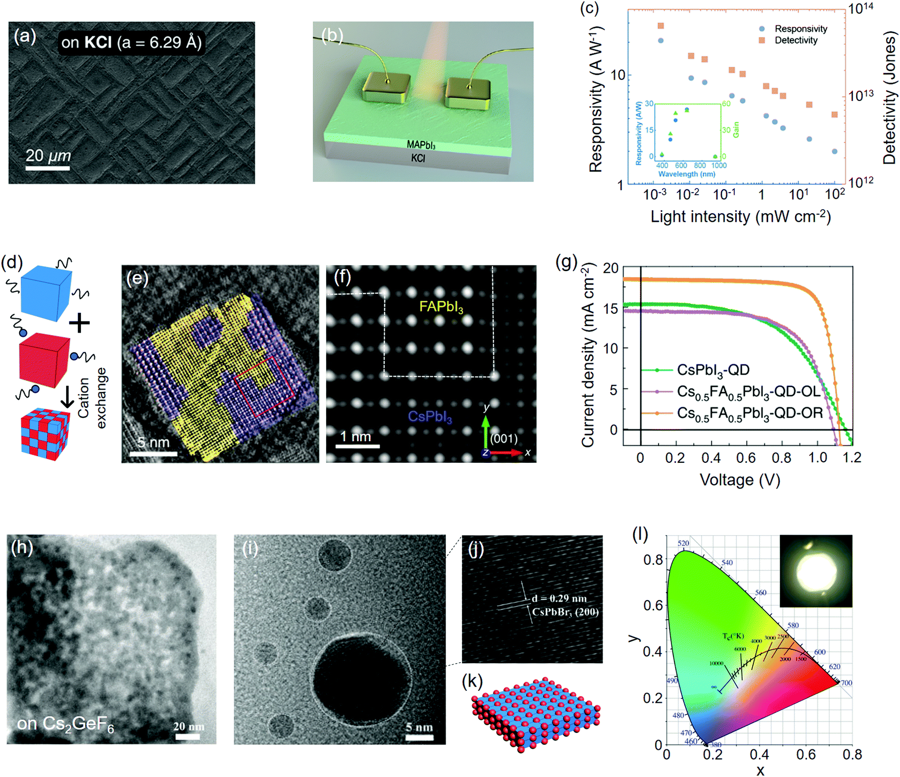 | ||
| Fig. 6 Perovskites epitaxially grown on metal halides and themselves. (a) Scanning electron microscopy (SEM) images of MAPbI3 films deposited on the KCl(001) substrate. (b) Device configuration of the corresponding MAPbI3 photodetector. (c) Plots of responsivity and detectivity of the photodetector as a function of incident light intensity. (a–c) Reproduced with permission: Copyright 2018, American Chemical Society.57 (d) Schematic illustration of cation exchange facilitated by the ligand carrier. (e) The HADDF-STEM image of the FA0.5Cs0.5PbI3 quantum dot (QD). FAPbI3 and CsPbI3 lattice are colored by yellow and purple, respectively. (f) Simulated HADDF-STEM image of the red square in (e) after reconstruction. (g) Photocurrent–voltage (J–V) curves of QD solar cells. (d–g) Reproduced with permission: Copyright 2020, Nature Publishing Group.101 (h) Transmission electron microscopy (TEM) image of CsPbBr3 QDs on the Cs2GeF6 host. (i) Enlarged TEM image of CsPbBr3 QDs. (j) Lattice spacing of the CsPbBr3 QDs. (k) Structural motif of the Cs2GeF6/CsPbBr3 heterostructure. (l) CIE color coordinates of Cs2GeF6:Mn4+/CsPbBr3 white-emission LED (WLED) under operation. (h–j and l) Reproduced with permission: Copyright 2019, Wiley-VCH.79 | ||
Spinodal decomposition as an unordinary strategy to form perovskite heterostructures, whereby one thermodynamic phase decomposes into two phases, can be regarded as a complementary strategy to build halide-varied heterostructures. For instance, lateral double-heterostructure MAPbIxBr3−x NWs were prepared with the classic coarsening kinetics regulated by photon illumination.198 The periodical distribution of halide segregation induced I-rich and Br-rich phases within one single NW showed reduced Fröhlich electron–phonon coupling in comparison to the homogeneous one. As oppose to the halide reconstruction-induced heterostructure formation, Cao et al.228 recently found that the MAPbI3/MAPbCl3 component would not alloy but rather result in a natural phase-segregated status. The quasi-epitaxial interface between MAPbI3 and MAPbCl3 achieved ultrafast charge carrier transfer time of about tens of picoseconds.
A-site cation exchange enables the formation of perovskite heterostructures that can hardly be discerned by their crystal color. Although a few literatures have demonstrated that segregated ABX3 phases can coexist in the multi-cation perovskite,229,230 there is no convincing evidence to prove that these phases can be bound to each other with an atomically sharp interface. Most recently, Hao et al.101 synthesized FA1−xCsxPbI3 QDs by mixing CsPbI3 and FAPbI3 QDs in a colloidal solution with the existence of OL ligands. Cation exchange among these QDs was facilitated by OL, thus leading to the rapid formation of cation-mixed QDs (Fig. 6d). The authors employed high-angle annular dark field scanning transmission electron microscopy (HAADF-STEM) to clearly observe the lattice coherence between CsPbI3 and FAPbI3 within one crystal (Fig. 6(e and f)). Solar cells based on these FA0.5Cs0.5PbI3 QDs yielded a certified PCE of 16.6% with benign photostability (Fig. 6g and Table 1).
B-site cation substitution provides another solution to epitaxially bind perovskite in the double perovskite lattice. Wei et al.79 reported the in situ growth of CsPbBr3 QDs on the host edge of the Cs2GeF6 double perovskite via chemical converting the sequentially grown PbBr64− multilayers whose Cs+ source is afforded by the host. The incommensurate lattice accommodation of CsPbBr33(100)‖Cs2GeF62(100) (f ≈ 2.7%) guarantees the feasibility of epitaxy in principle. Also, the well dispersed CsPbBr3 QDs on the Cs2GeF6 host mitigated the optical degradation under continuous illumination. Doped with Mn4+, a bright white light emission was achieved on the LED device based on Cs2GeF6:Mn4+/CsPbBr3 heterocrystals, with a Commission International de L’Eclairage (CIE) color coordinate of (0.32, 0.33) (Table 3). In addition, the authors of this study observed strong green luminescence when the Cs2GeF6 host was replaced with Cs2SiF6, Cs2TiF6, and Cs2ZrF6.
Supported by interlayer organic spacers, low-dimensional (LD) perovskites can form an epitaxial relationship among different perovskite QWs (defined by the layer number of n) through vdW interaction.190 This statement was experimentally examined by some recent studies on both Ruddlesden–Popper (RP) (PEA)2MAn−1PbnI3n+1 and Dion–Jacbson (DJ) (HA)(FA)n−1PbnI3n+1 (HA, histammonium) below the n value of 5.192,231 The authors all observed clear vertical-stacked layers on the as-grown single crystals. In terms of energy conversion applications, one of the most significant advantages of the 2D/3D QW-heterostructures is the energy funnels created among the bandgap-varied QWs for efficient charge transfer. Yuan et al.73 previously employed transient absorption (TA) technique to prove that the (PEA)2MA4Pb5I16 prepared at the film state was composed of multiple wide-bandgap 2D and low-bandgap 3D phases. The energy landscape within these heterostructures well suppressed the non-radiative recombination and gave rise to a maximum external quantum efficiency (EQE) of 8.8% and a stabilized radiance of 80 W sr−1 m−2 for LED under the driven voltage of 7.4 V. Zhao et al.75 later evidenced the coexistence of 2D and 3D phases in NMAI (NMA, 1-naphthylmethylamine)- and polymer-mixed FAPbI3 by their lattice spacings. Their LED device delivered an EQE up to 20.1% under the current densities of 0.1–1 mA cm−2 (Table 3).
2D QWs are also believed to stabilize the 3D perovskite phases and hence offer a compromise between the performance and stability of PSCs. By introducing BA+ spacers into the FA0.83Cs0.17Pb(IyBr1−y)3 absorber, Wang et al.104 found that plate-like crystals that emerge beside the regular shape ones were increased relative to the increasing volume of BAI. The 2D/3D QW-based PSCs yielded reduced hysteresis along with stabilized power output; moreover, the optimal PCE of the low-bandgap component (BA0.05(FA0.83Cs0.17)0.95Pb(I0.8Br0.2)3) reached 20.6% at that time (Table 1). Using grazing-incidence wide-angle X-ray scattering (GIWAXS) technique with different incident angles, Wang et al.107 successfully determined the vertical distribution of QWs in the PEA0.15FA0.85SnI3 film, that is, the 2D QWs lie close to surface while the 3D ones lie close to the substrate (Fig. 7(a–c)). This finding might be explained by the crystallization of LD perovskites, which is initiated from the liquid-air interface.232 A maximum PCE of up to 9.4% was finally achieved on such a hierarchical absorber (Fig. 7d and Table 1). Interestingly, an opposite vertical distribution of the 2D/3D QWs to the former case was reported on (F1PEA)2MA3Pb4I13 (F1PEA, fluorophenethylammonium) films, of which the pF1PEA (4-fluorophenethylammonium) entity delivered the highest PCE of 11.4% for PSCs (Table 1).108
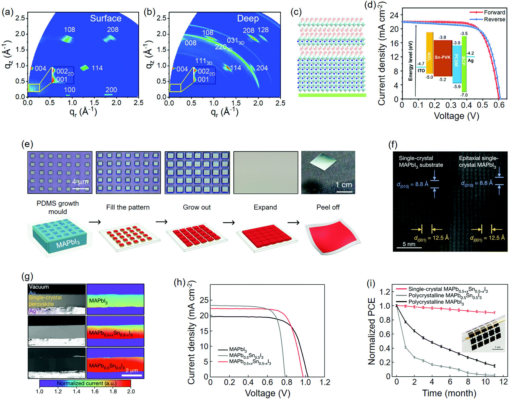 | ||
| Fig. 7 Perovskites epitaxially grown on 2D QWs and themselves. (a) GIWAXS pattern of the PEA0.15FA0.85SnI3 film with an incident angle of 0.2°. (b) GIWAXS pattern of the PEA0.15FA0.85SnI3 film with an incident angle of 2°. (c) Schematic of hierarchical 2D/3D QWs perpendicular to the substrate. (d) J–V curves of the corresponding PSC. (a–d) Reproduced with permission: Copyright 2018, Elsevier Inc.107 (e) Optical images (top) and preparation schematics (down) of liquid-phase epitaxy of single crystalline perovskite thin film and its transfer process. (f) TEM images of the interfacial lattice of homoepitaxial MAPbI3. (g) Cross-sectional SEM images and corresponding electron-beam-induced current (EBIC) mapping of three different single crystalline perovskite components. (h) J–V curves of PSCs based on three components. (i) Long-term shelf-stability test of flexible PSCs upon the transferred single crystalline perovskite absorbers. The inset is the optical image of the device. (e–i) Reproduced with permission: Copyright 2020, Nature Publishing Group.102 | ||
In contrast to the heterostructures built on different perovskite components, the homoepitaxy of perovskites on themselves creates a consistent interfacial lattice without mismatch or strain. A supersaturated precursor solution can avoid the dissolution of the perovskite substrate during liquid-phase homoepitaxy. This strategy has been widely employed to grow large-sized perovskite single crystals at a slow rate.183–185 Under similar circumstance, Lei et al.72 studied the solution-homoepitaxy of MAPbBr3 on the patterned MAPbBr3 single crystal substrate whose parylene-C coating layer was pre-treated by lithography. By controlling the growth temperature, growth time, and pattern geometry, the diversified structure and orientation of MAPbBr3 single crystal arrays were achieved. The authors deduced a layer-by-layer growth mode from the clear edge between each individual MAPbBr3 layer, which is magnified by the terrace morphology of {001} facets. Importantly, the epitaxial crystal arrays exhibited a carrier lifetime (including fast and slow components), which is far longer than its polycrystalline counterpart, and the lifetime dropped if the growth rate was accelerated (corresponding to higher growth temperature). These individual single crystals showed strong and uniform green light emission as LED arrays with a maximum EQE of 6.61% (Table 3). Besides, negligible EL peak shifting was observed under increasing drive voltage from 2 V to 10 V. In their most recent work, MAPbI3 was epitaxially grown on the MAPbI3 single crystal substrate moulded by lithography-treated polydimethylsiloxane (PDMS) (Fig. 7(e and f)).102 The perovskite arrays merged into a thin film and was then transferred into a flexible substrate by a parylene layer. The authors found that the single crystal graded perovskite absorber (MAPb0.5+xSn0.5−xI3) could deliver champion PV performance compared to the MAPbI3 and MAPb0.5Sn0.5I3 counterparts (Fig. 7(g and h)). A small PCE decline was observed for the MAPb0.5+xSn0.5−xI3 flexible solar cells during the 11-month stability test, which was contrasted by the almost full degradation of the polycrystalline ones (Fig. 7i).
3.3 V/VI-based materials
Nitrides, oxides, and chalcogenides are representative of three important classes of V/VI-based compounds. Being integrated with perovskites, their semiconductor counterparts have given rise to many state-of-the-art optoelectronic devices, either in the form of stacked multilayer or well-defined delicate heterostructures. In this section, we focus on a few prime examples of perovskites epitaxially grown with these materials, encompassing nitrides, metal oxides, quartz, and metal monochalcogenides.Perovskite oxides (ABO3), as structural analogs to halide ones, can be regarded as good substrates to commence high-quality epitaxy. Chen et al.60 previously reported continuous CsPbBr3 single crystalline film grown on SrTiO3(100) at the CVD temperature of 450 °C (Fig. 8a) and the thickness of the perovskite film can be readily adjusted by varying the vapor deposition time. The incommensurate lattice accommodation was demonstrated to be CsPbBr32(100)‖SrTiO33(100) with a low f value of 0.47%. Also, the photodetectors based on the CsPbBr3 single crystalline film showed fast photoresponse time of a few milliseconds under the simulated 1 sun illumination (Fig. 8(b, c) and Table 2). The authors also found that when the substrate was altered to SrTiO3(110), a few prisms appeared on the CsPbBr3 crystals, which were supposed to be the exposed (110) facets of CsPbBr3. Kelso et al.233 recently studied the in-plane rotated (45°) accommodation of spin-coated CsPbBr3 thin-film crystals on SrTiO3(100). Determined from the coincidence sites, such coherence mode reduces the f value from −49.3% (regular one-on-one) to −5.57% (in-plane rotated one-on-two).
 | ||
| Fig. 8 Perovskites epitaxially grown on metal oxides. (a) SEM image of the CsPbBr3 single crystalline film on SrTiO3(100). (b) Current–voltage (I–V) curves of the CsPbBr3 photodetector. (c) Photoresponse of the device under a bias voltage of 2.5 V. (a–c) Reproduced with permission: Copyright 2017, American Chemical Society.60 (d) CsPbBr3 NWs grown on the annealed M-plane sapphire. (e) Cross-sectional TEM image of the M-plane sapphire/CsPbBr3. (f) Rise and fall times of the CsPbBr3 photodetector (device configuration: Au/CsPbBr3/Au). (d–f) Reproduced with permission: Copyright 2017, American Chemical Society.62 | ||
Sapphire, which is mainly composed of aluminium oxide (α-Al2O3), has been widely used as an epitaxial substrate for conventional LED chips. Via the CVD method, Shoaib et al.62 prepared ultralong CsPbBr3 NWs with consistent in-plane orientation along the [1−210] direction on the annealed M-plane sapphire (Fig. 8d). The graphoepitaxy was revealed by the cross-sectional TEM characterization, as the triangular CsPbBr3 NW fully filled the V-shaped nanogrooves of the M-plane sapphire (Fig. 8e). The as-grown high-quality single crystals exhibited an ultrahigh responsivity of 4400 A W−1 with short rise/fall times of 252/300 μs (Fig. 8f and Table 2). Moreover, the authors found that the large-sized microcrystals on the M-plane sapphire showed same orientational features under lower deposition pressure. Oksenberg et al.234 meanwhile studied the response speed of the photodetectors based on CsPbBr3 NWs grown on the C-plane and the annealed M-plane sapphire. The horizontal aligned CsPbBr3 NWs on the annealed M-plane sapphire exhibited ultrafast rise/fall times of 10/5 μs, in contrast to the 71/68 μs of 6-fold symmetrical NWs on the C-plane sapphire. Interestingly, Wang et al.235 later demonstrated a large Rabi splitting energy of CsPbX3 NW arrays grown on the annealed M-plane sapphire. The lasing action of NWs was mainly focused on two sides when pumping was above the lasing threshold. Most recently, CsPbBr3 single crystals were reported to be epitaxially grown on the cubic zinc oxide (ZnO) single crystal substrate with a significantly improved PL stability, although the f value of CsPbBr3(100)‖ZnO(100) was declared to be as high as 19%.236
Particularly notable is that cutting quartz (mainly composed of SiO2) along certain directions will create a periodic topology for orientational control of the perovskite epilayers. Earlier, Li et al.237 studied the growth characteristics of slip-coating MAPbI3 on multi-axis cut quartz. They found that only ST-cut quartz substrate (intervals along [100] direction) supported the orientational growth of MAPbI3 toward the microribbon arrays (length up to sub-millimetre scale), whereas the others (X-, Y-, Z-cut quartz) would lead to a randomly oriented morphology. The well-aligned growth of the perovskite on ST-cut quartz was demonstrated to occur regardless of the slipping directions and the f value of MAPbI33(001)‖quartz2(100) was determined to be 3.2%. More recently, the authors synthesized ultralong MAPbI3 NWs on ST-cut quartz, which were sandwiched by the Si wafer cover.61 The length of the NWs can be facilely tuned by varying the concentration of the perovskite precursor solution. The 1D perovskite structure in the above two cases both showed preliminary capability for photodetector applications (Table 2).
 | ||
| Fig. 9 Perovskites epitaxially grown on metal monochalcogenides. (a) SEM images of the PbSe@CsPbBr3 wire at different growth times. (b) Time-dependent photoresponse of the PbSe@CsPbBr3 photodetectors. (a and b) Reproduced with permission: Copyright 2018, Wiley-VCH.64 (c) TEM image of the CsPbI2Br lattice anchored on PbS CQD under high volume ratio of CQDs. (d) TEM image of PbS CQD in the CsPbI2Br matrix under low volume ratio of CQDs. (e) J–V curves of pure PbS CQDs and PbS/CsPbI2Br solar cells. (c–e) Reproduced with permission: Copyright 2019, Nature Publishing Group.114 | ||
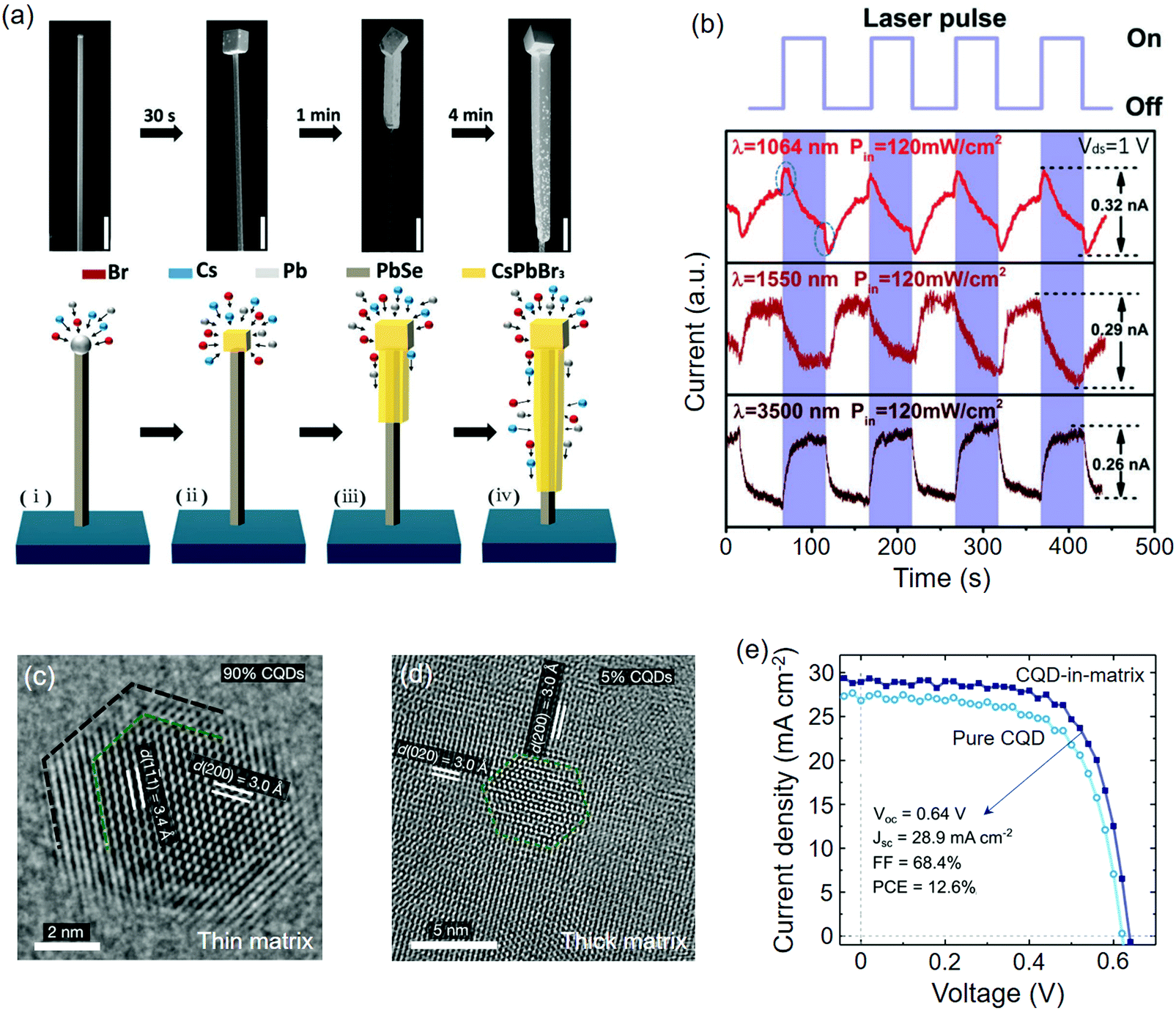
Epitaxial growth between the metal monochalcogenide and perovskites could occur in the colloidal phase if their lattice parameters are closely matched. On the basis of surface ligand exchange, Ning et al.238 added PbS CQDs into the precursor solution of MAPbI3, in which the halide ligands (MAI) exchanged the original aliphatic ones on the PbS surface; hence, an atomic-level lattice coherence between MAPbI3 and PbS could be achieved. The epitaxial relationship was determined to be MAPbI3(110)‖PbS(100) with a f value of −4.6%. Passivated by the as-grown MAPbI3, the carrier diffusion length of the hybrids was significantly extended together with a diversified spectrum. The same strategy was later performed on PbS and SnS CQDs to generate core–shell or dot-in-matrix heterostructures for solar cells with enhanced PCEs and stability.109–111 Note that these CQDs can also function as nucleation sites for large-crystal MAPbI3 absorber films.111,239 More recently, FA+ was demonstrated to be viable for exchanging the OL ligands on the PbS CQDs surface.112 The FAPbI3 film doped with PbS CQDs exhibited significantly improved ambient stability and an optimized PCE of 18% for PSC. Supported by theoretical calculations, the authors estimated that the FAPbI3 lattice is compressively strained on PbS(100), of which the strong interfacial chemical bond should be responsible for the stabilized black phase. Specifically, Liu et al.114 prepared PbS/PbSe CQDs whose surface ligands were pre-removed, hence facilitating the anchoring of all-inorganic perovskite in an epitaxial form. A nearly perfect matched lattice of CsPbI2Br(100)‖PbS(100) was revealed by their lattice spacings and the f value was identified below 0.2% (Fig. 9(c and d)). The dot-in-matrix structure (PbS CQDs in 15 vol% CsPbI2Br) showed a stabilized PCE of 12.6% for the solar cells, which was better than that of the pure CQDs (Fig. 9e).
By providing the chalcogenide precursor, colloidal synthesis via hot-injection also enables the formation of nanoscale heterostructures with an epitaxially bound lattice between the perovskite and metal monochalcogenide. For example, Zhang et al.81 sequentially injected Se-tributylphosphine and Cs-oleate into the PbX2 stock solution to synthesize CsPbBrI2–PbSe heterocrystals featuring bright red emission PLQY up to 83.4%. A lattice-match status can be created between CsPbBrI2 (a = 6.059 Å) and PbSe (a = 6.124 Å), whose f value was calculated to be 1.07%. Under the driving voltage of 4 V, the CsPbBrI2–PbSe LED device exhibited bright red emission with a CIE color coordinate of (0.70, 0.29) (Table 3).
3.4 vdW materials
The epitaxial growth of perovskites on non-layered materials usually involves strong chemical bonds at the interface. Such a growth mode is restricted by the lattice symmetry and lattice constants of both the solids. As an alternative, vdW substrates such as layered oxides, transition metal dichalcogenides (TMDs), graphene, hexagonal boron nitride (h-BN), and black phosphorene (BP) support perovskite block formation through weak vdW forces, which circumvents the lattice matching requirement of conventional substrate materials. Besides, the physically assembled vdW interface allows the as-grown perovskite to be exfoliated for more flexible integrations. | ||
| Fig. 10 Perovskites epitaxially grown on vdW materials. (a) Schematic illustration of the 6-fold growth mode of CsPbBr3 NW on mica. Below is the SEM image of the as-grown CsPbBr3 NWs. (b) Optical images of CsPbBr3 NWs grown on phlogopite mica. The insets are their corresponding fast Fourier transform (FFT) patterns. (c) Current–time (I–t) curves of the corresponding CsPbBr3 photodetector. (a–c) Reproduced with permission: Copyright 2017, American Chemical Society.241 (d) TEM image of MoS2/MAPbI3. On the right are the lattice spacings of MoS2(110) and MAPbI3(004). (e) Selected area electron diffraction (SAED) patterns of MoS2/MAPbI3. (f) J–V curves of PSCs with/without the MoS2 interlayer. (d–f) Reproduced with permission: Copyright 2019, Wiley-VCH.115 (g) TEM image of h-BN/CsPbBr3. (h) Lattice spacings of h-BN (BN) and CsPbBr3 (CPB). (i) PL stability of h-BN/CsPbBr3 in ambient air. The inset is the EL spectra of monochrome LEDs and combined WLED based on UV InGaN chip (purple region), h-BN/CsPbCl1.8Br1.2 (blue region), h-BN/CsPbBr3 (green region), and h-BN/CsPbBr1.2I1.8 (red region). (g–i) Reproduced with permission: Copyright 2019, Royal Society of Chemistry.193 | ||
In contrast to multi-fold growth, Gao et al.243 used the CVD method to prepare ultrathin CsPbX3 (X = Br, Cl) NWs well-aligned to the muscovite mica substrate in the [100] direction. Due to electrostatic dielectric confinement, the CsPbBr3 NWs exhibited strong thickness-dependent emission anisotropy and the spectra of thick NW was similar to that of the square piece, which has a negligible anisotropic feature. More interestingly, under the effect of desynchronized deposition and exchange reaction of the halide ions, the composition-graded CsPbBrxI3−x NWs were obtained on muscovite mica through vapor-phase epitaxy.244 A position-dependent dual color laser (wavelength separation: 35 nm) was produced with Br enriched at two sides and I enriched at the center. Mo et al.68 further studied the influence of vapor deposition temperature on CsPbBr3 crystal shapes. The as-grown perovskite crystals on muscovite mica showed a shape evolution from microwires (∼380 °C), microplates (∼340 °C), to triangular pyramids (∼300 °C).
Beyond the perovskite NWs, other crystal structures such as pyramids and 2D nanoplatelets are also accessible on mica. Mi et al.93 first reported the MAPbBr3 pyramids grown on muscovite mica under a CVD temperature of 345 °C; this was even earlier than the non-epitaxial cases of CsPbBr3 pyramids grown on Si wafer.89,90 The authors found that by coating the mica substrate beneath with a thin layer of Ag, the lasing threshold of the F–P pyramid cavity was reduced from ∼92 to ∼26 μJ cm−2, which is presumably due to reflected emission from the bottom facet of the pyramid by the Ag film. As the processing temperature rose to 550 °C, Zhang et al.245 synthesized high-quality CsPbX3 rectangular nanoplatelets on muscovite mica. A declining emission was observed for CsPbBr3 WGM microcavities from the corner and edge to the center area. By varying the halide composition, a multi-color (410–700 nm) excitonic laser was achieved with a low threshold of ∼2.0 μJ cm−2 (400 nm excitation) and high spectral coherence (0.14–0.15 nm). In addition, the space-confined CVD method was introduced to obtain square-like CsPbI3 nanosheets with the thickness down to 6 nm.95 The growth spacing between the two stacked mica pieces can be artificially adjusted to meet the thickness needed and the as-prepared CsPbI3 nanosheets showed one/two-photon infrared-pumped lasing with a threshold of 2.6 mJ cm−2 under 1200 nm excitation.
The vdW gap creates a natural space to isolate an epilayer from the vdW substrate; however, it is thought that such a space is not far enough to entirely screen the impact from the matter below the substrate surface.248,249 The concept of remote epitaxy is introduced by inserting the monolayer vdW materials to the interface. For example, Jiang et al.160 inserted monolayer graphene as a buffer in the heterostructures constructed by polar substrates (NaCl and CaF2) and the vapor-deposited CsPbBr3 epilayer. Upon simulation results, monolayer graphene lowered the interfacial interaction energy between CsPbBr3(001) and NaCl(001), indicating its good screen effect on the electrostatic potential. This unique growth mode enabled controllable dislocation density on CsPbBr3, which significantly enhanced the PL intensity of the perovskite film. In addition, pyrolytic graphite, which consists of multilayer graphene, was recently reported to fabricate transferable CsPbBr3 microplatelets for EL and lasing applications.250
Alternating N and B atoms in hexagonal rings builds a single layer of h-BN without the surface dangling bonds. Via the hot-injection method, CsPbX3 NCs were in situ grown on exfoliated h-BN nanosheets to form the vdW heterostructure (Fig. 10(g and h)).193 Their WLED devices upon the combined emitters of UV chip, h-BN/CsPbCl1.8Br1.2, h-BN/CsPbBr3, and h-BN/CsPbBr1.2I1.8 displayed a wide color gamut with a CIE color coordinate of (0.372, 0.322) (Fig. 10i). Moreover, the assembled h-BN greatly improved the thermal and moisture tolerance of the perovskite. By directly mixing the perovskite precursors with h-BN in the OA/OL-stabilized colloidal solution, Li et al.82 synthesized h-BN/CsPbBr3 nanocomposites with a recoverable PL behavior during the thermal stability test. The WLED device stacked by blue chip, red phosphors, and nanocomposites showed a color-rendering index (CRI) of 76 and a luminous efficiency of 57 lm W−1 (Table 3).
BP, as another layered monoelemental material, can also commence the vdW growth of perovskites. By controlling the spin-coating times of the aqueous dispersion of monolayer BP, Zhang et al.116 prepared the vdW-grown triple-cation perovskite film on thickness-tailored BP substrate. The dual interlayers of BP on both the top and bottom sides of the perovskite film were demonstrated to create an energy cascade for PSCs, hence enhancing their PCEs from 16.95% (BP-free) to 19.83% (Table 1). Multilayer-stacked BP is called black phosphorus (BPs). Chen et al.71 synthesized the BPs/CsPbBr3 heterostructure in a colloidal solution. Compared to the hybrid one that was only spaced by surfactant ligands, the in situ grown CsPbBr3 NCs on BPs showed an enhanced charge transfer efficiency between each other and the as-assembled photodetector exhibited a detectivity of up to 2.6 × 10¹¹ Jones (Table 2). More recently, BPs QDs were introduced into the CsPbI2Br precursor solutions in order to serve as the heterogeneous nucleation sites for large grain size perovskite films.117 The embedded BPs QDs in the perovskite crystals led to excellent internal charge extraction, accompanied by the reinforced film stability in ambient air. The highest PCE of the assembled PSC was enhanced to 15.47% with the addition of 0.7 wt% BPs QDs, compared to 9.26% for the pristine one (Table 1).
3.5 Conversion from epitaxial lead compounds
The convertible property of lead halides has made their design into intermediates toward perovskites possible from both liquid- and vapor-phase processing. The intercalation reaction of epitaxial lead halides as a special growth mode toward perovskite epitaxial structures can support the conformal growth of perovskites in vapor-phase deposition. Earlier, Ha et al.251 reported 2D MAPbI3 microplatelets, which were intercalated from the epitaxial PbI2 microplatelets on muscovite mica by the CVD method. The gas–solid reaction allowed high duplication on the lateral crystal profiles and only altered their final thickness. This conversion strategy is exceptionally suitable for preparing patterned perovskite solids on monolayer vdW substrates that can be treated by lithography (e.g., MoS2, h-BN, and graphene).213,252 With precisely controlled CVD temperature, a few nanometer-thick PbI2 layer was successfully prepared on the WS2 monolayer substrate, whereby ultrathin MAn+1PbI3n+1 layers (as thin as 2.7 nm) can be finally obtained in vapor-phase conversion.35 A distinct layered feature of the as-grown MAn+1PbI3n+1 was revealed by the authors through the cross-sectional TEM image. It is noteworthy that the photoresponsivity (11174.2 A W−1 under 520 nm illumination) and response time (64 μs) of the photodetectors based on ultrathin perovskite solids (5.2 nm) were both measured to be 4 orders of magnitude superior than that of the thick one (36.2 nm) (Table 2). Recently, the seamless graphene monolayer was demonstrated to serve as a vdW substrate for the epitaxial PbI2 film.70 The as-converted MAPbI3 film showed the advantageous application of flexible photodetectors, whose responsivity reached an ultrahigh magnitude of 107 A W−1 under 633 nm illumination (Table 2).Taking advantage of the electrochemical synthesis, the lead compounds were allowed to be epitaxially grown on the well-orientated Au single crystal substrates. For example, the in-plane order of the electrodeposited PbI2 films was demonstrated to nearly follow the orientation of the Au [(100)/(110)/(111)] substrates.222 Also, the fiber textured MAPbI3 films featuring the [110] out-of-plane orientation was later obtained via vapor-phase conversion though it has no relevance to the preferred orientation of the PbI2(0001) templates. In the case of MAPbI3 films converted from the electrodeposited PbO2 layers on Au[(100)/(111)], the lattice accommodations of MAPbI3(001)‖PbO2(100) and MAPbI3(110)‖PbO2(100) were found to be retained regardless of the orientation of the Au substrates and the f values were measured to be −1.2% and 2.2%, respectively.155 Importantly, either the textured (from PbO2 on Au-coated glass) or epitaxial [from PbO2 on Au(100)] MAPbI3 films possessed lower trap densities compared to the polycrystalline film (spin-coated PbI2 on Au-coated glass). The conversion pathway of PbO2 can be expressed by the following chemical equation to discriminate it from the intercalation reaction of PbI2.
| PbO2 + 5MAI → MAPbI3 + I2 + 4CH3NH2 + 2H2O |
4. Mechanical and physical interrelation at the interface
The epitaxial growth of perovskites with various materials have produced a myriad of combinations owning novel properties and functionalities. Given the potential heavy impact from substrates, it is of basic importance to make out their mechanical and physical interrelations with the perovskite adlayers. In this section, from the perspectives of strain and electronic structure, we move beyond the as-discussed epitaxial structures in Section 3 and examine these interactions between two distinct solids either integrated in the epitaxial or the non-epitaxial form. These two parts are able to rationalize many unusual behaviors of the junctions, such as variable photophysical properties, anomalous operation stability, and exceptional charge carrier dynamics.4.1 Interfacial lattice strain
At the interface with varied lattice parameters, the epilayers are typically strained to accommodate the substrates. As a result, local lattice distortion emerges at the interface to relax the strain and eventually evolves into structural defects such as dislocations.151,152 Another aspect is that perovskites, especially organic–inorganic hybrid ones, possess a considerably large thermal expansion coefficient,253,254 which can be embodied in the distinct lattice expansion/contraction phenomena during thermal annealing/cooling255,256 or under light illumination.257 The strain-based perovskite adlayers give added flexibility to the property and functionality design of the heterostructures. In this view, we have summarized the lattice accommodations that can originally cause strain within the epitaxial structures; some non-epitaxially strained cases induced by other reasons are also provided (Fig. 11).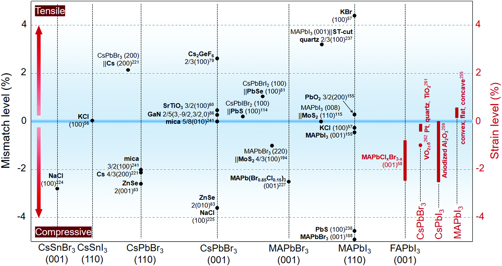 | ||
| Fig. 11 Lattice mismatch level between epitaxial perovskites and substrate materials (black characters). The right axis is the strain level of the perovskites determined in the in-plane direction (red characters). | ||
The angle shift of the diffraction peak is an important index to judge the lattice spacing variation of the crystals, which can be further referred to as a determinant of the lattice strain. Substrate-induced residual strain within a regular perovskite film was not exactly affirmed until a recent study about the MAPbI3 films deposited on glass and quartz.258 The amorphous glass substrate was demonstrated to impose in-plane compressive strain on the perovskite film and suppress the crystal growth. By contrast, a promoted phase transition from tetragonal to orthorhombic was observed on the strain-relaxed quartz substrate and thus led to modified PL response at room temperature. Zhao et al.255 conducted in-depth research on the strain influence from the substrate shape. When being deposited on a flat substrate, the thermal-induced out-of-plane compression and in-plane tensile strain on the MAPbI3 polycrystalline films was identified to lower the activation energy of ion migration, thus accelerating the perovskite phase decomposition. By contrast, a concave-shaped substrate with a similar thermal expansion coefficient to that of MAPbI3 relaxed the strain efficaciously. The resulting perovskite film showed an enhanced light stability with enhanced activation energy for ion migration.
Inside the nanoporous anodized aluminium oxide (AAO) framework, the pore wall-induced 3D compressive strain on the CsPbI3 crystals was judged by the lattice spacings.259 The detailed strain level was calculated following a modified Williamson–Hall rule, which is expressed by:260
| Δdobs2 − Δdins2 = Δdsize2 + ε2d2 |
Besides the geometric impact, the strain behavior of the perovskite adlayers relative to the substrate materials have been systematically studied upon a few combinations. For example, using scanning X-ray diffraction microscopy (SXDM), Li et al.261 successfully measured the substrate-induced lateral strain variations within one single perovskite crystal. A thermal expansion mismatched platform was created on the Pt-patterned quartz substrate, leading to gradient in-plane compressive strain levels on the as-grown CsPbBr3 crystal near the quartz-Pt transition region. Such nanoscale strain distribution was embodied in the PL mapping, as the PL peak showed a blue-shift due to strain relaxation on the Pt substrate. The authors of this study further found that the common TiO2 substrate would impose stronger compressive strain on the CsPbBr3 crystal compared to the quartz and Pt substrates. Specifically, a dynamic strain engineering concept was raised by Wang et al.262 regarding the metal–insulator transition behavior of VO2±δ among oxygen-deficient V2O3, VO2, and oxygen-sufficient V2O5. The phase transition among original (M1), monoclinic (M2), triclinic (T), and metallic rutile (R) phases, which was caused by composition, strain, and temperature variations, enabled a dynamic strain exertion on the as-coated perovskite layer. Under a sufficiently large entailed compressive strain (up to ∼1%) of the VO2 nanoforest arrays, the temperature-dependent phase transition of vapor-deposited CsPbBr3 (from α to β) was triggered, which is embodied in the peak splitting of the PL spectra. The authors further held that dense arrays of VO2±δ NWs are supposed to produce potential bulk strain with more flexibility on the composition choices of the perovskites.
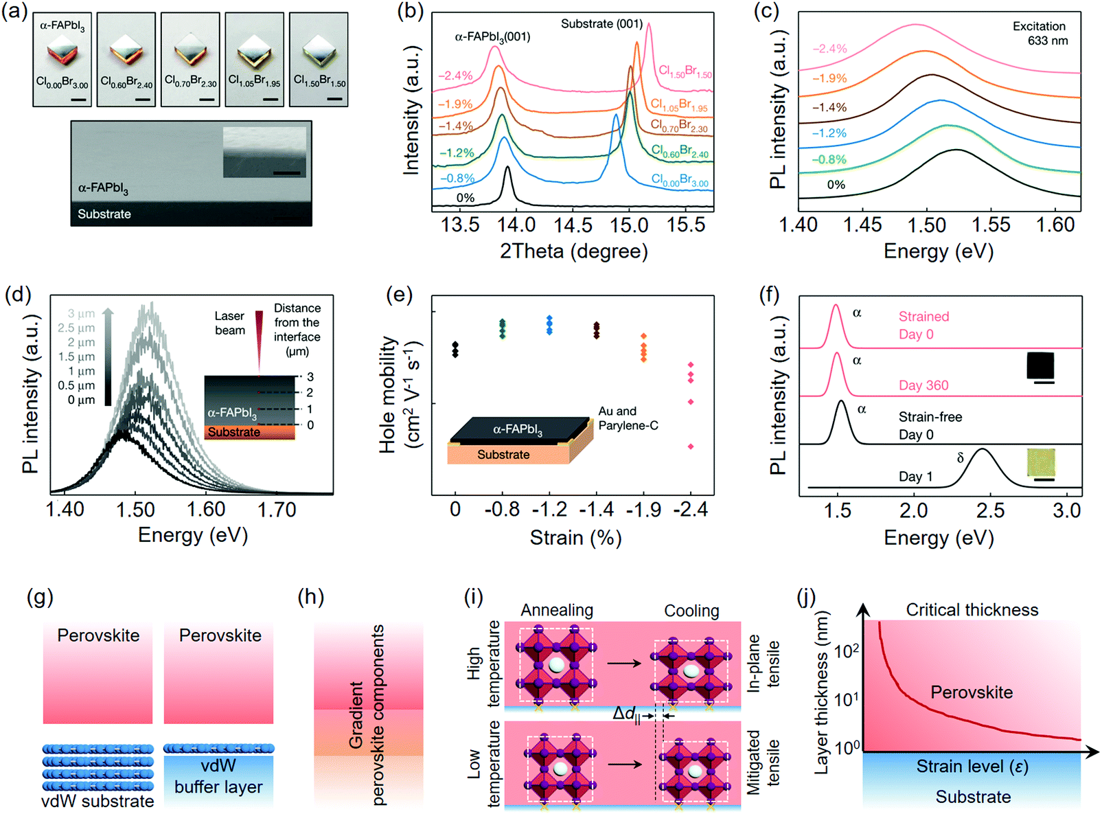
Chen et al.58 recently prepared in-plane compressively strained α-FAPbI3 films on MAPbBrxCl3−x single crystal substrates (Fig. 12a) as a contrast to the strain-free one on the α-FAPbI3 single crystal substrate. The halide variation alters the lattice constant of MAPbBrxCl3−x; therefore, it can be artificially designed to impose certain strain levels on epitaxial α-FAPbI3 films. The in-plane lattice expansion was intuitively reflected by the low-angle shift of FAPbI3(001) (Fig. 12b), indicating a compressive lattice strain on the perovskite epilayer, which is parallel to the substrate. Such a strain lifted the valence band maximum (VBM) of α-FAPbI3 and narrowed its bandgap from 1.523 eV (strain-free) to 1.488 eV (strain level: −2.4%) (Fig. 12c). To determine the vertical strain distribution of the perovskite epilayer, the authors used confocal PL technique to collect signals at different depths. The relaxed strain from the bottom to the top surface was reflected by the distinct blue-shift PL peaks (Fig. 12d), which is in agreement with the established vertical strain distribution model. By contrast, the strain-free film exhibited negligible PL shift. Hall effect measurements showed that the −1.2% level entity gave rise to the highest hole mobility among p-type epitaxial FAPbI3 films (Fig. 12e). The quality of the as-prepared single crystalline α-FAPbI3 films is comparable to those produced from vapor-phase deposition and the responsivity of the strained perovskite photodetectors could reach up to 1.3 × 10⁶ A W−1 under 685 nm illumination (Table 2). Moreover, perovskite films under −2.4% strain level showed superior phase stability during the aging test, whereas the strain-free one (film thickness of ∼10 μm) could not even survive the first day (Fig. 12f).
 | ||
| Fig. 12 Lattice mismatch-induced strain and their relaxation strategies. (a) Optical images of epitaxial α-FAPbI3 films on MAPbClxBr3−x single crystal substrates. Below is the cross-sectional SEM image of one representative entity. (b) XRD patterns of MAPbClxBr3−x/α-FAPbI3. (c) PL spectra of MAPbClxBr3−x/α-FAPbI3. (d) Confocal PL spectra of a 3 μm-thick α-FAPbI3 film. (e) Hall mobilities of α-FAPbI3 films under different strain levels. (f) Fresh and aged samples of strain-free and strained α-FAPbI3 films. (a–f) Reproduced with permission: Copyright 2020, Nature Publishing Group.58 (g) Strain relaxation by vdW epitaxy. (h) Reduced mismatch of the perovskite–perovskite heterostructure by the creation of a composition-graded interface. (i) Mitigating the in-plane tensile strain by lowering down the processing temperature. (j) Conceptual strain model of the perovskite epilayer versus its vertical thickness. | ||
Grounding on the existing strain researches, a general conclusion can be reached, that is, the in-plane tensile strain might be an undesired component for perovskites, largely because of its negative impacts on the perovskite phase stability. Borrowing from these results, meanwhile, a few advisable strategies have been designated toward future strain engineering of perovskite epilayers, especially for those targeting energy conversion applications: (i) strain relaxation would probably be an ongoing topic in order to minimize the defect formation energy at the substrate/perovskite interface. vdW materials that circumvent the lattice match with perovskites might therefore be a good choice for epitaxial substrates (Fig. 12g); (ii) the intentionally or unintentionally created composition-graded interface between two perovskites components has a potential to well connect the lattice in view of its gradient lattice parameters; hence, the strategy can be adopted to relax the strain within the perovskite–perovskite epitaxial heterostructures (Fig. 12h); (iii) lowering down the solution processing temperature of the perovskites (e.g., in vacuum condition), particularly for organic–inorganic hybrid ones that have high thermal expansion coefficients, might be practical to reduce the in-plane tensile strain of the perovskite epilayers (Fig. 12i); (iv) in-plane or 3D compressive strain has shown its ability to simultaneously optimize the photophysical properties and stability of the perovskites; more substrate materials are worth screening following the rule of lattice accommodation or being geometrically tailored; (v) the critical thickness of the perovskite epilayer is untapped so far; thus, it might point a way to eliminate the strain impact by increasing the overall layer thickness (Fig. 12j).
4.2 Energy level alignment
Electronically contacted solids with unequal bandgaps are of basic technological importance to control the mutual charge carrier transfer within heterostructures and hence to govern the optoelectronic performance of devices. The basic alignment models of semiconductor heterojunctions can elucidate a majority of perovskite-semiconductor contact (Fig. 13a), of which type-I and type-II are the most commonly seen in interfacial analysis. Charge confinement or all-transferred effect, which is provided by the straddling type-I alignment, is able to promote or retard the carrier behavior within the perovskites, whereas type-II involves the selective extraction of electrons/holes from the perovskites. | ||
| Fig. 13 Band alignment of perovskite heterojunctions and their impact factors. (a) Straddling (type-I) and staggered (type-II) band alignment of semiconductor heterojunctions. (b) Band offset of perovskites under in-plane strain. (c) Predicted band structure evolution of perovskites relative to the layer thickness and vertical BX6 octahedra number. (d) MA+ desorption and halide vacancy-induced interfacial band offset. (e) Termination-dependent interfacial band structure of the perovskites. | ||
Strain-induced lattice deformation of the perovskite adlayers has been experimentally proved to affect both the location of the electronic bands (CB and VB) and their gap.58,263 Tensile or compressive strain imposed by the substrate at the in-plane direction (σxy) would move the bands of the perovskite downward or upward compared to the strain-free one (Fig. 13b). Also, the VB location has been demonstrated to be influenced more readily than the CB one, which is similar to the strain behavior of well-studied zinc blende semiconductors.264,265 It meanwhile echoes some experimental results that strain engineering has a greater impact on the hole carrier dynamics of perovskites.58,263 The strain-band relationship is a powerful proof to rationalize some unusual photophysical responses of the perovskite adlayer that would be otherwise thought to be caused by some uncertain reasons.
Vapor-phase deposition enables the formation of the perovskite layer with highly controllable thickness; thus, it can be employed to analyze the band structure evolution of the perovskite relative to its thickness as well as the actual band status close to the substrate/perovskite interface. The substrate-dependent work function (WF) of prototypical MAPbI3 was observed by Olthof et al.,266 whose phenomena were ascribed to the natural WF of the n-/p-type substrates. Besides, the critical band bending thickness of the perovskite deposited on n-type substrates (within ∼100 nm) was found to be apparently lower than those deposited on p-type substrates. Such a result is in agreement with the previous study about the MAPbI3 layer evaporated on n-type ZnO(0001).267 Further reducing the layer thickness leads to an atomic scale counted by the number of BX6 octahedra. These vertically stacked units are capable of simultaneously moving the CB/VB downward through its number (n) increment, hence altering the alignment of the heterostructures between type-I and type-II with minor bandgap fluctuation.35 The dependence of the perovskite bands on the substrate nature and the as-grown layer thickness is depicted in Fig. 13c.
Chemical variation at the substrate/perovskite interface is another important factor that must be considered regarding the altered interfacial band alignment. A number of works have proved the catalytic property of metal oxides for the desorption of organic components in MAPbI3 (MAI, for example).266,268,269 Decomposition mainly proceeds by directing the generation of volatile substances, such as CH3NH2, NH3, and CH3I, therefore resulting in PbI2-rich stoichiometry close to the interface, which features a larger bandgap than that of the original perovskite. Such interfacial chemical loss-induced alignment change has yet to be reported for FA-/Cs-based perovskites. On the other hand, perovskites, especially iodide ones, have a low halide diffusion activation energy (as low as ∼0.1 eV for iodine vacancy,30 for example); hence, the potential point defects at the substrate/perovskite interface should be considered. Shi et al.270 theoretically studied the impact of iodine vacancy at the MoS2/MAPbI3 interface, which is created by its migration to MoS2, and then fills the sulfur vacancy. The authors predicted that the iodine vacancy will move the VB location of the perovskite downward and reverse the band offset of MoS2/MAPbI3 by interfacial dipole, which ultimately enables more efficient hole extraction from MAPbI3. Accordingly, we propose a model in Fig. 13d about the band alignment relative to the interfacial chemical variation of the perovskite.
Theoretical simulations also make it possible for researchers to gain insights into the band alignment of the heterostructures that is potentially affected by the termination. Unlike many conventional semiconductors whose interfacial atomic arrangement can be predicted by the valency balance, the termination of ionic perovskites with the substrate is more flexible. Several works have repeatedly proved that perovskites terminated with AX have higher CB/VB locations than the ones terminated with BX2 (Fig. 13e), and it seems viable for a variety of substrate materials.271–273 Haruyama et al.274 further simulated the electronic states of PbI2 terminations at different facets of tetragonal MAPbI3 by introducing vacant-type termination (absence of PbIx polyhedrons) complementary to the regular flat one. The authors declared that the vacant-type termination shows a lower energy (0.2 eV) than the flat one at the top VB location, which is supported by the results on both (110) and (001) facets.
5. Summary and outlook
The epitaxial growth of perovskites on substrate materials has realized combinations with atomically coherent interfaces for multiple phase connection that can modulate the photoelectrical properties and bring new functions into perovskite materials. Despite extensive approaches that have been developed for the epitaxy of perovskite-based materials, a comprehensive understanding of the growth kinetics as well as the exact structural and electronic state at the epitaxial interface remains to be achieved. These knowledge gaps stress the importance of meticulously identifying the surface atomic diffusion/accumulation during growth and the fine interfacial structure and electronic states, which should be useful for the rational design and optimization of the quality of perovskite epitaxial products. For example, the RHEED and grazing incidence fast atom diffraction (GIFAD) techniques that are typically used to characterize the surface structure of crystalline materials should be deeply explored to monitor the atomic kinetics of perovskite species in-situ on different substrates during epitaxy. Dangling or undercoordinated bonds that are usually rich at the interface are extremely detrimental to energy conversion devices due to the introduction of charge traps. A recent report by Ni et al.275 also presented a clear illustration of heterogeneity around the perovskite single crystal surface, implying the structural complexity of perovskite interface. Therefore, systematic depth-profiling and imaging measurements, such as coherent Bragg rod analysis and low-dose transmission electron microscopy, which can reveal the atomic structure of the perovskites, are expected to further provide in-depth information of the epitaxial interface.In addition, the epitaxial growth of wafer-scale, thin perovskite single crystalline films is still a pressing issue, especially for device applications. Recently, Lei et al.102 used perovskite single crystals as a host substrate for the growth of epitaxial centimetre-sized single crystalline perovskite films with the assistance of lithography and transfer technologies. More steps are needed for this fabrication compared with the direct growth of III–IV semiconductors on sapphire or SiC substrates. Space-confined solution growth has produced many large-area perovskite single crystal films, despite the fact that all the existing cases may not belong to epitaxy.276–278 It provides a potential route to commence wafer-scale perovskite epitaxy when combined with suitable substrates. On the other hand, the growth of thin films generally occurs in a very slow, high-vacuum crystallization condition, which cannot be readily achieved in a fast solution process. Molecular beam epitaxy (MBE) and metal–organic vapor-phase epitaxy (MOCVD), as classical vapor-phase methods for the epitaxial growth of conventional semiconductors, have yet to be developed for perovskites. Besides, some materials may serve as sacrificial substrates for the vapor-phase epitaxy of perovskite thin films, resembling the growth of graphene on Cu foil.279,280 The upscaling fabrication strategies are summarized in Fig. 14, which might boost the technological level of perovskite epitaxy for future high-throughput manufacturing. We envisage that large-area, single-crystal perovskite films with controllable thickness will be realized through the advancement of growth strategies as well as the discovery of alternative raw materials.
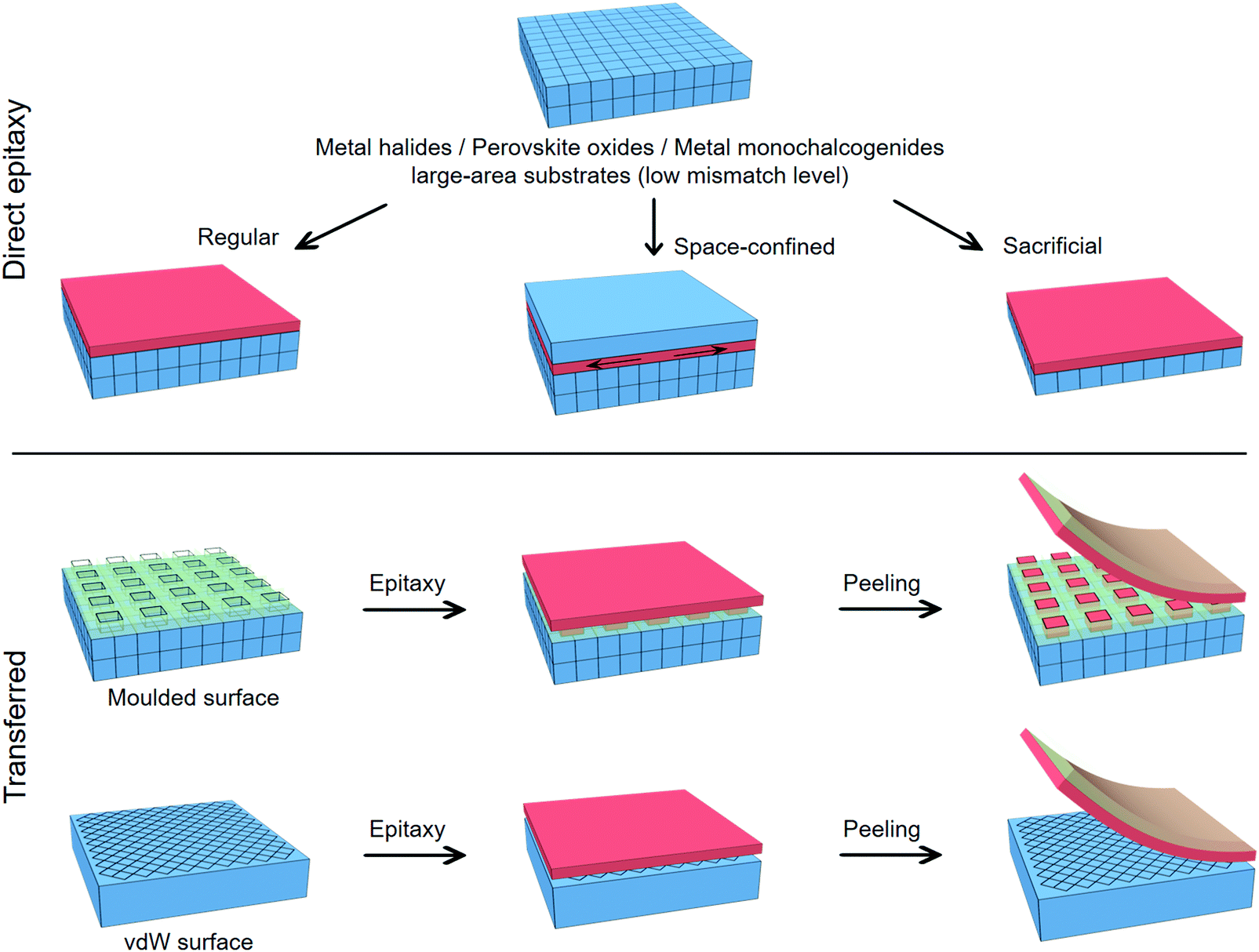 | ||
| Fig. 14 Upscaling epitaxy toward large-area and single crystalline perovskite thin films containing both direct growth and transfer methods. | ||
Although a large variety of host materials have been developed, the library of available semiconducting materials for device application is still relatively limited. Epitaxial layers in devices, such as solar cells and LEDs, require contact layers with strictly controlled thickness of about hundreds of nanometres. The most used contacting materials, such as TiO2, SnO2, and NiO, are not epitaxially compatible with perovskite materials. The epitaxial junctions using various halide perovskites would be promising to obtain high-quality devices without unbonded interface and GBs, or by using vdW materials to create bonding-free and low-defect interface. On the basis of future advances in both theory and experiment, we infer that their performance will exceed those of crystalline silicon devices in the next few years, making them competitive in the commercial market of photovoltaics and other optoelectronics.
Conflicts of interest
There are no conflicts of interest to declare.Acknowledgements
This work was financially supported by National Natural Science Fund for Distinguished Young Scholars (51725201), National Natural Science Fund for Excellent Young Scholars (52022030), National Ten Thousand Talent Program for Young Top-notch Talent, National Natural Science Foundation of China (51972111, 51902185), International (Regional) Cooperation and Exchange Projects of the National Natural Science Foundation of China (51920105003), Innovation Program of Shanghai Municipal Education Commission (E00014), the Fundamental Research Funds for the Central Universities (JKD012016025, JKD012016022), and Shanghai Engineering Research Center of Hierarchical Nanomaterials (18DZ2252400). The authors also thank the Frontiers Science Center for Materiobiology and Dynamic Chemistry.References
- H. L. Wells, Z. Anorg. Chem., 1893, 3, 195–210 CrossRef.
- D. Weber, Z. Naturforsch., B: Anorg. Chem., Org. Chem., 1978, 33b, 862–865 CAS.
- D. Weber, Z. Naturforsch., B: Anorg. Chem., Org. Chem., 1978, 33b, 1443–1445 CAS.
- A. Kojima, K. Teshima, Y. Shirai and T. Miyasaka, J. Am. Chem. Soc., 2009, 131, 6050–6051 CrossRef CAS.
- C. C. Stoumpos, C. D. Malliakas, J. A. Peters, Z. Liu, M. Sebastian, J. Im, T. C. Chasapis, A. C. Wibowo, D. Y. Chung, A. J. Freeman, B. W. Wessels and M. G. Kanatzidis, Cryst. Growth Des., 2013, 13, 2722–2727 CrossRef CAS.
- G. Xing, N. Mathews, S. S. Lim, N. Yantara, X. Liu, D. Sabba, M. Grätzel, S. Mhaisalkar and T. C. Sum, Nat. Mater., 2014, 13, 476–480 CrossRef CAS.
- B. Hu, X. Zhang, L. Liang, J. Bao, S. Li, W. Yang and Y. Xie, Adv. Funct. Mater., 2014, 24, 7373–7380 CrossRef.
- Z. K. Tan, R. S. Moghaddam, M. L. Lai, P. Docampo, R. Higler, F. Deschler, M. Price, A. Sadhanala, L. M. Pazos, D. Credgington, F. Hanusch, T. Bein, H. J. Snaith and R. H. Friend, Nat. Nanotechnol., 2014, 9, 687–692 CrossRef CAS.
- Y. Kutes, L. Ye, Y. Zhou, S. Pang, B. D. Huey and N. P. Padture, J. Phys. Chem. Lett., 2014, 5, 3335–3339 CrossRef CAS.
- M. Coll, A. Gomez, E. Marza, O. Almora, G. Belmonte, M. Quiles and J. Bisquert, J. Phys. Chem. Lett., 2015, 6, 1408–1413 CrossRef CAS.
- F. Li, C. Ma, H. Wang, W. Hu, W. Yu, A. D. Sheikh and T. Wu, Nat. Commun., 2015, 6, 8238 CrossRef.
- I. Chung, J. H. Song, J. Im, J. Androulakis, C. D. Malliakas, H. Li, A. J. Freeman, J. T. Kenney and M. G. Kanatzidis, J. Am. Chem. Soc., 2012, 134, 8579–8587 CrossRef CAS.
- C. C. Stoumpos, C. D. Malliakas and M. G. Kanatzidis, Inorg. Chem., 2013, 52, 9019–9038 CrossRef CAS.
- G. E. Eperon, G. M. Paternò, R. J. Sutton, A. Zampetti, A. A. Haghighirad, F. Caciallibc and H. J. Snaith, J. Mater. Chem. A, 2015, 3, 19688–19695 RSC.
- J. H. Noh, S. H. Im, J. H. Heo, T. N. Mandal and S. I. Seok, Nano Lett., 2013, 13, 1764–1769 CrossRef CAS.
- N. J. Jeon, J. H. Noh, W. S. Yang, Y. C. Kim, S. Ryu, J. Seo and S. I. Seok, Nature, 2015, 517, 476–480 CrossRef CAS.
- M. Saliba, T. Matsui, J. Y. Seo, K. Domanski, J. Baena, M. K. Nazeeruddin, S. M. Zakeeruddin, W. Tress, A. Abate, A. Hagfeldt and M. Grätzel, Energy Environ. Sci., 2016, 9, 1989–1997 RSC.
- M. Saliba, T. Matsui, K. Domanski, J. Seo, A. Ummadisingu, S. M. Zakeeruddin, J. Baena, W. R. Tress, A. Abate, A. Hagfeldt and M. Grätzel, Science, 2016, 354, 206–209 CrossRef CAS.
- A. D. Jodlowski, C. R. Carmona, G. Grancini, M. Salado, M. Ralaiarisoa, S. Ahmad, N. Koch, L. Camacho, G. de Miguel and M. K. Nazeeruddin, Nat. Energy, 2017, 2, 972–979 CrossRef CAS.
- J. Lin, M. Lai, L. Dou, C. S. Kley, H. Chen, F. Peng, J. Sun, D. Lu, S. A. Hawks, C. Xie, F. Cui, A. P. Alivisatos, D. T. Limmer and P. Yang, Nat. Mater., 2018, 17, 261–267 CrossRef CAS.
- C. Wang, Y. Liu, X. Feng, C. Zhou, Y. Liu, X. Yu and G. Zhao, Angew. Chem., Int. Ed., 2019, 58, 1–6 CrossRef.
- D. Liu, Q. Li and K. Wu, RSC Adv., 2019, 9, 7356–7361 RSC.
- H. Chen, Q. Wei, M. I. Saidaminov, F. Wang, A. Johnston, Y. Hou, Z. Peng, K. Xu, W. Zhou, Z. Liu, L. Qiao, X. Wang, S. Xu, J. Li, R. Long, Y. Ke, E. H. Sargent and Z. Ning, Adv. Mater., 2019, 31, 1903559 CrossRef CAS.
- H. Cho, S. Jeong, M. Park, Y. Kim, C. Wolf, C. Lee, J. H. Heo, A. Sadhanala, N. Myoung, S. Yoo, S. H. Im, R. H. Friend and T. Lee, Science, 2015, 350, 1222–1225 CrossRef CAS.
- G. Maculan, A. D. Sheikh, A. L. Abdelhady, M. I. Saidaminov, M. A. Haque, B. Murali, E. Alarousu, O. F. Mohammed, T. Wu and O. M. Bakr, J. Phys. Chem. Lett., 2015, 6, 3781–3786 CrossRef CAS.
- I. C. Smith, E. T. Hoke, D. Ibarra, M. D. McGehee and H. I. Karunadasa, Angew. Chem., Int. Ed., 2014, 126, 11414–11417 CrossRef.
- L. N. Quan, M. Yuan, R. Comin, O. Voznyy, E. M. Beauregard, S. Hoogland, A. Buin, A. R. Kirmani, K. Zhao, A. Amassian, D. H. Kim and E. H. Sargent, J. Am. Chem. Soc., 2016, 138, 2649–2655 CrossRef CAS.
- H. Tsai, W. Nie, J. C. Blancon, C. C. stoumpos, R. Asadpour, B. Harutyunyan, A. J. Neukirch, R. Verduzco, J. J. Crochet, S. Tretiak, L. Pedesseau, J. Even, M. A. Alam, G. Gupta, J. Lou, P. M. Ajayan, M. J. Bedzyk, M. G. Kanatzidis and A. D. Mohite, Nature, 2016, 536, 312–316 CrossRef CAS.
- H. Tan, F. Che, M. Wei, Y. Zhao, M. I. Saidaminov, P. Todorović, D. Broberg, G. Walters, F. Tan, T. Zhuang, B. Sun, Z. Liang, H. Yuan, E. Fron, J. Kim, Z. Yang, O. Voznyy, M. Asta and E. H. Sargent, Nat. Commun., 2018, 9, 3100 CrossRef.
- D. Meggiolaro, S. G. Motti, E. Mosconi, A. J. Barker, J. Ball, C. A. R. Perini, F. Deschler, A. Petrozza and F. D. Angelis, Energy Environ. Sci., 2018, 11, 702–713 RSC.
- J. Kang and L. Wang, J. Phys. Chem. Lett., 2017, 8, 489–493 CrossRef CAS.
- D. Shi, V. Adinolfi, R. Comin, M. Yuan, E. Alarousu, A. Buin, Y. Chen, S. Hoogland, A. Rothenberger, K. Katsiev, Y. Losovyj, X. Zhang, P. A. Dowben, O. F. Mohammed, E. H. Sargent and O. M. Bakr, Science, 2015, 347, 519–522 CrossRef CAS.
- Q. Dong, Y. Fang, Y. Shao, P. Mulligan, J. Qiu, L. Cao and J. Huang, Science, 2015, 347, 967–970 CrossRef CAS.
- M. L. Frankenheim, Ann. Phys., 1836, 113, 516–522 CrossRef.
- T. Yang, X. Wang, B. Zheng, Z. Qi, C. Ma, Y. Fu, Y. Fu, M. P. Hautzinger, Y. Jiang, Z. Li, P. Fan, F. Li, W. Zheng, Z. Luo, J. Liu, B. Yang, S. Chen, D. Li, L. Zhang, S. Jin and A. Pan, ACS Nano, 2019, 13, 7996–8003 CrossRef CAS.
- E. S. Parrott, J. B. Patel, A. A. Haghighirad, H. J. Snaith, M. B. Johnston and L. M. Herz, Nanoscale, 2019, 11, 14276–14284 RSC.
- F. Hilt, M. Q. Hovish, M. Rolston, K. Brüning, C. J. Tassone and R. H. Dauskardt, Energy Environ. Sci., 2018, 11, 2102–2113 RSC.
- C. Wu, D. Wang, Y. Zhang, F. Gu, G. Liu, N. Zhu, W. Luo, D. Han, X. Guo, B. Qu, S. Wang, Z. Bian, Z. Chen and L. Xiao, Adv. Funct. Mater., 2019, 29, 1902974 CrossRef.
- S. S. Mali, J. V. Patil and C. K. Hong, Nano Lett., 2019, 19, 6213–6220 CrossRef CAS.
- J. W. Lee, H. S. Kim and N. G. Park, Acc. Chem. Res., 2016, 49, 311–319 CrossRef CAS.
- S. Ye, H. Rao, Z. Zhao, L. Zhang, H. Bao, W. Sun, Y. Li, F. Gu, J. Wang, Z. Liu, Z. Bian and C. Huang, J. Am. Chem. Soc., 2017, 139, 7504–7512 CrossRef CAS.
- H. W. Qiao, S. Yang, Y. Wang, X. Chen, T. Y. Wen, L. J. Tang, Q. Chen, Y. Hou, H. Zhao and H. G. Yang, Adv. Mater., 2019, 31, 1804217 CrossRef.
- R. Wang, J. Xue, L. Meng, J. Lee, Z. Zhao, P. Sun, L. Cai, T. Huang, Z. Wang, Z. Wang, Y. Duan, J. L. Yang, S. Tan, Y. Yuan, Y. Huang and Y. Yang, Joule, 2019, 3, 1464–1477 CrossRef CAS.
- S. Bai, P. Da, C. Li, Z. Wang, Z. Yuan, F. Fu, M. Kawecki, X. Liu, N. Sakai, J. T. Wang, S. Huettner, S. Buecheler, M. Fahlman, F. Gao and H. J. Snaith, Nature, 2019, 571, 245–250 CrossRef CAS.
- C. K. Møller, Nature, 1958, 182, 1436 CrossRef.
- C. K. Møller, A phase transition in cæsium plumbochloride, Nature, 1957, 180, 981 CrossRef.
- T. Baikie, Y. Fang, J. M. Kadro, M. Schreyer, F. Wei, S. G. Mhaisalkar, M. Graetzel and T. J. White, J. Mater. Chem. A, 2013, 1, 5628–5641 RSC.
- Y. Wang, X. Lü, W. Yang, T. Wen, L. Yang, X. Ren, L. Wang, Z. Lin and Y. Zhao, J. Am. Chem. Soc., 2015, 137, 11144–11149 CrossRef CAS.
- S. Jiang, Y. Luan, J. I. Jang, T. Baikie, X. Huang, R. Li, F. O. Saouma, Z. Wang, T. J. White and J. Fang, J. Am. Chem. Soc., 2018, 140, 13952–13957 CrossRef CAS.
- Q. Kong, W. Lee, M. Lai, C. G. Bischak, G. Gao, A. B. Wong, T. Lei, Y. Yu, L. Wang, N. S. Ginsberg and P. Yang, Proc. Natl. Acad. Sci. U. S. A., 2018, 115, 8889–8894 CrossRef CAS.
- E. J. Perez, R. S. Sanchez, L. Badia, G. Belmonte, Y. S. Kang, I. Sero and J. Bisquert, J. Phys. Chem. Lett., 2014, 5, 2390–2394 CrossRef.
- J. Even, L. Pedesseau, J. M. Jancu and C. Katan, J. Phys. Chem. Lett., 2013, 4, 2999–3005 CrossRef CAS.
- A. Amat, E. Mosconi, E. Ronca, C. Quarti, P. Umari, M. K. Nazeeruddin, M. Grätzel and F. D. Angelis, Nano Lett., 2014, 14, 3608–3616 CrossRef CAS.
- M. Z. Mayers, L. Z. Tan, D. A. Egger, A. M. Rappe and D. R. Reichman, Nano Lett., 2018, 18, 8041–8046 CrossRef CAS.
- D. Ghosh, P. W. Atkins, M. S. Islam, A. B. Walker and C. Eames, ACS Energy Lett., 2017, 2, 2424–2429 CrossRef CAS.
- L. Wang, P. Chen, P. S. Kuttipillai, I. King, R. Staples, K. Sun and R. R. Lunt, ACS Appl. Mater. Interfaces, 2019, 11, 32076–32083 CrossRef CAS.
- L. Ji, H. Y. Hsu, J. C. Lee, A. J. Bard and E. T. Yu, Nano Lett., 2018, 18, 994–1000 CrossRef CAS.
- Y. Chen, Y. Lei, Y. Li, Y. Yu, J. Cai, M. Chiu, R. Rao, Y. Gu, C. Wang, W. Choi, H. Hu, C. Wang, Y. Li, J. Song, J. Zhang, B. Qi, M. Lin, Z. Zhang, A. E. Islam, B. Maruyama, S. Dayeh, L. Li, K. Yang, Y. Lo and S. Xu, Nature, 2020, 577, 210–215 Search PubMed.
- W. Sun, C. Huang, R. Fan, S. Liu, Y. Wang, Y. Xiao, Q. Gan, S. Xiao and Q. Song, Adv. Opt. Mater., 2019, 7, 1801308 CrossRef.
- J. Chen, D. J. Morrow, Y. Fu, W. Zheng, Y. Zhao, L. Dang, M. J. Stolt, D. D. Kohler, X. Wang, K. J. Czech, M. P. Hautzinger, S. Shen, L. Guo, A. Pan, J. C. Wright and S. Jin, J. Am. Chem. Soc., 2017, 139, 13525–13532 CrossRef CAS.
- Y. Li, Y. Chen, L. Han, X. Li, J. Sheng, H. Sun and Y. Li, Sci. China Mater., 2019, 62, 59–64 CrossRef CAS.
- M. Shoaib, X. Zhang, X. Wang, H. Zhou, T. Xu, X. Wang, X. Hu, H. Liu, X. Fan, W. Zheng, T. Yang, S. Yang, Q. Zhang, X. Zhu, L. Sun and A. Pan, J. Am. Chem. Soc., 2017, 139, 15592–15595 CrossRef CAS.
- Y. Wang, F. Yang, X. Li, F. Ru, P. Liu, L. Wang, W. Ji, J. Xia and X. Meng, Adv. Funct. Mater., 2019, 29, 1904913 CrossRef CAS.
- C. Fan, X. Xu, K. Yang, F. Jiang, S. Wang and Q. Zhang, Adv. Mater., 2018, 30, 1804707 CrossRef.
- Z. Gu, Z. Zhou, Z. Huang, K. Wang, Z. Cai, X. Hu, L. Li, M. Li, Y. S. Zhao and Y. Song, Adv. Mater., 2020, 32, 1908006 CrossRef CAS.
- Y. Meng, C. Lan, F. Li, S. Yip, R. Wei, X. Kang, X. Bu, R. Dong, H. Zhang and J. C. Ho, ACS Nano, 2019, 13, 6060–6070 CrossRef CAS.
- Y. Li, Z. Shi, L. Lei, Z. Ma, F. Zhang, S. Li, D. Wu, T. Xu, X. Li, C. Shan and G. Du, ACS Photonics, 2018, 5, 2524–2532 CrossRef CAS.
- X. Mo, X. Li, G. Dai, P. He, J. Sun, H. Huang and J. Yang, Nanoscale, 2019, 11, 21386–21393 RSC.
- F. Bai, J. Qi, F. Li, Y. Fang, W. Han, H. Wu and Y. Zhang, Adv. Mater. Interfaces, 2018, 5, 1701275 CrossRef.
- K. Xia, W. Wu, M. Zhu, X. Shen, Z. Yin, H. Wang, S. Li, M. Zhang, H. Wang, H. Lu, A. Pan, C. Pan and Y. Zhang, Sci. Bull., 2020, 65, 343–349 CrossRef CAS.
- K. Chen, Y. Wang, J. Liu, J. Kang, Y. Ge, W. Huang, Z. Lin, Z. Guo, Y. Zhang and H. Zhang, Nanoscale, 2019, 11, 16852–16859 RSC.
- Y. Lei, Y. Chen, Y. Gu, C. Wang, Z. Huang, H. Qian, J. Nie, G. Hollett, W. Choi, Y. Yu, N. Kim, C. Wang, T. Zhang, H. Hu, Y. Zhang, X. Li, Y. Li, W. Shi, Z. Liu, M. J. Sailor, L. Dong, Y. Lo, J. Luo and S. Xu, Adv. Mater., 2018, 30, 1705992 CrossRef.
- M. Yuan, L. N. Quan, R. Comin, G. Walters, R. Sabatini, O. Voznyy, S. Hoogland, Y. Zhao, E. M. Beauregard, P. Kanjanaboos, Z. Lu, D. H. Kim and E. H. Sargent, Nat. Nanotechnol., 2016, 11, 872–877 CrossRef CAS.
- L. Lei, D. Seyitliyev, S. Stuard, J. Mendes, Q. Dong, X. Fu, Y. Chen, S. He, X. Yi, L. Zhu, C. Chang, H. Ade, K. Gundogdu and F. So, Adv. Mater., 2020, 32, 1906571 CrossRef CAS.
- B. Zhao, S. Bai, V. Kim, R. Lamboll, R. Shivanna, F. Auras, J. M. Richter, L. Yang, L. Dai, M. Alsari, X. She, L. Liang, J. Zhang, S. Lilliu, P. Gao, H. J. Snaith, J. Wang, N. C. Greenham, R. H. Friend and D. Di, Nat. Photonics, 2018, 12, 783–789 CrossRef CAS.
- M. Ban, Y. Zou, J. P. H. Rivett, Y. Yang, T. H. Thomas, Y. Tan, T. Song, X. Gao, D. Credgington, F. Deschler, H. Sirringhaus and B. Sun, Nat. Commun., 2018, 9, 3892 CrossRef.
- P. Vashishtha, M. Ng, S. B. Shivarudraiah and J. E. Halpert, Chem. Mater., 2019, 31, 83–89 CrossRef CAS.
- X. Y. Chin, A. Perumal, A. Bruno, N. Yantara, S. A. Veldhuis, L. Sarti, B. Chandran, V. Chirvony, A. Z. Lo, J. So, C. Soci, M. Grätzel, H. J. Bolink, N. Mathews and S. G. Mhaisalkar, Energy Environ. Sci., 2018, 11, 1770–1778 RSC.
- Y. Wei, K. Li, Z. Cheng, M. Liu, H. Xiao, P. Dang, S. Liang, Z. Wu, H. Lian and J. Lin, Adv. Mater., 2019, 31, 1807592 CrossRef.
- X. Gong, Z. Yang, G. Walters, R. Comin, Z. Ning, E. Beauregard, V. Adinolfi, O. Voznyy and E. H. Sargent, Nat. Photonics, 2016, 10, 253–257 CrossRef CAS.
- J. Zhang, X. Liu, P. Jiang, H. Chen, Y. Wang, J. Ma, R. Zhang, F. Yang, M. Wang, J. Zhang and G. Tu, Nano Energy, 2019, 66, 104142 CrossRef CAS.
- Y. Li, L. Dong, N. Chen, Z. Guo, Y. Lv, J. Zheng and C. Chen, ACS Appl. Mater. Interfaces, 2019, 11, 8242–8249 CrossRef CAS.
- Z. Xiao, R. A. Kerner, L. Zhao, N. L. Tran, K. M. Lee, T. Koh, G. D. Scholes and B. P. Rand, Nat. Photonics, 2017, 11, 108–115 CrossRef CAS.
- K. Lin, J. Xing, L. N. Quan, F. P. G. de Arquer, X. Gong, J. Lu, L. Xie, W. Zhao, D. Zhang, C. Yan, W. Li, X. Liu, Y. Lu, J. Kirman, E. H. Sargent, Q. Xiong and Z. Wei, Nature, 2018, 562, 245–248 CrossRef CAS.
- C. Huang, W. Sun, S. Liu, S. Li, S. Wang, Y. Wang, N. Zhang, H. Fu, S. Xiao and Q. Song, Laser Photonics Rev., 2019, 13, 1800189 CrossRef.
- L. Zhao, Y. Gao, M. Su, Q. Shang, Z. Liu, Q. Li, Q. Wei, M. Li, L. Fu, Y. Zhong, J. Shi, J. Chen, Y. Zhao, X. Qiu, X. Liu, N. Tang, G. Xing, X. Wang, B. Shen and Q. Zhang, ACS Nano, 2019, 13, 10085–10094 CrossRef CAS.
- B. Zhou, H. Dong, M. Jiang, W. Zheng, L. Sun, B. Zhao, B. Tang, A. Pan and L. Zhang, J. Mater. Chem. C, 2018, 6, 11740–11748 RSC.
- B. Zhou, M. Jiang, H. Dong, W. Zheng, Y. Huang, J. Han, A. Pan and L. Zhang, ACS Photonics, 2019, 6, 793–801 CrossRef CAS.
- X. Wang, H. Chen, H. Zhou, X. Wang, S. Yuan, Z. Yang, X. Zhu, R. Ma and A. Pan, Nanoscale, 2019, 11, 2393–2400 RSC.
- L. Yang, Z. Li, C. Liu, X. Yao, H. Li, X. Liu, J. Liu, P. Zhu, B. Liu, T. Cui, C. Sun and Y. Bao, J. Phys. Chem. Lett., 2019, 10, 7056–7061 CrossRef CAS.
- B. Tang, H. Dong, L. Sun, W. Zheng, Q. Wang, F. Sun, X. Jiang, A. Pan and L. Zhang, ACS Nano, 2017, 11, 10681–10688 CrossRef CAS.
- W. Du, S. Zhang, Z. Wu, Q. Shang, Y. Mi, J. Chen, C. Qin, X. Qiu, Q. Zhang and X. Liu, Nanoscale, 2019, 11, 3145–3153 RSC.
- Y. Mi, Z. Liu, Q. Shang, X. Niu, J. Shi, S. Zhang, J. Chen, W. Du, Z. Wu, R. Wang, X. Qiu, X. Hu, Q. Zhang, T. Wu and X. Liu, Small, 2018, 14, 1703136 CrossRef.
- Q. Zhang, S. T. Ha, X. Liu, T. C. Sum and Q. Xiong, Nano Lett., 2014, 14, 5995–6001 CrossRef CAS.
- Z. Zheng, X. Wang, Y. Shen, Z. Luo, L. Li, L. Gan, Y. Ma, H. Li, A. Pan and T. Zhai, Adv. Opt. Mater., 2018, 6, 1800879 CrossRef.
- C. Huo, X. Liu, X. Song, Z. Wang and H. Zeng, J. Phys. Chem. Lett., 2017, 8, 4785–4792 CrossRef CAS.
- W. Yu, F. Li, L. Yu, M. R. Niazi, Y. Zou, D. Corzo, A. Basu, C. Ma, S. Dey, M. L. Tietze, U. Buttner, X. Wang, Z. Wang, M. N. Hedhili, C. Guo, T. Wu and A. Amassian, Nat. Commun., 2018, 9, 5354 CrossRef CAS.
- S. P. Senanayak, M. Jalebi, V. S. Kamboj, R. Carey, R. Shivanna, T. Tian, G. Schweicher, J. Wang, N. Giesbrecht, D. D. Nuzzo, H. E. Beere, P. Docampo, D. A. Ritchie, D. Jimenez, R. H. Friend and H. Sirringhaus, Sci. Adv., 2020, 6, eaaz4948 CrossRef CAS.
- H. Röhm, T. Leonhard, M. J. Hoffmann and A. Colsmann, Energy Environ. Sci., 2017, 10, 950–955 RSC.
- J. Song, Z. Xiao, B. Chen, S. Prockish, X. Chen, A. Rajapitamahuni, L. Zhang, J. Huang and X. Hong, ACS Appl. Mater. Interfaces, 2018, 10, 19218–19225 CrossRef CAS.
- M. Hao, Y. Bai, S. Zeiske, L. Ren, J. Liu, Y. Yuan, N. Zarrabi, N. Cheng, M. Ghasemi, P. Chen, M. Lyu, D. He, J. Yun, Y. Du, Y. Wang, S. Ding, A. Armin, P. Meredith, G. Liu, H. Cheng and L. Wang, Nat. Energy, 2020, 5, 79–88 CrossRef CAS.
- Y. Lei, Y. Chen, R. Zhang, Y. Li, Q. Yan, S. Lee, Y. Yu, H. Tsai, W. Choi, K. Wang, Y. Luo, Y. Gu, X. Zheng, C. Wang, C. Wang, H. Hu, Y. Li, B. Qi, M. Lin, Z. Zhang, S. A. Dayeh, M. Pharr, D. P. Fenning, Y. Lo, J. Luo, K. Yang, J. Yoo, W. Nie and S. Xu, Nature, 2020, 583, 790–795 CrossRef CAS.
- G. Grancini, C. Carmona, I. Zimmermann, E. Mosconi, X. Lee, D. Martineau, S. Narbey, F. Oswald, F. D. Angelis, M. Grätzel and M. K. Nazeeruddin, Nat. Commun., 2017, 8, 15684 CrossRef CAS.
- Z. Wang, Q. Lin, F. P. Chmiel, N. Sakai, L. M. Herz and H. J. Snaith, Nat. Energy, 2017, 2, 17135 CrossRef CAS.
- A. H. Proppe, M. Wei, B. Chen, R. Bermudez, S. O. Kelley and E. H. Sargent, J. Am. Chem. Soc., 2019, 141, 14180–14189 CrossRef CAS.
- C. Li, Y. Pan, J. Hu, S. Qiu, C. Zhang, Y. Yang, S. Chen, X. Liu, C. J. Brabec, M. K. Nazeeruddin, Y. Mai and F. Guo, ACS Energy Lett., 2020, 5, 1386–1395 CrossRef CAS.
- F. Wang, X. Jiang, H. Chen, Y. Shang, H. Liu, J. Wei, W. Zhou, H. He, W. Liu and Z. Ning, Joule, 2018, 2, 2732–2743 CrossRef CAS.
- J. Hu, I. W. H. Oswald, S. J. Stuard, M. M. Nahid, N. Zhou, O. F. Williams, Z. Guo, L. Yan, H. Hu, Z. Chen, X. Xiao, Y. Lin, Z. Yang, J. Huang, A. M. Moran, H. Ade, J. R. Neilson and W. You, Nat. Commun., 2019, 10, 1276 CrossRef.
- J. Han, X. Yin, H. Nan, Y. Zhou, Z. Yao, J. Li, D. Oron and H. Lin, Small, 2017, 13, 1700953 CrossRef.
- Z. Yang, A. Janmohamed, X. Lan, F. P. G. Arquer, O. Voznyy, E. Yassitepe, G. Kim, Z. Ning, X. Gong, R. Comin and E. H. Sargent, Nano Lett., 2015, 15, 7539–7543 CrossRef CAS.
- S. Li, C. Chang, Y. Wang, C. Lin, D. Wang, J. Lin, C. Chen, H. Sheu, H. Chia, W. Wu, U. Jeng, C. Liang, R. Sankar, F. Chou and C. Chen, Energy Environ. Sci., 2016, 9, 1282–1289 RSC.
- S. Masi, C. Arrondo, K. M. M. Salim, T. T. Ngo, P. F. Mendez, E. Fraguas, D. F. Pinilla, J. Planelles, J. I. Climente and I. Sero, ACS Energy Lett., 2020, 5, 418–427 CrossRef CAS.
- X. Zhang, J. Zhang, D. Phuyal, J. Du, L. Tian, V. A. Öberg, M. B. Johansson, U. B. Cappel, O. Karis, J. Liu, H. Rensmo, G. Boschloo and E. M. J. Johansson, Adv. Energy Mater., 2017, 8, 1702049 CrossRef.
- M. Liu, Y. Chen, C. Tan, R. Bermudez, A. H. Proppe, R. Munir, H. Tan, O. Voznyy, B. Scheffel, G. Walters, A. P. T. Kam, B. Sun, M. Choi, S. Hoogland, A. Amassian, S. O. Kelley, F. P. G. Arquer and E. H. Sargent, Nature, 2019, 570, 96–101 CrossRef CAS.
- G. Tang, P. You, Q. Tai, A. Yang, J. Cao, F. Zheng, Z. Zhou, J. Zhao, P. K. L. Chan and F. Yan, Adv. Mater., 2019, 31, 1807689 CrossRef.
- M. Zhang, M. Ye, W. Wang, C. Ma, S. Wang, Q. Liu, T. Lian, J. Huang and Z. Lin, Adv. Mater., 2020, 32, 2000999 CrossRef CAS.
- X. Gong, L. Guan, Q. Li, Y. Li, T. Zhang, H. Pan, Q. Sun, Y. Shen, C. Grätzel, S. M. Zakeeruddin, M. Grätzel and M. Wang, Sci. Adv., 2020, 6, eaay5661 CrossRef CAS.
- J. J. Yoo, S. Wieghold, M. C. Sponseller, M. R. Chua, S. N. Bertram, N. T. P. Hartono, J. S. Tresback, E. C. Hansen, J. Baena, V. Bulović, T. Buonassisi, S. S. Shin and M. G. Bawendi, Energy Environ. Sci., 2019, 12, 2192–2199 RSC.
- Q. Jiang, Y. Zhao, X. Zhang, X. Yang, Y. Chen, Z. Chu, Q. Ye, X. Li, Z. Yin and J. You, Nat. Photonics, 2019, 13, 460–466 CrossRef CAS.
- S. S. Shin, E. J. Yeom, W. S. Yang, S. Hur, M. G. Kim, J. Im, J. Seo, J. H. Noh and S. I. Seok, Science, 2017, 356, 167–171 CrossRef CAS.
- S. S. Shin, J. H. Suk, B. J. Kang, W. Yin, S. J. Lee, J. H. Noh, T. K. Ahn, F. Rotermund, I. S. Cho and S. I. Seok, Energy Environ. Sci., 2019, 12, 958–964 RSC.
- Y. Lin, N. Sakai, P. Da, J. Wu, H. C. Sansom, A. J. Ramadan, S. Mahesh, J. Liu, R. D. J. Oliver, J. Lim, L. Aspitarte, K. Sharma, P. K. Madhu, A. B. Vilches, P. K. Nayak, S. Bai, F. Gao, C. R. M. Grovenor, M. B. Johnston, J. G. Labram, J. R. Durrant, J. M. Ball, B. Wenger, B. Stannowski and H. J. Snaith, Science, 2020, 369, 96–102 CrossRef CAS.
- W. A. Shohl, Y. Zhou, N. P. Padture and D. B. Mitzi, Chem. Rev., 2019, 119, 3193–3295 CrossRef.
- J. Shamsi, A. S. Urban, M. Imran, L. D. Trizio and L. Manna, Chem. Rev., 2019, 119, 3296–3348 CrossRef CAS.
- Z. Li, T. R. Klein, D. H. Kim, M. Yang, J. J. Berry, M. F. A. M. Hest and K. Zhu, Nat. Rev. Mater., 2018, 3, 18017 CrossRef CAS.
- F. Huang, M. Li, P. Siffalovic, G. Cao and J. Tian, Energy Environ. Sci., 2019, 12, 518–549 RSC.
- C. Liu, Y. Cheng and Z. Ge, Chem. Soc. Rev., 2020, 49, 1653–1687 RSC.
- Y. Fu, H. Zhu, J. Chen, M. P. Hautzinger, X. Y. Zhu and S. Jin, Nat. Rev. Mater., 2019, 4, 169–188 CrossRef CAS.
- Y. Kim, S. Kim, S. H. Jo and T. Lee, Small Methods, 2018, 2, 1800093 CrossRef.
- M. A. Haque, J. Troughton and D. Baran, Adv. Energy Mater., 2020, 10, 1902762 CrossRef CAS.
- M. Luan, J. Song, X. Wei, F. Chen and J. Liu, CrystEngComm, 2016, 18, 5257–5261 RSC.
- T. Chen, B. J. Foley, C. Park, C. M. Brown, L. W. Harriger, J. Lee, J. Ruff, M. Yoon, J. J. Choi and S. Lee, Sci. Adv., 2016, 2, e1601650 CrossRef.
- D. H. Fabini, C. C. Stoumpos, G. Laurita, A. Kaltzoglou, A. G. Kontos, P. Falaras, M. G. Kanatzidis and R. Seshadri, Angew. Chem., Int. Ed., 2016, 128, 15618–15622 CrossRef.
- X. Wu, L. Z. Tan, X. Shen, T. Hu, K. Miyata, M. T. Trinh, R. Li, R. Coffee, S. Liu, D. A. Egger, I. Makasyuk, Q. Zheng, A. Fry, J. S. Robinson, M. D. Smith, B. Guzelturk, H. I. Karunadasa, X. Wang, X. Zhu, L. Kronik, A. M. Rappe and A. M. Lindenberg, Sci. Adv., 2017, 3, e1602388 CrossRef.
- J. Lee, N. C. Bristowe, J. H. Lee, S. Lee, P. D. Bristowe, A. K. Cheetham and H. M. Jang, Chem. Mater., 2016, 28, 4259–4266 CrossRef CAS.
- B. Yang, W. Ming, M. Du, J. K. Keum, A. A. Puretzky, C. M. Rouleau, J. Huang, D. B. Geohegan, X. Wang and K. Xiao, Adv. Mater., 2018, 30, 1705801 CrossRef.
- R. Prasanna, A. Parker, T. Leijtens, B. Conings, A. Babayigit, H. Boyen, M. F. Toney and M. D. McGehee, J. Am. Chem. Soc., 2017, 139, 11117–11124 CrossRef CAS.
- A. Marronnier, G. Roma, S. Richard, L. Pedesseau, J. Jancu, Y. Bonnassieux, C. Katan, C. C. Stoumpos, M. G. Kanatzidis and J. Even, ACS Nano, 2018, 12, 3477–3486 CrossRef CAS.
- K. T. Munson, E. R. Kennehan, G. S. Doucette and J. B. Asbury, Chem, 2018, 4, 2826–2843 CAS.
- B. Li, Y. Kawakita, Y. Liu, M. Wang, M. Matsuura, K. Shibata, S. Kawamura, T. Yamada, S. Lin, K. Nakajima and S. Liu, Nat. Commun., 2017, 8, 16086 CrossRef CAS.
- T. Zhu and E. Ertekin, Energy Environ. Sci., 2019, 12, 216–229 RSC.
- S. Svirskas, S. Balčiūnas, M. Šimėnas, G. Usevičius, M. Kinka, M. Velička, D. Kubicki, M. E. Castillo, A. Karabanov, V. V. Shvartsman, M. R. Soares, V. Šablinskas, A. N. Salak, D. C. Lupascu and J. Banys, J. Mater. Chem. A, 2020, 8, 14015–14022 RSC.
- I. P. Swainson, C. Stock, S. F. Parker, L. V. Eijck, M. Russina and J. W. Taylor, Phys. Rev. B: Condens. Matter Mater. Phys., 2015, 92, 100303 CrossRef.
- M. Keshavarz, M. Ottesen, S. Wiedmann, M. Wharmby, R. Küchler, H. Yuan, E. Debroye, J. A. Steele, J. Martens, N. E. Hussey, M. Bremholm, M. B. J. Roeffaers and J. Hofkens, Adv. Mater., 2019, 31, 1900521 CrossRef.
- A. Jaffe, Y. Lin, C. M. Beavers, J. Voss, W. L. Mao and H. I. Karunadasa, ACS Cent. Sci., 2016, 2, 201–209 CrossRef CAS.
- P. Nandi, C. Giri, D. Swain, U. Manju and D. Topwal, CrystEngComm, 2019, 21, 656–661 RSC.
- V. M. Goldschmidt, Naturwissenschaften, 1926, 14, 477–485 CrossRef CAS.
- G. Kieslich, S. Sun and A. K. Cheetham, Chem. Sci., 2014, 5, 4712–4715 RSC.
- Z. Li, M. Yang, J. S. Park, S. H. Wei, J. J. Berry and K. Zhu, Chem. Mater., 2015, 28, 284–292 CrossRef.
- L. Royer, Bull. Soc. Fr. Minéral. Cristallogr, 1928, 51, 7–159 CAS.
- U. W. Pohl, Epitaxy of semiconductors, Springer-Verlag, Berlin Heidelberg, 2013, p. 34 Search PubMed.
- F. C. Frank and J. H. Merve, Proc. R. Soc. London, Ser. A, 1949, 198, 205–216 CAS.
- M. Jung, T. J. Shin, J. Seo, G. Kim and S. I. Seok, Energy Environ. Sci., 2018, 11, 2188–2197 RSC.
- T. Han, S. Tan, J. Xue, L. Meng, J. Lee and Y. Yang, Adv. Mater., 2019, 31, 1803515 CrossRef CAS.
- J. A. Koza, J. C. Hill, A. C. Demster and J. A. Switzer, Chem. Mater., 2016, 28, 399–405 CrossRef CAS.
- D. Son, S. Kim, J. Seo, S. Lee, H. Shin, D. Lee and N. Park, J. Am. Chem. Soc., 2018, 140, 1358–1364 CrossRef CAS.
- D. H. Kim, J. Park, Z. Li, M. Yang, J. Park, I. J. Park, J. Y. Kim, J. J. Berry, G. Rumbles and K. Zhu, Adv. Mater., 2017, 29, 1606831 CrossRef.
- N. Cho, F. Li, B. Turedi, L. Sinatra, S. P. Sarmah, M. R. Parida, M. I. Saidaminov, B. Murali, V. M. Burlakov, A. Goriely, O. F. Mohammed, T. Wu and O. M. Bakr, Nat. Commun., 2016, 7, 13407 CrossRef CAS.
- Y. Wang, Y. Shi, G. Xin, J. Lian and J. Shi, Cryst. Growth Des., 2015, 15, 4741–4749 CrossRef CAS.
- J. Jiang, X. Sun, X. Chen, B. Wang, Z. Chen, Y. Hu, Y. Guo, L. Zhang, Y. Ma, L. Gao, F. Zheng, L. Jin, M. Chen, Z. Ma, Y. Zhou, N. P. Padture, K. Beach, H. Terrones, Y. Shi, D. Gall, T. Lu, E. Wertz, J. Feng and J. Shi, Nat. Commun., 2019, 10, 4145 CrossRef.
- N. J. Jeon, J. H. Noh, Y. C. Kim, W. S. Yang, S. Ryu and S. I. Seok, Nat. Mater., 2014, 13, 897–903 CrossRef CAS.
- W. S. Yang, J. H. Noh, N. J. Jeon, Y. C. Kim, S. Ryu, J. Seo and S. I. Seok, Science, 2015, 348, 1234–1237 CrossRef CAS.
- M. Liu, M. B. Johnston and H. J. Snaith, Nature, 2013, 501, 395–398 CrossRef CAS.
- Q. Chen, H. Zhou, Z. Hong, S. Luo, H. Duan, H. Wang, Y. Liu, G. Li and Y. Yang, J. Am. Chem. Soc., 2014, 136, 622–625 CrossRef CAS.
- X. Hu, H. Zhou, Z. Jiang, X. Wang, S. Yuan, J. Lan, Y. Fu, X. Zhang, W. Zheng, X. Wang, X. Zhu, L. Liao, G. Xu, S. Jin and A. Pan, ACS Nano, 2017, 11, 9869–9876 CrossRef CAS.
- L. Escrig, C. Momblona, M. G. Placa, P. P. Boix, M. Sessolo and H. J. Bolink, Adv. Energy Mater., 2018, 8, 1703506 CrossRef.
- J. M. Ball, L. Buizza, H. C. Sansom, M. D. Farrar, M. T. Klug, J. Borchert, J. Patel, L. M. Herz, M. B. Johnston and H. J. Snaith, ACS Energy Lett., 2019, 4, 2748–2756 CrossRef CAS.
- C. Bi, Q. Wang, Y. Shao, Y. Yuan, Z. Xiao and J. Huang, Nat. Commun., 2015, 6, 7747 CrossRef CAS.
- Y. Deng, X. Zheng, Y. Bai, Q. Wang, J. Zhao and J. Huang, Nat. Energy, 2018, 3, 560–566 CrossRef CAS.
- B. J. Foley, J. Girard, B. A. Sorenson, A. Z. Chen, J. S. Niezgoda, M. R. Alpert, A. F. Harper, D. Smilgies, P. Clancy, W. A. Saidie and J. J. Choi, J. Mater. Chem. A, 2017, 5, 113–123 RSC.
- J. Lee, Z. Dai, C. Lee, H. M. Lee, T. Han, N. D. Marco, O. Lin, C. S. Choi, B. Dunn, J. Koh, D. D. Carlo, J. H. Ko, H. D. Maynard and Y. Yang, J. Am. Chem. Soc., 2018, 140, 6317–6324 CrossRef CAS.
- W. Nie, H. Tsai, R. Asadpour, J. Blancon, A. J. Neukirch, G. Gupta, J. J. Crochet, M. Chhowalla, S. Tretiak, M. A. Alam, H. Wang and A. D. Mohite, Science, 2015, 347, 522–525 CrossRef CAS.
- Y. C. Zheng, S. Yang, X. Chen, Y. Chen, Y. Hou and H. G. Yang, Chem. Mater., 2015, 27, 5116–5121 CrossRef CAS.
- J. Zhang, W. Liang, W. Yu, S. Yu, Y. Wu, X. Guo, S. Liu and C. Li, Small, 2018, 14, 1800181 CrossRef.
- Z. Xiao, Q. Dong, C. Bi, Y. Shao, Y. Yuan and J. Huang, Adv. Mater., 2014, 26, 6503–6509 CrossRef CAS.
- X. Li, D. Bi, C. Yi, J. Décoppet, J. Luo, S. M. Zakeeruddin, A. Hagfeldt and M. Grätzel, Science, 2016, 353, 58–62 CrossRef CAS.
- M. Kim, G. Kim, T. K. Lee, I. W. Choi, H. W. Choi, Y. Jo, Y. J. Yoon, J. W. Kim, J. Lee, D. Huh, H. Lee, S. K. Kwak, J. Y. Kim and D. S. Kim, Joule, 2019, 3, 2179–2192 CrossRef CAS.
- C. V. Thompson, Annu. Rev. Mater. Sci., 1990, 20, 245–268 CrossRef CAS.
- J. J. D. Yoreo, P. U. P. A. Gilbert, N. A. J. M. Sommerdijk, R. L. Penn, S. Whitelam, D. Joester, H. Zhang, J. D. Rimer, A. Navrotsky, J. F. Banfield, A. F. Wallace, F. M. Michel, F. C. Meldrum, H. Cölfen and P. M. Dove, Science, 2015, 349, aaa6760 CrossRef.
- S. Karthika, T. K. Radhakrishnan and P. Kalaichelvi, Cryst. Growth Des., 2016, 16, 6663–6681 CrossRef CAS.
- A. E. Nielsen, Kinetics of Precipitation, Pergamon, Oxford, UK, 1964 Search PubMed.
- J. A. Venables, G. D. T. Spiller and M. Hanbücken, Nucleation and Growth of Thin Films, Rep. Prog. Phys., 1984, 47, 399–459 CrossRef.
- Y. Liu, Z. Yang, D. Cui, X. Ren, J. Sun, X. Liu, J. Zhang, Q. Wei, H. Fan, F. Yu, X. Zhang, C. Zhao and S. Liu, Adv. Mater., 2015, 27, 5176–5183 CrossRef CAS.
- Y. Liu, J. Sun, Z. Yang, D. Yang, X. Ren, H. Xu, Z. Yang and S. Liu, Adv. Opt. Mater., 2016, 4, 1829–1837 CrossRef CAS.
- J. Ding, L. Jing, X. Cheng, Y. Zhao, S. Du, X. Zhan and H. Cui, J. Phys. Chem. Lett., 2018, 9, 216–221 CrossRef CAS.
- Q. A. Akkerman, V. D’Innocenzo, S. Accornero, A. Scarpellini, A. Petrozza, M. Prato and L. Manna, J. Am. Chem. Soc., 2015, 137, 10276–10281 CrossRef CAS.
- Y. Bekenstein, B. A. Koscher, S. W. Eaton, P. Yang and A. P. Alivisatos, J. Am. Chem. Soc., 2015, 137, 16008–16011 CrossRef CAS.
- N. T. Shewmon, H. Yu, I. Constantinou, E. Klump and F. So, ACS Appl. Mater. Interfaces, 2016, 8, 33273–33279 CrossRef CAS.
- A. Bondi, J. Phys. Chem., 1964, 68, 441–451 CrossRef CAS.
- D. B. Mitzi, D. R. Medeiros and P. R. L. Malenfant, Inorg. Chem., 2002, 41, 2134–2145 CrossRef CAS.
- C. M. M. Soe, G. P. Nagabhushana, R. Shivaramaiah, H. Tsai, W. Nie, J. Blancon, F. Melkonyan, D. H. Cao, B. Traoré, L. Pedesseau, M. Kepenekian, C. Katan, J. Even, T. J. Marks, A. Navrotsky, A. D. Mohite, C. C. Stoumpos and M. G. Kanatzidis, Proc. Natl. Acad. Sci. U. S. A., 2019, 116, 58–66 CrossRef.
- Y. Fu, W. Zheng, X. Wang, M. P. Hautzinger, D. Pan, L. Dang, J. C. Wright, A. Pan and S. Jin, J. Am. Chem. Soc., 2018, 140, 15675–15683 CrossRef CAS.
- L. Qiu, J. Hao, Y. Feng, X. Qu, G. Li, Y. Wei, G. Xing, H. Wang, C. Yan and J. Lin, J. Mater. Chem. C, 2019, 7, 4038–4042 RSC.
- Z. Zhang, F. Sun, Z. Zhu, J. Dai, K. Gao, Q. Wei, X. Shi, Q. Sun, Y. Yan, H. Li, H. Yu, G. Xing, X. Huang and W. Huang, Sci. China Mater., 2019, 62, 43–53 CrossRef CAS.
- Z. Ning, H. Dong, Q. Zhang, O. Voznyy and E. H. Sargent, ACS Nano, 2014, 8, 10321–10327 CrossRef CAS.
- J. K. Meyers, S. Kim, D. J. Hill, E. E. M. Cating, L. J. Williams, A. S. Kumbhar, J. R. McBride, J. M. Papanikolas and J. F. Cahoon, Nano Lett., 2017, 17, 7561–7568 CrossRef CAS.
- H. Shim and N. Shin, J. Phys. Chem. Lett., 2019, 10, 6741–6749 CrossRef CAS.
- Y. Wang, Z. Chen, F. Deschler, X. Sun, T. Lu, E. A. Wertz, J. Hu and J. Shi, ACS Nano, 2017, 11, 3355–3364 CrossRef CAS.
- W. Mao, C. R. Hall, A. S. R. Chesman, C. Forsyth, Y. Cheng, N. W. Duffy, T. A. Smith and U. Bach, Angew. Chem., Int. Ed., 2019, 58, 2893–2898 CrossRef CAS.
- J. M. Azpiroz, E. Mosconi, J. Bisquert and F. D. Angelis, Energy Environ. Sci., 2015, 8, 2118–2127 RSC.
- Z. Dang, J. Shamsi, F. Palazon, M. Imran, Q. A. Akkerman, S. Park, G. Bertoni, M. Prato, R. Brescia and L. Manna, ACS Nano, 2017, 11, 2124–2132 CrossRef CAS.
- Y. H. Ko, P. Prabhakaran, M. Jalalah, S. J. Lee, K. S. Lee and J. G. Park, J. Mater. Chem. C, 2018, 6, 7803–7813 RSC.
- M. Zhang, H. Li, Q. Jing, Z. Lu and P. Wang, Crystals, 2018, 8, 2 CrossRef.
- A. Karmakar, M. S. Dodd, X. Zhang, M. S. Oakley, M. Klobukowski and V. K. Michaelis, Chem. Commun., 2019, 55, 5079–5082 RSC.
- N. Riesen, M. Lockrey, K. Badek and H. Riesen, Nanoscale, 2019, 11, 3925–3932 RSC.
- H. Liu, Y. Tan, M. Cao, H. Hu, L. Wu, X. Yu, L. Wang, B. Sun and Q. Zhang, ACS Nano, 2019, 13, 5366–5374 CrossRef CAS.
- https://www.nrel.gov/pv/cell-efficiency.html .
- Z. Lian, Q. Yan, Q. Lv, Y. Wang, L. Liu, L. Zhang, S. Pan, Q. Li, L. Wang and J. Sun, Sci. Rep., 2015, 5, 16563 CrossRef.
- S. Yakunin, M. Sytnyk, D. Kriegner, S. Shrestha, M. Richter, G. J. Matt, H. Azimi, C. J. Brabec, J. Stangl, M. V. Kovalenko and W. Heiss, Nat. Photonics, 2015, 9, 444–449 CrossRef CAS.
- S. Yakunin, D. N. Dirin, Y. Shynkarenko, V. Morad, I. Cherniukh, O. Nazarenko, D. Kreil, T. Nauser and M. V. Kovalenko, Nat. Photonics, 2016, 10, 585–589 CrossRef CAS.
- Y. Liu, J. Cui, K. Du, H. Tian, Z. He, Q. Zhou, Z. Yang, Y. Deng, D. Chen, X. Zuo, Y. Ren, L. Wang, H. Zhu, B. Zhao, D. Di, J. Wang, R. H. Friend and Y. Jin, Nat. Photonics, 2019, 13, 760–764 CrossRef CAS.
- X. Zhao and Z. Tan, Nat. Photonics, 2020, 14, 215–218 CrossRef CAS.
- L. Niu, X. Liu, C. Cong, C. Wu, D. Wu, T. R. Chang, H. Wang, Q. Zeng, J. Zhou, X. Wang, W. Fu, P. Yu, Q. Fu, S. Najmaei, Z. Zhang, B. I. Yakobson, B. K. Tay, W. Zhou, H. T. Jeng, H. Lin, T. C. Sum, C. Jin, H. He, T. Yu and Z. Liu, Adv. Mater., 2015, 27, 7800–7808 CrossRef CAS.
- X. Zhang, M. Lu, Y. Zhang, H. Wu, X. Shen, W. Zhang, W. Zheng, V. L. Colvin and W. W. Yu, ACS Cent. Sci., 2018, 4, 1352–1359 CrossRef CAS.
- P. W. Sutter, J. Flege and E. A. Sutter, Nat. Mater., 2008, 7, 406–411 CrossRef CAS.
- N. N. Bui, M. Ledina, T. J. Reber, J. Jung and J. L. Stickney, ACS Nano, 2017, 11, 9481–9489 CrossRef CAS.
- S. Fölsch, A. Helms, S. Zöphel, J. Repp, G. Meyer and K. H. Rieder, Phys. Rev. Lett., 2000, 84, 123 CrossRef.
- M. Kiguchi, S. Entani, K. Saiki, H. Inoue and A. Koma, Phys. Rev. B: Condens. Matter Mater. Phys., 2002, 66, 155424 CrossRef.
- Y. Kato, L. K. Ono, M. V. Lee, S. Wang, S. R. Raga and Y. Qi, Adv. Mater. Interfaces, 2015, 2, 1500195 CrossRef.
- S. Wu, R. Chen, S. Zhang, B. H. Babu, Y. Yue, H. Zhu, Z. Yang, C. Chen, W. Chen, Y. Huang, S. Fang, T. Liu, L. Han and W. Chen, Nat. Commun., 2019, 10, 1161 CrossRef.
- Y. Zhang, B. Fan, W. Wu and J. Fan, Appl. Phys. Lett., 2017, 110, 193105 CrossRef.
- J. C. Hill, J. A. Koza and J. A. Switzer, ACS Appl. Mater. Interfaces, 2015, 7, 26012–26016 CrossRef CAS.
- K. Müller and C. C. Chang, Surf. Sci., 1968, 9, 39–51 CrossRef.
- Y. Wang, X. Sun, Z. Chen, Y. Sun, S. Zhang, T. Lu, E. Wertz and J. Shi, Adv. Mater., 2017, 29, 1702643 CrossRef.
- L. Wang, P. Chen, N. Thongprong, M. Young, P. S. Kuttipillai, C. Jiang, P. Zhang, K. Sun, P. M. Duxbury and R. R. Lunt, Adv. Mater. Interfaces, 2017, 4, 1701003 CrossRef.
- W. Shao, Y. Li, X. Wang, X. Ouyang, J. Cai, C. Li, X. Ouyang, Z. Wu and Q. Xu, Phys. Chem. Chem. Phys., 2020, 22, 6970–6974 RSC.
- C. Hettiarachchi, M. D. Birowosuto, T. H. Nguyen, R. Ahmad, K. Pita, N. Mathews and C. Dang, CrystEngComm, 2018, 20, 6653–6661 RSC.
- D. H. Cao, P. Guo, A. Kanakkithodi, G. P. Wiederrecht, D. J. Gosztola, N. Jeon, R. D. Schaller, M. K. Y. Chan and A. B. F. Martinson, ACS Appl. Mater. Interfaces, 2019, 11, 9583–9593 CrossRef CAS.
- D. J. Kubicki, D. Prochowicz, A. Hofstetter, S. M. Zakeeruddin, M. Grätzel and L. Emsley, J. Am. Chem. Soc., 2017, 139, 14173–14180 CrossRef CAS.
- L. T. Schelhas, Z. Li, J. A. Christians, A. Goyal, P. Kairys, S. P. Harvey, D. H. Kim, K. H. Stone, J. M. Luther, K. Zhu, V. Stevanovic and J. J. Berry, Energy Environ. Sci., 2019, 12, 1341–1348 RSC.
- M. Jung, Langmuir, 2019, 35, 16444–16458 CrossRef CAS.
- A. Z. Chen, M. Shiu, J. H. Ma, M. R. Alpert, D. Zhang, B. J. Foley, D. Smilgies, S. Lee and J. J. Choi, Nat. Commun., 2018, 9, 1336 CrossRef.
- M. V. Kelso, N. K. Mahenderkar, Q. Chen, J. Z. Tubbesing and J. A. Switzer, Science, 2019, 364, 166–169 CAS.
- E. Oksenberg, E. Sanders, R. Biro, L. Houben and E. Joselevich, Nano Lett., 2018, 18, 424–433 CrossRef CAS.
- X. Wang, M. Shoaib, X. Wang, X. Zhang, M. He, Z. Luo, W. Zheng, H. Li, T. Yang, X. Zhu, L. Ma and A. Pan, ACS Nano, 2018, 12, 6170–6178 CrossRef CAS.
- X. Tang, W. Chen, D. Wu, A. Gao, G. Li, J. Sun, K. Yi, Z. Wang, G. Pang, H. Yang, R. Guo, H. Liu, H. Zhong, M. Huang, R. Chen, P. Buschbaum, X. W. Sun and K. Wang, Adv. Sci., 2020, 7, 1902767 CrossRef CAS.
- Y. Li, X. Wang, S. Wu, H. Ci, H. Xu, X. Li, H. Sun, Z. Zhang, A. Cao, X. Guo and Y. Li, J. Mater. Chem. A, 2015, 3, 18847–18851 RSC.
- Z. Ning, X. Gong, R. Comin, G. Walters, F. Fan, O. Voznyy, E. Yassitepe, A. Buin, S. Hoogland and E. H. Sargent, Nature, 2015, 523, 324–328 CrossRef CAS.
- C. Lin, S. Li, J. Chang, H. Chia, Y. Hsiao, C. Su, B. Lian, C. Wen, S. Huang, W. Wu, D. Wang, A. Su, C. Chen and U. Jeng, Adv. Funct. Mater., 2019, 29, 1902582 CrossRef.
- Y. Wang, X. Sun, R. Shivanna, Y. Yang, Z. Chen, Y. Guo, G. Wang, E. Wertz, F. Deschler, Z. Cai, H. Zhou, T. Lu and J. Shi, Nano Lett., 2016, 16, 7974–7981 CrossRef CAS.
- J. Chen, Y. Fu, L. Samad, L. Dang, Y. Zhao, S. Shen, L. Guo and S. Jin, Nano Lett., 2017, 17, 460–466 CrossRef CAS.
- J. Chen, Z. Luo, Y. Fu, X. Wang, K. J. Czech, S. Shen, L. Guo, J. C. Wright, A. Pan and S. Jin, ACS Energy Lett., 2019, 4, 1045–1052 CrossRef CAS.
- Y. Gao, L. Zhao, Q. Shang, Y. Zhong, Z. Liu, J. Chen, Z. Zhang, J. Shi, W. Du, Y. Zhang, S. Chen, P. Gao, X. Liu, X. Wang and Q. Zhang, Adv. Mater., 2018, 30, 1801805 CrossRef.
- L. Huang, Q. Gao, L. D. Sun, D. Hao, S. Shi, T. Cai, Q. Liao and C. Yan, Adv. Mater., 2018, 30, 1800596 CrossRef.
- Q. Zhang, R. Su, X. Liu, J. Xing, T. C. Sum and Q. Xiong, Adv. Funct. Mater., 2016, 26, 6238–6245 CrossRef CAS.
- A. K. Geim and I. V. Grigorieva, Nature, 2013, 499, 419–425 CrossRef CAS.
- C. Huo, X. Liu, Z. Wang, X. Song and H. Zeng, Adv. Opt. Mater., 2018, 6, 1800152 CrossRef.
- J. Kim, C. Bayram, H. Park, C. Cheng, C. Dimitrakopoulos, J. A. Ott, K. B. Reuter, S. W. Bedell and D. K. Sadana, Nat. Commun., 2014, 5, 4836 CrossRef CAS.
- Z. Chen, X. Zhang, Z. Dou, T. Wei, Z. Liu, Y. Qi, H. Ci, Y. Wang, Y. Li, H. Chang, J. Yan, S. Yang, Y. Zhang, J. Wang, P. Gao, J. Li and Z. Liu, Adv. Mater., 2018, 30, 1801608 CrossRef.
- Z. Wang, B. Cai, Y. Ren, W. Wang, L. Feng, S. Zhang and Y. Wang, ACS Appl. Mater. Interfaces, 2020, 12, 19674–19681 CrossRef CAS.
- S. T. Ha, X. Liu, Q. Zhang, D. Giovanni, T. C. Sum and Q. Xiong, Adv. Opt. Mater., 2014, 2, 838–844 CrossRef CAS.
- X. Liu, L. Niu, C. Wu, C. Cong, H. Wang, Q. Zeng, H. He, Q. Fu, W. Fu, T. Yu, C. Jin, Z. Liu and T. C. Sum, Adv. Sci., 2016, 3, 1600137 CrossRef.
- T. J. Jacobsson, L. J. Schwan, M. Ottosson, A. Hagfeldt and T. Edvinsson, Inorg. Chem., 2015, 54, 10678–10685 CrossRef CAS.
- E. C. Schueller, G. Laurita, D. H. Fabini, C. C. Stoumpos, M. G. Kanatzidis and R. Seshadri, Inorg. Chem., 2018, 57, 695–701 CrossRef CAS.
- J. Zhao, Y. Deng, H. Wei, X. Zheng, Z. Yu, Y. Shao, J. E. Shield and J. Huang, Sci. Adv., 2017, 3, eaao5616 CrossRef.
- D. Xue, Y. Hou, S. Liu, M. Wei, B. Chen, Z. Huang, Z. Li, B. Sun, A. H. Proppe, Y. Dong, M. I. Saidaminov, S. O. Kelley, J. Hu and E. H. Sargent, Nat. Commun., 2020, 11, 1514 CrossRef CAS.
- H. Tsai, R. Asadpour, J. C. Blancon, C. C. Stoumpos, O. Durand, J. W. Strzalka, B. Chen, R. Verduzco, P. M. Ajayan, S. Tretiak, J. Even, M. A. Alam, M. G. Kanatzidis, W. Nie and A. D. Mohite, Science, 2018, 360, 67–70 CrossRef CAS.
- S. A. Shojaee, T. A. Harriman, G. S. Han, J. K. Lee and D. A. Lucca, Appl. Phys. Lett., 2017, 111, 023902 CrossRef.
- S. Ma, S. H. Kim, B. Jeong, H. Kwon, S. Yun, G. Jang, H. Yang, C. Park, D. Lee and J. Moon, Small, 2019, 15, 1900219 CrossRef.
- Y. Zhao and J. Zhang, J. Appl. Crystallogr., 2008, 41, 1095–1108 CrossRef CAS.
- X. Li, Y. Luo, M. V. Holt, Z. Cai and D. P. Fenning, Chem. Mater., 2019, 31, 2778–2785 CrossRef CAS.
- Y. Wang, X. Sun, Z. Chen, Z. Cai, H. Zhou, T. Lu and J. Shi, Sci. Adv., 2018, 4, eaar3679 CrossRef.
- C. Zhu, X. Niu, Y. Fu, N. Li, C. Hu, Y. Chen, X. He, G. Na, P. Liu, H. Zai, Y. Ge, Y. Lu, X. Ke, Y. Bai, S. Yang, P. Chen, Y. Li, M. Sui, L. Zhang, H. Zhou and Q. Chen, Nat. Commun., 2019, 10, 815 CrossRef CAS.
- C. G. V. Walle, Phys. Rev. B: Condens. Matter Mater. Phys., 1989, 39, 1871 CrossRef.
- F. Kubacki, J. Gutowski, D. Hommel, M. Heuken and U. W. Pohl, Phys. Rev. B: Condens. Matter Mater. Phys., 1996, 54, 2028 CrossRef CAS.
- S. Olthof and K. Meerholz, Sci. Rep., 2017, 7, 40267–40276 CrossRef CAS.
- X. Zhou, X. Li, Y. Liu, F. Huang and D. Zhong, Appl. Phys. Lett., 2016, 108, 121601 CrossRef.
- R. C. Shallcross, S. Olthof, K. Meerholz and N. R. Armstrong, ACS Appl. Mater. Interfaces, 2019, 11, 32500–32508 CrossRef CAS.
- S. Thampy, B. Zhang, K. Hong, K. Cho and J. W. P. Hsu, ACS Energy Lett., 2020, 5, 1147–1152 CrossRef CAS.
- Y. Shi, O. V. Prezhdo, J. Zhao and W. A. Saidi, ACS Energy Lett., 2020, 5, 1346–1354 CrossRef CAS.
- B. Liu, M. Long, M. Cai and J. Yang, Appl. Phys. Lett., 2018, 112, 043901 CrossRef.
- S. Wang, Q. Luo, W. Fang and R. Long, J. Phys. Chem. Lett., 2019, 10, 1234–1241 CrossRef CAS.
- J. Yun, H. Fan, Y. Zhang, R. Huang, Y. Ren, M. Guo, H. An, P. Kang and H. Guo, ACS Appl. Mater. Interfaces, 2020, 12, 3086–3095 CrossRef CAS.
- J. Haruyama, K. Sodeyama, L. Han and Y. Tateyama, Acc. Chem. Res., 2016, 49, 554–561 CrossRef CAS.
- Z. Ni, C. Bao, Y. Liu, Q. Jiang, W. Wu, S. Chen, X. Dai, B. Chen, B. Hartweg, Z. Yu, Z. Holman and J. Huang, Science, 2020, 367, 1352–1358 CrossRef CAS.
- Z. Chen, Q. Dong, Y. Liu, C. Bao, Y. Fang, Y. Lin, S. Tang, Q. Wang, X. Xiao, Y. Bai, Y. Deng and J. Huang, Nat. Commun., 2017, 8, 1890 CrossRef.
- H. Rao, W. Li, B. Chen, D. Kuang and C. Su, Adv. Mater., 2017, 29, 1602639 CrossRef.
- L. Lee, J. Baek, K. S. Park, Y. Lee, N. K. Shrestha and M. M. Sung, Nat. Commun., 2017, 8, 15882 CrossRef CAS.
- L. Gao, G. Ni, Y. Liu, B. Liu, A. H. C. Neto and K. P. Loh, Nature, 2014, 505, 190–194 CrossRef CAS.
- X. Xu, Z. Zhang, J. Dong, D. Yi, J. Niu, M. Wu, L. Lin, R. Yin, M. Li, J. Zhou, S. Wang, J. Sun, X. Duan, P. Gao, Y. Jiang, X. Wu, H. Peng, R. S. Ruoff, Z. Liu, D. Yu, E. Wang, F. Ding and K. Liu, Sci. Bull., 2017, 62, 1074–1080 CrossRef CAS.
- Y. Yu, J. Hou, L. Zhang, Q. Sun, S. Attique, W. Wang, X. Xu, F. Xu, Z. Ci, B. Cao, X. Qiao, X. Xiao and S. Yang, Nano Lett., 2020, 20, 2316–2325 CrossRef CAS.
| This journal is © The Royal Society of Chemistry 2021 |