
 Open Access Article
 This Open Access Article is licensed under a
 Creative Commons Attribution 3.0 Unported Licence
Tuning halide perovskite energy levels†
Laura
Canil
 a,
Tobias
Cramer
b,
Beatrice
Fraboni
b,
Damiano
Ricciarelli
cd,
Daniele
Meggiolaro
c,
Ajay
Singh
e,
Maning
Liu
f,
Marin
Rusu
g,
Christian M.
Wolff
h,
Nga
Phung
a,
Qiong
Wang
a,
Dieter
Neher
h,
Thomas
Unold
g,
Paola
Vivo
f,
Alessio
Gagliardi
e,
Filippo
De Angelis
cd and
Antonio
Abate
*ai
a,
Tobias
Cramer
b,
Beatrice
Fraboni
b,
Damiano
Ricciarelli
cd,
Daniele
Meggiolaro
c,
Ajay
Singh
e,
Maning
Liu
f,
Marin
Rusu
g,
Christian M.
Wolff
h,
Nga
Phung
a,
Qiong
Wang
a,
Dieter
Neher
h,
Thomas
Unold
g,
Paola
Vivo
f,
Alessio
Gagliardi
e,
Filippo
De Angelis
cd and
Antonio
Abate
*ai
aYoung Investigator Group Active Materials and Interfaces for Stable Perovskite Solar Cells, Helmholtz-Zentrum Berlin für Materialen und Energie, Hahn-Meitner-Platz 1, 14109 Berlin, Germany. E-mail: antonio.abate@helmholtz-berlin.de
bDepartment of Physics and Astronomy, University of Bologna, Viale Berti Pichat 6/2, 40127 Bologna, Italy
cComputational Laboratory for Hybrid/Organic Photovoltaics (CLHYO), Istituto CNR di Scienze e Tecnologie Chimiche “Giulio Natta” (CNR-SCITEC), Via Elce di Sotto 8, 06123 Perugia, Italy
dDepartment of Chemistry, Biology and Biotechnology, University of Perugia, Via Elce di Sotto 8, 06123 Perugia, Italy
eDepartment of Electrical and Computer Engineering, Technical University of Munich, 80333 Munich, Germany
fFaculty of Engineering and Natural Sciences, Tampere University, P.O. Box 541, FI-33014 Tampere, Finland
gDepartment Structure and Dynamics of Energy Materials, Helmholtz-Zentrum Berlin für Materialen und Energie, Hahn-Meitner-Platz 1, 14109 Berlin, Germany
hInstitute of Physics and Astronomy, Universität Potsdam, Karl-Liebknecht-Str. 24-25, 14776 Potsdam, Germany
iDepartment of Chemical, Materials and Production Engineering, University of Naples, Federico II, Piazzale Tecchio 80, 80125 Fuorigrotta, Naples, Italy
First published on 16th December 2020
Abstract
The ability to control the energy levels in semiconductors is compelling for optoelectronic applications. In this study, we managed to tune the work function (WF) of halide perovskite semiconductors using self-assembled monolayers of small molecules to induce stable dipoles at the surface. The direction and intensity of the surface dipoles rely on specific molecule-to-surface interactions. Electron acceptor or donor molecules result in the positive or negative WF shifts up to several hundreds of meV. Our approach provides a versatile tool to control the WF of halide perovskite and adjust the energy level alignment at the interface with charge transport materials in perovskite-based optoelectronics. The impact on perovskite solar cells is reported and discussed in detail with the support of modelling.
Broader contextSolar energy is playing a significant role in the development of a world powered by clean energy sources. In this context, halide perovskite solar cells (PSCs) are considered one of the most promising research lines thanks to their high efficiencies and flexibility, combined with an easy and cheap fabrication process. The possibility of combining different materials and compositions is an excellent advantage of PSCs. However, still, a big limit is posed by the need for a proper energy level alignment between the layers of materials comprising devices. Therefore, it is of utmost interest to develop methods allowing to tune the energy levels of the different materials. In semiconductors physics, a common technique to achieve this purpose is to functionalize the surface of the materials with dipolar molecules. Nevertheless, this has been rarely applied to perovskites because of the highly rough surface of the films. In this study, we show that it is possible to use this technique in hybrid organic–inorganic perovskite semiconductors systematically and tune the direction and magnitude of the shift by controlling the deposition process. These findings offer a toolbox to simplify the application of halide perovskites in optoelectronic devices. |
Introduction
The position of the energy levels of a material is of crucial importance in optoelectronics, from detectors1 to LEDs2 to solar cells,3,4 mainly because of the energy level alignment at interfaces between different semiconductors comprised in these devices.Among optoelectronic devices, solar cells are of particular interest nowadays because of the climate change crisis and with their record power conversion efficiency over 25%,5 perovskite solar cells (PSCs) are considered a rising star in the field of new materials for photovoltaics. The flexibility of the halide perovskite composition6,7 allows researchers to quickly develop new materials to improve power conversion efficiency and stability of PSCs.8,9 The energy alignment of the perovskite at the interface with the other materials comprising the devices is essential for the efficiency of the charge separation and thus the PSCs performance. The importance of controlling the interface energetics is furthermore stressed by the high number of related reports that is possible to find in literature, mainly applied to electrode materials or charge selective layers, as shown for example in a helpful review from Kim et al.10
Probably the most common method for tuning the energy alignment between two materials is with the introduction of a dipolar interlayer, for example, by functionalizing the surface through specific molecules.11–15 In particular, in the photovoltaic field, this concept has been intensively applied to change the work function (WF) of transparent conductive oxides and with that the position of the oxide Fermi level with regard to the charge transporting levels of the semiconductor on top. For instance, Zhang et al.16 functionalized ZnO with dipolar molecules for organic solar cells. Yang et al.17 inserted an interlayer between TiO2 and perovskite, improving the charge extraction, similarly to Liu et al.,18 who instead modified the interface between SnO2 and perovskite. A few cases can also be found related to WF tuning of the perovskite layer. Agresti et al.19 engineered the perovskite/hole selective layer interface with titanium-carbide MXenes. At the same time, Wu et al.20 developed a PSC with a moisture-resistant carbon electrode and functionalized the perovskite surface with PEO (poly(ethylene oxide)) to reduce the mismatch of energy levels at the perovskite/carbon interface. Similarly, Dong et al.21 used conjugated aniline PPEA (3-phenyl-2-propen-1-amine) at the interface between perovskite and PCBM, achieving a better energy level alignment and, therefore, performance.
Among the different kinds of interlayers, self-assembled monolayers (SAMs) are of particular interest because of their stability and ordered distribution. Since the work of Campbell et al.,22,23 it is known that interfacial SAMs with a dipole can tune the WF of a material by changing the vacuum level position, and thus its energetics. This technique has been widely used on flat surfaces to, for example, manipulate the Schottky energy barrier between a metal electrode and an organic material.24–26 Lange et al.27 demonstrated that it is possible to use SAMs-modified ZnO as either electron or hole selective layer, depending on the dipole of the molecules used for the functionalization, and recently the same group also showed how SAMs surface treatments and UV light soaking could influence the hole injection properties of thin ZnO films.28 Kong et al.,29 instead, proposed an hole selective layer-free perovskite solar cell where the energy level mismatch between ITO and perovskite was adjusted by introducing a monolayer to increase the ITO WF. At the same time, Zhang et al.30 functionalized the TiO2 surface, improving the charge extraction in PSCs.
Functionalizing surfaces with dipolar SAMs is proven to be a reliable and effective method to optimize the energy level alignment. Nevertheless, SAMs have been rarely used directly on the perovskite surface. Controlling the formation of SAMs on halide perovskite films is difficult due to the relatively high surface roughness and uncontrolled surface chemistry. Sadhu et al.31 elucidated, indeed, how molecules can self-assemble on the surface in different ways depending on the substrate and how the interaction influences the surface potential, highlighting the challenges of SAMs deposition on perovskite. Moreover, there are so far no standard guidelines which would allow researchers to use this method systematically.
In this work, we show how to shift the perovskite energy levels (and by that the WF) and control the magnitude of the shift, without using necessarily different molecules. We can change the perovskite WF of several hundreds of meV by controlling the surface coverage through the concentration of the solution used for the deposition, avoiding in this way the risk of damaging the perovskite surface by employing molecules with a strong dipole. This finding distinguishes our work from others regarding perovskite WF tuning. Indeed, once a molecule with the desired binding mode and dipole direction is selected, our method allows the WF shifting only by changing the deposition parameters. Additionally, density functional theory (DFT) calculations demonstrate a correlation between surface coverage and WF shift, supporting our strategy. We also investigate the impact of the WF shift on the PSCs performance and their energy level alignment by combining experimental data and drift-diffusion simulations.
We aim to provide a tool which could allow to directly select which molecule and deposition conditions are needed to obtain a specific WF shift. This tool would provide more flexibility in the choice of the combination of materials, i.e. perovskite compositions and contact layers, to be used for any perovskite-based optoelectronic device. For example, in PSCs research it would be possible to ease the requirements for new electron or hole selective layers, allowing researchers to focus on finding or synthesizing materials with good conductivity and excellent stability rather than a proper energy level alignment.
Results and discussion
We made use of specific molecule-to-substrate interactions to self-assemble small molecules on the perovskite surface.32,33 The combination of the intrinsic dipole of these molecules and the dipole created by the interaction between the molecules and the surface causes a shift in the perovskite energetics. For the sake of simplicity, from now on we will look only at the combined effect of these dipoles and call “positive dipole” the case where the total dipole is pointing towards the perovskite surface and “negative dipole” the case in which the total dipole points outside with respect to the perovskite surface.Fig. 1a shows the effect of a dipole on the perovskite vacuum level (and thus the WF). A negative dipole will shift the local vacuum level downwards and therefore decrease the WF of the material. Specifically, we will discuss the results of the perovskite functionalized with amyl sulfide (csc5 – Fig. 1b), which is a Lewis base and can bind to the Pb2+ ions on the perovskite surface by donating its lone pair.34
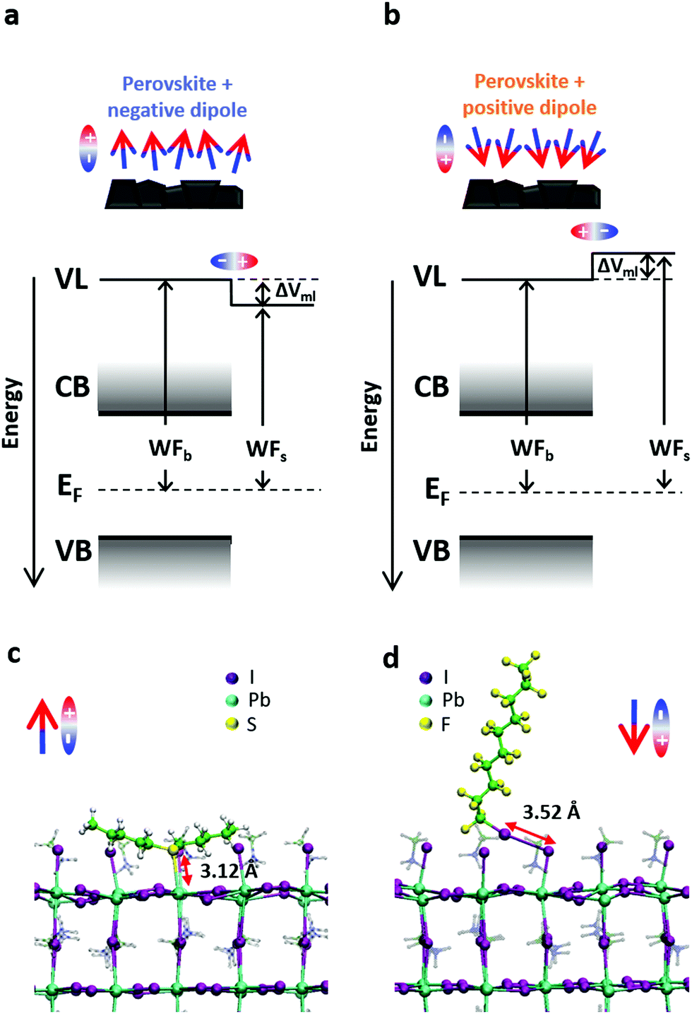 | ||
| Fig. 1 (a and b) Representation of the effect of the presence of a surface dipole on the perovskite band diagram for negative (a) and positive (b) dipoles. VL is the local vacuum level, ΔVml is the vacuum level shift induced by the dipolar monolayers, EF is the Fermi level energy, CB and VB are conduction and valence band, WFb is the bulk WF and WFs is the surface WF. (c and d) Representation of the coupling of the two main molecules employed in this work in the case of a 50%-MAI terminated/50% PbI2-terminated MaPbI3 perovskite, where MAI is methylammonium iodide. Specifically, in (c) amyl sulfide (csc5), binding to Pb ions of the surface and so representative of the negative dipole case. In (d) perfluorodecyl iodide (IPFC10), binding to the I ions on the surface and representative of the positive dipole case. | ||
On the other hand, a positive dipole will shift the vacuum level upwards, causing an increase in the WF of the functionalized material. In this case, we chose perfluorodecyl iodide (IPFC10 – Fig. 1c) as an example of the described behaviour. This molecule is already known in the literature for being able to form SAMs and enhance the efficiency and stability of perovskite solar cells.33,35 In this molecule, the iodine on the head remains slightly positive thanks to the electrons withdrawing effect of the fluorinated chain, which allows the molecule to behave like a Lewis acid and form halogen bond36–39 with the halogen ions on the perovskite surface.
The selective absorption of Lewis bases and Lewis acids makes them perfect candidates for generating a negative or positive dipole and, in our case, the main component of the total dipole seems to come from their interaction with the surface (see charge transfer analysis later in the text).
To demonstrate the scenario as mentioned above, we carried out various experimental and theoretical analyses. Making use of several techniques we measured WF and bands edges' position in the case of bare perovskite and perovskite functionalized with 10 mM solutions of the two molecules. We used a perovskite precursor solution with composition (Cs0.05[MA0.15FA0.85PbI0.85Br0.15]0.95).
At first, we measured several times with different UPS setups, but the results were repeatedly not reliable. We concluded that the molecules tend to detach in an ultra-high vacuum, making it challenging to draw actual conclusions from measurements in such conditions. For this reason, we decided to use other techniques working at atmospheric pressure, such as Kelvin probe (KP), Kelvin probe force microscopy (KPFM), Ambient Pressure Photoemission Spectroscopy (APS) and cyclic voltammetry (CV). We then compared the obtained results to ensure their reliability.
To evaluate the WF shift we performed KP40–43 measurements in different conditions (Fig. 2a): in one case the experiment was entirely done in air (dashed lines), in the other case the samples were quickly mounted in air, but the investigation was carried out in N2 atmosphere (solid lines). It is evident how the conditions of the measure can influence the amount of the shift. In both cases, samples treated with positive dipoles present an increase of the WF compared to the bare perovskite reference, while samples treated with negative dipoles show a WF decrease.
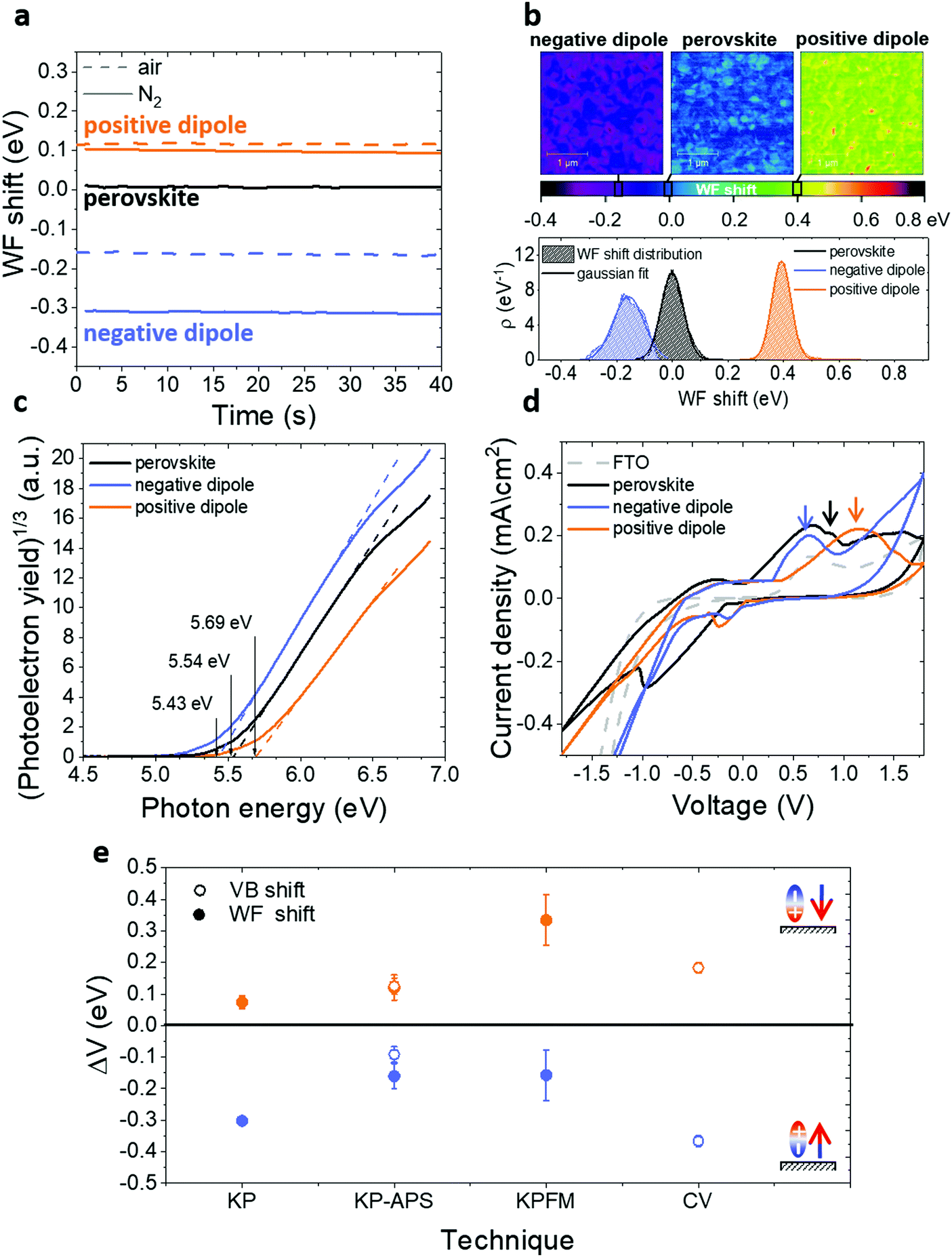 | ||
| Fig. 2 (a) WF shift due to the presence of interfacial dipoles measured with Kelvin probe (KP) in the dark in different environments: in one case (solid lines) the samples were measured in N2 but shortly exposed to air while mounting them on the setup, in the second case (dashed lines) the samples were mounted and measured in air. (b) Kelvin probe force microscopy (KPFM) WF shift maps in the case of bare perovskite and perovskite functionalized with positive and negative dipoles with corresponding distribution (ρ) plots. (c) Ambient Pressure Photoemission Spectroscopy (APS) plots of ITO/perovskite (black), ITO/perovskite/IPFC10 (orange), ITO/perovskite/csc5 (blue). Measurements performed in air. (d) Cyclic voltammetry (CV) of bare FTO (grey), FTO/perovskite (black), FTO/perovskite/IPFC10 (orange), FTO/perovskite/csc5 (blue). (e) Comparison of the WF shift and VB shift related to perovskite obtained with different techniques for the cases of a positive and negative dipole. | ||
To have a better idea of the real magnitude of the WF shift induced by the functionalization, we also performed KPFM43–45 measurements on non-air exposed samples. In Fig. 2b, we show the voltage maps of the WF shift for bare and functionalized perovskite together with the respective distributions. The results confirm the direction of the change already proven by KP and show a WF shift of about 150 meV for the negative dipole case and 300 meV for the positive dipole case. It is possible to notice that the distribution for the negative dipole functionalization is broader and less symmetric than the others, this might be an indication that at 10 mM concentration the surface is already saturated and in some areas, the molecules are packing in multilayers. This topic will be explored further in the following sections.
The maps also suggest that the shift is not homogeneous on the surface and the result is, therefore, an average of local WF variations. This behaviour is most likely due to the perovskite roughness and the presence of grains. In every map, the presence of small regions with a higher WF is indeed evident. Considering that our molecules functionalize the surface by binding to lead or halide ions, these regions probably indicate areas with a higher concentration of defects and thus higher concentration of molecules. According to the work of Gallet et al.,46 these regions might correspond to different facets of the crystalline structure. The local variation offers interesting data for further investigation. Nevertheless, it does not affect the results of this work, since the average gives the relevant quantity on a larger scale.
The KP setup operated in air is combined with an APS tool (KP-APS)42 in view to respectively determine the WF and the ionization energy (IE), i.e. the valence band maximum (VBM) relative to the local vacuum level on the same position over the sample. With the absolute WF and IE data measured, the KP-APS combination offers the possibility to determine the VBM shift and compare it with the WF shift under the same conditions. Fig. 2c shows the IE as determined from photoelectron yield spectroscopy plots in APS measurements and, as shown in Fig. 2e, the shifts of VBM and WF match in direction and magnitude for the different cases. This result is significant because it shows that both WF and VBM are shifting equally, and thus it allows to exclude the possibility that the detected WF shifts are due to doping of the perovskite layer. Therefore, this provides evidence that the surface dipole affects all the surface energetics of the perovskite.
Complementarily, we monitored the VB shift by performing CV on functionalized and bare perovskite on FTO (Fig. 2d), respectively. From the first distinguishable oxidation peaks of the different CV scans, it is possible to calculate the VB position by adding the redox potential of the Ag/AgCl electrode (4.65 eV)47 for the different cases. We can observe that the negative(positive) dipoles trigger a VB shift downwards(upwards) in relation to the VB of the reference perovskite on FTO. Both cases are comparable in direction and magnitude of VB shifts to those measured with the other techniques. The position of the reduction peaks in the range of the negative bias is instead not reliable because some partial perovskite degradation during the reverse scan was noted. Therefore, a calculation of the conduction band position is not possible in this case.
We do not have any direct measurement of the conduction band and its shift, but we measured the PL spectra of the different cases and, combining it with UV-Vis and EQE measurements (Fig. S9, ESI†), we calculated the bandgap. We obtained a value of approximately 1.64 eV and we could observe that it is independent of the functionalization. It follows that the conduction band is shifting in parallel of the valence band and WF.
In Fig. 2e we summarized the results. For all measurements conditions, we observed an increase(decrease) in WF and VB in the case of a positive(negative) dipole functionalization. Differences in absolute numbers are a consequence of varied measurement conditions inherent to the respective setups.
Having established that the dipolar molecules can control the positive and negative shift of the perovskite WF, we focused on achieving control over the magnitude of the change. We varied the concentration of the solution used for the deposition to control the distribution of the molecules on the perovskite surface and, consequently, the magnitude of the WF shift.
We measured the change in WF for the different solution concentrations through KP and KPFM, obtaining similar trends with both methods (Fig. S10, ESI†).
In Fig. 3a and b we show how the perovskite WF is changing depending on the solution concentration in the case of positive (3a) and negative (3b) dipole. In the positive dipole case (Fig. 3a), the work function is increasing with the increasing of the solution concentration until reaching saturation at about 40 mM. The two molecules (perfluorodecyl and perfluorododecyl iodide – IPFC10 and IPFC12) differ only in the chain length. Therefore the difference in the magnitude of the shift is due to the difference in the strength of the dipole, where the latter has a smaller dipole due to the higher molecular length (see ESI† for an overview of the dipoles of the used molecules and the charge transfer analysis).
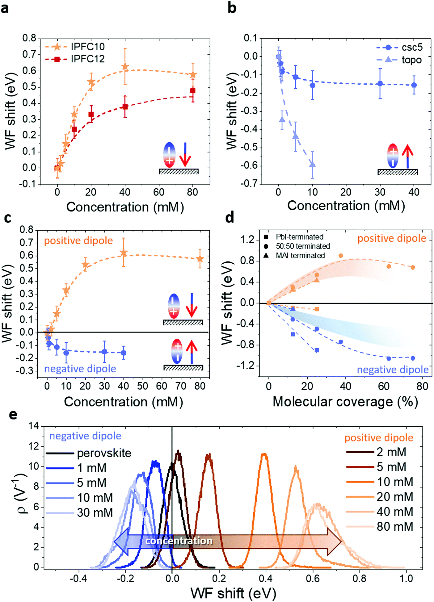 | ||
| Fig. 3 KPFM measurements showing the WF changing depending on the solution concentration when the perovskite is functionalized with a positive (a) and negative (b) dipole. In this specific case, the molecules creating a positive dipole were IPFC10 and IPFC12, and the ones making a negative dipole were csc5 and TOPO. (c) Comparison of the WF trends for the positive (orange) and negative (blue) dipole. (d) DFT simulations of the relation between WF shift and coverage for different surface terminations of MAPbI3, the shaded stripes represent the probable condition of the samples experimentally measured. (e) Distribution (ρ) of the WF shifts from KPFM measurements for different concentrations of negative and positive dipoles. The curves in (a)–(d) are spline fitting of the data. | ||
A similar trend is obtained in the case of a negative dipole (Fig. 3b), but with the WF decreasing compared to the perovskite one and reaching saturation already for a concentration of about 10 mM. In this case, the two molecules are different both in structure and binding group (amyl sulfide –csc5– and trioctylphosphine oxide –TOPO–), therefore we can state that it is the dipole type, not the specific molecule, which defines the direction of the shift and characteristics of the trend. In other words, the behaviour is independent of the molecule.
It is worth noting that TOPO-functionalized perovskite shows an extreme WF shift. Moreover, it was not possible to collect data for more than 10 mM concentration because for higher molarities the solution was damaging the perovskite film, presumably by dissolving the lead cations48 (Fig. S11, ESI†). This seems to suggest that TOPO might be a tricky molecule to use in devices, despite its excellent passivation properties reported by several papers.49–51
The above results show that by changing the solution concentration, it is possible to tune the magnitude of the WF shift up to several hundreds of meV. It is known that polar monolayers properties are determined not only by the type of molecules and bonding configuration to the substrate but also by size, (dis-)order and adsorption patterns within the monolayer.52,53 Therefore, in our opinion, the trends showed in Fig. 3 can be explained by considering the deposition kinetics, and it is related to the coverage. At first, all defect sites (i.e. Pb2+ and halide ions/vacancies) are free, consequently, as soon as the samples are immersed in the solution, the molecules start to bind to them. However, with low solution concentration, not all the defect sites can be occupied by a molecule, therefore the surface is not fully functionalized. With the increase of the concentration the functionalization level increases as well, until reaching a point where a molecule occupies all the surface defects, therefore the curves reach a plateau, and the condition for maximum WF shift is achieved. To be noted that a similar process would happen if the solution concentration were kept constant and the dipping time varied (see Fig. S14, ESI†), for this reason, it is crucial to keep one of these parameters fixed. In our case, we chose to settle the dipping time and vary the concentration, but we would like to stress that changing the dipping time would give the same results, since the process is related to the deposition kinetics of the molecules.
Another exciting feature is visible by comparing the trends for the positive and negative dipoles (Fig. 3c): the concentration at which the WF starts to saturate is different for the two cases. This behaviour may indicate a specific ratio of defects at the perovskite surface, in particular the ratio between halides and Pb vacancies. Indeed, in our case, the positive dipole is given by a Lewis acid, which is binding to the halides on the surface, while the negative dipole is provided by a Lewis base, which is binding to the Pb ions. Therefore, the fact that the negative dipole functionalization curve saturates at lower concentrations than the positive dipole curve suggests that there are less Pb ions on the surface compared to halide ions, i.e. there are more Pb vacancies. This result is in agreement with the work of Philippe et al.,54 where the I/Pb ratio at the surface for CsMAFA-perovskite is said to be around 3. Moreover, it is also essential to consider the geometry and the steric hindrance of the two molecules. Indeed, while IPFC10 consist of a straight-comparably rigid-chain which allows the molecules to form a compact vertical layer, csc5 has two aliphatic chains that most likely limits the number of molecules which can bind to the surface, thus leading earlier to saturation.
The difference in behaviour is also highlighted by the WF distribution curves in Fig. 3e (respective contact potential difference (CPD) maps in Fig. S12 and S13, ESI†). The negative dipole curve stops shifting and therefore reaches saturation for lower concentrations than the positive dipole one. Moreover, it is interesting to see how both curves start to broaden and lose symmetry while approaching saturation. This shows that initially (i.e. for low concentrations) the molecules are nicely depositing and forming an ordered monolayer. In contrast, with increasing concentration, the deposition seems to become less uniform, probably forming some agglomerates, especially when saturation is reached.
To support the experiments, we performed DFT simulations investigating the interaction of csc5 and IPFC10 with the MAPbI3 surface, here considered as the prototype lead halide perovskite (see computational details in ESI†). Molecule adsorption has been modelled on the (001) surface of tetragonal MAPbI3 in the supercell approach for three different terminations: (i) PbI2-terminated; (ii) 50%-MAI and 50% PbI2-terminated (half terminated); (iii) MAI-terminated, where MAI is methylammonium iodide. Initially, one and two molecules were absorbed on the PbI2, and MAI terminated slabs, corresponding to molecular coverages (θ) of 12.5% and 25%.
The adsorption energies and the associated WF shifts were monitored as a function of the molecular coverage and highlight a strong interaction between molecules and uncoordinated ions at the surface (see Table S3, ESI†). The adsorption of csc5 mainly occurs through the formation of an S–Pb bond at the surface with a bond length of ∼3.0 Å, and it is strongly predominant in the PbI2-terminated surface, while only slightly favored in the MAI-terminated surface.
On the other hand, IPFC10 mainly interact by forming halogen–halogen bonds with surface iodines at bond distances of ∼3.5 Å. Interestingly, on the PbI2-terminated surface IPFC10 adsorption results in the formation of both a Pb–I and an I–I bond, suggesting the simultaneous creation of a metal-halide and halogen bonds at distances of 3.3 and 3.5 Å, respectively (Fig. S4, ESI†).
We then investigated how the csc5 and IPFC10 adsorption influence the WF values for the different surface terminations (see Table S3 and Fig. S3, ESI†). Under all modelled terminations, the adsorption of csc5 leads to a WF reduction, while IPFC10 leads to a WF increase or, in one case, to a negligible decrease. In the PbI2-terminated case, the WF variations are particularly significant for csc5 adsorption, with a WF reduction of ca. 0.6 eV per single-molecule adsorption, while they are marginally influenced by IPFC10 adsorption. This is likely the result of the two different bonds (Pb–I and I–I) compensating each other. In the half terminated case csc5 still preferably interacts with Pb ions at the surface. At the same time, IPFC10 adsorption takes place exclusively through halogen bond, leading overall to a WF decrease (increase) of ca. 0.3 eV for csc5 (IPFC10) adsorption. A similar trend is reported on the fully passivated MAI-terminated surface and the same surface where an MAI vacancy was created for modelling the adsorption of csc5.
These results indicate that while csc5 preferentially interact with undercoordinated Pb atoms, leading to a WF decrease, IPFC10 can interact both with Pb or I surface atoms, forming different bonds whose contribution to the WF partially cancels out. However, a net WF increase is observed in the majority of the cases, including the one corresponding to our experimental data. Overall, under all considered adsorption situations, csc5 provides a WF reduction while IPFC10 leads mainly to a WF increase.
To understand the origin of the WF shift, we investigated the charge transfer between the adsorbed molecule and the surface in the different cases. The charge accumulation (depletion) upon the molecule adsorption has been evaluated by calculating the charge density difference between the molecule + slab system and the single components at fixed geometries (see Discussion and Fig. S5, S6 of ESI†). In the case of csc5, an accumulation of electronic charge is reported around the coordinated Pb at the surface and a charge depletion in the molecular region. The opposite is observed for the IPFC10 molecule, where depletion and accumulation of charge on Pb and the molecule, respectively, is reported on the half PbI2–MAI and MAI terminated surfaces. This is consistent with the formation of negative and positive dipoles at the interface for csc5 and IPFC10 molecules, respectively. An excellent correlation between the transferred charge at the molecule–surface interface and the computed WF shifts has also been found (Fig. S7, ESI†).
To investigate the effects of molecular coverage, we extended the simulations for the half terminated surface to high percentages of coverage, i.e. up to θ = 100%. In Fig. 3d the WF variation vs. θ is reported for csc5 and IPFC10 molecules. In both cases, the WF initially shifts almost linearly with the coverage and saturation of the WF shift for coverage higher than 40–50% is observed, in excellent agreement with the experimentally measured trends. Considering that the measurements were performed on CsMAFA-perovskite, our experimental results would be comparable with a situation in between half terminated surface and MAI-terminated surface (see shaded stripes in Fig. 3d). Naturally, variations between simulations and experiments also arise due to the different thermodynamics on the other surface of the grains and the presence of defects.
By comparing the trends in Fig. 3c and d for our conditions, we can notice how, in both cases, the WF shift has a higher magnitude for IPFC10. The numbers suggest that experimentally saturation is reached for a coverage of about 20% in the case of IPFC10 and 10% for csc5. As previously pointed out, this difference is most likely related to a smaller amount of Pb ions on the surface combined with a more significant steric hindrance of csc5.
Overall, the simulations support the correlation between surface coverage and WF shift and evidence the validity of this method to tune the perovskite WF in a controlled way.
So far, we showed how to obtain and control the WF shift induced by the functionalization. The next step is to investigate the effect on PSCs performance.
We prepared standard n–i–p devices, where the electron selective contact is given by compact and mesoporous TiO2, and the hole selective contact is the widely used spiro-OMeTAD. We functionalized the perovskite with different concentrations of csc5 to create a negative dipole at the interface and modify in this way the energy level alignment. The expected effect of the dipolar functionalization is to reduce the approximately 200 meV offset between the perovskite valence band and the spiro-OMeTAD HOMO level.
Specifically, we explored the effect of functionalization with a low concentration (0.5 mM), meaning a WF shift of about 40 meV, and with high concentration (10 mM), which represent already a situation of surface saturation and should give a WF shift of approximately 160 meV.
In Fig. 4 we can see how the photovoltaic (PV) parameters such as open-circuit voltage (Voc), short-circuit current (Jsc), fill factor (FF) and photovoltaic conversion efficiency (PCE) are changing. We observe that the Voc is increasing with increasing concentration, while the FF remains almost constant after the initial improvement and the Jsc do not change significantly.
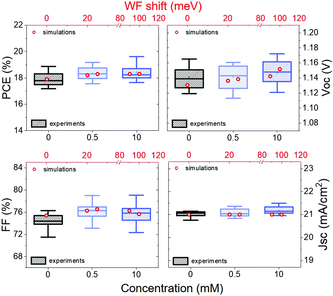 | ||
| Fig. 4 PCE, Voc, FF and Jsc of n–i–p devices with structure FTO/TiO2 (compact and mesoporous)/perovskite/csc5/spiro-OMeTAD/Au for different values of negative WF shift. The box charts are the values obtained experimentally from J–V curves measured at 0.01 V s−1, while the red circles represent how the PV parameters change depending on the WF shift according to drift-diffusion simulations. | ||
When the perovskite surface is functionalized with dipoles, there are different factors which can affect the devices' PV parameters. The dipoles induce a change in energy level alignment, but at the same time, there is evidence that they can have a passivating effect.55 Besides, the molecules are binding to defects on the perovskite surface, reducing in this way the trap states. It is therefore difficult to disentangle the effect of the different factors. Thus we performed drift-diffusion simulations to gain a better insight.
In the simulations, one of the current density–voltage (J–V) curves from our control devices was set as a reference. Then only the perovskite energetics and the recombination time were varied to simulate the presence of a negative dipole at the interface between perovskite and spiro-OMeTAD. The results are represented by the red circles in Fig. 4.
The simulations show that the experimental trend is reproducible considering smaller WF shifts than those measured with KPFM and increasing the recombination time constant at the interface from 1.6 × 10⁻¹⁰ s to 2.84 × 10⁻¹⁰ s. In particular, the simulations predict a WF shift of about 25 meV for devices functionalized with a 0.5 mM solution and 100 meV for the 10 mM case. This seems to indicate that part of the deposited molecules are lost in the devices making process, leading to a smaller WF shift and therefore also to just a slight reduction on the perovskite – spiro-OMeTAD offset.
Both experimental data and simulations show an initial increase in FF, which can be ascribed to a better charge extraction due to a reduced perovskite – spiro-OMeTAD offset. It is also possible to observe a small loss in FF while passing from 0.5 mM to 10 mM, while the Voc keeps increasing. As already discussed before, it is possible that at saturation concentration (i.e. 10 mM in this case) the molecules layer is not uniform, agglomerates might act as insulators and partially reduce the charge transport, leading to a reduction of the FF. The Voc increase is instead consistent with an improvement in energy level alignment and with suppression of recombination. There is evidence that the latter could also be related to the presence of an electric field generated by the dipoles, which can push away the electrons from the interface.55 It is also worth highlighting the consistency of this behaviour with the results from a previous work employing IPFC10 at the interface between perovskite and C60 in n–i–p PSCs,35 where a similar Voc trend was observed. Moreover, it is demonstrated that Voc in PSCs tends to increase with the strength of the chemical bonding between perovskite and the deposited molecules,56 that is similar to our case, in which a higher molecules concentration leads to more significant WF shift.
We can also see that the simulations do not predict a change in Jsc, while experimentally, we observe a small variation. Nevertheless, it is quite common in perovskite solar cells to have Jsc fluctuation of about ±0.5 mA cm−2 even for identical devices. Therefore we do not consider this change significant.
Overall, the simulations show the effect of interfacial dipoles and the WF shifts on PSCs and highlight that the behaviour observed experimentally can be justified by considering only the influence of the dipoles. It is also worth noticing that the actual WF shift in the device seems to be about half of the nominal value, which is a factor to take into consideration for future experiments.
These results suggest that the presence of a dipolar layer at the interface between perovskite and transport layers can influence and, if the conditions are appropriately chosen, improve the energy level alignment in PSCs. There is, therefore, great potential in the application of this technique for fine adjustment of the energy level alignment at interfaces or for simply tuning the perovskite energetics.
Conclusions
In conclusion, we managed to control the deposition of dipolar self-assembled monolayers (SAMs) on halide perovskite and obtain this way a controlled shift of perovskite work function, valence and conduction bands. We can control the direction of the shift with the direction of the surface dipoles and we can control the magnitude of the shift by tuning the density of the surface dipoles. We were able to shift the perovskite WF up to several hundreds of meV, and we explored the effect of this approach on PSCs with the support of experimental and simulated data.Our work showed that tuning the work function of semiconductors through surface functionalization with dipolar molecules, which is a well known method in organic and inorganic semiconductor physics, can be extended to hybrid organic–inorganic perovskite semiconductors. These findings provides a new toolbox to enhance further the flexibility of applying halide perovskites in optoelectronics.
Conflicts of interest
There are no conflicts to declare.Acknowledgements
L. C. thanks Dr. Thomas Dittrich (KP setup), Carolin Rehermann (UV-Vis) and Dr. Aboma Merdasa (PL) for the measurements and the many useful discussions. L. C., A. A., and P. V. thank Forschungszentrum Jülich GmbH and Business Finland (SolarWAVE project) for financial support. The work is part of the Academy of Finland Flagship Programme, Photonics Research and Innovation (PREIN), decision 320165. L. C. and N. P. thank HyPerCells graduate school, organized jointly by the University of Potsdam and HZB. A. S. and A. G. thank TUM International Graduate School of Science and Engineering (IGSSE), and the German Academic Exchange Service (DAAD).References
- A. Ciavatti, L. Basiricò, I. Fratelli, S. Lai, P. Cosseddu, A. Bonfiglio, J. E. Anthony and B. Fraboni, Adv. Funct. Mater., 2019, 1806119, 1–8 Search PubMed
.
- M. Stössel, J. Staudigel, F. Steuber, J. Simmerer and A. Winnacker, Appl. Phys. A, 1999, 390, 387–390 Search PubMed
- Y. Wang, T. Zhang, M. Kan, Y. Li, T. Wang and Y. Zhao, Joule, 2018, 1–11 Search PubMed
- P. Schulz, E. Edri, S. Kirmayer, G. Hodes, D. Cahen and A. Kahn, Energy Environ. Sci., 2014, 1377–1381 RSC
- Best Research Cell Efficiencies (https://www.nrel.gov/pv/assets/pdfs/best-research-cell-efficiencies.20191106.pdf).
- T. Song, Q. Chen, H. Zhou, C. Jiang, H. Wang, M. Yang and Y. Liu, J. Mater. Chem. A, 2015, 3, 9032–9050 RSC
-
D. B. Mitzi, I. B. M. T. J. Watson, I. Box and D. B. Mitzi, Synthesis, Structure, and Properties of Organic–Inorganic Perovskites and Related Materials, 1999 Search PubMed
- C. Zuo, H. J. Bolink, H. Han, J. Huang and D. Cahen, Adv. Sci., 2016, 1–16 Search PubMed
- J. Chen, X. Cai, D. Yang, D. Song, J. Wang, J. Jiang, A. Ma, S. Lv, M. Z. Hu and C. Ni, J. Power Sources, 2017, 355, 98–133 CrossRef CAS
- K.-G. Lim, S. Ahn and T.-W. Lee, J. Mater. Chem. C, 2018, 2915–2924 RSC
- T. Yajima, Y. Hikita, M. Minohara, C. Bell, J. A. Mundy, L. F. Kourkoutis, D. A. Muller, H. Kumigashira, M. Oshima and H. Y. Hwang, Nat. Commun., 2015, 6, 1–5 Search PubMed
- M. Ye, C. He, J. Iocozzia, X. Liu, X. Cui, X. Meng, M. Rager, X. Hong, X. Liu and Z. Lin, J. Phys. D: Appl. Phys., 2017, 50(37) DOI:10.1088/1361-6463/aa7cb0
- E. Zojer, T. C. Taucher and O. T. Hofmann DOI:10.1002/admi.201900581.
- P. Zhao, B. J. Kim and H. S. Jung, Mater. Today Energy, 2018, 7, 267–286 CrossRef
- B. De Boer, A. Hadipour, M. M. Mandoc, T. Van Woudenbergh and P. W. M. Blom, Adv. Mater., 2005, 17, 621–625 CrossRef CAS
- X. Zhang, Y. Sun, M. Wang, H. Cui, W. Xie, L. Shen and W. Guo, Sol. Energy, 2019, 181, 9–16 CrossRef CAS
- Y. Yang, C. Liu, Y. Ding, Z. Arain, S. Wang, X. Liu, T. Hayat, A. Alsaedi and S. Dai, ACS Appl. Mater. Interfaces, 2019, 11, 34964–34972 CrossRef CAS
- D. Liu, H. Zheng, Y. Wang, L. Ji, H. Chen, W. Yang, L. Chen, Z. Chen and S. Li, Chem. Eng. J., 2020, 125010 CrossRef CAS
- A. Agresti, A. Pazniak, S. Pescetelli, A. Di Vito, D. Rossi, A. Pecchia, M. Auf der Maur, A. Liedl, R. Larciprete, D. V. Kuznetsov, D. Saranin and A. Di Carlo, Nat. Mater., 2019, 18, 1228–1234 CrossRef CAS
- Z. Wu, Z. Liu, Z. Hu, Z. Hawash, L. Qiu, Y. Jiang, L. K. Ono and Y. Qi, Adv. Mater., 2019, 1804284, 1–7 Search PubMed
- H. Dong, J. Xi, L. Zuo, J. Li, Y. Yang, D. Wang, Y. Yu, L. Ma, C. Ran, W. Gao, B. Jiao, J. Xu, T. Lei, F. Wei, F. Yuan, L. Zhang, Y. Shi, X. Hou and Z. Wu, Adv. Funct. Mater., 2019, 1808119, 1808119 CrossRef
- I. H. Campbell, J. D. Kress, R. L. Martin, D. L. Smith and N. N. Barashkov, Appl. Phys. Lett., 1997, 3528, 1–4 Search PubMed
- I. H. Campbell, S. Rubin, T. A. Zawodzinski, J. D. Kress, R. L. Martin, D. L. Smith, N. N. Barashkov and J. P. Ferraris, Phys. Rev. B, 1996, 54, 321–324 CrossRef
- D. M. Alloway, M. Hofmann, D. L. Smith, N. E. Gruhn, A. L. Graham, R. Colorado, V. H. Wysocki, T. R. Lee, P. A. Lee and N. R. Armstrong, J. Phys. Chem. B, 2003, 107, 11690–11699 CrossRef CAS
- O. Zenasni, A. C. Jamison and T. R. Lee, Soft Matter, 2013, 9, 6356–6370 RSC
- W. E. Ford, D. Gao, N. Knorr, R. Wirtz, F. Scholz, Z. Karipidou, K. Ogasawara, S. Rosselli, V. Rodin, G. Nelles and F. Von Wrochem, ACS Nano, 2014, 8, 9173–9180 CrossRef CAS
- I. Lange, S. Reiter, M. Pätzel, A. Zykov, A. Nefedov, J. Hildebrandt, S. Hecht, S. Kowarik, C. Wöll, G. Heimel and D. Neher, Adv. Energy Mater., 2014, 1–11 Search PubMed
- M. Raoufi and D. Neher, Phys. Status Solidi, 2020, 217(5) DOI:10.1017/CBO9781107415324.004
- W. Kong, W. Li, C. Liu, H. Liu, J. Miao, W. Wang, S. Chen, M. Hu, D. Li, A. Amini, S. Yang, J. Wang, B. Xu and C. Cheng DOI:10.1021/acsnano.8b07627.
- R. Zhang, W. Liu, R. Hu, Y. Ma, Y. Sun, J. Zhang, Y. Pu, J. Yang, L. Chu and X. Li, Sol. Energy Mater. Sol. Cells, 2019, 191, 183–189 CrossRef CAS
- S. Sadhu, K. Aqueche, T. Buffeteau, J. M. Vincent, L. Hirsch and D. M. Bassani, Mater. Horiz., 2019, 6, 192–197 RSC
- A. Abate, M. Saliba, D. J. Hollman, S. D. Stranks, K. Wojciechowski, R. Avolio, G. Grancini, A. Petrozza and H. J. Snaith, Nano Lett., 2014, 14, 3247–3254 CrossRef CAS
- A. Abate, R. Dehmel, A. Sepe, N. L. Nguyen, B. Roose, N. Marzari, J. K. Hong, J. M. Hook, U. Steiner and C. Neto, J. Mater. Chem. A, 2019, 7, 24445–24453 RSC
-
G. N. Lewis, Valence and the Structure of Atoms and Molecules, 1923 Search PubMed
- C. M. Wolff, L. Canil, C. Rehermann, N. N. Linh, P. Caprioglio, L. Fiedler, M. Stolterfoht, A. Abate and D. Neher, ACS Nano DOI:10.1021/acsnano.9b03268
- G. Cavallo, P. Metrangolo, R. Milani, T. Pilati, A. Priimagi, G. Resnati and G. Terraneo, Chem. Rev., 2016, 116, 2478–2601 CrossRef CAS
- S. Bi, H. Wang, J. Zhou, S. You, Y. Zhang, X. Shi, Z. Tang and H. Zhou, J. Mater. Chem. A, 2019,(12) 10.1039/C8TA11835C
- G. R. Desiraju, P. S. Ho, L. Kloo, A. C. Legon, R. Marquardt, P. Metrangolo, P. Politzer, G. Resnati and K. Rissanen, Pure Appl. Chem., 2013, 85, 1711–1713 CAS
- R. Gutzler, C. Fu, A. Dadvand, Y. Hua, J. M. MacLeod, F. Rosei and D. F. Perepichka, Nanoscale, 2012 10.1039/c2nr31648j
- L. Kelvin, Philos. Mag. Ser. 5, 1898, 46, 82–120 CrossRef
- W. A. Zisman DOI:10.1063/1.1748947 .
- J. R. Harwell, T. K. Baikie, I. D. Baikie, J. L. Payne, C. Ni, J. T. S. Irvine, G. A. Turnbull and I. D. W. Samuel, Phys. Chem. Chem. Phys., 2016, 18, 19738–19745 RSC
- C. Musumeci, A. Liscio, V. Palermo and P. Samorì, Mater. Today, 2014, 17, 504–517 CrossRef CAS
- M. Nonnenmacher, M. P. O. Boyle, H. K. Wickramasinghe and M. Nonnenmacher, Appl. Phys. Lett., 1991, 2921(58) DOI:10.1063/1.105227
- Z. Kang, H. Si, M. Shi, C. Xu, W. Fan and S. Ma, Sci. China Mater., 2019, 1–14 Search PubMed
- T. Gallet, D. Grabowski, T. Kirchartz and A. Redinger, Nanoscale, 2019 10.1039/C9NR02643F
-
A. M. Bond, R. G. Compton, D. A. Fiedler, G. Inzelt, H. Kahlert, H. Lohse, M. Lovric, S. K. Lovric, F. Marken, A. Neudeck, U. Retter, F. Scholz and Z. Stojek, Electroanalytical Methods Guide to Experiments and Applications, 2nd, revised and extended edn, 2009 Search PubMed
- G. E. Eperon and D. S. Ginger, ACS Energy Lett., 2017, 2, 1190–1196 CrossRef CAS
- R. A. Belisle, K. A. Bush, L. Bertoluzzi, A. Gold-parker, M. F. Toney and M. D. Mcgehee, ACS Energy Lett., 2018, 3, 2694–2700 CrossRef CAS
- D. W. Dequilettes, S. Koch, S. Burke, R. K. Paranji, A. J. Shropshire, M. E. Ziffer and D. S. Ginger, ACS Energy Lett., 2016, 1, 438–444 CrossRef CAS
- I. L. Braly, D. W. Dequilettes, L. M. Pazos-Outón, S. Burke, M. E. Ziffer, D. S. Ginger and H. W. Hillhouse, Nat. Photonics, 2018, 12, 355–361 CrossRef CAS
- N. Gozlan, U. Tisch and H. Haick, J. Phys. Chem. C, 2008, 112(33), 12988–12992 CrossRef CAS
- Y. Yang, J. Zhou, M. Nakayama, L. Nie, P. Liu and M. G. White, J. Phys. Chem. C, 2014, 118, 13697–13706 CrossRef CAS
- B. Philippe, M. Saliba, J. P. Correa-Baena, U. B. Cappel, S. H. Turren-Cruz, M. Grätzel, A. Hagfeldt and H. Rensmo, Chem. Mater., 2017, 29, 3589–3596 CrossRef CAS
- F. Ansari, E. Shirzadi, M. Salavati-niasari, T. Lagrange, K. Nonomura, J. Yum, K. Sivula, S. M. Zakeeruddin, M. K. Nazeeruddin, M. Grätzel, P. J. Dyson and A. Hagfeldt DOI:10.1021/jacs.0c01704.
- J. Xie, K. Yan, H. Zhu, G. Li, H. Wang, H. Zhu, P. Hang, S. Zhao, W. Guo, D. Ye, L. Shao, X. Guan, T. O. Ngai, X. Yu and J. Xu, Sci. Bull., 2020, 65(20) DOI:10.1016/j.scib.2020.05.031
Footnote |
| † Electronic supplementary information (ESI) available. See DOI: 10.1039/d0ee02216k |
| This journal is © The Royal Society of Chemistry 2021 |