
 Open Access Article
 This Open Access Article is licensed under a Creative Commons Attribution-Non Commercial 3.0 Unported Licence
Highly conductive and stable Co9S8 thin films by atomic layer deposition: from process development and film characterization to selective and epitaxial growth†
Miika
Mattinen‡
 a,
Timo
Hatanpää
a,
Kenichiro
Mizohata
b,
Jyrki
Räisänen
b,
Markku
Leskelä
a and
Mikko
Ritala
*a
a,
Timo
Hatanpää
a,
Kenichiro
Mizohata
b,
Jyrki
Räisänen
b,
Markku
Leskelä
a and
Mikko
Ritala
*a
aDepartment of Chemistry, University of Helsinki, P.O. Box 55, FI-00014, Finland. E-mail: mikko.ritala@helsinki.fi
bDepartment of Physics, University of Helsinki, P.O. Box 43, FI-00014, Finland
First published on 20th August 2021
Abstract
Co9S8 is an interesting sulfide material with metallic conductivity that has shown promise for various energy applications. Herein, we report a new atomic layer deposition process producing crystalline, pure, and highly conductive Co9S8 thin films using CoCl2(TMEDA) (TMEDA = N,N,N′,N′-tetramethylethylenediamine) and H2S as precursors at 180–300 °C. The lowest resistivity of 80 μΩ cm, best uniformity, and highest growth rate are achieved at 275 °C. Area-selective deposition is enabled by inherent substrate-dependency of film nucleation. We show that a continuous and conductive Co9S8 film can be prepared on oxide-covered silicon without any growth on Si–H. Besides silicon, Co9S8 films can be grown on a variety of substrates. The first example of an epitaxial Co9S8 film is shown using a GaN substrate. The Co9S8 films are stable up to 750 °C in N2, 400 °C in forming gas, and 225 °C in O2 atmosphere. The reported ALD process offers a scalable and cost-effective route to high-quality Co9S8 films, which are of interest for applications ranging from electrocatalysis and rechargeable batteries to metal barrier and liner layers in microelectronics and beyond.
Introduction
Cobalt forms a range of crystalline sulfides, including cubic Co4S3, cubic Co9S8 (mineral name cobalt pentlandite), hexagonal CoS (jaipurite), cubic Co3S4 (linnaeite), and cubic CoS2 (cattierite).1–3 Co9S8 displays metallic conductivity and it is one of the most studied and stable cobalt sulfide phases. Co9S8 has been actively explored as an electrode for electrocatalytic water splitting including both oxygen evolution reaction (OER)4–6 and hydrogen evolution reaction (HER),5,7,8 as well as for lithium ion batteries,9 zinc-air batteries,6 dye-sensitized solar cells,10–12 and supercapacitors.13,14 Due to its high conductivity and stability, Co9S8 may also be of interest as a barrier and liner layer for interconnects in microelectronics, provided that ultrathin continuous films can be prepared. This possibility seems particularly interesting in light of Intel's introduction of cobalt interconnects at the 10 nm node.15To date, several methods have been used to deposit Co9S8 nanoparticles, including colloidal synthesis,5,11 solvothermal16 and hydrothermal synthesis,4 thermal decomposition,17 and spray pyrolysis.18 Rough thin films from hundreds of nanometers to micrometers in thickness have been prepared by chemical vapor deposition (CVD),19–21 electrodeposition,9,12 and solvothermal synthesis.7,10
The aforementioned methods have, however, struggled in producing thin, continuous Co9S8 thin films with accurately controlled, uniform thickness and high material quality. To overcome these limitations, we use atomic layer deposition (ALD), which is an advanced modification of CVD. In ALD, alternately pulsed precursors react with the substrate one-by-one in self-limiting manner, while the reactor is purged between the precursor pulses to ensure that the precursors do not react with each other in the gas phase.22–24 Each ALD cycle deposits a (sub)monolayer of material, which gives ALD unmatched control over film thickness, uniformity, and conformality on both large and three-dimensional substrates. Excellent scalability, reproducibility, and relatively low deposition temperatures from room temperature to about 500 °C are also important characteristics of ALD. The unique advantages of ALD have led to its widespread industrial use.25,26 ALD can be used to deposit numerous materials,27 including elements, oxides, and nitrides, as well as many sulfides.28 However, when developing an ALD process for a new material, it is often a challenge to identify molecules that fulfill the demanding requirements set for an ALD precursor, including volatility, high reactivity, and lack of self-decomposition pathways at the deposition temperature.
So far, only one ALD process exists for Co9S8, which uses Co(iPrAMD)2 and H2S at 100–225 °C.6,8,13,14,29 In addition, the same Co(iPrAMD)2 precursor has been used with H2S plasma to deposit CoS2 thin films at 80–225 °C.30 However, Co(iPrAMD)2 is an expensive precursor (∼200 eur g−1),31 which limits its use for large-scale applications. Furthermore, the resistivity of the Co9S8 films deposited by this process is relatively high, 3–5 mΩ cm.13
CoCl2(TMEDA) (TMEDA = N,N,N′,N′-tetramethylethylenediamine) was recently introduced as an affordable alternative to existing cobalt ALD precursors. Its favorable ALD precursor characteristics have been shown for deposition of high-quality CoO (ref. 32) and Co3Sn2 (ref. 33 and 34) thin films. In this article, CoCl2(TMEDA) is used with H2S to deposit crystalline Co9S8 films with a low resistivity on the order of 100 μΩ cm. Detailed investigation of the ALD process at temperatures ranging from 180 to 300 °C is followed by characterization of morphology, crystallinity, resistivity, and composition of the deposited films. Film nucleation and growth on different substrates is also studied in detail to assess the potential of the process for area-selective and epitaxial growth as well as compatibility with different substrates. Finally, high-temperature XRD measurements are used to evaluate the stability and applicability of the films in harsh conditions.
Experimental
Film deposition
Cobalt sulfide thin films were deposited using a commercial, hot-wall, cross-flow ALD reactor (F120, ASM Microchemistry) operated under approximately 5 mbar pressure.35 Nitrogen (N2, 99.999%, AGA) was further purified using a SAES Microtorr MC1-902F purifier and was used as the carrier and purge gas at a flow rate of 400 sccm. Dichloro(N,N,N′,N′-tetramethylethylenediamine)cobalt(II) [CoCl2(TMEDA)] precursor was synthesized in house using a simple one-step room temperature route giving 99% yield.32 The precursor was heated to 170 °C in an open boat held inside the ALD reactor and pulsed by inert gas valving. The precursor is a solid at room temperature, but it melts under the source conditions used in this work. The mildly air sensitive precursor was stored and handled in a N2 glove box before transferring to the ALD reactor.The sulfur precursor hydrogen sulfide (H2S, 99.5%, Linde) was further purified using a SAES Microtorr MC1-302F purifier. The flow rate of H2S was set to 14 sccm under a continuous flow using a mass flow meter and a needle valve and it was pulsed into the reactor using an external solenoid valve.
Caution! Safe use of highly toxic and flammable H2S gas requires a properly designed ALD reactor and laboratory space. The H2S bottle was stored in a ventilated gas cabinet and the H2S lines were designed to be compatible with H2S, using VCR metal and EPDM polymer seals. The reactor exhaust was bubbled through aqueous Cu(NO3)2 solution to remove H2S downstream of the vacuum pump. An example of ALD reactor modifications for H2S has been published by Dasgupta et al.36
Cobalt sulfide films were mostly deposited on 5 × 5 cm2 Si(100) and soda lime glass (SLG) substrates. The Si substrates were used as supplied with a native oxide layer. The SLG substrates were cleaned using successive ultrasonic baths of an alkaline detergent (Industrial Strength Cleaner, Branson), tap water, ethanol, and deionized water (10 minutes each, room temperature) followed by careful rinsing using deionized water and 50![[thin space (1/6-em)]](https://www.rsc.org/images/entities/char_2009.gif) :50 (v/v%) deionized water/ethanol solution and blown dry using pressurized air. Smaller pieces of other substrates were used for selected depositions, including thermal SiO2 (300 nm)/Si, Si–H(100), sapphire (2′′ wafer, C-plane off to M-plane by 0.2 ± 0.1°, double-side polished, University Wafer), muscovite mica (15 mm disks, V1 grade, Nano-Tec), GaN (epitaxially grown on Si(111) by MOCVD with an AlN nucleation layer and AlGaN buffer layers at Imec, see Fig. S21 in the ESI†), and different ALD films (Al2O3, Ir, and TiO2) prepared in-house on Si. Muscovite mica was cleaved using a double-edged razor blade immediately before deposition to reveal a fresh (001) surface.37 Sapphire wafers were rinsed with ethanol, acetone, and isopropanol followed by annealing in air at 1000 °C for 2 h to create a surface consisting of flat (0001) terraces.38 Si–H was prepared by dipping a silicon(100) substrate with a native oxide into a 1 v% aqueous HF solution for 2 min followed by rinsing with deionized H2O, blowing dry with pressurized N2, and loading into the reactor. The other substrates were stored in air and blown clean of particles using pressurized N2.
:50 (v/v%) deionized water/ethanol solution and blown dry using pressurized air. Smaller pieces of other substrates were used for selected depositions, including thermal SiO2 (300 nm)/Si, Si–H(100), sapphire (2′′ wafer, C-plane off to M-plane by 0.2 ± 0.1°, double-side polished, University Wafer), muscovite mica (15 mm disks, V1 grade, Nano-Tec), GaN (epitaxially grown on Si(111) by MOCVD with an AlN nucleation layer and AlGaN buffer layers at Imec, see Fig. S21 in the ESI†), and different ALD films (Al2O3, Ir, and TiO2) prepared in-house on Si. Muscovite mica was cleaved using a double-edged razor blade immediately before deposition to reveal a fresh (001) surface.37 Sapphire wafers were rinsed with ethanol, acetone, and isopropanol followed by annealing in air at 1000 °C for 2 h to create a surface consisting of flat (0001) terraces.38 Si–H was prepared by dipping a silicon(100) substrate with a native oxide into a 1 v% aqueous HF solution for 2 min followed by rinsing with deionized H2O, blowing dry with pressurized N2, and loading into the reactor. The other substrates were stored in air and blown clean of particles using pressurized N2.
Film characterization
Film morphology was examined by scanning electron microscopy (SEM, Hitachi S-4800) and atomic force microscopy (AFM, Veeco Multimode V). Tapping mode AFM imaging was performed in air using silicon probes with a nominal radius of less than 10 nm (Bruker). The images were flattened with no other image processing performed. Roughness was calculated as a root-mean-square (Rq) value.Film thicknesses were measured by energy-dispersive X-ray spectrometry (EDS, Oxford INCA 350 connected to the Hitachi S-4800 SEM). GMRFilm software39 was used to convert the measured Co and S Kα k-ratios to film thicknesses assuming bulk density of Co9S8 (5.34 g cm−3).40 X-ray reflectivity (XRR, Rigaku SmartLab) was also used for thickness measurements. XRR was mostly used for films thinner than approximately 15 nm and EDS for films thicker than 15 nm. Reliable use of EDS for thinner films was prevented by low signal intensity, whereas the high roughness of thicker films prevented accurate XRR measurements of them.
EDS was also used to measure the S/Co ratio of the films, while complete elemental composition was analyzed by time-of-flight elastic recoil detection analysis (ToF-ERDA) using 40 MeV 127I7+ ion beam. The angle between the incident beam and sample surface was 16° and that between the recoiled beam and sample surface was 24°, resulting in 40° incident beam to detector angle. The film surface and film/substrate interfaces were excluded when evaluating the compositions from the ToF-ERDA results.
Sheet resistance was measured by a four-point-probe (CPS Probe station connected to a Keithley 2400 SourceMeter). The sheet resistance was converted to resistivity using the thicknesses measured by EDS or XRR.
Crystallinity was studied by X-ray diffraction (XRD, Rigaku SmartLab) in either grazing incidence (GIXRD, ω = 1°) or θ − 2θ geometry. In addition, rocking curve (ω scan) measurements were used to quantify out-of-plane texture. Epitaxial in-plane registration of the films grown on mica and GaN was studied using in-plane pole figure and in-plane φ scan (incident angle 0.3°) measurements with the diffraction angle (denoted 2θB and 2θχ in these measurements, respectively) fixed to known substrate and film reflections.41,42 The diffractometer was equipped with an in-plane arm and a non-monochromatized copper X-ray tube mainly emitting Cu Kα radiation (λ ≈ 1.54 Å, consisting of Cu Kα1 and Kα2 at 1.5406 and 1.5443 Å). Minor contributions from Cu Kβ (λ ≈ 1.39 Å) and W Lα (λ ≈ 1.48 Å) lines were also present, which is apparent especially in the strongest substrate reflections. A Rigaku D/Tex Ultra 250 detector was used to suppress the high fluorescent background originating from cobalt in the films.
Thermodynamic calculations and visualization of epitaxy
Thermodynamic calculations of deposition chemistry were done using Outokumpu HSC Chemistry for Windows software (version 5.11).VESTA software43 was used to visualize the orientation of Co9S8 on GaN using data from the Inorganic Crystal Structure Database (ICSD; Co9S8 no. 23929, GaN no. 54698).
High-temperature X-ray diffraction
In situ high-temperature XRD (HTXRD) measurements were performed using an Anton-Paar HTK1200N oven connected to a PANalytical X'Pert Pro MPD diffractometer employing a non-monochromatized copper X-ray tube in grazing incidence (ω = 1°) geometry. For each measurement, either an laboratory air (1 atm), O2 (1 atm, AGA, 99.999%), N2 (30 mbar achieved by a diaphragm pump, AGA, 99.999%, further purified using an Entegris Gatekeeper purifier), or forming gas (1 atm, 10% H2 in N2, AGA) or dynamic vacuum (approximately 10−5 mbar achieved by a turbomolecular pump backed by a diaphragm pump) was used. The studied Co9S8 films (deposited on Si(100) at 275 °C using 1000 cycles) were first heated from room temperature up to the starting temperature of 100 or 125 °C at a heating rate of 10 °C min−1. Thereafter, a diffractogram was recorded every 25 °C, which took 27 min at each temperature, before heating to the next temperature at a heating rate of 10 °C min−1. The measurements were continued up to 725 or 750 °C, resulting in a total measurement time of approximately 15 h per experiment.Results and discussion
Film deposition
Cobalt sulfide thin films were deposited by ALD using alternating pulses of CoCl2(TMEDA) and H2S separated by nitrogen purge steps. Initial deposition studies showed that Co9S8 films could be deposited in the whole available temperature range of 180 to 300 °C. The lower temperature limit was dictated by the CoCl2(TMEDA) source temperature of 170 °C and the higher limit by the onset of CoCl2(TMEDA) decomposition.32 The neutral TMEDA adduct ligand makes the non-volatile cobalt(II) chloride volatile, while it has little effect on the deposition chemistry.32,34 Thermodynamically, the reactions between CoCl2 and H2S producing cobalt sulfide in different possible stoichiometries (Co9S8, CoS, Co3S4, and CoS2) are favorable with similar ΔG values of approximately −125 to −145 kJ mol−1 of CoCl2 at 180–300 °C (section S1 in the ESI†). Thus, the corresponding ALD surface reactions of our process are also likely to be very favorable.Next, the self-limiting nature of the surface reactions, a unique characteristic of ALD, was assessed. With increasing CoCl2(TMEDA) pulse time, the growth rate appeared to saturate at 180 °C to approximately 0.2 Å per cycle when a pulse length of at least 1.0 s was used (Fig. 1a). At 250 °C, the growth rate was doubled to approximately 0.4 Å per cycle using pulse lengths of 0.5 to 2.0 s. At 275 °C, the growth rate was clearly higher, for example 0.7 Å per cycle using 1.0 s CoCl2(TMEDA) pulses. Increasing the CoCl2(TMEDA) pulse length at 275 °C led to an increase of the growth rate, reaching 1.0 Å per cycle using 4.0 s pulses. No complete saturation was observed even with 8.0 s pulses, although the increase in the growth rate slowed down with the longest pulses tested (ESI, Fig. S2†). However, no film growth was observed when only CoCl2(TMEDA) was pulsed repeatedly at 275 °C on silicon or on an ALD-grown cobalt sulfide film (ESI, Fig. S3†), ruling out decomposition of CoCl2(TMEDA).
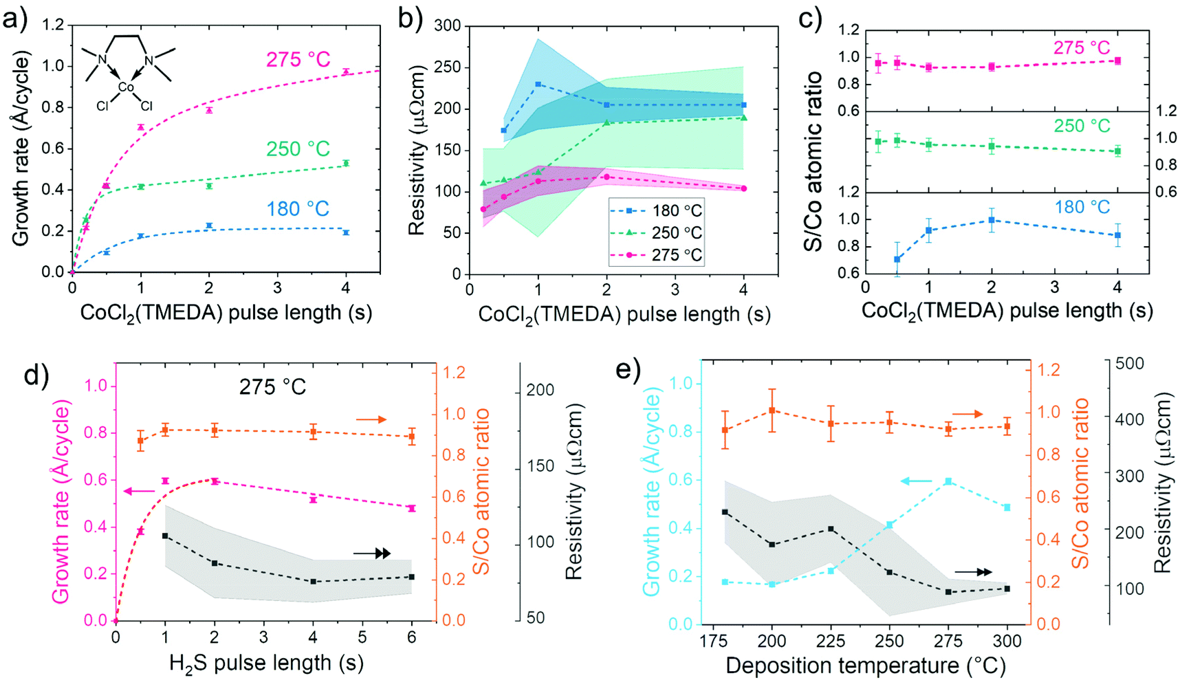 | ||
| Fig. 1 (a) Growth rate, (b) resistivity, and (c) S/Co atomic ratio versus CoCl2(TMEDA) pulse length at different deposition temperatures. Schematic structure of the CoCl2(TMEDA) precursor is shown as an inset in (a). Growth rate, resistivity and S/Co atomic ratio versus (d) H2S pulse length (at 275 °C) and (e) deposition temperature. Thicknesses and S/Co ratios were determined by EDS. The error bars in growth rates and S/Co ratios represent statistical measurement uncertainty (one standard deviation). The shaded areas around resistivity values represent film uniformity, i.e. variation (one standard deviation) in sheet resistance over the 5 × 5 cm2 silicon substrate (resistivities calculated using a single thickness value per sample). The dashed lines are meant to guide the eye. The films were deposited on silicon (native oxide) using, unless otherwise noted, 1000 cycles with 1.0 s CoCl2(TMEDA) and 2.0 s H2S pulses separated by 1.0 s N2 purges. | ||
Supported by observed changes in crystalline texture as a function of CoCl2(TMEDA) pulse length, we propose that the slow saturation at 275 °C may be due to different crystalline facets having different growth rates as well as kinetics (see section S3 in the ESI† for the full explanation). Despite the atypical saturation, conformal films were deposited on trench structures at 275 °C (ESI, Fig. S4†).
The film uniformity improved at 275 °C when long CoCl2(TMEDA) pulse lengths were used. The non-uniformity of sheet resistance over the 5 × 5 cm2 silicon substrate decreased from approximately 20% using ≤1 s pulses to less than 5% using 4 s CoCl2(TMEDA) pulses. At 180 °C, a similar trend with slightly higher non-uniformities was observed, whereas at 250 °C non-uniformity was high, 30–50%, regardless of the pulse lengths applied (Fig. 1b). In addition, the film resistivity was the lowest at 275 °C, namely 80–120 μΩ cm. The S/Co atomic ratio was measured to be 0.9–1.0 for the majority of the films (Fig. 1c) in agreement with the Co9S8 phase detected by XRD, which has a theoretical S/Co ratio of 0.89. The same Co9S8 phase has also been reported for the Co(iPrAMD)2 + H2S process.6,8,13,14,29 Deposition temperature of 275 °C was chosen for further experiments, unless otherwise noted, as it combined the highest growth rate with the best uniformity and lowest resistivity.
Varying the H2S pulse length at 275 °C showed that a growth rate of 0.6 Å per cycle was reached using 1.0 s H2S pulses, when the CoCl2(TMEDA) pulse was fixed to 1.0 s. The growth rate slightly decreased from 0.6 to 0.5 Å per cycle with an increase of the H2S pulse length from 1.0 to 6.0 s (Fig. 1d). The decrease in growth rate is postulated to be linked to changes in crystalline texture in the opposite direction compared to the changes observed as a function of CoCl2(TMEDA) pulse (section S3 in the ESI†). With increasing H2S pulse length, film resistivity decreased from approximately 100 to 80 μΩ cm. The S/Co ratio of the films remained unchanged within the measurement accuracy at approximately 0.9 when the H2S pulse length was varied.
One second N2 purges between the precursor pulses were found to be sufficient for removing excess precursor and reaction byproducts, thus preventing any gas phase reactions (ESI, Fig. S5†). Most of the films discussed later in this article were deposited using a pulse sequence optimized for throughput and film uniformity, namely 1.0 s CoCl2(TMEDA) and 2.0 s H2S pulses separated by 1.0 s N2 purges.
A more systematic look at the effect of deposition temperature confirmed the trends discussed above, i.e. an increase in growth rate, a decrease in resistivity, and an improvement in uniformity with an increase of temperature from 180 to 275 °C (Fig. 1e). At 300 °C, the growth rate started to decrease and decomposition of CoCl2(TMEDA) was visually observed as a dark film deposited in the quartz parts of the reactor in line with previous studies.32 However, good uniformity and low resistivity were still achieved at 300 °C. The growth rate of our process at 275 °C is higher compared to the previous Co(iPrAMD)2 + H2S process with reported growth rates of 0.27–0.4 Å per cycle at 80–165 °C depending on the reactor used.6,13,14,29
The resistivity of the films on silicon and soda lime glass substrates (80–220 μΩ cm depending on deposition conditions) was more than an order of magnitude lower compared to the ALD Co9S8 films grown using Co(iPrAMD)2 and H2S (3–5 mΩ cm).13 The bulk resistivity of metallic Co is 5.6 μΩ cm,44i.e. about an order of magnitude lower compared to our Co9S8 films. However, the resistivities of ALD Co films reported in the literature ranges from 10 to 200 μΩ cm.45 Thus, the low resistivity of our Co9S8 films is comparable to even some metallic cobalt ALD films.
Characterization of film crystallinity, morphology, and composition
The films deposited at all of the examined temperatures from 180 to 300 °C consisted of purely cubic Co9S8 (cobalt pentlandite) according to XRD (Fig. 2a; International Centre for Diffraction Data Powder Diffraction File (PDF) 86-2273). θ − 2θ XRD measurements revealed the films to exhibit preferred (111) orientation or texture (Fig. S10 in the ESI†).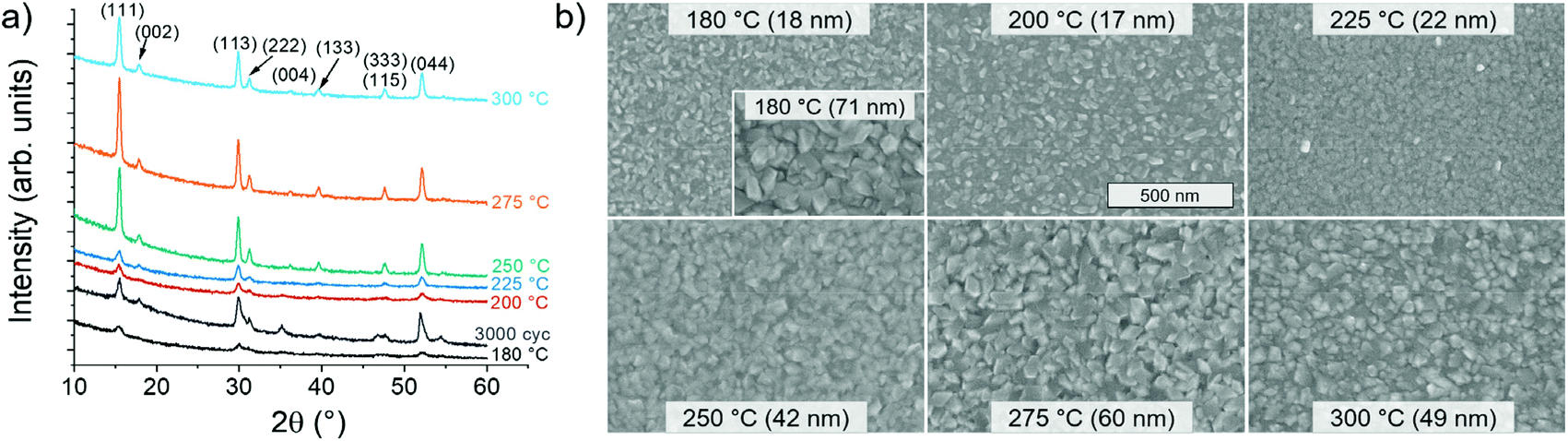 | ||
| Fig. 2 (a) Grazing incidence X-ray diffractograms (all Miller indices refer to Co9S8) and (b) SEM images of films deposited at different temperatures. The films were deposited on silicon (native oxide) using 1000 cycles except for the thicker film deposited at 180 °C using 3000 cycles that is shown in the inset. Film thicknesses determined by EDS are indicated in (b). | ||
Effect of deposition temperature on film crystallinity and texture was evaluated with the aid of a thicker film deposited at 180 °C using 3000 cycles. The broader and lower peaks observed in this film compared to the films of lower thickness deposited at 250 °C and above confirm that the film crystallinity improved and (111) texture strengthened with increasing deposition temperature.
All of the films appeared relatively rough in SEM (Fig. 2b). No major changes in the shape and size of the surface features as a function of deposition temperature were observed for films of similar thickness. The width of the grains ranged from about 50 to 100 nm for 50–70 nm thick films, while in thinner films the grains were smaller as expected.
Film composition was studied by time-of-flight elastic recoil detection analysis (ToF-ERDA), which confirmed the S/Co ratio of 0.9 for the films deposited at 250–300 °C, whereas it was 1.0 for the film deposited at 180 °C (Table 1). Detection of chlorine impurities in the films by ToF-ERDA was complicated by the similar atomic masses of sulfur and chlorine and the limited mass resolution of the setup. Thus, only upper limits of chlorine contents are reported. They suggest a higher chlorine content in the film deposited at 180 °C compared to the films grown at higher temperatures. Low oxygen, carbon, nitrogen, and hydrogen contents of less than 3 at% in total (∼4% at 300 °C) were observed in the bulk of the films. Oxygen likely originates from post-deposition oxidation, as supported by an increased concentration of oxygen observed on the film surface (ESI, Fig. S11†), whereas the other impurity elements likely come from the precursors used.
| Deposition temperature (°C) | Co (at%) | S (at%) | S/Co ratio | Cl (at%) | O (at%) | C (at%) | N (at%) | H (at%) |
|---|---|---|---|---|---|---|---|---|
| 180 | 47.0 ± 0.5 | 48.0 ± 0.5 | 1.02 ± 0.01 | <2.7 | 0.17 ± 0.01 | 0.80 ± 0.07 | 0.20 ± 0.04 | 1.24 ± 0.09 |
| 250 | 50.1 ± 0.9 | 45.6 ± 0.9 | 0.91 ± 0.01 | <1.2 | 0.68 ± 0.06 | 0.63 ± 0.09 | 0.19 ± 0.06 | 1.3 ± 0.2 |
| 275 | 49.4 ± 0.4 | 45.2 ± 0.4 | 0.92 ± 0.01 | <0.8 | 0.45 ± 0.04 | 0.63 ± 0.09 | 0.12 ± 0.04 | 1.2 ± 0.2 |
| 300 | 49.9 ± 0.9 | 45.4 ± 0.9 | 0.91 ± 0.01 | <0.8 | 0.66 ± 0.06 | 1.6 ± 0.2 | 0.29 ± 0.08 | 1.3 ± 0.2 |
Film nucleation and implications for area-selective deposition
In order to obtain more information on film nucleation, formation of continuous films, and possibilities for area-selective ALD, a series of thinner Co9S8 films was prepared on four substrates that were selected based on preliminary experiments. In terms of film thickness, the growth proceeded in a rather similar manner on silicon with either a native oxide (denoted native SiO2) or a thermal SiO2 layer (denoted thermal SiO2) as well as soda lime glass (denoted SLG) as shown in Fig. 3a. During the first 25 cycles, substrate-enhanced growth, in other words a higher growth rate of up to 3 Å per cycle was observed on these substrates, before the growth rate slowed down to the steady-state value of approximately 0.6 Å per cycle at 275 °C (ESI, Fig. S12†). In stark contrast, a clear nucleation delay was observed on HF-dipped hydrogen-terminated silicon (denoted Si–H), on which no growth was seen when 50 cycles or less were applied. | ||
| Fig. 3 (a) Thickness, (b) SEM images (thickness and resistivity values also indicated; thicknesses in italic measured by EDS, others by XRR; dl. = detection limit), (c) resistivity, and (d) root-mean-square roughness (Rq) of films deposited at 275 °C on different substrates versus number of ALD cycles. The dashed lines are meant to guide the eye. The error bars of EDS thicknesses represent statistical measurement uncertainty (one standard deviation). For XRR, the uncertainty was estimated to be smaller than the symbol size. The error bars in roughness represent variation within 3–5 AFM images recorded per sample (one standard deviation). | ||
Despite the similar growth rate evolution on native SiO2, thermal SiO2, and SLG, differences in morphology, continuity, and resistivity were observed. The films deposited on native SiO2 were electrically conductive already after 10 cycles, at a thickness of approximately 3.3 nm, although there may still be some holes in the film (Fig. 3b; information on additional samples in Fig. S13 and S14 in the ESI†). In contrast, the thinnest conductive film on SLG was 5.2 nm thick (25 cycles) and that on thermal SiO2 was 7.0 nm thick (50 cycles). The differences in the formation of a continuous film suggest more rapid nucleation and/or lower degree of agglomeration of the initially formed nuclei on native SiO2 compared to thermal SiO2 and SLG. Faster nucleation on native SiO2 would imply a higher number of reactive sites, which is plausible considering that the high temperatures used to prepare thermal SiO2 are known to decrease the density of reactive –OH groups.46 Differences in agglomeration, on the other hand, may be caused by a multitude of factors, both kinetic (e.g. diffusion rate) and thermodynamic (e.g. surface energy) in nature.
The resistivities of the ultrathin Co9S8 films were expectedly higher compared to the thicker films, up to a few hundred μΩ cm (Fig. 3c). The increased resistivity of the thinner films is likely due to increased electron scattering at the interfaces, as well as at grain boundaries.47 The resistivities of films of a given thickness on native SiO2 were somewhat lower compared to the other substrates (ESI, Fig. S15†). The native SiO2 substrates had sheet resistances of at least ten times higher than the thinnest Co9S8 films, so the substrate conductivity should not have a major effect on the measured values. The lower film resistivity on native SiO2 is thus likely linked to the faster formation of continuous films as discussed above. For the films deposited using at least 250 cycles (approximately 15 nm thick), the resistivities on the different substrates approached a stable value of less than 100 μΩ cm.
XRD peaks indicating formation of crystalline Co9S8 were observed after only 25 cycles on native SiO2 (ESI, Fig. S16a†). Thus, it seems likely that Co9S8 grows in crystalline form from the first cycles. No major changes in the preferred orientation with increasing film thickness were observed (ESI, Fig. S16b†). Qualitatively, the Co9S8 out-of-plane crystallite size on native SiO2 increased with increasing thickness as shown by decreasing XRD peak widths. At the same time, also the in-plane size of the surface features (grains) increased as observed by SEM (Fig. 3b).
On Si–H, a continuous film with a high resistivity of more than 600 μΩ cm was obtained only after 250 ALD cycles. The nucleation delay on Si–H was confirmed by AFM, which showed practically no change in roughness up to 50 cycles, in contrast to a monotonous increase of film roughness on native and thermal SiO2 (Fig. 3d, images in Fig. S17 in the ESI†). For thicker films, the roughnesses on native SiO2, thermal SiO2, and Si–H were similar and relatively large (4–5 and 6–8 nm using 500 and 1000 cycles). The resistivity and non-uniformity of the films on Si–H remained higher compared to the SiO2 substrates.
These results indicate that the present ALD process enables inherent area-selective deposition of Co9S8 on oxide-covered silicon with readily prepared Si–H as a non-growth surface. The 50 cycle nucleation delay on Si–H means that conductive and continuous, 6–7 nm thick films can be deposited on SiO2 before any growth is detected on Si–H. Because of the high conductivity of Co9S8, the system may be described as selective growth of a metal (Co9S8) on a dielectric (SiO2) with a semiconductor (Si–H) as the non-growth area. Metal-on-dielectric systems are more uncommon in the area-selective ALD literature compared to the selective dielectric-on-dielectric deposition.48 Besides, there are very few reports on area-selective deposition of metal sulfides. Therefore, the process should be a valuable addition to the area-selective deposition toolbox.
Film growth on different substrates: toward epitaxial growth
In addition to the substrates described above, Co9S8 films were successfully grown on a variety of other dielectric, semiconducting, and metallic substrates, including sapphire (α-Al2O3), mica, GaN, and different ALD-grown films (Al2O3, Ir, and TiO2). The morphologies of 1000 cycle films were similar on most of the substrates, although on sapphire and ALD-TiO2 the size of the surface features was somewhat smaller and on ALD-Ir larger compared to the other substrates, i.e. native SiO2, thermal SiO2, Si–H, SLG, and ALD-Al2O3 (Fig. 4). | ||
| Fig. 4 SEM images of films deposited on different substrates at 275 °C using 1000 cycles. | ||
XRD revealed differences in the crystalline texture: the films on ALD-Al2O3 were more strongly (111) oriented compared to sapphire and native SiO2 and even more so compared to Si–H, SLG, and thermal SiO2 (ESI, Fig. S18†). On ALD-Ir and ALD-TiO2, the films appeared (113) textured, which may also be affected by the rougher morphology of these substrates.
Some differences in growth rate and resistivity between the different substrates studied were also observed (ESI, Fig. S19†). These maybe be due to differences in nucleation delay and the effect of crystallographic texture on growth rate (section S3 in the ESI†).
On single-crystalline mica and GaN substrates, a very different surface morphology mostly exposing triangular grains was observed. XRD showed the films to be very strongly (111) textured to a degree where no Co9S8 peaks were observed in the GIXRD measurements, and only strong (111), (222), and (333) reflections were observed in the θ − 2θ measurements. AFM confirmed the different morphology and larger size of the surface features on GaN and mica compared to Si (ESI, Fig. S20†).
The very strong (111) texture on mica and GaN may suggest an epitaxial alignment between Co9S8 and these single-crystalline substrates. First, it was confirmed that the out-of-plane peaks attributed to Co9S8 did not originate from the multilayered GaN substrate comprised of graded Al(Ga)N buffer layers on Si(111) (ESI, Fig. S21a and b†). Then, the texture was quantified using a rocking curve (ω scan) measurement, which confirmed the strong (111) texture with a relatively small full-width at half-maximum (FWHM) of 1.5° (ESI, Fig. S21c†).
An in-plane pole figure measurement of the (111)Co9S8 reflection revealed a sharp pole in the middle, corresponding to the (111) out-of-plane orientation (Fig. 5a; extracted cut along 90°β in Fig. S22a in the ESI†). In addition, six poles tilted by 70.5° with respect to the substrate plane (i.e. at 19.5°α) were observed (see also Fig. S22b in the ESI†), which were attributed to the {![[1 with combining macron]](https://www.rsc.org/images/entities/char_0031_0304.gif) 11} planes that are at an angle of 70.5° with respect to the (111) plane in the crystal structure of Co9S8 (cubic, space group 225, Fm
11} planes that are at an angle of 70.5° with respect to the (111) plane in the crystal structure of Co9S8 (cubic, space group 225, Fm![[3 with combining macron]](https://www.rsc.org/images/entities/char_0033_0304.gif) m). The observation of six poles rather than a continuous ring confirms the epitaxial nature of the films and, as the (11) reflection has only three-fold rotational symmetry which would result in three peaks every 120°, suggests a presence of two domains rotated by 60° with respect to each other.
m). The observation of six poles rather than a continuous ring confirms the epitaxial nature of the films and, as the (11) reflection has only three-fold rotational symmetry which would result in three peaks every 120°, suggests a presence of two domains rotated by 60° with respect to each other.
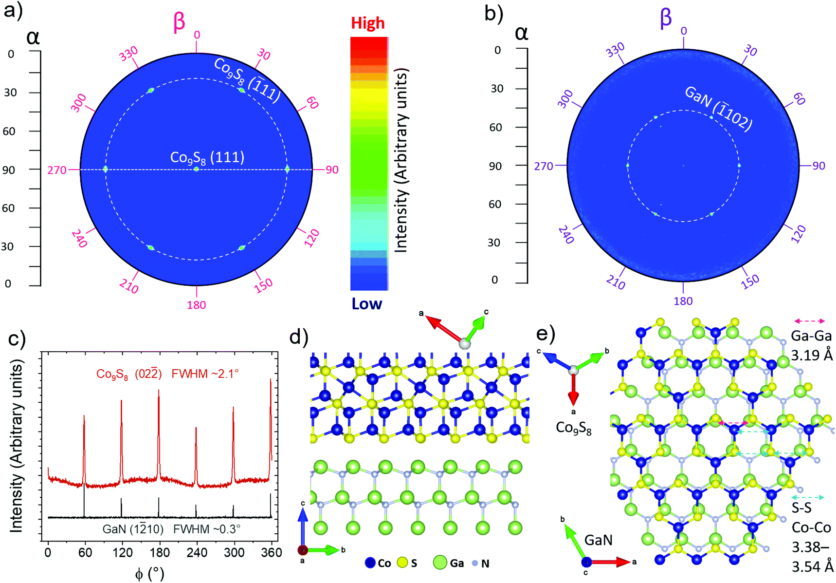 | ||
Fig. 5 In-plane pole figures at (a) 15.5°2θ showing the out-of-plane (111)Co9S8 reflection in the middle (90°α) and (11) reflections tilted by 70.5° (19.5°α) and (b) 48.27°2θ showing the (102)GaN reflections at 47°α. Both pole figures were measured with the sample in the same orientation. (c) In-plane φ scans of (02![[2 with combining macron]](https://www.rsc.org/images/entities/char_0032_0304.gif) )Co9S8 (25.35°2θχ) and (110)GaN (57.95°2θχ) reflections. The data has been vertically offset for clarity. Schematic of a possible epitaxial arrangement (111)[01]Co9S8||(0001)[20]GaN: (d) cross-sectional and (e) top view. In top view, only one puckered Co–S “layer” is shown for clarity. Selected atomic distances are indicated. )Co9S8 (25.35°2θχ) and (110)GaN (57.95°2θχ) reflections. The data has been vertically offset for clarity. Schematic of a possible epitaxial arrangement (111)[01]Co9S8||(0001)[20]GaN: (d) cross-sectional and (e) top view. In top view, only one puckered Co–S “layer” is shown for clarity. Selected atomic distances are indicated. | ||
A second pole figure of the substrate (102)GaN reflection (Fig. 5b and Fig. S22c in the ESI†) revealed six sharp poles tilted by 43° with respect to the substrate (47°α) surface that were observed at the same β (sample rotation around its normal) angles as the (11)Co9S8 poles. Six poles are expected due to the six-fold rotational symmetry of wurtzite GaN (hexagonal, space group 186, P63mc, PDF 2-1078). The three sharp and weak poles observed at 35°α and six poles at 62°α were attributed to the substrate as confirmed by a measurement of a bare substrate but they could not be assigned to any known reflection. These extra poles may be due to multiple scattering effects or the non-monochromatic radiation used.
The epitaxial film-substrate registration was confirmed by in-plane measurements, which detect planes perpendicular to the substrate surface. In the in-plane φ scans (full 360° rotation), six peaks from both (02)Co9S8 and (110)GaN reflections were observed at the same φ angles (Fig. 5c). Both of these reflections have six-fold rotational symmetry, although any of the possible surfaces have, at most, three-fold symmetry. Whether one or two Co9S8 domains are present thus cannot be determined from this measurement. The presence of two domains was shown by the in-plane pole figure measurements discussed earlier, which is also in line with the observation of some approximately triangular grains rotated by 60° or 180° with respect to each other by SEM (Fig. 4). The in-plane pole figure and in-plane φ scan measurements therefore suggest epitaxial film-substrate relations (111)[01]Co9S8||(0001)[20]GaN and (111)[10]Co9S8||(0001)[20]GaN, the two orientations being related by a 60° rotation.
The 2.1° FWHM of the (02)Co9S8 in-plane peaks is reasonably small, although clearly larger than that of the (110)GaN reflection (0.3°), suggesting good epitaxial quality considering the low deposition temperature. Thinner films deposited on GaN using 100 and 250 cycles were also found to be epitaxial with similar in- and out-of-plane disorder to the 1000 cycle film (ESI, Fig. S23†). Furthermore, the 100 cycle film on GaN was already conductive at a thickness of approximately 5 nm. All of the epitaxial Co9S8/GaN films were relatively rough with roughnesses similar to the polycrystalline Co9S8 films deposited on silicon.
A look at the atomic structures of GaN and Co9S8 in the observed alignment shows obvious similarities that may explain the epitaxial growth between two materials which at the first sight have very different structures (a possible interface drawn in Fig. 5d, e and discussion in section S8 in the ESI†). An approximately 10% mismatch between the illustrated surfaces suggests that instead of conventional epitaxy, a domain matching epitaxy mechanism49 may be in play (section S8 in the ESI†).
Of the other single-crystalline substrates evaluated, on mica epitaxial growth with several distinct domains and large in-plane disorder was observed, as discussed in the ESI (section S9).† Large disorder and multiple domains are rather common for van der Waals epitaxy, for which the film-substrate bonding is weak,50,51 suggesting that the Co9S8/mica system may follow this mechanism. On sapphire, on the other hand, even the out-of-plane (111) texture of the Co9S8 films was not very strong, which rules out epitaxial alignment (section S10 in the ESI†).
We hope that the demonstration of the first epitaxial Co9S8 films inspires further studies on the epitaxial Co9S8/GaN system including film structure, substrate/film interface, and film properties. We believe that careful analysis of the system may both improve fundamental understanding of epitaxy of dissimilar materials as well as enable preparation of higher quality Co9S8 films with improved properties.
High-temperature stability in different atmospheres
High-temperature XRD (HTXRD) was used to evaluate the stability and reactivity of the Co9S8 films under different atmospheres. On one hand, high-temperature stability is required for various applications and device processing steps. On the other hand, post-deposition annealing can also be used to tune the composition of the films. Fig. 6 shows a summary of the phase transformations observed under inert, reducing, and oxidizing atmospheres as will be discussed below.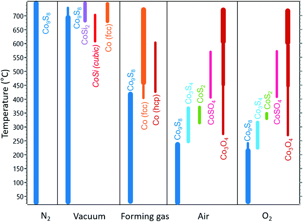 | ||
| Fig. 6 Summary of crystalline phases observed during in situ high-temperature GIXRD measurements performed under different atmospheres. The widths of the lines referring to the different phases represent an estimation on the relative amounts of the different phases based on peak intensities. | ||
Under a flowing, reduced pressure (30 mbar) N2 atmosphere, no changes in the crystallinity and phase composition were observed upon heating up to the highest evaluated temperature of 750 °C (ESI, Fig. S27†). The resistivity of the film decreased from 95 to 65 μΩ cm and although minor changes in film morphology were observed, the film remained continuous after the annealing (ESI, Fig. S28†). In the published Co–S phase diagram, Co9S8 has been indicated to be stable up to 830 °C.3 The high stability, lack of reactions with silicon, and absence of strong agglomeration at these temperatures is encouraging considering possible use of Co9S8 in applications where conductive films are needed and high-temperature processing is encountered.
Under a dynamic vacuum (approximately 10−5 mbar), the Co9S8 film was stable up to 600 °C, where cubic CoSi (PDF 8-362) appeared to form (ESI, Fig. S29†). At 675 °C, fcc Co (PDF 15-806) and cubic CoSi2 (PDF 38-1449) were also observed to form. After heating to 750 °C and cooling to room temperature, only fcc Co and CoSi2 were observed (ESI, Fig. S30†). The formation of CoSix is likely preceded by loss of sulfur driven by the low pressure conditions and formation of either a sulfur-poor CoSx phase or metallic Co, which can then diffuse through the native SiO2 layer to react with the silicon substrate. Indeed, CoSi2 has been reported to form by a reaction of Co thin film with silicon at 700 °C.52,53
Under a reducing forming gas environment (10% H2/90% N2, atmospheric pressure), the Co9S8 films were stable up to approximately 400 °C, whereupon metallic cobalt started to form (Fig. 7). The film was completely transformed to cobalt at 475 °C, mainly in the fcc phase (PDF 15-806), with a minor contribution from hcp Co (PDF 5-727). Metallic Co remained until the end of the measurement at 725 °C. After cooling down to room temperature, the film consisted of mostly fcc Co with some hcp Co present (ESI, Fig. S31a†). In bulk, hcp Co is known as the low-temperature phase, which ideally transforms to the high-temperature fcc phase at 422 °C.3 The formed metallic film was discontinuous (ESI, Fig. S31b†), as is often observed after high-temperature reduction of compound films to metals.32 Interestingly, formation of CoSix was not observed, unlike in the measurement in vacuum. Notably, the temperature needed for reduction of Co9S8 was considerably higher compared to the reduction of CoO films grown from the same cobalt precursor (250 °C in the same atmosphere),32 which reflects the high stability of Co9S8.
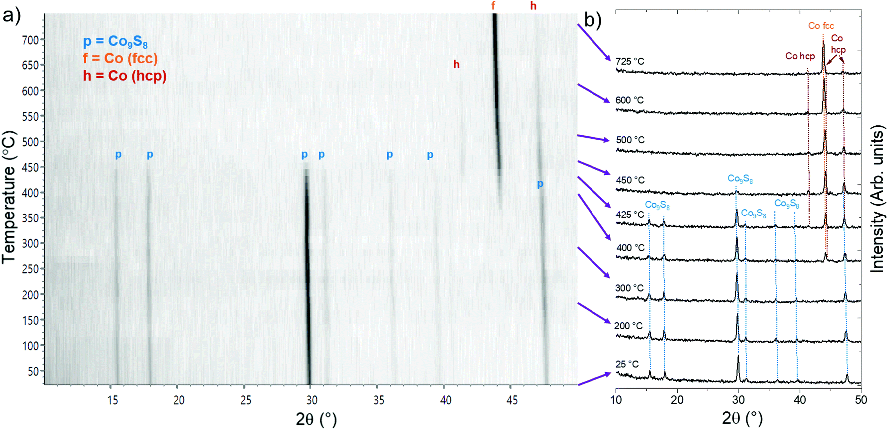 | ||
| Fig. 7 (a) High-temperature grazing incidence X-ray diffractograms during heating in a forming gas atmosphere (10% H2/90% N2, atmospheric pressure) from 25 to 725 °C (measured at 25 °C intervals), where light and dark represent low and high intensities, respectively. (b) Selected diffractograms measured at different temperatures. Peaks attributed to different phases were identified by symbols and lines of different colors. The studied film was deposited on silicon (native oxide) at 275 °C using 1000 cycles. | ||
Finally, the stability of Co9S8 films under oxidizing conditions was evaluated by annealing in air (Fig. 8). No changes were observed up to 225 °C, whereupon Co9S8 started to convert to Co3S4 (linnaeite, PDF 42-1448). Formation of Co3O4 (PDF 42-1467) was observed at 275 °C, and the oxide coexisted with various sulfide and sulfate phases during the measurement: with Co3S4 up to 300 °C, with Co3S4 and CoS2 (cattierite, PDF 41-1471) at 325–375 °C, and with CoSO4 (PDF 46-4) at 400–550 °C until Co3O4 was the only phase present at 575 to 725 °C.
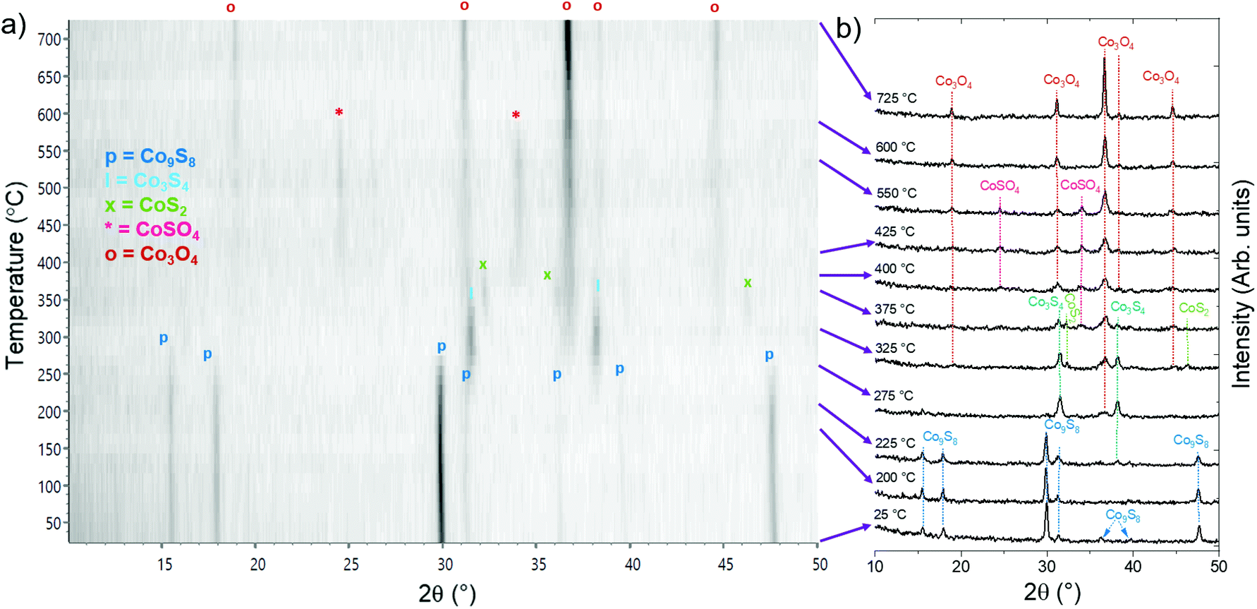 | ||
| Fig. 8 (a) High-temperature grazing incidence X-ray diffractograms during heating in air (atmospheric pressure) from 25 to 725 °C (measured at 25 °C intervals), where light and dark represent low and high intensities, respectively. (b) Selected diffractograms measured at different temperatures. Peaks attributed to different phases were identified by symbols and lines of different colors. The studied film was deposited on silicon (native oxide) at 275 °C using 1000 cycles. | ||
One potential explanation for the formation of phases with a higher sulfur content compared to Co9S8, i.e. Co3S4 and CoS2, may be release of elemental sulfur upon gradual oxidation of Co9S8 to Co3O4. While sulfur will eventually oxidize to SOx under oxidizing conditions, we hypothesize that at low enough temperatures, part of the elemental sulfur can survive long enough to form more sulfur-rich CoSx phases by reacting with Co9S8. At higher temperatures in oxygen-rich atmosphere, these sulfide phases may be further oxidized to CoSO4, while the excess sulfur can be released as gaseous SOx. Similarly, decomposition of CoSO4 to Co3O4 may release the sulfur as SOx species.
After cooling down to room temperature, a rough but continuous Co3O4 film was obtained (ESI, Fig. S32†). The observed oxidation and phase transition temperatures are similar to a previous study on Co3S4 thin films made by chemical bath deposition.54
Under an atmospheric pressure of pure oxygen, the high-temperature reactions were similar to those in laboratory air, although some of the phase transitions occurred at slightly lower temperatures (ESI, Fig. S33†) and the resulting oxide film appeared to be more strongly crystallized (ESI, Fig. S34†).
Conclusions
In this work, we have developed a new ALD process for Co9S8 thin films using CoCl2(TMEDA) with H2S. Compared to the earlier CoSx ALD processes, the precursor CoCl2(TMEDA) is more easily synthesized using inexpensive starting materials, and the resulting Co9S8 films have a considerably lower resistivity. Using our new process, highly conductive, pure, and crystalline Co9S8 films can be deposited between 180 and 300 °C. The lowest resistivity (80 μΩ cm), best uniformity, and highest growth rate are achieved at 275 °C. Electrically conductive films as thin as approximately 3 nm thick can be prepared on silicon with a native oxide layer. Area-selective deposition is enabled by fast nucleation on oxide-covered silicon in contrast to at least 50 cycle nucleation delay on Si–H, enabling deposition of continuous, at least 5 nm thick films without any growth on Si–H. Besides silicon oxide, Co9S8 films can also be deposited on different oxide, metal, and nitride substrates. The first ever epitaxial Co9S8 films were obtained on GaN, as studied in detail by XRD. The Co9S8 films are stable up to at least 750 °C in N2, 600 °C in high vacuum, 400 °C in forming gas, and 225 °C in air or pure O2. The high stability is promising for use in applications requiring high-temperature processing steps. Overall, we believe the presented process may be interesting for, for example, metal barrier, liner, and seed layers for interconnects as well as various energy technology applications due to the high conductivity of the films and scalable, simple, low cost synthesis of the cobalt precursor.Conflicts of interest
There are no conflicts to declare.Acknowledgements
The research was supported by ASM Microchemistry. Imec is thanked for supplying the epitaxial GaN substrates.Notes and references
- C. N. R. Rao and K. P. R. Pisharody, Prog. Solid State Chem., 1976, 10, 207 CrossRef.
- Y. O. Chen and Y. A. Chang, Metall. Trans. B, 1978, 9, 61 CrossRef.
- H. Rau, J. Phys. Chem. Solids, 1976, 37, 931 CrossRef CAS.
- D. Xiong, Q. Zhang, S. M. Thalluri, J. Xu, W. Li, X. Fu and L. Liu, Chem. – Eur. J., 2017, 23, 8749 CrossRef CAS PubMed.
- X. Ma, W. Zhang, Y. Deng, C. Zhong, W. Hu and X. Han, Nanoscale, 2018, 10, 4816 RSC.
- H. Li, Z. Guo and X. Wang, J. Mater. Chem. A, 2017, 5, 21353 RSC.
- L.-L. Feng, M. Fan, Y. Wu, Y. Liu, G.-D. Li, H. Chen, W. Chen, D. Wang and X. Zou, J. Mater. Chem. A, 2016, 4, 6860 RSC.
- D. Kim, J.-G. Song, H. Yang, H. Lee, J. Park and H. Kim, Nanoscale, 2019, 11, 844 RSC.
- Y. Chen, J.-M. Tarascon and C. Guéry, Electrochim. Acta, 2013, 99, 46 CrossRef CAS.
- L. Zheng, X. Sun, L. Chen, C. Bao, W. Luo, N. Huang, P. Sun, Y. Sun, L. Fang and L. Wang, J. Mater. Sci., 2016, 51, 4150 CrossRef CAS.
- S.-H. Chang, M.-D. Lu, Y.-L. Tung and H.-Y. Tuan, ACS Nano, 2013, 7, 9443 CrossRef CAS PubMed.
- S. Y. Chae, Y. J. Hwang, J.-H. Choi and O.-S. Joo, Electrochim. Acta, 2013, 114, 745 CrossRef CAS.
- H. Li, Y. Gao, Y. Shao, Y. Su and X. Wang, Nano Lett., 2015, 15, 6689 CrossRef CAS PubMed.
- W. Xiong, K. Hu, Z. Li, Y. Jiang, Z. Li, Z. Li and X. Wang, Nano Energy, 2019, 66, 104149 CrossRef CAS.
- C. Auth, et al., in 2017 IEEE International Electron Devices Meeting (IEDM), 2017, p. 673 Search PubMed.
- X. F. Qian, X. M. Zhang, C. Wang, Y. Xie and Y. T. Qian, Inorg. Chem., 1999, 38, 2621 CrossRef CAS.
- N. Kumar, N. Raman and A. Sundaresan, Z. Anorg. Allg. Chem., 2014, 640, 1069 CrossRef CAS.
- Y. N. Ko, S. H. Choi, S. B. Park and Y. C. Kang, Chem. – Asian J., 2014, 9, 572 CrossRef CAS PubMed.
- K. Ramasamy, W. Maneeprakorn, N. Iqbal, M. A. Malik and P. O'Brien, Int. J. Nanosci., 2011, 10, 815 CrossRef CAS.
- V. G. Bessergenev, R. J. F. Pereira and A. M. Botelho do Rego, Surf. Coat. Technol., 2007, 201, 9141 CrossRef CAS.
- R. Nomura and N. Nakai, Trans. Mater. Res. Soc. Jpn., 2003, 28, 1287 Search PubMed.
- S. M. George, Chem. Rev., 2010, 110, 111 CrossRef CAS PubMed.
- R. W. Johnson, A. Hultqvist and S. F. Bent, Mater. Today, 2014, 17, 236 CrossRef CAS.
- M. Ritala and J. Niinistö, in Chemical Vapor Deposition: Precursors, Processes and Applications, ed. A. C. Jones and M. L. Hitchman, Royal Society of Chemistry, Cambridge, 2009, pp. 158–206 Search PubMed.
- M. Ritala and J. Niinistö, ECS Trans., 2009, 25(8), 641 CrossRef CAS.
- I. J. Raaijmakers, ECS Trans., 2011, 41(2), 3 CrossRef CAS.
- Atomic Limits ALD Database, https://www.atomiclimits.com/alddatabase/(accessed August 2021).
- N. P. Dasgupta, X. Meng, J. W. Elam and A. B. F. Martinson, Acc. Chem. Res., 2015, 48, 341 CrossRef CAS PubMed.
- A. W. Peters, Z. Li, O. K. Farha and J. T. Hupp, ACS Nano, 2015, 9, 8484 CrossRef CAS PubMed.
- Z. Guo and X. Wang, Angew. Chem., Int. Ed., 2018, 57, 5898 CrossRef CAS PubMed.
- Strem Chemicals, Inc., Product Catalog: Bis(N,N′-di-i-propylacetamidinato)cobalt(II), https://www.strem.com/catalog/v/27-0486/16/cobalt_635680-58-9 (accessed June 2021).
- K. Väyrynen, T. Hatanpää, M. Mattinen, M. Heikkilä, K. Mizohata, K. Meinander, M. Ritala and M. Leskelä, Chem. Mater., 2018, 30, 3499 CrossRef.
- K. Väyrynen, T. Hatanpää, M. Mattinen, K. Mizohata, K. Meinander, J. Räisänen, J. Link, R. Stern, M. Ritala and M. Leskelä, Adv. Mater. Interfaces, 2018, 6, 1801291 CrossRef.
- H.-E. Nieminen, M. Kaipio and M. Ritala, Chem. Mater., 2020, 32, 8120 CrossRef CAS.
- T. Suntola, Thin Solid Films, 1992, 216, 84 CrossRef CAS.
- N. P. Dasgupta, J. F. Mack, M. C. Langston, A. Bousetta and F. B. Prinz, Rev. Sci. Instrum., 2010, 81, 044102 CrossRef PubMed.
- W. de Poel, S. Pintea, J. Drnec, F. Carla, R. Felici, P. Mulder, J. A. A. W. Elemans, W. J. P. van Enckevort, A. E. Rowan and E. Vlieg, Surf. Sci., 2014, 619, 19 CrossRef CAS.
- P. R. Ribic and G. Bratina, Surf. Sci., 2007, 601, 44 CrossRef CAS.
- R. A. Waldo, in Microbeam Analysis, ed. D. E. Newbury, San Francisco Press, San Francisco, 1988, pp. 310–314 Search PubMed.
- Co9S8 Crystal Structure, SpringerMaterials (online database), ed. P. Villars and K. Cenzual, Springer, Heidelberg, 2016, https://materials.springer.com/isp/crystallographic/docs/sd_0375057 (accessed June 2021) Search PubMed.
- K. Nagao and E. Kagami, Rigaku J., 2011, 27, 6 CAS.
- S. Kobayashi, Rigaku J., 2010, 26, 3 CAS.
- K. Momma and F. Izumi, J. Appl. Crystallogr., 2011, 44, 1272 CrossRef CAS.
- CRC Handbook of Chemistry and Physics, ed. J. R. Rumble, CRC Press, Boca Raton, FL, 102nd edn, 2021, http://www.hbcpnetbase.com/ (accessed June 2021) Search PubMed.
- K. Väyrynen, PhD thesis, University of Helsinki, 2019. Available at https://helda.helsinki.fi/handle/10138/305438.
- L. T. Zhuravlev, Langmuir, 1987, 3, 316 CrossRef CAS.
- R. B. Milligan and D. Li, ECS Trans., 2010, 33(2), 159 CrossRef CAS.
- G. N. Parsons and R. D. Clark, Chem. Mater., 2020, 32, 4920 CrossRef CAS.
- J. Narayan and B. C. Larson, J. Appl. Phys., 2003, 93, 278 CrossRef CAS.
- M. Mattinen, P. J. King, G. Popov, J. Hämäläinen, M. J. Heikkilä, M. Leskelä and M. Ritala, 2D Mater., 2020, 7, 011003 CrossRef CAS.
- M. Nakano, Y. Wang, Y. Kashiwabara, H. Matsuoka and Y. Iwasa, Nano Lett., 2017, 17, 5595 CrossRef CAS PubMed.
- J.-H. Yoon, H.-B.-R. Lee, G.-H. Gu, C.-G. Park and H. Kim, Korean J. Mater. Res., 2012, 22, 202 CrossRef CAS.
- C. T. Joensson, I. A. Maximov, H. J. Whitlow, V. Shutthanandan, L. Saraf, D. E. McCready, B. W. Arey, Y. Zhang and S. Thevuthasan, Nucl. Instrum. Methods Phys. Res., Sect. B, 2006, 249, 532 CrossRef CAS.
- F. C. Eze, Semicond. Sci. Technol., 2001, 16, 362–366 CrossRef CAS.
Footnotes |
| † Electronic supplementary information (ESI) available: Results of additional deposition experiments and film characterization, further details and discussion of epitaxial growth, XRD measurements on film stability in different atmospheres. See DOI: 10.1039/d1dt02315b |
| ‡ Present address: Department of Applied Physics, Eindhoven University of Technology, P.O. Box 513, 5600 MB Eindhoven, The Netherlands. |
| This journal is © The Royal Society of Chemistry 2021 |