
 Open Access Article
 This Open Access Article is licensed under a Creative Commons Attribution-Non Commercial 3.0 Unported Licence
Solution-processed two-dimensional materials for next-generation photovoltaics
Sebastiano
Bellani
 ab,
Antonino
Bartolotta
c,
Antonio
Agresti
d,
Giuseppe
Calogero
c,
Giulia
Grancini
e,
Aldo
Di Carlo
df,
Emmanuel
Kymakis
g and
Francesco
Bonaccorso
*ab
ab,
Antonino
Bartolotta
c,
Antonio
Agresti
d,
Giuseppe
Calogero
c,
Giulia
Grancini
e,
Aldo
Di Carlo
df,
Emmanuel
Kymakis
g and
Francesco
Bonaccorso
*ab
aBeDimensional S.p.A., Via Lungotorrente Secca 30R, 16163 Genova, Italy. E-mail: f.bonaccorso@bedimensional.it
bIstituto Italiano di Tecnologia, Graphene Labs, via Moreogo 30, 16163 Genova, Italy
cCNR-IPCF, Istituto per i Processi Chimico-Fisici, Via F. Stagno D’alcontres 37, 98158 Messina, Italy
dCHOSE – Centre for Hybrid and Organic Solar Energy, University of Rome “Tor Vergata”, via del Politecnico 1, 00133 Roma, Italy
eUniversity of Pavia and INSTM, Via Taramelli 16, 27100 Pavia, Italy
fL.A.S.E. – Laboratory for Advanced Solar Energy, National University of Science and Technology “MISiS”, 119049 Leninskiy Prosect 6, Moscow, Russia
gDepartment of Electrical & Computer Engineering, Hellenic Mediterranean University, Estavromenos 71410 Heraklion, Crete, Greece
First published on 8th September 2021
Abstract
In the ever-increasing energy demand scenario, the development of novel photovoltaic (PV) technologies is considered to be one of the key solutions to fulfil the energy request. In this context, graphene and related two-dimensional (2D) materials (GRMs), including nonlayered 2D materials and 2D perovskites, as well as their hybrid systems, are emerging as promising candidates to drive innovation in PV technologies. The mechanical, thermal, and optoelectronic properties of GRMs can be exploited in different active components of solar cells to design next-generation devices. These components include front (transparent) and back conductive electrodes, charge transporting layers, and interconnecting/recombination layers, as well as photoactive layers. The production and processing of GRMs in the liquid phase, coupled with the ability to “on-demand” tune their optoelectronic properties exploiting wet-chemical functionalization, enable their effective integration in advanced PV devices through scalable, reliable, and inexpensive printing/coating processes. Herein, we review the progresses in the use of solution-processed 2D materials in organic solar cells, dye-sensitized solar cells, perovskite solar cells, quantum dot solar cells, and organic–inorganic hybrid solar cells, as well as in tandem systems. We first provide a brief introduction on the properties of 2D materials and their production methods by solution-processing routes. Then, we discuss the functionality of 2D materials for electrodes, photoactive layer components/additives, charge transporting layers, and interconnecting layers through figures of merit, which allow the performance of solar cells to be determined and compared with the state-of-the-art values. We finally outline the roadmap for the further exploitation of solution-processed 2D materials to boost the performance of PV devices.
 Sebastiano Bellani | Sebastiano Bellani is a researcher at BeDimensional S.p.A. He received his PhD from Politecnico di Milano, while working at the Istituto Italiano di Tecnologia. Here, he investigated solid/liquid interfaces in organic semiconductor water-gated organic field-effect transistors, hybrid organic–inorganic photoelectrochemical cells, and biopolymer-based devices for optical cellular stimulation. Currently, he is participating at the European Commission's Future and Emerging Technology Graphene Flagship. He has been the deputy leader of Graphene Flagship's Solar Farm Spearhead Project. His studies are focused on chemical–physical, spectroscopic, and photoelectrochemical characterizations of solution-processed two-dimensional materials and their energy-related applications including photovoltaics, (photo)electrocatalysis, and energy storage systems. |
 Antonino Bartolotta | Antonino Bartolotta is a researcher at the Institute for the Chemical Physical Processes of the Italian National Research Council (CNR-IPCF). He gained his degree in chemistry from the University of Messina in Italy. His scientific activity started in the field of condensed matter physics, mainly devoted to glass transition and dynamical processes in disordered systems (glasses, polymers, and vitreous ionic conductors). Currently, his research is focused in the field of nanomaterials and energy conversion and storage devices. He has been involved in several research projects, and he is the author/co-author of many publications in international peer-reviewed journals and book chapters. |
 Antonio Agresti | Antonio Agresti is an Assistant Professor at the Department of Electronic Engineering at the University of Rome Tor Vergata since 2016. His research activity mainly involves the design, engineering, fabrication, and electrical/spectroscopic characterization of hybrid and organic solar cells; use of graphene and transition metal dichalcogenides and emerging two-dimensional materials such as MXenes for perovskite solar cells, tandem devices, large-area modules, and panels. He has authored/co-authored more than 50 publications and has participated as an invited speaker to several conferences in the renewable energy field. He is currently the deputy leader of Horizon 2020 Spearhead 5—Graphene Core 3 project. |
 Giuseppe Calogero | Giuseppe Calogero is a researcher at the Institute for the Chemical Physical Processes of the Italian National Research Council (CNR-IPCF), Messina, and he works in the field of energy and electron transfer processes. His research activity has mainly focused on the manufacturing, study, and characterization of dye-sensitized solar cells (DSSCs). He has synthetized supramolecular complexes based on polypyridine metal complexes and developed new nanostructured materials for DSSC applications, with focus on design, preparation, and processing. He has authored over 60 articles in peer-reviewed international journals. |
 Giulia Grancini | Giulia Grancini is an Associate Professor in Chemistry at the University of Pavia, leading the PVsquared2 team and the ERC Project “HYNANO” aiming at the development of advanced hybrid perovskites solar cells. She obtained her PhD in Physics from Politecnico di Milano in 2012 and worked as a Post-Doc Researcher at IIT, Milano. From 2015 to 2019, she joined the École Polytechnique Fédérale de Lausanne awarded by SNSF with the Ambizione Energy Grant. In 2020, she won the Journal of Materials Chemistry Lectureship. She is currently the USERN Ambassador for Italy and a board member of the Young Academy of Europe. In 2019 and 2020, she appeared among highly cited scientists. In 2020, she was listed in “100 Experts,” which identified the top Italian women scientists in STEM. She is the author of 94 publications and owns 2 patents. |
 Aldo Di Carlo | Aldo Di Carlo is a Full Professor at the University of Rome Tor Vergata and Director of the Institute of Structure of Matter of the National Research Council. His research activity mainly involves the design, fabrication, and characterization of solution-processed solar cells and other optoelectronic devices. He was the founder of the Centre for Hybrid and Organic Solar Energy (CHOSE), which involved more than 35 researchers. He was the CTO of Dyepower, a consortium for the industrialization of dye solar cells for façade applications. He has authored/co-authored more than 400 publications, review articles, and book chapters, and he owns 13 patents. |
 Emmanuel Kymakis | Emmanuel Kymakis is a Full Professor at the Department of Electrical and Computer Engineering at the Hellenic Mediterranean University (HMU) and Vice President of the HMU Research Center. He obtained his PhD in engineering from the University of Cambridge in 2003. His research focuses on graphene and related 2D materials with regard to the interfacial engineering of emerging solar cells for improved performance and stability, as well as on the performance evaluation of PV systems. He was named as a ChemComm Emerging Investigator and served as a member of the founding GA of HFRI. He is the leader of the Energy Generation WP of the FET Flagship Initiative, Graphene Flagship. |
 Francesco Bonaccorso | Francesco Bonaccorso is the Founder and Scientific Director of BeDimensional S.p.A. and Visiting Scientist at the Istituto Italiano di Tecnologia. He gained his PhD from the University of Messina after working at the Italian National Research Council, the University of Cambridge, and the University of Vanderbilt. In 2009, he was awarded a Royal Society Newton International Fellowship at Cambridge University, and a Fellowship at Hughes Hall, Cambridge, receiving his MA. He was responsible in defining the ten years scientific and technological roadmap for the Graphene Flagship. He is now the deputy of the Innovation of Flagship. He was featured as 2016 Emerging Investigator by Journal of Materials Chemistry A and in 2019, by ChemPlusChem. His research interests encompass both fundamental understanding and solution processing of novel nanomaterials and their technological applications. He has authored/co-authored more than 160 publications and owns 13 patents. |
1. Introduction
Energy supply is one of the most pressing issues of the twenty-first century, having a harsh impact on the global economy and society.1–3 Unending technological development in any human activity, ranging from transport to consumers electronics (e.g., cell phones, laptops, etc.) and even stationary applications,4 has led to a growing demand of cost-effective and environmentally friendly energy conversion and storage (ECS) devices.5,6 In this context, photovoltaic (PV), or solar cell (SC), technology has been at the center of an ongoing research effort,7–10 due to the direct exploitation of energy from sunlight, which can significantly contribute toward energy conversion in a sustainable and economical way.11 Basically, SCs are electrical devices that use the PV effect to convert energy of light directly into electricity.7–12 Thus, SCs require a light-harvesting material that absorbs photons and raises electrons from their molecular/atomic orbitals to generate free electron (e−)/hole (h+) pairs via the PV effect.13,14 Once excited, charge carriers can either dissipate the energy as heat and recombine into their initial energy state or travel through the cell structure until they reach their respective electrodes.15 In building the SC structure, a built-in potential barrier (ideally corresponding to the open circuit voltage VOC) is typically created to act on the free charges, driving current through an external circuit, thereby powering desired loadings.16,17The maximum theoretical solar-to-electrical energy conversion efficiency (ηth) of a SC for a single p–n junction (∼33% for 1 sun illumination) is determined by the Shockley–Queisser (S–Q) thermodynamic limit.18 In agreement with the S–Q limit, the charge carriers generated by photons with energies (Eph) larger than the semiconductor bandgap (Eg) lose their excess energy (= Eph − Eg) as heat through the excitation of lattice vibrations.18 Since the energy conversion efficiency (η), i.e., the fraction of incident power that is converted into electricity, remains one of the most critical parameters to optimize SCs for implementation, several approaches to overcome the S–Q limit have been proposed. Some examples include tandem cells (multiple p–n junctions),19–21 hot-carrier SCs,22,23 SCs generating multiple e−/h+ pairs for a single incident phonon,24–26 and multiband and impurity SCs.27,28
To improve commercially available SCs with respect to both performance and cost-effectiveness, several potential photoactive materials are under investigation. So far, doped forms of single- or polycrystalline Si (i.e., 1st-generation SCs) have comprised the lion's share of SCs in the PV market.29,30 In fact, they achieved η superior to 25%,31,32 up to a record value of 26.7%.33 The latter was demonstrated in a heterojunction with intrinsic thin-layer technology (HIT) based on thin amorphous Si (a-Si) passivating layers and on interdigitated back contacts on n-type Si wafers.33 Subsequently, thin-film solar cells (TFSCs, i.e., 2nd-generation SCs), based on “thin” films having a thickness of ∼1–2 μm, have played an important role in the field of PV with regard to both η (>22%)34,35 and cost-effectiveness.36 Second-generation SCs are based on a large variety of semiconductor materials, including crystalline (c-Si)37 and a-Si,38 as well as GaAs39 and metal chalcogenides, such as CdTe,40 copper indium gallium diselenide (CuIn1−xGaxSe2 or CIGS),41,42 copper indium gallium selenide sulfide Cu(In,Ga)(Se,S)2 (CIGSSe),34 CdTe/CdS or CdS/PbS heterojunctions,43,44 and Cu2ZnSnSe4 (CZTSe).45 Thin-film solar cells are characterized by some peculiar (opto)electronic features, such as nearly ideal Eg for sunlight absorption (∼1.4 eV, according to the S–Q limit for single-junction SCs46) and absorption coefficient (α) (≥105 cm−1) over a wide spectral range (Fig. 1a and inset panel).47,48 For example, CdTe has Eg of 1.44 eV and α of ∼1.115 × 106 cm−1, while CIGS has Eg in the 1.0–1.6 eV range and α > 1 × 105 cm−1.9 In addition, both materials are direct-bandgap semiconductors, which implies that they can efficiently absorb above-Eg light with a thin-film layer (∼1–2 μm).49 Based on the aforementioned (opto)electronic properties, CdTe and CIGS TFSCs reached η exceeding 19%31 and 22%,50 respectively, thus competing with mainstream c-Si-based technology. Beyond 1st- and 2nd-generation SCs, new potential PV technologies—most of which are based on thin films—have also emerged as the 3rd-generation SCs. These include organic solar cells (OSCs),51 dye-sensitized solar cells (DSSCs),52–54 quantum dot solar cells (QDSCs),55–57 organic–inorganic hybrid SCs,58,59 and perovskite solar cells (PSCs).60–62 Organic solar cells are based on conjugated polymers or small molecules for light absorption and charge transport,51 DSSCs use an electrolyte as the charge transporting medium,52–54 QDSCs exploit solution-processed nanocrystals (quantum dots (QDs)) as the light-harvesting material,55–57 hybrid SCs mix both organic and inorganic materials as the photoactive component,58,59 and PSCs are based on organic–inorganic halide perovskites material (e.g., CH3NH3PbX3, where X = Cl, Br, I or their mixture) as the photosensitizer.60–62
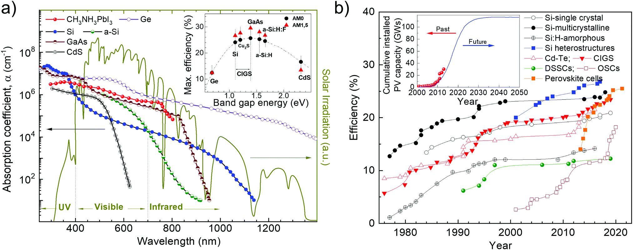 | ||
| Fig. 1 (a) Light wavelength (λ) dependence of the absorption coefficient (α) at room temperature (RT) of some semiconductor materials used in PV technologies. The inset shows the maximum theoretical solar-to-energy conversion efficiency (ηth) of SCs under AM 1.5 light radiation determined by the S–Q limit. Adapted from: ref. 47 and 48. (b) Description of the development of laboratory SCs. Inset: Cumulative installed PV capacity and plausible projection in the near future. Adapted from: ref. 63, 64 and 65. | ||
The growth of the global market share of PV technology has been impressive and the demand for cumulative solar PV electricity generation is expected to move toward the scale of hundreds of gigawatts in the near future (Fig. 1b),63–65 with η of 2nd- and 3rd-generation SCs surpassing that of c-Si (Fig. 1b, inset panel).
Fundamentally, an ideal photoactive material for SCs based on thin films has to be a direct-bandgap semiconductor with an Eg in the 1.0–2.0 eV range to absorb sunlight in a wide spectrum range.46 Moreover, it should have high charge carrier mobility (μ)66 and should be compatible with one or the other material constituting the cell architecture to form reliable electrical connections.67 Notably, the optical penetration depth (δp), (i.e., the spatial region in which most of the incoming photons are absorbed to produce charge carrier pairs) of the photoactive material is crucial to determine its thickness (t). In fact, δp can be approximated to α−1, in agreement with the Lambert–Beer law: Tr = (I/Io)·e−αt, in which Tr is the optical transmission, while I and Io are the intensity of transmitted and incident light, respectively.68 Consequently, the most appropriate t value of the photoactive material should be as close as possible to the value of α−1, to facilitate charge transport toward the external circuitry, without significant charge recombination losses.
Following the research effort on graphene,69,70 the development of other layered two-dimensional (2D) materials (named graphene-related materials (GRMs)),71,72 as well as other 2D materials (e.g., nonlayered 2D materials and 2D perovskites), has burgeoned into the field of SCs and optoelectronic applications. In particular, graphene opens endless possibilities for new generations of SCs owing to its outstanding (opto)electronic properties (e.g., low sheet resistance (Rs ≈ 6.45 kΩ □−1),73 excellent optical transparency in the UV-to-IR region (Tr > 97.7%),73 high intrinsic strength (∼130 GPa), high Young modulus (∼1 TPa), high electron mobility (μe) (>105 cm2 V−1 s−1),71 large specific surface area (SSA) (∼2630 m2 g−1),74 and excellent chemical stability and catalytic activity toward photo(electro)chemical cell-related redox reaction.75–77 Moreover, the (opto)electronic properties of graphene can be tuned via its chemical functionalization processes.78–80 In this context, graphene oxide (GO) (i.e., graphene with C–O bonds and functionalities, such as –OH, C![[double bond, length as m-dash]](https://www.rsc.org/images/entities/char_e001.gif) O, and COO– groups)81,82 or reduced graphene oxide (RGO),83 as well as mono- and few-layered GRMs, exhibit electronic84–86 and optical properties87,88 that are complementary to the graphene ones. Among GRMs, transition metal dichalcogenides (TMDs) with the general stoichiometry of MX2, where M is a transition element of groups IVB–VIIB and X is a chalcogen (i.e., S, Se, and Te) (Fig. 2), strongly emerged for their potential exploitation in the development of novel SCs due to their physical properties.89–91 For example, together with graphene and graphene derivatives, TMDs are becoming attractive candidates as electron/hole transporting materials in several types of SCs92 due to their electronic structure capable to optimize charge transport toward the current collectors.93,94 Overall, the field of 2D materials is an ever-expanding research area, and new GRMs (e.g., metallic group-V TMDs,95,96 transition metal monochalcogenides (TMMs),97,98 MXenes,99,100 silicene,101 phosphorene,102 antimonene,103 bismuthene,104,105 arsenene,106 and graphdiyne107,108) and even other types of synthetic 2D materials (not strictly belonging to the class of GRMs) are rapidly coming into the fray. Finally, the scenario of solution-processed 2D materials for PVs and, in general, optoelectronic applications, has been recently extended to both nonlayered 2D materials109 and 2D perovskites.110,111 In their review article,112 Liu et al. outlined the advent of 2D materials for several PV technologies, showing the most important achievements up to 2015. It is now crucial to provide an update on the use of 2D materials in SCs, including OSCs, DSSCs, PSCs, QDSCs, organic–inorganic hybrid SCs, as well as tandem systems.
O, and COO– groups)81,82 or reduced graphene oxide (RGO),83 as well as mono- and few-layered GRMs, exhibit electronic84–86 and optical properties87,88 that are complementary to the graphene ones. Among GRMs, transition metal dichalcogenides (TMDs) with the general stoichiometry of MX2, where M is a transition element of groups IVB–VIIB and X is a chalcogen (i.e., S, Se, and Te) (Fig. 2), strongly emerged for their potential exploitation in the development of novel SCs due to their physical properties.89–91 For example, together with graphene and graphene derivatives, TMDs are becoming attractive candidates as electron/hole transporting materials in several types of SCs92 due to their electronic structure capable to optimize charge transport toward the current collectors.93,94 Overall, the field of 2D materials is an ever-expanding research area, and new GRMs (e.g., metallic group-V TMDs,95,96 transition metal monochalcogenides (TMMs),97,98 MXenes,99,100 silicene,101 phosphorene,102 antimonene,103 bismuthene,104,105 arsenene,106 and graphdiyne107,108) and even other types of synthetic 2D materials (not strictly belonging to the class of GRMs) are rapidly coming into the fray. Finally, the scenario of solution-processed 2D materials for PVs and, in general, optoelectronic applications, has been recently extended to both nonlayered 2D materials109 and 2D perovskites.110,111 In their review article,112 Liu et al. outlined the advent of 2D materials for several PV technologies, showing the most important achievements up to 2015. It is now crucial to provide an update on the use of 2D materials in SCs, including OSCs, DSSCs, PSCs, QDSCs, organic–inorganic hybrid SCs, as well as tandem systems.
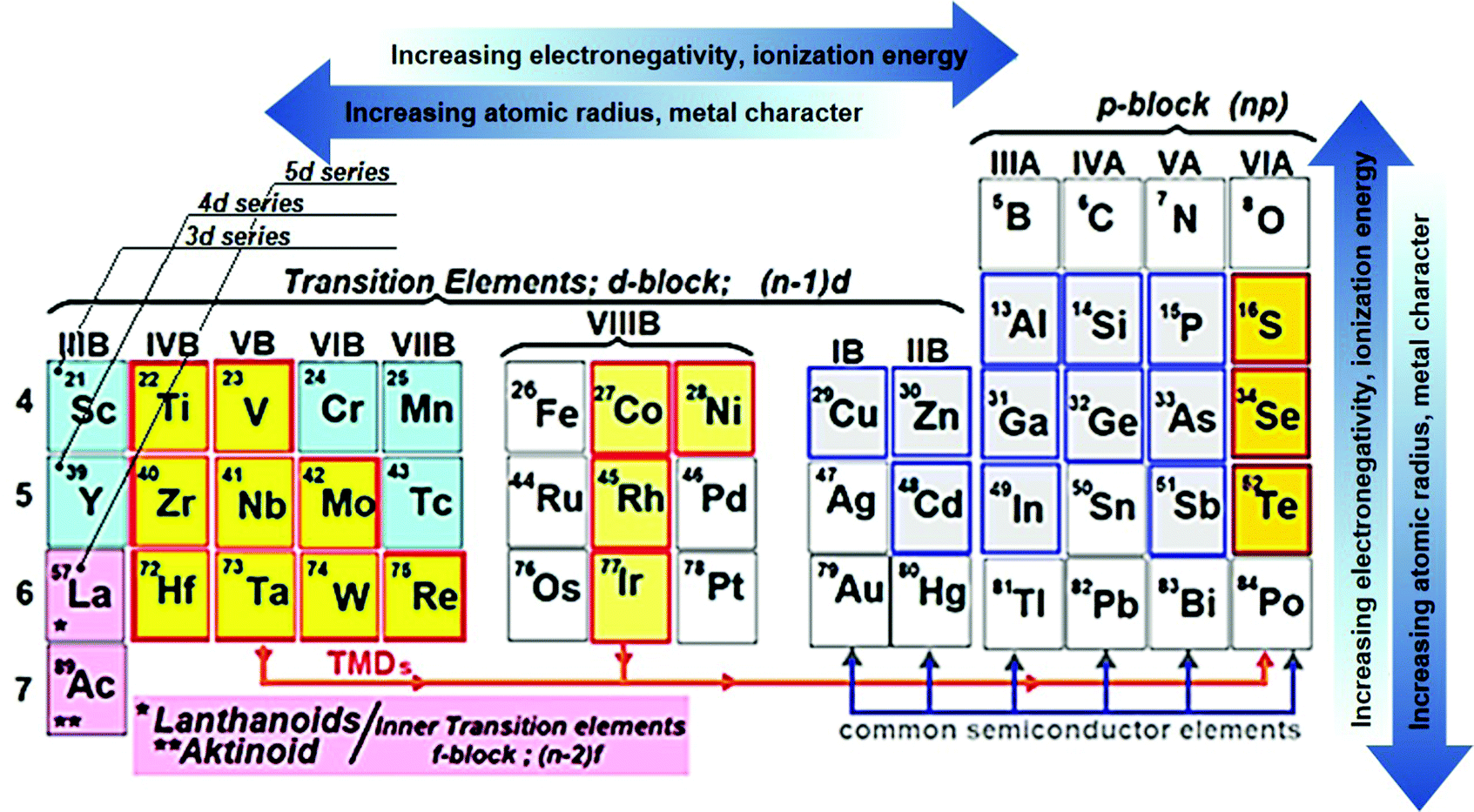 | ||
| Fig. 2 Selected elements across the periodic table that—as a single element (e.g., Si, Ge), compounds (e.g., GaAs, CdAs), or alloys (e.g., SixGe1−x, AlxGa1−x)—display semiconductor nature (into the blue frame) and the transition metals and three chalcogen (X) elements (enclosed by a red frame) that predominantly crystallize in layered TMDs. Partial highlights for Co, Rd, Ir, and Ni indicate that only some of their TMDs form layered structures. | ||
The production of 2D materials by solution processing83,113 represents an ideal platform for the advancement of PV technologies. In fact, liquid-dispersed 2D materials can be produced with on-demand morphological properties, i.e., lateral size114,115 and thickness116–118 by exploiting sorting, or can be chemically modified to tuning the (opto)electronic properties.119 Moreover, 2D materials produced by solution processing can be used for the realization of composites,120i.e., blending with polymeric matrices, and the production of films by means of several coating techniques, such as inkjet121,122 and screen123,124 printing, drop125 and dip126 casting, and spin127,128 and spray129,130 coating.
The possibility to produce and process 2D materials and their heterostructures in the liquid phase represents a step forward toward the development of industrial-scale, reliable, inexpensive printing/coating processes, which can ultimately lead to a reduction in the levelized cost of energy (LCOE) of current PV technologies (less than 5 US cents kW h−1)131–133 to compete with fossil fuels.134,135
In this review, Section 2 provides an overview of the structural and (opto)electronic properties of 2D materials, highlighting the differences of GRMs compared to their bulk counterparts. The production and processing of GRMs in the liquid phase is thoroughly discussed in this section. A brief paragraph focuses on 2D nonlayered materials, while a specific discussion on 2D perovskites is provided in the section related to PSCs (i.e., Section 6). In Section 3, we introduce the main figures of merit (FoM) of SCs and SC components to facilitate the discussion and understanding of subsequent sections. The use of solution-processed 2D materials as building blocks in OSCs, DSSCs, PSCs, and other types of SCs (i.e., QDSCs and organic–inorganic hybrid SCs) is presented and critically discussed in Sections 4, 5, 6, and 7, respectively. Finally, Section 8 summarizes the key results of solution-processed 2D materials in PV technologies, providing the status, prospects, and challenges in this field.
2. Basic properties, production, and functionalization of 2D materials
2.1 Basic properties of GRMs
As depicted in Fig. 3a, graphene is a one-atom-thick layer of carbon atoms bonded together in a hexagonal honeycomb lattice.136 Owing to its unique physical and chemical properties,71 it became highly attractive for fabricating conductive and transparent thin films,73 even though numerous other (opto)electronic73 and ECS5,137 applications exist. Graphene can be considered as the starting material for all fullerene allotropic dimensionalities, including spherical buckyballs (zero-dimensional, 0D), one-dimensional (1D) carbon nanotubes (CNTs), further categorized in single- and multiwalled CNTs (SWCNTs and MWCNTs, respectively) depending on the number of graphene layers, as well as charcoal and graphite.138 | ||
| Fig. 3 (a) Schematic of the honeycomb graphene network as formed by C atoms and bonded basal σ bonds perpendicular to π orbitals. The other graphene-derived allotropes of C are also shown. Adapted from ref. 139 and 140. (b) Band structure in the honeycomb lattice. In the enlarged picture, the energy bands close to one of the Dirac points are also sketched. Adapted from ref. 141. | ||
Graphene nanoplatelets (GNPs), i.e., flakes of functionalized graphene with a thickness ranging from ∼2 to ∼15 nm and a lateral size ranging from the submicrometer scale to 100 μm,137 and (R)GO, obtained by chemical/thermal processes,82,83 are the most frequently used graphene derivatives for large-scale industrial applications, including composites142–145 and ECS devices.5,137,142,146,147 There is a large number of studies that detail the properties of GRMs.71,137,148 Therefore, herein, we briefly focus only on the most peculiar properties of graphene, as well as those of other layered materials. Single-layer graphene (SLG) is a “zero-bandgap semiconductor” with the valence band (VB) and conduction band (CB) touching at the Dirac points (see Fig. 3b)148,149 and charge carriers that can be regarded as mass-less electrons or Dirac fermions.148 Electron mobilities exceeding 2 × 105 cm2 V−1 s−1 at charge carrier densities of ∼2 × 1011 cm−2 have been reported by Bolotin and co-workers by suspending SLG above a Si/SiO2 gate electrode.150 However, it has been shown that graphene on SiO2 has a μ value that is limited by scattering from charged surface states and impurities,151–154 SiO2 surface optical phonons,153,154 and substrate surface roughness.155–157 By searching for alternatives to SiO2, it has been demonstrated that hexagonal boron nitride (h-BN), an insulating isomorph of graphite with B and N atoms and a small lattice mismatch (1.7%) relative to graphite,158 represents an ideal, flat dielectric substrate for graphene.159,160 Thus, graphene on h-BN can reach a μe value exceeding 6 × 105 cm2 V−1 s−1,159 which is 3 times higher than those shown on SiO2. These results suggest graphene to be an ideal channel material for the fast transport of charge carriers in nanostructured and thin-film electrodes.161,162 As a comparison, μ of graphene is ∼200 times higher than that of Si (∼1400 cm2 V−1 s−1).163
Graphene, owing to its mechanical properties (i.e., flexibility and stretchability),71 is an ideal material to fabricate flexible and ultralight devices.164–167 It is important to highlight the dependence of the (opto)electronic properties (e.g., Rs and Tr) on the number of graphene layers. In fact, by investigating the dependence of the Tr value of graphene on the number of layers, Nair et al.168 reported that the opacity of graphene increases by ∼2.3% for each added layer. Moreover, Li and co-workers169 measured a Rs value that varies from 2.1 kΩ □−1 to 350 Ω □−1, moving from SLG to 4-layer graphene, while Tr is reduced to ∼90% (at λ = 550 nm) for 4-layer graphene (Fig. 4).
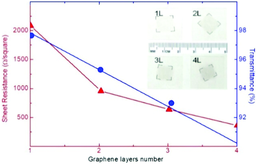 | ||
| Fig. 4 Sheet resistance (Rs) and transmittance (Tr) of a graphene (film) as a function of the number of stacked graphene layers. Adapted from ref. 169, Copyright 2008, American Chemical Society. | ||
Overall, the aforementioned properties make graphene, as well its derivatives, a distinctive material for PV applications. In fact, low Rs, large SSA, and high μ and Tr are essential requirements to be considered in the choice of material for the various building blocks of SCs. Beyond graphene, there is a plethora of other 2D materials that range from insulators (e.g., h-BN) to semiconductors (e.g., TMDs, such as MoS2 and WS2, and phosphorene), metals (e.g., TiS2 and several group-5 TMDs, such as 2H- and 3R-TaS2, 2H- and 3R-NbS2, and 1T-VSe2), and even superconductors (e.g., 2H-NbSe2) and charge density wave materials (e.g., 1T and 2H-TaS2, 1T- and 2H-TaSe2, 2H-NbSe2, 1T-VS2, and 1T-VSe2) at low temperatures.170–173 In addition, 2D materials, such as Bi2Te3, Sb2Te3, Bi2Se3, SnTe, and even graphene, can display unique symmetry-protected helical metallic edge states with an insulating interior, yielding so-called topological insulators.174,175 As for graphene, research on other GRMs, including TMDs,176,177 TMMs,178–181 transition metal oxides (TMOs),182 monoelemental 2D materials (silicene, phosphorene, germanene, stanene, borophene, gallenene, arsenene, antimonene, bismuthene, plumbene, selenene, and tellurene),183,184 and MXenes,185 have provided evidences that the band structure of such materials drastically changes as they shrink from the bulk to the monolayer due to quantum confinement effects.170,171,186 The abundance of GRMs and the ability to stack them in a layer-by-layer manner in desired sequences, eventually through solution-processed methods, offer the possibility to create novel three-dimensional (3D) architectures with entirely new functions,187,188 which have been foreseen to design the next generation of PV devices.189 In particular, the so-formed heterostructures are held together by van der Waals forces, as occurring in other layered materials. Since the family of GRMs is continuously expanding, the complexity of the heterostructures that can be created is nearly unlimited.190 The stacking of different GRMs can lead to a series of synergistic effects, such as190 (1) charge redistribution between closed materials (and even more distant materials) in the stack; (2) structural changes in the stacked materials, whose ultimate properties depend on their orientation relative to the neighboring materials. In addition to leading to the discovery and observation of novel thrilling physical phenomena, the enormous range of functionalities of 2D material heterostructures has yielded applications in PVs and optoelectronics. For example, photoactive semiconducting layers (e.g., TMDs) have been coupled with graphene as transparent electrodes to form photodetectors.191,192 In addition, the combination of 2D materials with different work function (ϕW) values (such as MoS2 and WSe2) enables photoexcited charges (electron and holes) to be accumulated in different layers, resulting in indirect excitons with long lifetimes and tunable binding energies.193,194 At the atomic scale, p–n junctions (e.g., GaTe/MoS2) have been created to provide highly efficient carrier separation, reaching external quantum efficiency (EQE) higher than 60%.195 The exciting and vast topic of 2D material heterostructures is subject of relevant reviews, for which we refer to more in-depth discussions.187,190,196–199 In the context of our work, it is worth pointing out that the realization of 2D material heterostructures with atomic precision and predetermined features by means of scalable solution-processing methods remains a formidable challenge. Nevertheless, the feasibility of printed heterostructures has been proven by several works,200–204 paving the way toward their integration in advanced energy conversion devices, including SCs.
It is important to point out that GRM films formed by interconnected flakes are commonly proposed as functional components in several massive applications, including energy conversion and storage applications.5 In fact, this approach can be realized by printing GRMs that are produced in the form of inks and pastes by means of scalable methods, such as liquid-phase exfoliation (LPE) (detailed discussion of solution-based syntheses and processing of GRMs is provided in Section 2.4).205 Although, in principle, the properties of each flake can be preserved, the properties of whole films strongly depends on their morphology and structure, which are determined by the orientation and interconnection between the composing flakes. The same flakes can show different lateral sizes, thicknesses, and chemical compositions (in the case of heterogeneous films), resulting in different optoelectronic characteristics.205 For the specific case of graphene flake films, contact resistance between the flakes and poor film compactness drastically decrease the conductivity of films compared to that of SLG and FLG (>10![[thin space (1/6-em)]](https://www.rsc.org/images/entities/char_2009.gif) 000 S cm−1).69 Based on our experience, an as-deposited film of pristine graphene flakes typically shows a conductivity lower than 10 S cm−1, together with poor mechanical properties. In order to strengthen the interconnection among graphene flakes, the incorporation of polymeric binders and other conductive additives, e.g., carbon black, is a common strategy that enables a low-temperature-processed film to achieve conductivity higher than 100 S cm−1.206 In particular, the use of carbon black nanoparticles (NPs) or other carbon NPs is effective to fill the voids of the as-deposited network of graphene flakes, which are consequently electrically bridged.206,207 The application of pressure, as well as thermal treatments, can further increase the conductivity of graphene flake films.208,209 In fact, compression treatments make the graphene-based films denser by decreasing the distance between flakes.208 Meanwhile, thermal treatments can decompose or even evaporate the binders and/or surfactants, which limit the conductivity of the film.209 Similar arguments apply to films composed of flakes of other GRMs besides graphene, although their functionalities can be different from those discussed above for graphene flake films.
000 S cm−1).69 Based on our experience, an as-deposited film of pristine graphene flakes typically shows a conductivity lower than 10 S cm−1, together with poor mechanical properties. In order to strengthen the interconnection among graphene flakes, the incorporation of polymeric binders and other conductive additives, e.g., carbon black, is a common strategy that enables a low-temperature-processed film to achieve conductivity higher than 100 S cm−1.206 In particular, the use of carbon black nanoparticles (NPs) or other carbon NPs is effective to fill the voids of the as-deposited network of graphene flakes, which are consequently electrically bridged.206,207 The application of pressure, as well as thermal treatments, can further increase the conductivity of graphene flake films.208,209 In fact, compression treatments make the graphene-based films denser by decreasing the distance between flakes.208 Meanwhile, thermal treatments can decompose or even evaporate the binders and/or surfactants, which limit the conductivity of the film.209 Similar arguments apply to films composed of flakes of other GRMs besides graphene, although their functionalities can be different from those discussed above for graphene flake films.
2.2 Two-dimensional materials beyond “conventional” GRMs
000 cm2 V−1 s−1 for PbS).235 To date, 2D nonlayered materials have been demonstrated for UV-sensitive photodetectors, reaching a responsivity of up to 3.3 A W−1 for Ga2O3,236 400 A W−1 for α-Bi2O3, and 3.17 A W−1 for γ-CuBr.225 In addition, visible-light photodetectors were successfully achieved using CdTe nanoflakes (responsivity of 0.6 mA W−1),237 ZnTe nanoflakes (responsivity as high as 453.9 A W−1),223 and α-MnS (responsivity of 139 A W−1).238 PbS,239 ZnSb,240 and Te231 nanoflakes were used for IR photodetection, reaching responsivity of 1621 A W−1, 89.2 A W−1, and 13 A W−1, respectively. Finally, CuGaSe2,241 α-In2Te3,242 Pb1−xSnxSe,243 Bi,229,230 In2S3,234 CuInSe2,244 Te,245 and Ge228 have also shown attractive properties for broadband photodetection.109 Beyond the use of single 2D nonlayered materials, more complex photodetectors have been produced by coupling 2D materials, including layered and nonlayered ones, in the form of in-plane and out-of-plane heterostructures. Therefore, novel Schottky structures, p–n junctions, and phototransistors have been successfully proposed, as summarized in ref. 109. The application of 2D nonlayered materials has also been reported, although this technology is still in an early stage of development.109 The progress in the control of unsaturated dangling bonds of 2D nonlayered materials is mandatory for the realization of high-quality PV devices. Recently, CdS/Cu2S heterojunction with a clear PV effect was realized via the cation-exchange protocol, yielding an η value of 2.1% (despite a cell thickness of only ∼30 nm).246 Alternatively, GRMs have been used as an ideal interface for the growth of 2D nonlayered materials.109 Based on this strategy, a PV device was fabricated by directly depositing a thin layer of MoO3 onto MoS2, reaching an η value of 3.5%.247 Despite these progresses, the application of 2D nonlayered materials in prototypical SCs, including 1st-, 2nd-, and 3rd-generation SCs, has not been established yet, probably due to the difficulties in producing 2D nonlayered materials on a large scale.109 Therefore, these materials will not be the specific subject of discussion in the present work. By achieving reproducibility in terms of thickness, crystallinity, and structural properties, their incorporation in practical PV devices could represent a key point to drive PV technologies beyond their current performances.
2.3 Classification of semiconductor 2D materials: n-type or p-type materials?
To provide some guidelines regarding their functional role in SCs, semiconductor 2D materials can be classified depending on their (opto)electronic properties. However, for the case of solution-processed 2D materials, such properties are strongly influenced by both structural and chemical characteristics. The possibility to on-demand tune the (opto)electronic properties by structural and chemical engineering is a key feature of solution-processed 2D materials, making them extremely versatile for application in PV devices. As discussed in the following sections (4, 5, 6, and 7), the structure of SCs is commonly engineered by introducing proper charge transporting layers (CTLs), which efficiently and selectively extract the photogenerated charges, improving the device performances. In this context, it is common to consider p-type and n-type materials to extract holes and electrons, respectively. However, the choice of CTLs can follow more complex rationales. In fact, the charge transporting properties are determined by the entire electronic structure of the materials, as well as by their chemical reactivity with the interfaced materials. As a striking example, MoO3, which can also be found in the 2D form, is a typical n-type material that acts as an efficient hole transporting layer (HTL) due to its high ϕW.287,288 The latter can even be higher than 5 eV,289 similar to that exhibited by common p-type materials used to extract photogenerated holes.290 Therefore, MoO3 can efficiently collect holes from its CB through an electron injection mechanism.291 Furthermore, MoO3 forms a highly p-type-doped interface with active materials having ionization energies lower than ϕW of MoO3, favoring the hole extraction process.291–293 Similar to MoO3, 2D materials can go against the rules “p-type materials collect holes” and n-type materials collect electrons”; therefore, they should be specifically examined to understand their functional role in the SC structure. Based on this consideration, semiconductor 2D materials will not be classified as n-type or p-type materials because there is no a clear one-to-one correspondence between 2D materials and their electronic properties, as well as between the electronic properties of solution-processed 2D materials and their functional role in PV devices.2.4 Solution processing of 2D materials
The design, development, and production of (opto)electronic devices73,86,294,295 inherently depend on the properties of the available materials.83,296 Different methods have been reported for the production and processing of GRMs. The main approaches for the production of GRMs have been summarized in previous works.83,296–298 Although proof-of-concept PV devices have been demonstrated for exploiting micromechanically cleaved materials,299 the discovery of scalable methods to produce GRMs with “on-demand” tuned structural and (opto)electronic properties is a “must” for the realization of practical SCs. The production of large-area, high-quality GRMs is still one of the most urgent needs of this research area,83,296,297 even though several progresses have been accomplished at the industrial level. The requirement to exercise control at the monolayer level needs the understanding of surface physics and chemistry, which has so far not been fully demonstrated in any multicomponent materials system. For example, progress is being made toward the production of large-area single crystals,297,300–306 a key process for the development of high-quality thin films with both optical transparency and electrical conductivity.307,308 Growth techniques reported in the literature for 2D materials, e.g., chemical vapor deposition (CVD), molecular beam epitaxy (MBE), and atomic layer deposition (ALD), have been conventionally used to create heterostructures based on graphene, other elemental 2D materials, TMDs, TMOs, h-BN, and oxide materials.83 For example, significant progresses have been made in the growth of graphene on metals309 and on silicon carbide (SiC).83,310,311By carefully choosing the individual components, one can tune the growth/production parameters, creating GRMS “on demand” for the design and realization of van der Waals heterostructures with functional properties.187,312,313 However, the growth of 2D materials by means of the aforementioned synthesis routes is challenging in the case of nonmetallic substrates.314 In order to exploit the availability of high-quality synthetic 2D materials for practical devices, the transfer and alignment processes of 2D films on arbitrary substrates have to be developed. Several transfer processes classified as wet- or dry-transfer have been proposed and utilized so far.83,297,305,315–319 In the wet-transfer process, the as-grown 2D material contacts the liquid during at least one step of the process.83 This determines the occurrence of adsorbates that are trapped onto the 2D materials surface, significantly influencing the interface quality. To avoid this drawback, dry-transfer processes have been established to create perfectly clean interfaces.83,320 This has been a crucial step for the demonstration of the fundamental properties of 2D materials, which requires extremely low densities of interface traps and dangling bonds.321
Recent reports on the dry transfer of graphene using pick-and-place techniques322 and exploiting h-BN as the 2D dielectric have successfully achieved extremely high μ (i.e., 350000 cm2 V−1 s−1) in graphene.323 However, transfer processes intrinsically represent limitations for the integration of high-quality 2D materials in practical devices, in which direct material growth on ad hoc materials and/or solution-based processing are required for the realization of high-throughput device manufacturing chains. Recently, the direct growth of graphene on glass, creating the so-called “super graphene glass,” has attracted enormous interest to circumvent transfer-process-related issues for practical applications,324–327 including transparent conductors, smart windows, simple heating devices, and SC electrodes. However, the CVD growth of high-quality graphene is still challenging, and “super graphene glasses” currently show (opto)electronic properties still far from those of CVD graphene grown on metallic substrates.324 In fact, on a catalytically inert glass surface, one cannot expect yet to control the graphene growth as done onto a catalytically active metal surface.83
The direct exfoliation of bulk layered crystals by LPE328–330 is an industrially relevant strategy for the scalable production and/or processing of GRMs. Herein, we will summarize the main methods for the production and processing of 2D materials in solution, while additional details can be found in recent literature reviews.83,205,297,298,331 The LPE process enables the formulation of inks of GRMs in different solvents (Fig. 5a).332–335 This is the starting point for the reliable production of devices based on printed technologies,333 as well as for targeting the industrial fabrication of GRM-based devices, including SCs (Fig. 5b).205
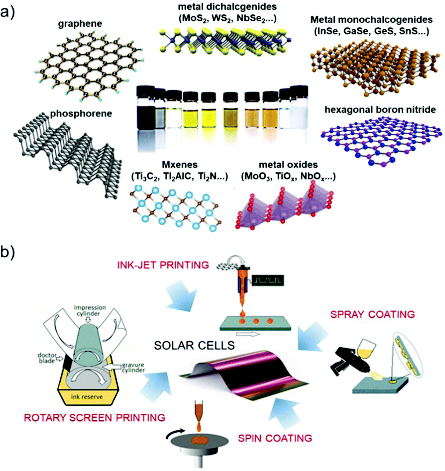 | ||
| Fig. 5 (a) Schematic of monolayer materials, e.g., graphene, elemental 2D materials (phosphorene), metal dichalcogenides, metal monochalcogenides, MXenes, h-BN, and metal oxides, and their formulation in the form of ink. (b) Schematic of solution-processing methods of SCs, including relevant material deposition techniques (e.g., spin coating, spray coating, inkjet printing, and rotary screen printing). | ||
Liquid phase exfoliation is a versatile technique and it has been established for the exfoliation of numerous layered materials,328–330 including graphite, TMDs, TMMs, black phosphorus (BP), and h-BN, just to cite a few. As depicted in Fig. 6, the liquid-phase processing of bulk layered crystals generally involves (1) the dispersion of bulk crystals in a solvent; (2) the exfoliation of bulk crystals through (acoustic) cavitation or shear forces (Fig. 6a); (3) the “sorting” (e.g., by ultracentrifugation) of the material flake sizes (Fig. 6b).83,205
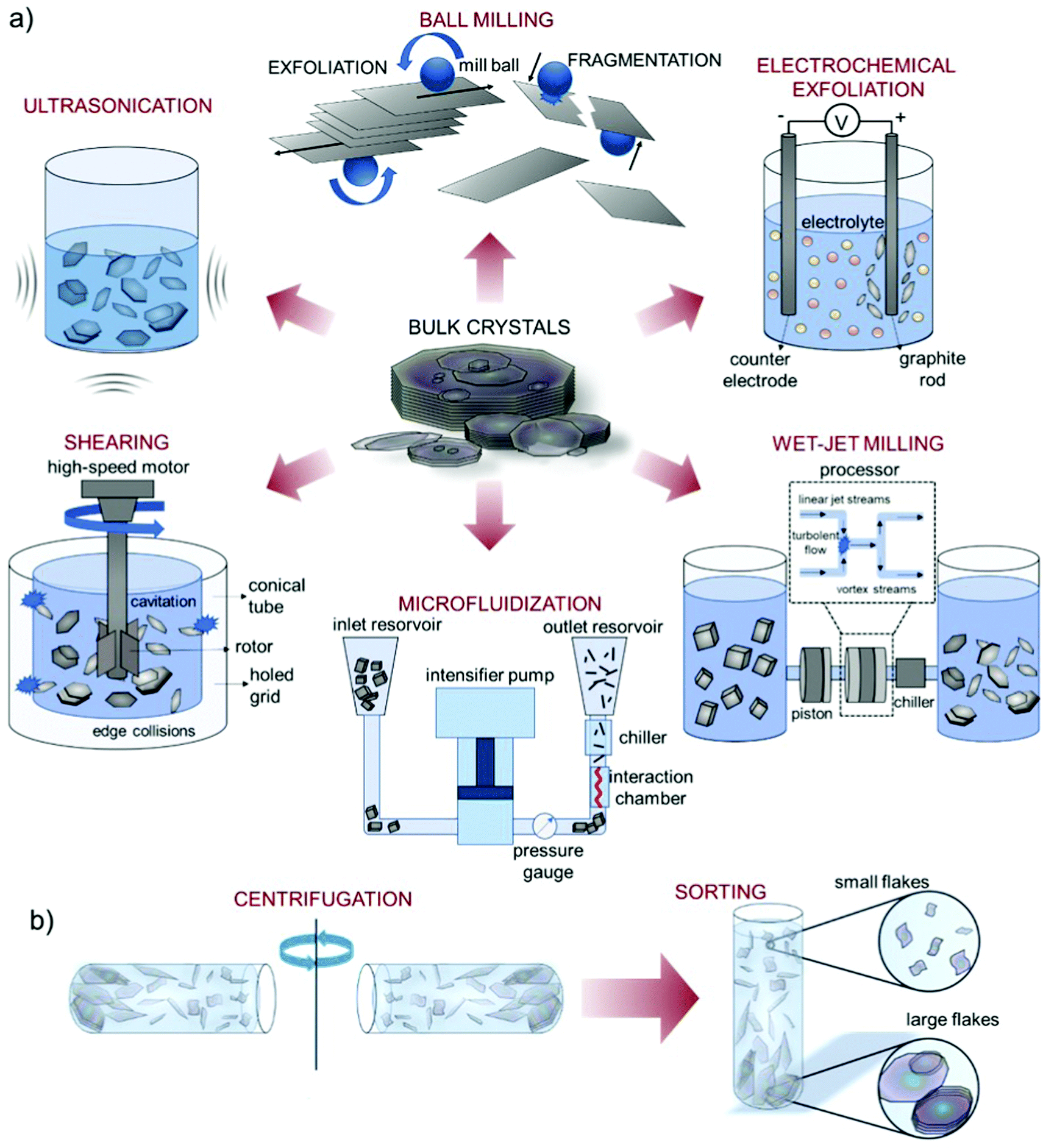 | ||
| Fig. 6 Schematic of the LPE processes. (a) Schematic of various LPE methods reported in the literature, including ultrasonication, shearing, wet-jet milling, microfluidization, ball milling, and electrochemical exfoliation. Schematic of the LPE methods adapted from ref. 336, 356, 360. (b) Dispersion purification by means of ultracentrifugation (sedimentation-based separation (SBS), and subsequent “sorting” of different material flake sizes. Adapted with permission from ref. 337, Copyright 2017, American Chemical Society. | ||
In general, the LPE process starts with the dispersion of bulk crystals either in organic solvents330 or in aqueous solutions, the latter with the aid of surfactants329,338,339,340 or polymers.341,342 The exfoliation process is commonly carried out by exploiting cavitation328–330 or shear forces343 to produce single- and few-layer materials.344 Ultrasonication-assisted exfoliation of bulk crystals is the prototypical LPE method.328,329,345–349
For the case of graphene, the ultrasonication process produces defect-free flakes (i.e., no additional defects are introduced during exfoliation) as well as achieves concentrations of several grams per liter.350 However, ultrasonication-assisted LPE is not a scalable process, since it is a time-consuming process requiring several hours.205 Other approaches have also been proposed, such as ball milling,351–353 shear exfoliation,354,355 and microfluidization.356–359 All these approaches have pros and cons compared with the ultrasonication method,205 even though some of the apparatus can yield high-throughput production of 2D materials for industrial applications. Recently, Bonaccorso and co-workers presented a novel approach to exfoliate layered crystals, i.e., graphite, h-BN, and TMDs, based on the high-pressure wet-jet milling (WJM) technique.360 In detail, during the WJM process, a hydraulic piston applies a pressure between 180 and 250 MPa, forcing the solvent/layered-crystal mixture to pass through perforated disks with variable diameters (typically between 0.3 and 0.1 mm), called the nozzle. This process generates shear forces that promote the exfoliation of layered materials.359,361 The key advantage of the WJM technique compared to other LPE methods is the small time required to process the sample, which is reduced to less than one second, instead of the several hours required during ultrasonication-assisted exfoliation328,329,344–348 or shear exfoliation.353,354 By means of the WJM method, a production rate higher than 2 L h−1 of 2D crystal dispersion (concentration: 10 g L−1) and an exfoliation yield (defined as the ratio between the weight of the exfoliated material and the weight of initial graphite) of 100% have been demonstrated with a single WJM apparatus.359,362 The 2D crystals obtained through WJM have already been used for a wide range of ESC applications363–371 and composites,372 in which a large volume of material is needed for their industrial implementation. Another approach to upscale the 2D material production (beyond tens of grams per hour) is the electrochemical exfoliation process. In this method, a potential difference is applied between a layered anode/cathode in an electrolyte-containing medium.373–375 In these experimental conditions, positive or negative charges can be imparted to the layered materials, promoting the intercalation of oppositely charged ions and facilitating the exfoliation process.372–374 These processes can be broadly classified in two classes. The first one is the anodic exfoliation in the inorganic salts’ aqueous solution, mineral acids, or mixture of water and ionic liquids. The second one is the cathodic exfoliation in organic solvents (e.g., N-methyl-2-pyrrolidone, dimethyl sulfoxide, and propylene carbonate) in the presence of alkylammonium salts or Li.374 Electrochemical methods are extremely attractive since they reduce the use of chemical oxidants as the driving force for intercalation or exfoliation, and the electromotive force is controllable for the creation of tunable-material intercalated compound.372–374 In addition, the extensive capabilities of the electrochemical exfoliation method to modify materials enables the facile and direct synthesis of functionalized 2D materials with the desired properties for composites, electronics, and ECS applications.372–374 Regardless of the LPE process used to produce 2D materials, a common key issue of the aforementioned methodologies is that the resulting samples are polydisperse in their dimension, typically showing broad distributions of flake thickness and size.205,297 Thus, it is crucial to obtain a fine adjustment of the morphological properties by separating small from large flakes337 and thin from thick ones.339 This step is typically performed using ultracentrifugation protocols.339,376–381 In this context, exfoliated GRMs can be sorted with respect to thickness and lateral size using techniques based on ultracentrifugation in uniform media (SBS)382 or density gradient media (density gradient ultracentrifugation (DGU)).381
Another important issue of 2D flakes produced in the form of ink through LPE methods is the re-aggregation of flakes after their deposition/coating. In fact, flake re-aggregation might affect the electronic (i.e., μ, contact resistance) and physical (i.e., roughness) properties of the resulting films. Therefore, suitable strategies must be developed to minimize flake reaggregation with regard to practical applications. For example, the addition of stabilizers (e.g., surfactants and polymers) physically hinders flakes’ contact,337–339 impeding their aggregation.337–339 However, the effect of such stabilizers could affect the electrical performance of the assembled films.297,383,384 In addition to the aforementioned issues, some layered materials, such as BP, are unstable under ambient conditions or in the presence of water and/or oxygen.385,386 The instability issue, which might be valid for 2D materials either grown by the bottom-up approach (e.g., CVD)83,387,388 or produced by micromechanical cleavage,69,389,390 can be eliminated by introducing a solvent shell,205 or residual surfactants/polymers adsorbed onto the surface of flakes. Importantly, solvents or surfactant residuals may imply an intrinsic doping of the flakes.205 These effects can be advantageously used to attain controllable doping strategies. The LPE process can also be exploited for the exfoliation of bulk layered materials specifically prepared/synthetized with the desired chemical characteristics (e.g., doping), as for the case of graphite oxide391 (i.e., to produce GO).83,330 In particular, graphite oxide can be prepared by means of chemical processes that introduce functional groups both at the edges (e.g., COOH and CO) and on the basal plane (e.g., OH or epoxide groups).81,82 The occurrence of these functional groups is fundamental toward the production of GO using well-established methods, including thermal expansion,392 ultrasonication,393 and stirring394 of graphite oxide. Moreover, the presence of the aforementioned functional groups introduces polarities395–397 that facilitate the dispersion of exfoliated graphitic materials in aqueous solutions.392,398 Although GO flakes can have lateral sizes up to several microns,399 they exhibit a high density of structural defects,393 which arise from the chemical treatment disrupting the sp2-bonded network.83 Thus, in order to restore both electrical and thermal conductivities of pristine graphene, various strategies have been developed to reduce GO flakes using either chemical397 or physical393,397,400 processes. These reduction processes are imperative to produce a sample of the quality approaching that of pristine graphene. Recently, tremendous progresses have been achieved in this direction, with the demonstration of μ exceeding 1000 cm2 V−1 s−1 in field-effect transistors with microwave-reduced GO.401
Owing to its scalability and cost-effectiveness, LPE techniques can provide GRMs in massive quantities at an accessible price. Moreover, solution-processed 2D materials can be combined with polymeric materials, while being processed in the form of a coating on different substrates. In this context, progresses have been made on the large-scale placement of 2D material-based inks by means of different deposition/coating systems, such as Langmuir–Blodgett,402 spin,403–405 spray,406–408 and rod73 coating; vacuum filtration;409–415 and inkjet,332,333,416 gravure,417 flexographic,418 and screen419 printing (including their roll-to-roll (R2R) configurations).420 Advances in this area enabled the layer-by-layer printing of different 2D material-based films, as well as heterostructures and/or heterogeneous structures, on large areas (ranging from the scale of square centimeters to square meters).205 However, beyond uniformity, the roughness of the deposited large-area films is a critical issue, which may degrade the (opto)electronic properties expected from heterostructures produced through material transfer after micromechanical cleavage or direct growth.187 However, different from the transfer approach, drop-on-demand printing could meet the large-scale fabrication requirements of practical devices.205 For example, drop-on-demand inkjet printing has been demonstrated for the realization of all-printed, vertically stacked transistors with a graphene source, drain, and gate electrodes; a TMD channel; and an h-BN separator.421 The proposed printed device, based on 2D material heterostructures, has shown a μ value of 0.22 cm2 V−1 s−1.420 Despite these important achievements, the obtained μ value is rather low, meaning that further insights are still needed into the assembly of such printed heterostructures.187,332 Here, the challenges to be tackled are two-fold: (1) the optimization of ink formulation fulfilling the morphological (e.g., thickness and lateral dimension of the flakes) and rheological (e.g., viscosity and surface tension of the dispersions) property requirements; (2) the optimization of printing parameters for the deposition of uniform 2D material films with high-quality (i.e., clean) interfaces.205 Noteworthily, the surfaces of 2D materials are strongly affected by both solvent and additive (i.e., stabilizers) residuals,205 which, therefore, need to be minimized. Here, a balance must be found between the possibility to have a clean interface and the intrinsic doping (determined by the presence of solvent and additive residuals) on a case-to-case basis, depending on the final application. Overall, notwithstanding the scalable production of GRMs and their film deposition, understanding the precise determination of crystal structures and their crystallographic relationships is of utmost importance for the design and realization of any (opto)electronic device, including PV ones that are discussed here. Further, chemical doping and functionalization are pivotal to properly tune the (opto)electronic properties of the structures.344,422–425 Both covalent and noncovalent functionalizations introduce a systematic modification of 2D material properties to control their solubility/processability, the prevention of flake re-aggregation, and their (opto)electronic characteristics (e.g., Eg).344,421–423 The chemical modification/functionalization also allows the properties of 2D materials to be combined with the property portfolio of other compounds.344,420 Overall, a thorough understanding of the charge transport and transfer properties, defects (including edge terminations, dopants, point defects, and grain boundaries), environmental contaminants (e.g., surfactants and adsorbates), and chemical reactivity is crucial for the design of practical GRM-based devices.
2.5 Functional roles of solution-processed 2D materials
The understanding of “how to use 2D materials in SCs” is not trivial, since their versatility resulting from the immense portfolio of their (tunable) properties can lead to apparently contradictory experimental results. In fact, there exist solution-processed 2D materials that have been applied to collect either photogenerated holes or electrons, while being used as buffer layers to stabilize the interfaces between the materials comprising the SCs, or even as catalysts for the redox reactions involved at the counter electrodes (CEs) in DSSCs, or as electrically conductive materials for current collectors. This aspect is so surprising to the extent that it could even be disappointing, albeit it reveals the easiness to incorporate 2D materials in SC structures to improve their performances. Scheme 1 reports a sketch of the various functional roles of material components in SCs, as they will be detailed for each type of technology in the subsequent sections. Clearly, solution-processed 2D materials have been applied almost everywhere, most of them for more than one functionality. The most representative example material class, namely, “graphene and its derivatives,” has been used for all the functional roles identified here, indicating the importance to specify the structural, morphological, and chemical properties for each material, thereby using a “case-by-case approach.” In addition, this point implicitly stresses the importance of providing a full set of experimental characterizations of 2D materials when used in SCs, so that it is possible to uniquely correlate their functional role to their intrinsic attributes. Even though it is common to refer to electronic structures of 2D materials in ideal stoichiometry to explain their functional role in SCs, it is recommended to provide experimental measurements (beyond those which are used for the characterization of SCs) to confirm the absence of a relevant discrepancy compared to such ideal cases. In fact, defects, surface oxidation, chemical functionalization, and even the simple morphology of 2D materials can result in optoelectronic properties that are completely different from those of their ideally stoichiometric structures. Examples of effective characterizations are absorbance/reflectance measurements coupled with ultraviolet photoelectron spectroscopy and Kelvin probe measurements to provide the first sketch of the energy-band edge positions and WF values of the materials used in the different components of SCs. Possible discrepancies should be explained by investigating the chemistry of the material surface through X-ray photoelectron spectroscopy (XPS). The impact of 2D morphology on the functional role of 2D materials should be supported by proper lateral and thickness analyses through transmission electron microscopy (TEM), atomic force microscopy (AFM), and surface area measurement techniques (e.g., physisorption characterizations), while the structural properties of 2D materials can be rapidly assessed by both Raman spectroscopy and X-ray diffraction (XRD) characterizations. Electrical and photoelectrical properties, such as (photo)resistivity/(photo)conductivity, of 2D materials could be accessed by realizing and characterizing complementary devices, such as field-effect transistors, as well as a simple four-probe method. These considerations indicate the key importance of providing reliable insights into the nanomaterials, devoted to improve the performance of entire PV systems, which must be carefully rationalized through in-depth experimental characterization. In this context, the efforts recently made to standardize the sequence of methods for characterizing the structural properties of graphene, bilayer graphene, and graphene nanoplatelets in both powder and liquid (i.e., dispersion) forms are noteworthy. The need of such a standard, namely, ISO/TS 21356-1:2021, emerged from the confusion around the terminology of “graphene” used to label commercially available materials. In conjunction with the international ISO/IEC terminology, the ISO/TS 80004-13:2017 standard represents a step forward to the use of (solution-processed) 2D materials with well-defined properties in both laboratory and commercial applications, including SCs.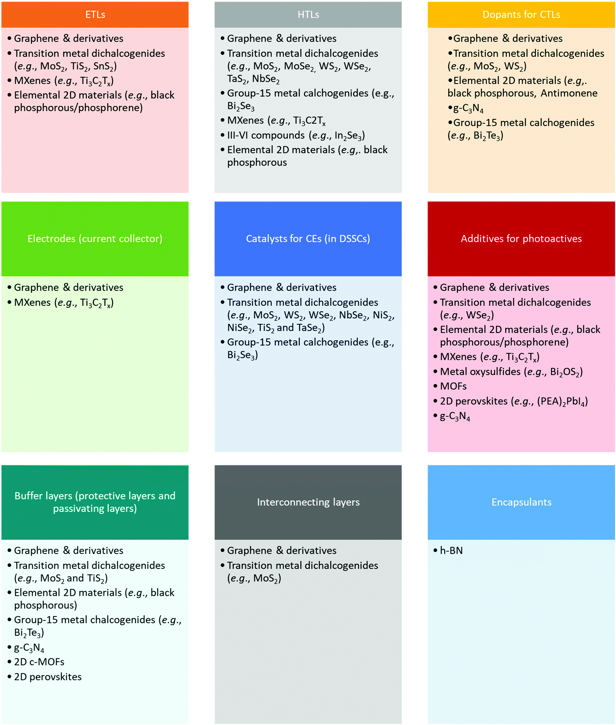 | ||
| Scheme 1 Functional components of SCs and the corresponding 2D materials reported in the literature for such a role. The 2D materials listed here correspond to those reported in the subsequent sections for each type of SC technology reviewed in this work. | ||
3. Figures of Merit of Solar Cells
For facilitating comparison, SCs are often ranked in terms of the following FoM:53(i) EQE, which represents the ratio between the number of charge carriers collected by the cell and that of photon flux (of a given energy) that strikes the cell, i.e.,
 | (3.1) |
(ii) Internal quantum efficiency (IQE), i.e., the fraction of absorbed photons converted in I, i.e.,
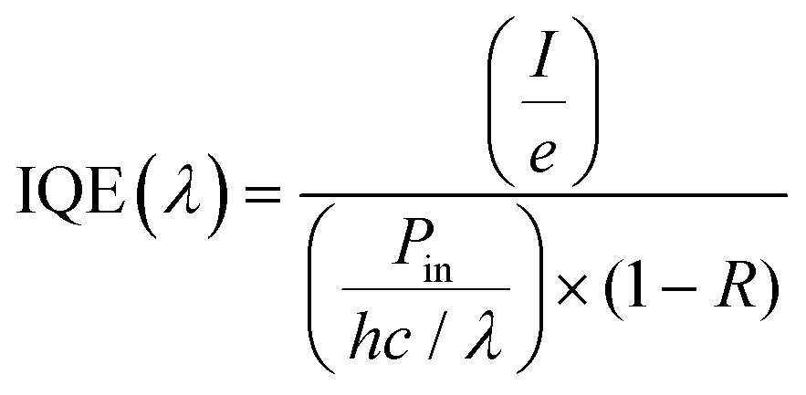 | (3.2) |
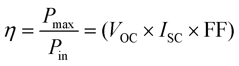 | (3.3) |
 | (3.4) |
Since the application of solution-processed GRMs as transparent conductive electrode (TCEs) for SCs will be examined here, the FoM determining the quality of TCEs are also reported and discussed. The quality of TCEs is mainly assessed through two crucial parameters: Rs and Tr, which should be <10 Ω □−1 and >90%, respectively.73 Moreover, a trade-off between Rs and Tr is unavoidable for TCEs. To evaluate TCEs, the following semiempirical FoM has been proposed:426
 | (3.5) |
Notably, Rs depends on both charge carrier density (Nd) and μ (cm2 V−1 s−1),427 as expressed by the following equation:
 | (3.6) |
In order to describe the frequency dependence of the Tr losses in TCEs,428–430 as well as the critical reflection at the air/film/substrate interfaces,431 the following equation for Tr has been proposed (for thickness ≪ λ/2·π·nfilm, where nfilm is the refractive index of the film):
 | (3.7) |
 | (3.8) |
In addition to Rs and Tr, environmental stability and abrasion resistance are also decisive factors to select TCE materials.
For the specific case of DSSCs, for example, the transport of charge carriers from the photoanode to CE is hindered by several resistances.434–437 The latter include the series resistance comprising Rs of TCE and contact resistance of the cell; the transport resistance of electrons in the TiO2 film (RTiO2); the resistance at the TCO/TiO2 contact (RTCO–TiO2); the charge transfer resistance of charge recombination between the electrons in the TiO2 film and ions in the electrolyte (Rrec); the charge transfer resistance at the CE/electrolyte interface (RCT); the charge transfer resistance at the exposed TCO/electrolyte interface (RTCO–electr.); and the Warburg parameter, which describes the Nernst diffusion of active ions in the electrolyte (Zd). Typically, RCT is often dominant among multiple charge transfer resistances. However, in large-area DSSCs, Rs also significantly determines FF losses.438 The smaller the RS, the higher is the FF, resulting in higher η.439–441 Concerning the electrocatalytic activity of CE, RCT can be explained in terms of current density (J), as expressed by the following equation:
 | (3.9) |
4. OSCs
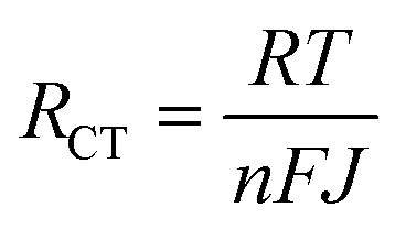
OSCs hold remarkable potential for low-cost, flexible PVs, presenting both compatibility with R2R large-area fabrication443–445 and impressive short-energy pay-back times.446 Bulk-heterojunction (BHJ) OSCs, exploiting blends of p-type polymer (or organic small-molecule) donor/n-type fullerene (or other kind of organic small-molecule) acceptor materials dissolved in a common solvent, have opened an avenue for promising research activity to improve the η value of SCs,447 as well as the overall performance of photoelectrochemical cells.448–455 The BHJ configuration maximizes the donor/acceptor interfacial area, facilitating exciton dissociation and charge transfer by forming a bicontinuous interpenetrated charge transport network in the photoactive layer.456,457 In addition, the incorporation of layers with hole and electron transporting (or blocking) properties between the donor/acceptor active layer and anode/cathode promotes and balances the extraction/collection of photogenerated charges.458 All these properties make the BHJ concept a landmark in OSC development, as well as a plethora of other applications (e.g., photodetectors459 and biosensing devices460–462). Historically, the development of low-bandgap polymers, interfacial engineering, and fabrication techniques allowed BHJ to achieve η exceeding 9% for single-junction cells463–467 and 10% for tandem cells.468 More recently, non-fullerene acceptors (NFAs) have dominated the OSC field due to significant performance and stability improvements.469 Compared with their fullerene-based counterparts, NFAs exhibit tunable bandgaps that extend their light absorption in the NIR region.468 In addition, their tunable energy levels can adjust the energy-level alignments between the constituent layers in OSCs to minimize the energy offsets, increasing the VOC.468 Lastly, their crystallinity can be easily tuned to finely control the photoactive-layer morphology, improving the device stability.470–472 Nowadays, state-of-the-art OSCs exhibit η values over 17% for both single-junction cells and two-terminal tandem cells, mainly due to the rapid developments of NFAs, as well as advanced device engineering.473–477 In particular, the combination of low-bandgap donors and NFA-enabled OSCs has resulted in the achievement of record efficiency of 18.3%.478In a typical OSC structure, GRMs can be incorporated either as additional components or to replace traditional materials, aiming at both performance and stability enhancement. In this context, GRMs have been used to fulfil several functions (Fig. 7) such as (a) transparent front electrode (i.e., TCE)479–481 or back electrode;482–484 (b) electron acceptors in binary OSCs or additives in ternary OSCs in the form of nanoflakes dispersed in donor–acceptor matrices;336,485–487 (c) ϕW-tuned HTLs/ETLs488–490 or interfacial layers in tandem OSCs.491–493 In the following subsections, the application of solution-processed GRMs into OSC structures will be examined for each functional device component.
 | ||
| Fig. 7 Two-dimensional materials used as OSC components, including electrodes, CTLs/buffer layers, and photoactive layers. RGO and electrochemically exfoliated graphene have been used as the TCEs. Functionalized graphene molecules, GO, and TMDs such as MoS2 and WS2 have been investigated as HTLs. Graphene-based molecules, WSe2, and MoSe2 have been used as electron acceptors in binary blends or additives in ternary OSCs. Lastly, OSCs including functionalized graphene or BP as ETLs or interlayers have also been reported. | ||
4.1. TCEs
Graphene has been largely investigated as the TCE in OSCs to replace traditional ITO electrodes. Actually, ITO is currently the most established TCE material for rigid OSCs due to its excellent conductivity (i.e., Rs < 10 Ω □−1 for 100 nm-thick films)495 and high Tr (>80%) in the visible spectrum. However, some drawbacks, including the scarcity of In, expensiveness of the sputter deposition processes, and its polycrystalline structure, makes the ITO films brittle when they are repeatedly bent or stretched,496 nullifying their use in flexible OSCs. In addition, it is recognized that ITO elements diffuse through the photoactive layer, leading to a significant decrease in the OSC performance.497–499 Alternative TCEs based on CNTs,500,501 metallic nanowires,502 and conductive polymers503 have been proposed and used in OSCs. However, these TCEs exhibit high surface roughness and/or large Rs, which reduce the reproducibility rate of the devices.499–502Alternatively, TCEs based on graphene rapidly emerged, and several approaches have been implemented to decrease the Rs values of graphene-based TCEs toward commercially competitive values.73 For example, Wang et al. reported poly(3-hexylthiophene):[6,6]-phenyl C61-butyric acid methyl ester (P3HT:PC61BM)-based OSCs incorporating a TCE comprising 4-layer HNO3-doped graphene prepared by a layer-by-layer transfer method.504 An η value of 2.5% was obtained by the additional evaporation of a thin layer of MoO3 over the TCE in order to improve its hydrophilicity and to tune its ϕW from 4.36 to 5.37 eV.503 Currently, the highest η values of 6.1% and 7.1% reported for flexible conventional and inverted OSCs, respectively, have been achieved using graphene-based TCEs produced through the CVD method.505 Notably, these results have been achieved by applying a MoO3 buffer layer onto graphene-based TCEs.504 More recently, η as high as 8.48% has been achieved in tandem OSCs, which combine a wide-bandgap small molecule with low-bandgap polymer using Au-doped single-layer graphene nanoribbons (GNRs) as the TCE.506 Although the CVD is an efficient approach to produce effective graphene-based TCEs,507–509 the transfer process of the as-grown graphene films onto a target substrate is still critical, negatively impacting the manufacturing time and cost. In this regard, the chemical exfoliation of GO through ultrasonication or rapid thermal expansion, followed by reduction with chemical510 or photo-assisted routes,511 is a reliable low-cost top-down alternative approach, compatible with R2R mass production.83 As discussed in Section 2, RGO can be easily produced in bulk quantities in the form of ink, taking advantage of its solubility in common solvents,512 including water. Consequently, there has been an extensive research effort on the use of RGO as TCE in OSCs.513–515 Flexible OSCs based on a RGO film as the TCE were firstly fabricated using P3HT:PC61BM.514 The RGO TCE was produced by spin coating GO flakes over a rigid SiO2/Si substrate. The resulting GO film was then reduced by thermal annealing and transferred onto a polyethylene terephthalate (PET) substrate, yielding the RGO TCE. However, the constructed devices (area: 1 mm2) have shown a low η value (∼0.78%), which was attributed to the low Tr (65%) and high Rs of the RGO films (∼3.2 kΩ □−1) compared with those of the ITO reference (90% and 15 Ω □−1, respectively).
Geng et al.516 realized graphene-based TCEs using chemically converted graphene (CCG). This was produced by the chemical reduction of GO produced in the form of dispersion without the need of dispersants.515 The reduction was accomplished by annealing GO under a vacuum in a furnace tube. This treatment resulted in the recovery of the sp2-carbon networks of the graphene sheets. The CCG films exhibited Rs = 103 Ω □−1 and Tr = 50%. The P3HT:PC61BM-based OSC with CCG-based TCE yielded an η value of 1.01%, which was approximately half that reached by the reference OSC based on ITO.
In the same framework, an efficient reduction method based on laser illumination was demonstrated by Kymakis et al.517 for the fabrication of flexible graphene-based TCEs, which can be spin cast on substrates that are sensitive to temperature. Femtosecond laser-treated RGO (LRGO) films exhibited Tr of 70% and Rs of 1.6 kΩ □−1 and were subsequently incorporated as the TCE in P3HT:PC61BM-based OSCs, yielding an η value of ∼1.1%.516 Additionally, the as-produced graphene-based OSCs were bent to angles up to 135° without η deterioration, which is different from ITO-based OSCs that failed completely at bending angles greater than 65°.518,519
In order to improve the trade-off between Tr and Rs, the use of a mesh structure with periodic lines, as exploited for Cu-based520 and Si-based521 electrodes appeared to be an eye-catching strategy even for graphene-based TCEs. Following this strategy, Rs and Tr of TCEs can be controlled by varying the grid width, spacing, and thickness of the mesh structure.522 Konios et al.523 demonstrated a scalable one-step patterning of RGO films on PET or glass substrates based on femtosecond laser irradiation treatments. The authors proved an accurate control of RGO micromesh (RGOMM) features on both rigid (glass) and flexible (PET) substrates.522 In particular, they obtained a RGO electrode with Tr varying from ∼20% to ∼85% without deteriorating Rs.522 The as-produced RGOMM was then used as TCE in small- and large-area OSCs based on poly[N-9′-heptadecanyl-2,7-carbazole-alt-5,5-(4′,7′-di-2-thienyl-2′,1′,3′benzothiadiazole)]):[6,6]-phenyl-C71-butyric acid methyl ester (PCDTBT:PC71BM), achieving an η value of 3.67% and 3.05% on glass and flexible substrates, respectively.522
More recently, electrochemically exfoliated graphene (e-graphene) was used as an alternative to RGO for TCE, avoiding the need for the harsh conditions necessary for the graphite oxidation step.524 TCEs based on e-graphene were then formed by spray coating e-graphene dispersion.523 The as-produced films exhibited Rs between 520 Ω □−1 (at Tr of 70%) and 180 Ω □−1 (at Tr of 55%).525 The as-produced TCEs were used in a thieno[3,4-b]thiophene/benzodithiophene:phenyl-C71-butyric acid methyl ester (PTB7:PCB71M)-based OSCs, which reached an η value of 4.23%.523 Subsequently, a mixed-dimensional TCE using silver nanowires (AgNWs) and e-graphene was also demonstrated, achieving an η value of 6.57%.525 The addition of e-graphene on the AgNW network led to a decrease in Rs from 78 to 13.7 Ω □−1 and a reduction in film roughness from 16.4 to 4.6 nm.526
Recently, a graphene-based TCE prepared by stacking polyimide on graphene led to an ultraclean graphene surface, allowing the flexible device to reach a record high η value of 15.2% for flexible OSCs.527 Alternative to the use of high-quality graphene, benzimidazole-doped graphene was also proposed to achieve a trade-off between Tr and Rs, enabling the realization of flexible OSC based on a 3-layer benzimidazole-doped graphene-based anode, with an η value of 6.85%.528
Lastly, both coupling of graphene with metallic grids529,530 and graphene/metal hybridization531–534 are currently prevalent strategies used to achieve an optimal balance between Tr (>90%) and Rs (<100 Ω □−1). Table 1 summarizes the main experimental results achieved with OSCs using graphene-based TCEs.
| Material | Usage | Device structure | Cell performance | Ref. | |||
|---|---|---|---|---|---|---|---|
| J SC (mA cm−2) | V OC (V) | FF(−) | η (%) | ||||
| Chemical and thermal RGO | TCE | PET/RGO/PEDOT:PSS/P3HT:PC61BM/LiF/Al | 1.18 | 0.46 | 0.24 | 0.13 | 512 |
| Chemical and thermal RGO | TCE | Glass/RGO/PEDOT:PSS/P3HT:PC61BM/Al | 1.84 | 0.44 | 0.25 | 0.2 | 513 |
| Chemical RGO | TCE | PET/RGO/PEDOT:PSS/P3HT:PC61BM/TiO2/Al | 4.39 | 0.56 | 0.32 | 0.78 | 514 |
| Laser RGO (LRGO) | TCE | PET/LRGO/PEDOT:PSS/P3HT:PC61BM/Al | 5.62 | 0.57 | 0.34 | 1.1 | 516 |
| RGO micromesh (RGOMM) | TCE | PET/RGOMMs/PEDOT:PSS/PCDTBT:PC71BM/TiOx/Al | 7.81 | 0.85 | 0.46 | 3.05 | 522 |
| Electrochemical exfoliated graphene (EG) | TCE | PEN/EG/PEDOT:PSS/PTB7:PC61BM/Ba/Al | 9.97 | 0.71 | 0.59 | 4.23 | 524 |
| EG-AgNWs | TCE | PEN/EG-AgNWs/PEDOT:PSS/PTB7:PC71BM/Ba/Al | 15.5 | 0.73 | 0.58 | 6.57 | 525 |
| PEDOT-doped graphene | TCE | PEDOT-doped graphene/PEDOT:PSS/P3HT:PC60BM/bathocuproine (BCP)/Al | 9.07 | 0.55 | 0.49 | 2.45 | 494 |
| PEDOT-doped graphene | TCE | PEDOT-doped graphene/PEDOT:PSS/PBDTTT-C-T:PC70BM/BCP/Al | 14.57 | 0.70 | 0.45 | 4.64 | 493 |
| Polyimide/graphene | TCE | Polyimide/graphene/PEDOT:PSS/PM6:Y6/PDINO/Al | 25.8 | 0.84 | 0.70 | 15.2 | 526 |
| Cu/graphene hybrid | TCE | Graphene/Cu/PEIE+Blm4−/PC71BM:PTB7/MoO3/Ag | 13.01 | 0.73 | 0.46 | 4.38 | 530 |
| Cu/graphene hybrid | TCE | Graphene/Cu/PEDOT:PSS/PTB7:PC71BM/PEIE+Blm4−/aL | 12.99 | 0.58 | 0.42 | 3.16 | 530 |
| Ag grid/graphene | TCE | Ag grid/graphene/PEDOT:PSS/P3HT:PCBM/Ca/Al | 7.64 | 0.57 | 0.58 | 2.55 | 528 |
| Graphene quantum dots (GQDs)-mixed Ag nanowires (NWs)/graphene | TCE | GQDs-mixed Ag NWs/graphene/PEDOT:PSS/P3HT:PCBM/Al | 10.43 | 0.59 | 0.59 | 3.66 | 531 |
| Ag NWs/GO | TCE | Ag NWs/GO/PEDOT:PSS/P3HT:PC70BM/LiF/Al | 9.53 | 0.59 | 0.57 | 3.26 | 532 |
| Ag NWs/GO | TCE | Ag NWs/GO/PEDOT:PSS/ptb7:PC70BM/LiF/Al | 19.84 | 0.68 | 0.57 | 7.62 | 532 |
| Graphene:Ag NWs composite | TCE | Graphene:Ag NWs/PH1000/PEDOT:PSS/PM6:Y6/pdino/Al | 23.2 | 0.83 | 0.70 | 13.44 | 533 |
4.2 Active layer components
By a simple lithiation synthesis, Yu et al.565 covalently joined C60 onto a GO surface. Thus, they obtained a GO:C60 hybrid that was used as an electron acceptor in P3HT-based OSCs, providing an η value of 1.22% (2.5 times higher than the η value measured for GO-free device (η = 0.47%)). This performance enhancement was attributed to the optimal percolation networks for electron transport through the GO flakes.
Stylianakis et al.566 functionalized GO flakes by linking them via peptide bonds to acylated groups (GO-COCl), as well as to 3,5-dinitrobenzoyl chloride with the amino groups of ethylenediamine (GO-EDNB). The resulting GO-EDNB was used as an electron acceptor material in P3HT-based OSCs, which achieved an η value of 0.96%.565 However, it is noteworthy that the LUMO level of GO-EDNB was 3.4 eV, which means that it is able to provide an energetic offset for exciton dissociation only with P3HT (LUMOP3HT = 3 eV).565 This condition, which is not met by the state-of-the-art polymer donors, prevents the use of GO-EDNB as a universal electron acceptor.565 These results evinced the need of exploring alternative functionalization routes for graphene derivatives to improve the distribution of flakes in the polymer matrix, while tuning their electronic structure (i.e., achieving an ideal energy offset between the LUMO levels of the polymers and graphene derivatives). Based on this consideration, a photochemical functionalization of GO through laser-induced covalent grafting of GO nanosheets with EDNB molecules (LGO-EDNB) was subsequently demonstrated to tune the GO energy levels.567 The as-produced LGO-EDNB has shown excellent processability in organic solvents commonly used for prototypical polymer donors.566 The HOMO/LUMO levels of LGO-EDNB were tuned by adjusting the laser irradiation parameters.566 The optimized LGO-EDNB displayed an Eg value of 1.7 eV and LUMO level of 4.1 eV. Thus, it was used as an electron acceptor in PCDTBT-based OSCs, achieving a VOC value of 1.17 V and an η value of 2.41%.566
Pristine RGO sheets were also incorporated in the nanoarchitecture of TiO2 nanorod (NR)–ZnO NP/P3HT hybrid OSCs,568 and η of ∼3.8% was achieved for a 900 nm-thick TiO2 NR array. According to the authors, the RGO behaves as an energy-matched auxiliary electron acceptor in the hybrid structure, connecting the electron transport pathways provided by the 3D ZnO network and TiO2 NR array to the fluorine-doped tin oxide (FTO) substrate.567 In addition, it was concluded that the incorporation of RGO with low C-to-O atomic ratio stabilizes the active layer infiltrated in the interstices of the TiO2 NR array.567
Beyond more conventional 2D materials, 2D-conjugated polymers have been commonly proposed as potential donor materials for high-performance OSCs. In particular, 2D-conjugated polymers based on bithienylbenzodithiophene-alt-benzotriazole backbone bearing different conjugated side chains, commonly named J-series polymers, enabled the realization of OSCs with η approaching values obtained from state-of-the-art materials.569
In principle, the ternary structure can address most of the deficiencies of the BHJ binary blend. In particular, the absorption spectral window of the polymer donor can be extended and the exciton dissociation and charge transport can be enhanced owing to the introduction of additional interfaces, and the morphological properties of the photoactive layer can also be tuned for favorable cell operation. However, it is crucial that the LUMO and HOMO levels of the additive component must lie between the LUMO and HOMO levels of fullerene and the polymer, respectively, so that suitable energy offsets are present at the material interfaces. In this regard, indene–C60 bisadduct (ICBA), whose energy levels lie between the polymer donor and fullerene acceptor, has been successfully used as the third component in ternary blends.571 As an alternative to ICBA, solution-processed graphene derivatives can be ideal additives in ternary OSCs, since a remarkable μ value in the device is expected to be achieved via graphene addition. In addition, graphene plays a relevant role in charge transfer processes,572 increasing the exciton separation efficiency. Consequently, pristine graphene flakes and RGO have been investigated as additives in ternary OSCs to increase their PV performance. For example, Jun et al.573 used RGO flakes n-doped with N (NRGO) as the additive material in P3HT:PC61BM-based OSCs, which exhibited a ∼40% increase in η (4.39%) compared to that of a binary OSC. The beneficial effect of NRGO addition was associated to the enhancement of μe in the photoactive layer (from 3.1 × 10⁻⁷ to 5.4 × 10⁻⁷ m2 V−1 s−1) (Fig. 8a). However, because of the absence of an appropriate bandgap, the flakes act as carrier traps in the BHJ. Therefore, NRGO was not an energy cascade material, but it only provided additional charge transport pathways.
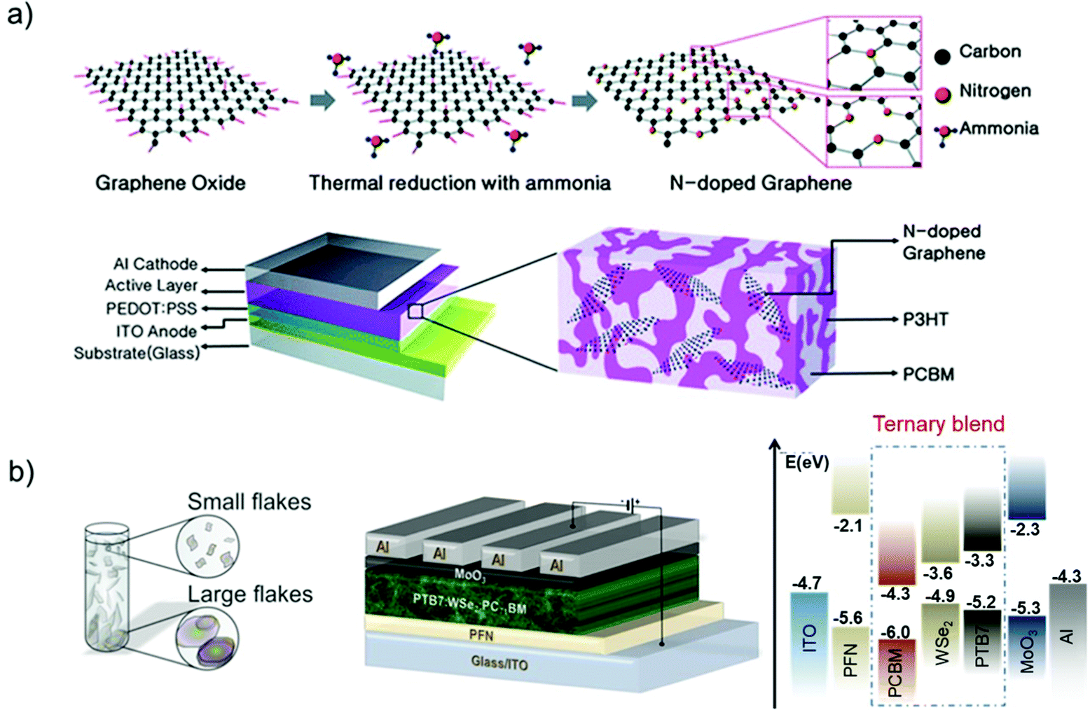 | ||
| Fig. 8 (a) Schematic of the N-doping process of RGO and BHJ OSC using N-doped graphene/P3HT:PC61BM as the active layer. Adapted from ref. 572. (b) Schematic of the WSe2 flake production through LPE, and schematic of the device structure and energy levels. Adapted with permission from ref. 336, Copyright 2017, American Chemical Society. | ||
Similarly, Robaeys et al.574 used solution-processed graphene flakes, produced by the LPE of pristine graphite, as an additive in P3HT:PC61BM-based OSCs. It was shown that graphene addition determines the formation of a continuous active film with an interpenetrating structure by improving the crystallinity of P3HT. Nevertheless, like NRGO, solution-processed graphene flakes cannot be considered as an energy cascade component in a ternary BHJ OSC due to lack of a bandgap and therefore appropriate energy level matching. Contrarily, solution-processed graphene flakes can be considered as an additive to improve the crystallization and morphology of P3HT, beyond the improvement of charge transport properties. Consequently, graphene flakes can favor better balancing between μe and μh compared to the reference cell.
Graphene nanoflakes with controlled lateral size and functionalized with EDNB (EDNB-GNFs) were demonstrated as a ternary compound acting as an efficient electron-cascade acceptor material in air-processed PCDTBT:PC71BM-based OSCs.484 The functionalization process allowed the HOMO and LUMO levels of GNFs to be matched with the HOMO and LUMO levels of the hosting polymer and fullerene components, respectively. Furthermore, EDNB-GNFs acted as a highly conductive bridge between polymer chains and fullerene balls, thus offering two additional interfaces for exciton dissociation, as well as multiple routes for charge transfer at the donor/acceptor interfaces. The as-prepared ternary OSCs achieved an η value of 6.59%, which was ∼18% higher than that of the binary reference (η = 5.59%). The same group investigated the role of GO covalently linked with porphyrin moieties (GO-TPP) into the active layer of PCDTBT:PC71BM and PTB7:PC71BM,575 showing that the addition of GO-TPP induces favorable energy alignment between the energy levels of the donor and acceptor, facilitating the electron-cascade effect. The optimized ternary PTB7-based OSCs, containing 0.3% GO-TPP, exhibited a remarkable η of 8.81%, which was ∼16% higher than the binary reference one.574
Kim et al.576 incorporated GO-QDs in PTB7:PC71BM-based OSCs and investigated the effect of reduction of GO on the PV performance. It was found that the addition of partially reduced GO-QDs (RGO-QDs) in the active layer enhanced the η value from 6.7% up to 7.6% because of the ideal balance between optical absorption and conductivity of QDs.575 Most recently, RGO-Sb2S3 hybrid flakes have been used as additives in PCDTBT:PC71BM-based OSCs.577 Hybrid RGO-Sb2S3 combines the advantages of individual materials in which Sb2S3—acting as a secondary light-harvesting antenna in the visible spectrum—enhances the light absorption of the device, while RGO flakes offer highly conductive multiple charge-transfer percolation paths, suitable for ballistic electron transport to the LUMO of PC71BM.576 Moreover, the RGO sheets accelerate charge transfer, hindering the recombination phenomena in inorganic nanocrystals.576 Therefore, the resulting cells exhibited a significant η of 7%, corresponding to an enhancement of ∼23% compared to the reference device.576 Kim et al. recently reported the utilization of size-selected GO flakes as the third component in PTB7:PC71BM-based OSCs.578 GO nanosheets with lateral sizes ranging from nanometers to micrometers were fabricated by a physical sonication process.577 The physical size of the GO flakes affects the GO dispersion stability and morphological aggregation of the ternary blend.577 In particular, it was found that the use of GO with lateral sizes of 500–750 nm maximizes both hole and electron mobilities of ternary OSCs.577 Consequently, the non-geminate recombination was reduced. The corresponding ternary OSCs reached an η value as high as 9.21% by increasing the FF to 69.4% in inverted devices, while the reference binary OSCs exhibited an η value of 7.94%.577
Other 2D materials have been exploited as additives in OSCs. Bruno et al.579 used WS2 nanotubes in P3HT-QDs devices (which can also be classified as an organic–inorganic hybrid SC; see Section 7) as additives. In situ laser-induced anchoring of noble-metal NPs onto the surface of thin GO, WS2, MoS2, and BN have been developed to design special additives for OSCs.580 In particular, WS2 nanosheet–Au NP assemblies added in PCDTBT:PC71BM allowed the corresponding cells to achieve an ∼13% enhancement in η compared to the binary reference.579 This effect was attributed to the efficient synergy of plasmon-enhanced absorption of Au NPs and superior charge transport into WS2 nanosheets, as well as energy-level matching between the polymer and intermediate WS2 nanosheets.579 WSe2 nanoflakes of different sizes were also used as the third component in ternary PTB7:PC71BM-based OSCs (Fig. 8b).336
Three WSe2 samples, with different average lateral sizes (below 20 nm, between 30 and 50 nm, and above 50 nm) were investigated.336 Upon the introduction of medium-sized flakes, an η value of 9.45% was measured, which is one of highest reported for OSCs based on PTB7 as the polymer donor.336 The observed enhancement was attributed to the synergistic effect of absorption and charge transfer processes.336 Notably, only medium-sized WSe2 flakes contributed to η enhancement.336 This was linked with the similar size of WSe2 flakes and PC71BM domains in the ternary blend.336 Therefore, the insertion of such nanoflakes introduces additional percolation pathways in the photoactive blend, promoting electron extraction and therefore collection.336 These results highlighted the importance to match the morphological properties of 2D materials with the photoactive components of OSC blends.336 Lately, Yang et al. incorporated LPE-produced black phosphorus nanoflakes (BPNFs) with an average size of 46 nm in poly([2,6′-4,8-di(5-ethylhexylthienyl)benzo[1,2-b;3,3-b]dithiophene]{3-fluoro-2[(2-ethylhexyl)carbonyl]thieno[3,4-b]thiophenediyl}):low-bandgap NFA (PTB7-Th:IEICO-4F)-based OSCs as the third component.583 BPNFs were used as the morphology modifier to improve the performance of fullerene-free OSCs.582 The incorporation of BPFNs promotes molecular ordering and higher phase purity of the ternary blend, contributing to lowering the charge transport resistance and suppressing charge recombination compared to the binary blend without BPFNs.582 As a result, ternary OSCs exhibited an η value of 12.2%, whilst the η value of binary OSCs was 11.4%.582 Moreover, the ternary OSC with BPNFs retains 73% of its initial η after thermal treatment at 150 °C in a N2 atmosphere for over 3 h, while the binary OSC retains only 60% of its initial η under the same condition.582 The improvement in stability was ascribed to the retarding of phase mixing in BHJ during the aging period as a consequence of the space confinement effect induced by BPFNs.582
The effect of hydrogenation on MoSe2 nanosheets, used as additives in PTB7-Th:PC71BM OSCs, was also investigated in ternary devices.584 The OSCs exhibited an η value of 10.44%, which represent a 16% increment compared to the reference binary OSCs.583 The obtained results were associated with the establishment of optimized percolation pathways in the active layer.583 Furthermore, the ternary OSC maintained 70% of its initial η value after continuous heating at 100 °C for approximately 1 h.583 The improvement in performance, compared to the reference OSC, was attributed to enhanced exciton generation and dissociation at the MoSe2–fullerene interfaces and balanced μe and μh.583 Very recently, chlorine-functionalized graphdiyne has been successfully applied as a multifunctional solid additive to fine-tune the morphology and improve the efficiency and reproductivity of NFA-based OSCs, which reached an η value of 17.3% (certified η of 17.1%).585
Table 2 summarizes the main results achieved with OSCs using GRMs as the active layer components.
| Material | Usage | Device structure | Cell performance | Ref. | |||
|---|---|---|---|---|---|---|---|
| J SC (mA cm−2) | V OC (V) | FF (−) | η (%) | ||||
| Fullerene-grafted graphene | Electron acceptor | ITO/PEDOT:PSS/P3HT:C60-G/Al | 4.45 | 0.56 | 0.49 | 1.22 | 564 |
| Chemically synthesized GO-ethylene-dinitro-benzoyl (GO-EDNB) | Electron acceptor | ITO/PEDOT:PSS/P3HT:GO-EDNB/Al | 3.32 | 0.72 | 0.4 | 0.96 | 565 |
| Laser produced GO-ethylene-dinitro-benzoyl (LGO-EDNB) | Electron acceptor | ITO/PEDOT:PSS/PCDTBT:LGO-EDNB/TiOx/Al | 5.29 | 1.17 | 0.39 | 2.41 | 566 |
| RGO | Electron acceptor | FTO/TiO2 NR-ZnO NP/RGO/P3HT/PEDOT:PSS/Au | 10.78 | 0.68 | 0.52 | 3.79 | 567 |
| Nitrogen doped graphene (N-RGO) | Additive | ITO/PEDOT:PSS/P3HT:PC61BM:N-RGO/Ca/Al | 14.90 | 0.6 | 0.49 | 4.50 | 572 |
| Graphene flakes | Additive | ITO/PEDOT:PSS/P3HT:PC61BM:graphene/Ca/Al | 8.00 | 0.6 | 0.66 | 3.17 | 573 |
| Functionalized graphene nanoflakes (GNFs) | Additive | ITO/PEDOT:PSS/PCDTBT:PC71BM:GNF-EDNB60/TiOx/Al | 12.56 | 0.89 | 0.57 | 6.41 | 484 |
| Graphene-based porphyrin molecule (GO-TPP) | Additive | ITO/PEDOT:PSS/PTB7:PC71BM:GO-TPP/TiOx/Al | 17.98 | 0.77 | 0.61 | 8.58 | 574 |
| Graphene oxide quantum dots (GOQDs) | Additive | ITO/PEDOT:PSS/PTB7:PC71BM:GOQD/TiOx/Al | 15.20 | 0.74 | 0.68 | 7.60 | 575 |
| RGO-antimony sulfide (RGO-Sb2S3) hybrid nanosheets | Additive | ITO/PEDOT:PSS/PCDTBT:PC71BM:RGO-Sb2S3/TiOx/Al | 13.47 | 0.92 | 0.55 | 6.81 | 576 |
| Medium sized GO | Additive | ITO/ZnO/PTB7:PC71BM:MGO/MoO3/Al | 18.00 | 0.74 | 0.69 | 9.09 | 577 |
| WS2 decorated with Au NPs | Additive | ITO/PEDOT:PSS/PCDTBT:PC71BM:PCDTBT:WS2-Au/TiOx/Al | 12.3 | 0.89 | 0.58 | 6.30 | 579 |
| WSe2 | Additive | ITO/PFN/PTB7-WSe2-PC71BM/MoO3/Al | 17.84 | 0.73 | 0.72 | 9.45 | 336 |
| BPFNs | Additive | ITO/ZnO/PTB7-Th:IEICO-4F:BPNFs/MoO3/Ag | 23.44 | 0.71 | 0.73 | 12.20 | 582 |
| Hydrogen plasma–treated MoSe2 | Additive | ITO/ZnO/PTB7-TH:PC71BM/MoO3/Al | 18.69 | 0.78 | 0.70 | 10.2 | 583 |
| Chlorine-functionalized graphdiyne | Additive | ITO/PEDOT:PSS/PM6:Y6/PFN-Br/Al | 26.09 | 0.84 | 0.79 | 17.32 | 584 |
| Zn–porphyrin based metal–organic framework nanosheets (Zn2(ZnTCPP)) | Additive | ITO/PEDOT:PSS/P3HT:PC61BM: Zn2(ZnTCPP):BCP:Al | 10.80 | 0.69 | 0.69 | 5.2 | 581 |
| Bi2OS2 nanosheets | Additive | ITO/ZnO/ITIC:Bi2OS2:PBDB-T/MoO3/Ag | 18.61 | 0.94 | 0.71 | 12.31 | 582 |
| g-C3N4 QDs | Additive | ITO/ZnO/g-C3N4:P3HT:PC61BM/PEDOT:PSS/Ag | 11.44 | 0.61 | 0.60 | 4.23 | 278 |
| ITO/ZnO/g-C3N4:PBDTTT-C: PC71BM/PEDOT:PSS/Ag | 15.9 | 0.70 | 0.57 | 6.62 | |||
| ITO/ZnO/g-C3N4:PTB7-Th:PC71BM/PEDOT:PSS/Ag | 16.74 | 0.78 | 0.70 | 9.2 | |||
4.3 CTLs
The most successful application of GRMs for OSCs is in CTLs as either ETLs or HTLs. To design high-efficiency OSCs, ETL/HTL are positioned between the photoactive layer and anode/cathode, to reduce the potential barriers at both the interfaces and suppress the current leakage and/or charge recombination.586 Preferably, to ensure ohmic contacts at both interfaces, the ϕW value of an ETL should match the LUMO level of the acceptor, while the ϕW value of the HTL should match the HOMO level of the donor.587A large number of HTL materials for OSCs have been investigated, including transition metal oxides (e.g., V2O5, NiOx)588,589 and self-assembled organic molecules, e.g., poly(3,4-ethylenedioxythiophene) polystyrene sulfonate (PEDOT:PSS).590,591 With regard to ETLs, the most efficient materials currently used are n-type inorganic (e.g., TiOx and ZnO)592 and organic semiconductors.593 However, there are several issues related to the most established CTLs. In particular, the main issues are related to the strong acidic and hygroscopic character of PEDOT:PSS and the sensitiveness of sol–gel-prepared TiOx to moisture. Therefore, costly manufacturing in a controlled atmosphere is often required.594 In addition, charge transporting materials do not always allow ϕW tuning and/or solution processability.595 In this context, graphene derivatives596 and other 2D materials597 have been extensively investigated as buffer layers in order to fully exploit their features, including solution processability, low-cost fabrication, environmental stability, and ϕW tunability via functionalization methods.
 | ||
| Fig. 9 (a) Chemical structures of the PTB7 donor polymer, PC71BM acceptor, and GO HTL. Schematic of a standard OSC indicating the location of CTLs. Comparative PV performance of PTB7:PC71BM-based OSC with PEDOT:PSS or GO HTLs. Adapted with permission from ref. 609, Copyright 2011, American Chemical Society. (b) Schematic of the OSC structure. I–V curves of OSCs based on different HTLs. Adapted from ref. 616. (c) Schematic of the inverted-type OSC incorporating a MoS2 HTL. Schematic of the structure of the thin-layer MoS2 buffer layer (side view) and schematic of the monolayer flake of MoS2 along the 0001 direction (top view). Adapted from ref. 620. | ||
An alternative way to increase the electrical conductivity of GO relies on its mixing with SWCNTs.613 This approach allowed P3HT:PC61BM-based OSCs to reach an η value of 4.1%.612 Furthermore, surfactant-free Au NPs were incorporated between the photoactive layers and GO HTL, leading to an η value increase of ∼30% compared to the PEDOT:PSS-based reference.614 In addition, the GO-based devices retained 50% of their initial η after 45 h of continuous illumination, while the reference devices based on PEDOT:PSS completely degraded after 20 h.613 The η enhancement was attributed to an increase in the exciton generation rate caused by Au NP-induced plasmon absorption enhancement. Meanwhile, the stability performance was ascribed to the suppression, in presence of GO, of oxygen and/or In diffusion from ITO toward the P3HT:PC61BM.613
Li et al.615 investigated deposited GQDs as the HTL material in DR3TBDT:PC71BM- and P3HT:PC61BM-based OSCs (DR3TBDT is a small-molecule donor based on the benzo[1,2-b:4,5-b′]dithiophene unit).616 GQD films exhibited homogenous morphology and high conductivity, yielding P3HT:PC61BM-based OSCs with an η value of 3.51%.615 This value was similar to that measured for PEDOT:PSS-based OSCs (η = 3.52%).615 In addition, GQD-based OSCs exhibited longer lifetime and more reproducible η compared to the reference device.615
An effective approach to enhance the performance of GO-based HTLs is to tune their ϕW through functionalization routes.112 In ref. 617, a fluorinated RGO (FRGO) was synthetized with a ϕW value of 4.9 eV using a F-containing phenylhydrazine-based reductant. The as-produced FRGO was then used as the HTL in PTB7:PC71BM- and P3HT:ICBA-based OSCs (Fig. 9b).616 The functionalization process detached oxygen functional groups from GO flakes, while concomitantly doping the edges and basal planes of the flakes themselves with F.616 Due to the ϕW increase, the FRGO-based OSCs exhibited similar performance and higher stability compared to those of the PEDOT:PSS-based reference.616 A series of GOs with tuned oxidation (pr-GO) were synthetized by Li et al.618 strictly by controlling the preoxidation steps, oxidation time, and oxidant content, leading to ϕW values between 4.74 and 5.06 eV. By precisely controlling the oxidation time, a P3HT:PC61BM-based OSC using pr-GO HTL reached an η value of 3.74%, which was ∼3.60% higher than that reported for the PEDOT:PSS-based reference.617 Stratakis et al.619 demonstrated that GO ϕW can be effectively tuned by UV laser irradiation in the presence of Cl gas. In particular, by irradiating ultrathin GO films with a pulsed laser in the presence of a dopant Cl precursor gas, a simultaneous reduction and Cl doping of GO lattice was achieved.618 Following the irradiation process, Cl atoms were linked to both basal planes and edges of GO. The ϕW value of GO was tuned by controlling the laser exposure time.618 In particular, the ϕW value of chlorinated GO (GO-Cl) was adjusted from 4.9 eV in GO to a maximum of 5.23 eV in GO-Cl by increasing the laser exposure level up to 60 laser pulses (pulse duration = 20 ns; wavelength = 248 nm; power of 50 mW; beam profile = 20 × 10 mm2).618 The induced polar character of C–Cl bonds is responsible for the downward shift in EF in the VB of GO-Cl and the subsequent increase in ϕW compared to pristine GO.618 This ϕW tuning determined the energy matching between GO-Cl and the PCDTBT donor, allowing the resulting OSC to reach an η value higher than that of PEDOT:PSS-based reference.618 Phosphorylated GO was recently used as HTL in PTB7:PC71BM-, PBDTTT-C:PC71BM-, and P3HT:PC61BM-based OSCs, enhancing their η from 6.28%, 5.07%, and 2.78% (in pristine GO-based devices) to 7.90%, 6.59%, and 3.85%, respectively.620 The proposed phosphate ester modification increased the GO film roughness and hydrophobicity, while the p-doping of the GO increased ϕW from 4.24 to 4.70 eV, providing better matching with the HOMO level of the polymer donor.619
In addition to graphene-based materials, solution-processed TMDs have also been widely investigated as HTL materials. For example, Gu et al.621 exploited a film of MoS2 flakes, produced by the chemical Li intercalation method, as the HTL in P3HT:PC61BM- and PTB7:PC71BM-based OSCs. The resulting MoS2-based OSCs achieved η values of 4.02% and 8.11% for P3HT:PC61BM and PTB7:PC71BM active layers, respectively (Fig. 9c).620 These η values were higher than those measured for the reference OSCs using thermally evaporated MoO3 HTLs.620
The superior HTL performance of MoS2 compared to that of vacuum-evaporated MoO3 was attributed to the inferior trap density compared to the MoO3 reference, providing higher hole concentration at VOC (i.e., ∼1016 cm−3 in MoS2vs. ∼1016 cm−3 in MoO3).620 In addition, at the MoS2/P3HT interface, the presence of a surface dipole with the negative charge end pointing toward the active film electrode and positive charge end pointing toward the Ag electrode reinforces the actual built-in potential across the device, suppressing charge recombination and leading to a more effective charge extraction capability.620 Likewise, Yun et al. prepared a p-type MoS2 (p-MoS2) layer by HAuCl4·3H2O doping.622 This process increased the MoS2ϕW value from 4.52 to 4.76 eV.621 As a result, P3HT:PC61BM-based OSCs using p-MoS2 HTL exhibited an η value of 3.4%, which was higher than that of pristine MoS2-based OSCs (η = 2.8%), owing to the better energy-level matching between the P3HT HOMO level and HTL ϕW.621 In the research activity of energy-level optimization of HTL, Le et al. further increased the ϕW value of MoS2 up to 4.9 eV by UV/ozone (UVO) treatment, providing excellent matching with the HOMO level of P3HT (∼5 eV).623 The resulting MoS2-based OSCs achieved an η value of 2.44%, which was similar to that of the PEDOT:PSS-based reference (η = 2.81%).622 Moreover, the use of MoS2 HTL extended the device stability in air by protecting the ITO surface from the hygroscopic nature of PEDOT:PSS.622 An increase in MoS2ϕW was also achieved by introducing O atoms inside the lattice of MoS2 flakes (O-MoS2) via UVO post-treatment.624 The optimized O-MoS2 flakes were used as HTLs in PTB7:PC71BM-based OSCs, which displayed an η value of 7.64%—53% higher than that of the cell using pristine MoS2 and comparable to that obtained using PEDOT:PSS (7.6%).623 In addition, the Rs value of the device with O-MoS2 was considerably lower (1.88 Ω □−1) than that obtained using MoS2 (4.03 Ω □−1).623 The incorporation of O atoms into the MoS2 lattice can act as a type of doping or alloy, reducing structural defects by the filling of vacancies, as well as increasing ϕW (up to 4.93 eV) to match the HOMO level of P3HT.623 Liu et al. proposed a further surface modification pathway of MoS2 with a hydrophilic surfactant via electrostatic interaction.625 Subsequently, they fabricated PTB7:PC71BM-based OSCs with a modified MoS2 HTL, achieving η > 7%.624 Yang et al. decorated MoS2 flakes with Au NPs in order to create localized surface plasmon resonance effects to boost η.626 In fact, Au NPs act as plasmonic near-field antennas,627,628 increasing the absorption cross-section of the photoactive layer.625 As a result, PTB7:PC71BM-based OSCs using the MoS2-Au hybrid as the HTL, exhibited an η value of 7.25%, which represents a 17.3% increase compared to that of pristine MoS2 HTL-based devices (η = 6.18%).625 Zheng et al. proposed a graphene–MoS2 heterostructure (GMo) as an interlayer between the ITO and PEDOT:PSS HTL in OSCs based on a binary PTB7-Th:PC71BM system.629 GMo was hydrothermally synthesized using thiourea/glycerol, LPE-produced graphene, and phosphomolybdic acid as the precursors.628 The few layers of oxygen-incorporated MoS2 contained both 2H and 1T phases.628 GMo-based OSCs reached η = 9.5%, while retaining more than 93% of the initial η over 1000 h.628 Beyond MoS2, other TMDs have been investigated as HTLs. Kwon et al. used WS2 treated with UVO as the HTL in P3HT:PC61BM-based OSCs.630 The UVO treatment modified the ϕW value of WS2 from 4.75 to 4.95 eV, improving the alignment with the LUMO level of P3HT in addition to the removal of surface contaminants.629 The combination of these effects allowed the achievement of η = 3.08% (comparable to that of the PEDOT:PSS-based reference (3.23%)).629 UVO treatment was also used for TaS2 nanosheets, used both as the HTL and ETL in P3HT:PC61BM-based OSCs.631 The ϕW value of TaS2 changed from 4.4 eV to 5.1 eV and η = ∼3.06% could be achieved. This value was similar to that measured for the PEDOT:PPS-based OSCs as the reference (3.28%).629 Gu et al. introduced NbSe2 HTL in inverted PTB7:PC71BM- and P3HT:PC61BM-based OSCs, reaching η of ∼8.10% and ∼3.05%, respectively.632 These η values were higher than those of OSCs based on vacuum-deposited MoO3 (7.54%) and spin-coated PEDOT:PSS (2.7%).631
The enhancement of η was attributed to the flake-like 2D structure, which exhibits a lower trap density, as well as to the existence of surface dipoles, which promote charge extraction processes. Lastly, layered bismuth selenide nanoplatelets (L-Bi2Se3) were implemented as the HTL in inverted P3HT:PC61BM-based OSCs.633 The corresponding OSCs reached η = 4.37%, which was higher than the η value of OSCs based on evaporated MoO3 HTL (3.91%).632 The η improvement was ascribed to the high conductivity of L-Bi2Se3.632 Moreover, the L-Bi2Se3ϕW was found to increase with aging under the ambient conditions due to O-induced p-doping, resulting in improved VOC and FF.632 More recently, Li et al. demonstrated the use of LPE-produced few-layer WS2 and MoS2 nanosheets as the HTL materials for high-efficiency NFA-based OSCs (Fig. 10).634 The cells used Y6471 or IT-4F635 as small-molecule NFAs and PBDB-T-SF636 or PBDB-T-2F634 as the polymer donors. Binary PBDB-T-SF:IT-4F and ternary PBDB-T-2F:Y6:PC71BM OSCs based on WS2 as the HTL exhibited an η value of 15.8% and 17.0%, respectively, which were higher than the corresponding reference OSCs based on PEDOT:PSS, i.e., η of 13.5% and 16.4%, respectively.633 The observed performance enhancement was attributed to a reduction in bimolecular recombination losses (i.e., losses determined by the recombination of an electron with a hole, thus directly depending on both electron and hole concentrations) compared to PEDOT:PSS-based OSCs.633 The lower bimolecular recombination in WS2-based devices compared to MoS2 and PEDOT:PSS devices was ascribed to the deeper ϕW value of WS2 on ITO (i.e., 5.5 eV vs. 5.4 eV and 4.8 eV for MoS2 and PEDOT:PSS on ITO, respectively).633 The optimal WS2ϕW allowed charge collection to be improved and surface energy to be reduced, leading to quasi-ideal phase separation.633
 | ||
| Fig. 10 (a) Chemical structure of PBDB-T-2F, Y6, and PC71BM and the corresponding LUMO and HOMO energies. (b) Schematic of the standard OSC architectures employed. (c) J–V curves of OSCs based on PBDB-T-2F:Y6 and PBDB-T-2F:Y6:PC71BM with different HTLs. (d) EQE curves of OSCs based on a PBDB-T-2F:Y6:PC71BM active layer for different HTLs. (e) A comparison of the performances of previously reported OSCs with 2D material interfaces. Adapted from ref. 633. | ||
Table 3 summarizes the main results achieved with OSCs using HTLs based on GRMs.
| Material | Usage | Device structure | Cell performance | Ref. | |||
|---|---|---|---|---|---|---|---|
| J SC (mA cm−2) | V OC (V) | FF (−) | η (%) | ||||
| GO | HTL | ITO/ZnO/PTh4FBT:PC71BM/VOx/GO/Ag | 13.2 | 0.76 | 0.67 | 6.7 | 606 |
| Partial reduced GO | HTL | ITO/pr-GO/PCDTBT-PC71BM/TiOx/Al | 11.18 | 0.89 | 0.59 | 5.96 | 607 |
| UV-O3 treated GO | HTL | ITO/UV-O3 treated GO/PTB7:PC71BM/LiF/Al | 15.21 | 0.72 | 0.68 | 7.39 | 609 |
| Sulfonic acid-functionalized RGO | HTL | ITO/sr-GO/PTB7:PC71BM/Ca/Al | 15.3 | 0.75 | 0.63 | 7.18 | 610 |
| GO-SWCNT | HTL | ITO/GO-SWCNT/P3HT:PC61BM/Ca/Al | 10.82 | 0.6 | 0.63 | 4.1 | 612 |
| GQDs | HTL | ITO/GO/P3HT:PC61BM/Ca/Al | 10.20 | 0.52 | 0.66 | 3.51 | 614 |
| Fluorine-functionalized RGO | HTL | ITO/FRGO/P3HT:PC61BM/Ca/Al | 8.78 | 0.6 | 0.7 | 3.64 | 616 |
| Partial oxidized GO (pr-GO) | HTL | ITO/pr-GO/P3HT:PC61BM/LiF/Al | 10.40 | 0.61 | 0.59 | 3.74 | 617 |
| Photochlorinated GO (GO-Cl) | HTL | ITO/GO-Cl/PCDTBT:PC71BM/TiOx/Al | 13.65 | 0.88 | 0.55 | 6.56 | 618 |
| Phosphorylated GO | HTL | ITO/P-GO/PTB7:PC71BM/Ca/Al | 16.12 | 0.71 | 0.68 | 7.9 | 619 |
| MoS2 | HTL | ITO/ZnO/PTB7:PC71BM/MoS2/Ag | 15.9 | 0.72 | 0.71 | 8.11 | 620 |
| p-Doped MoS2 | HTL | ITO/p-doped MoS2/P3HT:PC61BM/Ca/Al | 8.62 | 0.59 | 0.66 | 3.38 | 621 |
| UV/ozone-treated MoS2 (UVO MoS2) | HTL | ITO/UVO MoS2/P3HT:PC61BM/LiF/Al | 7.97 | 0.52 | 0.68 | 2.81 | 622 |
| Oxygen-incorporated chemical exfoliated MoS2 (O-ceMoS2) | HTL | ITO/O-ceMoS2/PTB7:PC71BM/PFN/Al | 14.98 | 0.73 | 0.7 | 7.64 | 623 |
| Modified ce-MoS2 (m-MoS2) | HTL | ITO/m-MoS2/PTB7:PC71BM/PFN/Al | 14.71 | 0.73 | 0.67 | 7.26 | 624 |
| MoS2 decorated with Au NPs (MoS2@Au) | HTL | ITO/MoS2@Au/PTB7:PC71BM/PFN/Al | 15.44 | 0.72 | 0.65 | 7.25 | 625 |
| Graphene-MoS2/PEDOT:PSS | HTL | ITO/Graphene-MoS2/PEDOT:PSS/PTB7-Th:PC71BM/Ca/Ag | 17.2 | 0.77 | 0.72 | 9.4 | 628 |
| UV-O3 treated MoS2 | HTL | ITO/UV-O3 treated MoS2/P3HT:PC61BM/LiF/Al | 7.81 | 0.6 | 0.63 | 2.96 | 629 |
| UV-O3 treated WS2 | HTL | ITO/UV-O3 treated WS2/P3HT:PC61BM/LiF/Al | 7.87 | 0.61 | 0.64 | 3.08 | 629 |
| UV-O3 treated TaS2 | HTL | ITO/TaS2/P3HT:PC61BM/LiF/Al | 7.87 | 0.61 | 0.64 | 3.06 | 630 |
| NbSe2 nanosheets | HTL | ITO/ZnO/PTB7:PC71BM/NbSe2/Ag | 16.04 | 0.72 | 0.7 | 8.1 | 631 |
| Layered bismuth selenide (L-Bi2Se3) nanoplates | HTL | ITO/ZnO/P3HT:PC61BM/L-Bi2Se3/Ag | 9.91 | 0.65 | 0.68 | 4.37 | 632 |
| WS2 | HTL | ITO/WS2/PBDB-T-SF:IT-4F/PFN-Br/Al | 20.6 | 0.88 | 0.74 | 13.5 | 633 |
| WS2 | HTL | ITO/WS2/PBDB-T-2F: Y6: PC71BM/PFN-Br/Al | 26 | 0.84 | 0.78 | 17 | 633 |
| UV treated Ti3C2Tx | HTL | ITO/UV-MXene/PBDB-T:ITIC/Ca/Al | 15.98 | 0.89 | 0.64 | 9.02 | 651 |
| GO | HTL | ITO/GO/P3HT:PC61BM/GOCs/Al | 10.30 | 0.61 | 0.59 | 3.67 | 636 |
| GO-Cl | HTL | ITO/GO-Cl/PTB7:PC71BM/GO-Li/TiOx/Al | 19.59 | 0.76 | 0.62 | 9.14 | 650 |
| PEDOT:PPS-GO | HTL | ITO/PEDOT:PSS-GO/PM6:Y6/PDINO–G/Al | 25.65 | 0.85 | 0.76 | 16.5 | 652 |
| PEDOT:PSS:GO | HTL | ITO/PEDOT:PSS/SPGO/PTB7:PC71BM/Al | 17.3 | 0.67 | 0.41 | 4.82 | 640 |
| g-C3N4-doped PEDOT:PSS | HTL | ITO/g-C3N4-doped PEDOT:PSS/PM6:Y6/PFN-Br/Ag | 26.71 | 0.84 | 0.73 | 16.38 | 641 |
| α-In2Se3 nanosheets | HTL | ITO/α-In2Se3/PBDB-T:ITIC/Ca/Al | 16.69 | 0.88 | 0.65 | 9.58 | 642 |
| WS2 nanosheets | HTL | ITO/WS2/PBDB-T-2F:Y6:PC71BM/PFN-Br/Ag | 26.0 | 0.83 | 0.72 | 15.6 | 643 |
| MoS2 nanosheets | HTL | ITO/WS2/PBDB-T-2F:Y6:PC71BM/PFN-Br/Ag | 25.3 | 0.81 | 0.71 | 14.9 | 642 |
Similar Cs2CO3-based functionalization was applied to GQDs (GQDs-Cs2CO3), which were then used as the ETL in inverted P3HT:PC61BM-based OSCs.638 The OSCs exhibited an η value of 3.23%, which was 56% higher than that of OSCs using pristine Cs2CO3 HTL.637 In addition, while GQDs-Cs2CO3-based devices retained 50% of their original η under ambient conditions (exposition for 1200 h), the η value of pristine Cs2CO3-based device decreased to 17% of its initial value.637 The high η and stability of GQDs-Cs2CO3-based OSCs were attributed to both optimal electron extraction and suppression of leakage current, as well as the immobilization of Cs+ ions on GQDs in the HTL, delaying their diffusion into the P3HT.637 Meanwhile, n-doped GO was produced through chemical Li intercalation, leading to functionalized GO-Li with ϕW of 4.3 eV.639
The low ϕW value of GO-Li was ascribed to the presence of Li atoms with low electronegativity.638 In detail, Li atoms bonded to GO release their valence electrons to GO, leading to the formation of an electric dipole induced by Li+.638 The charge transfer from Li to GO plane shifts the Fermi level toward the vacuum, inducing a difference between the Fermi level of the two materials of 0.67 eV, explaining the decrease of ϕW.638 In PCDTBT:PC71BM-based OSCs, the GO-Li layer, which is inserted between TiOx and photoactive blend, acts as an interfacial engineering material, increasing η up to 6.29% (4.89% in GO-based OSCs and 5.51% in interlayer-free OSCs).638 These results prove the bifunctional role of GO-Li acting as (1) an interfacial engineering material that improves the ohmic contact between the cathode and the ETL, while increasing the internal electric field amplitude;638 (2) a protection layer against humidity and oxygen, enhancing the device stability during prolonged illumination.638
Beyond the intercalation of alkali metals in GO, an alternative n-doping strategy of RGO was developed by producing RGO-ZnO and RGO-TiO2 nanocomposites, which were then used as the ETL in inverted PTB7:PC71BM-based OSCs.644 The RGO-ZnO- and RGO-TiO2-based OSCs achieved η values of 7.50% and 7.46%, respectively.643 These values were comparable to those obtained using pristine ZnO (7.39%) and TiO2 (7.22%).643 The authors also compared their RGO-metal oxide (MO)-based OSCs with devices containing thermally evaporated bathocuproine (or 2,9-dimethyl-4,7-diphenyl-1,10-phenanthroline) (BCP) as ETLs, obtaining fairly comparable η (7.47%) due to the capability of RGO to balance hole and electron mobilities of the devices.643 Subsequently, RGO-MO ETLs were also exploited in PCDTBT:PC71BM-based,645 P3HT:PC61BM-based,646 and low-bandgap quinoxaline-based D-A copolymer:PCBM-based647 OSCs.
A RGO-PC61BM composite was produced by Qu et al. by anchoring PC61BM onto GO through a pyridine moiety to be used as the ETL in P3HT:PC61BM-based OSCs.648 The RGO-PC61BM nanocomposite exhibits higher solubility compared to RGO and a low ϕW value of 4.4 eV, which matched the LUMO level of the electron acceptor.647 Therefore, the modified PC61BM OSCs significantly improved the η value (3.89%) compared to OSCs using pristine RGO or pyrene-PC61BM ETLs.647
Hu et al. used GQDs functionalized with ammonium iodide at the edge as a thickness-insensitive ETL with high optical transparency.649 PCDTBT:PC71BM-based OSCs using functionalized GQDs exhibited an η value of 7.49%, which was significantly higher than that of the reference cells using calcium as the ETL.648 Importantly, the performance of OSCs was insensitive to the thickness of the GQD layer (i.e., 2–22 m).648
Solution-processed BP flakes in ethanol were also recently demonstrated as an effective interfacial layer between the ZnO ETL and PTB7:PC71BM active layer in inverted OSCs.650 The addition of the BP interlayer enhanced the η value by 11%, reaching the maximum value of 8.25%.649 The improvement of η was attributed to the formation of a cascaded band structure between PC71BM, ZnO, and BP flakes, which facilitates the electron transport and suppresses the carrier recombination near the cathode.649 Furthermore, the BP-incorporated OSC has shown superior air stability, exhibiting a degradation of 5.82% after two days, compared to the reference device, which exhibited a degradation of 9.29% in the same timeframe.649 Konios et al. demonstrated the simultaneous use of ϕW-tuned functionalized GO derivatives as both HTL and ETL in PCDTBT:PC71BM- and PTB7:PC71BM-based OSCs.651 The ϕW tuning of GO took place by either photochlorination618 or Li neutralization638 for ϕW increase or decrease, respectively. Consequently, it was possible to match the GO-Cl ϕW with the HOMO level of both PCDTBT and PTB7 donor, as well as GO-Li ϕW with the fullerene LUMO level, enabling the balance between μe and μh.650 As a result, both graphene-based OSCs significantly outperformed the reference ones, leading to η improvement of 30% and 19% for PCDTBT- and PTB7-based devices, respectively.650 In particular, the champion device exhibited an η value of 9.14%, which was a record-high value for OSCs using a graphene-based buffer layer.650 In the same context, Yu et al. demonstrated the use of ϕW-tuned MXenes, particularly Ti3C2Tx, as both HTL and ETL in NFA-based OSCs using PBDB-T:ITIC as the active layer.652 The ϕW tuning took place through UVO or hydrazine treatments for ϕW increase and decrease, respectively.651 Therefore, the ϕW value was tuned in the 4.08–4.95 eV range.651 The ϕW modification mechanism was ascribed to the oxidation or reduction of the C element of Ti3C2Tx by UVO or N2H4, respectively.651 The UVO-and N2H4-treated MXenes were used as the HTLs in conventional OSCs and as the ETL in inverted OSCs, respectively.651 The resulting cells exhibited an η value of 9.02% or 9.06% respectively, both comparable to the performance achieved with PEDOT:PSS-based references.651 Pan et al. developed an n-doped graphene ETL for OSCs by adding micromechanically exfoliated single-layer graphene to (N,N-dimethyl-ammonium N-oxide)propyl perylene diimide (PDINO).653 The conductivity of graphene was increased by n-doping with the nitroxide radical of N-oxide in PDINO.652 The resultant n-doped graphene (PDINO-G) possessed increased conductivity, lower ϕW, reduced charge recombination, and increased charge extraction rate compared to pristine PDINO.652 The OSCs based on PTQ10:IDIC-2F with PDINO–G as the ETL exhibited an η value of 13.01%, which was superior to that achieved by OSCs without graphene.652 Furthermore, PM6:Y6-based OSCs using PEDOT:PPS-GO as the HTL and PDINO–G as the ETL displayed an η value as high as 16.52%, significantly higher than that for OSCs without GO and graphene (15.1%).652 The observed performance enhancement was attributed to the higher (by two orders of magnitude) conductivity of graphene-based ETL compared to that of graphene-free ETL, suitable ϕW, and optimal charge extraction.652
More recently, Lee et al. used MoS2 nanoflakes, with an average diameter of 27 nm, as an effective electron transporting interlayer between polyethylenimine ethoxylated (PEIE) and the photoactive layer in OSCs.654
MoS2 nanoflakes acted not only as an ETL but also as a sub-photosensitizer (i.e., additional light-absorbing layer), enhancing η by 27%, 11%, and 15% compared to P3HT:PC60BM-, PTB7:PC71BM-, and PTB7-Th:PC71BM-based reference cells, respectively.653 The observed performance enhancement was attributed to effective electron transport via MoS2 nanoflakes supported by an increased Förster resonance energy transfer375,655,656 efficiency of 67% from PTB7:PC71BM to MoS2 nanoflakes.653
Table 4 summarizes the main results achieved with OSCs using ETLs based on GRMs.
| Material | Usage | Device structure | Cell performance | Ref. | |||
|---|---|---|---|---|---|---|---|
| J SC (mA cm−2) | V OC (V) | FF (−) | η (%) | ||||
| GO & Cs-neutralized GO (GOCs) | ETL | ITO/GO/P3HT:PC61BM/GOCs/Al | 10.30 | 0.61 | 0.59 | 3.67 | 650 |
| Cs2CO3 functionalized GQDs-Cs2CO3) | ETL | ITO/GQDs-Cs2CO3/P3HT:PC61BM/V2O5/Au | 9.18 | 0.58 | 0.61 | 3.23 | 637 |
| Lithium-neutralized GO (GO-Li) | ETL | ITO/PEDOT:PSS/PCDTBT:PC71BM/GO-Li/TiOx/Al | 12.51 | 0.89 | 0.57 | 6.29 | 638 |
| ZnO-RGO hybrids | ETL | ITO/PEDOT:PSS/PTB7:PC71BM/ZnO-RGO/Al | 15.19 | 0.72 | 0.69 | 7.5 | 643 |
| TiO2-RGO hybrids | ETL | ITO/PEDOT:PSS/PTB7:PC71BM/TiO2-RGO/Al | 14.99 | 0.74 | 0.67 | 7.46 | 643 |
| TiOx:RGO composites | ETL | ITO/rGO:TiOx/P3HT:PC61BM/MoO3/Ag | 9.85 | 0.64 | 0.61 | 3.82 | 646 |
| RGO-pyrene-PC61BM | ETL | ITO/PEDOT:PSS/P3HT:PC61BM/RGO-pyrene-PC61BM/Al | 9.78 | 0.64 | 0.62 | 3.89 | 647 |
| GQDs functionalized with ammonium iodide (GQD-NI) | ETL | ITO/PEDOT:PSS/PCDTBT:PC71BM/GQD-NI/Al | 10.98 | 0.93 | 0.73 | 7.49 | 648 |
| n-Doped MoS2 | ETL | ITO/n-doped MoS2/P3HT:PC61BM/PEDOT:PSS/Ag | 8.16 | 0.59 | 0.55 | 2.73 | 621 |
| Black phosphorus (BP) | ETL | ITO/ZnO/BP/PTB7:PC71BM/MoO3/Ag | 18.78 | 0.72 | 0.61 | 8.25 | 649 |
| N2H4 treated Ti3C2Tx | ETL | ITO/N2H4-Ti3C2Tx/PBDB-T:ITIC/MoO3/Al | 17.36 | 0.87 | 0.6 | 9.06 | 651 |
| Small sized MoS2 | ETL | ITO/PEIE/MoS2/PTB7-Th:PC71BM/MoO3/Ag | 17.02 | 0.8 | 0.66 | 9.08 | 653 |
| GO-Li | ETL | ITO/GO-Cl/PTB7:PC71BM/GO-Li/TiOx/Al | 19.59 | 0.76 | 0.62 | 9.14 | 650 |
| PDINO-G | ETL | ITO/PEDOT:PSS-GO/PM6:Y6/PDINO–G/Al | 25.65 | 0.85 | 0.76 | 16.5 | 652 |
An ICL collects electron and holes from the respective sub-cells, acting as a recombination site between them.658,659 Therefore, ICL is a critical component in tandem architectures. In addition, an optimal ICL should be uniform, transparent, highly conductive, and resistant to solvents.660 So far, PEDOT:PSS/TiO2,661 PEDOT:PSS:ZnO,662 and LiF/Al/Au/PEDOT:PSS663 have been the most established ICLs, despite the well-known drawbacks attributable to the acidic and aqueous nature of PEDOT:PSS, which have a huge impact on OSC stability.664 In the development of ICL, GRMs have been used both to improve the stability of PEDOT:PSS and in combination with other materials as an alternative to PEDOT:PSS.
Tung et al. used GO:PEDOT:PSS nanocomposite as the ICL in a tandem OSCs consisting of two identical P3HT:PC61BM-based sub-cells.665 The tandem OSCs were fabricated by a direct adhesive lamination process enabled by the sticky GO:PEDOT film.664 An η value of 4.14 and VOC of 0.94 V (∼84% of the sum of the VOC of the two sub-cells) were reported.664 Surprisingly, the presence of GO in the composite increased the PEDOT:PSS electrical conductivity by altering its chain conformation and morphology. Moreover, GO increased the PEDOT:PSS dispersion viscosity, leading to a beneficial effect on the adhesion properties.664 Overall, the addition of GO effectively improved charge extraction at the interface between the HTL and active layer.664
Yusoff et al. incorporated a GO/TiO2 recombination layer into a tandem OSC.491 The overall VOC (1.62 V) was approximately the sum of those of the individual sub-cells (0.94 V and 0.68 V).491 This result indicated that the incorporation of GO in traditional recombination layers can allow the realization of ideal resistance-free interconnection between the front and rear cell, while preserving the optical transparency of the same recombination layers (e.g., TiO2).491 Notably, all the tandem OSCs were solution-processed and stable.491 Finally, Cs-functionalized GO was used in GO-Cs/Al/GO/MoO3 ICL between two PCDTBT-based sub-cells.666 The ICL based on GO promoted recombination between the electrons and holes generated from the front and rear cells, owing to the energy-level matching of the interfaced materials.665 In fact, after MoO3 modification, the ϕW value of GO increased up to 5.3 eV, matching the HOMO level of PCDTBT, while that of Al-modified GO-Cs decreased to 4 eV, matching the LUMO level of PCBM.665 The resulting η and VOC values were 3.91% and 1.69 V, respectively.665 The VOC was almost equal to the sum of the two sub-cells, proving the beneficial role of GRM-based ICLs.665
Table 5 summarizes the main results achieved with tandem OSCs using ICLs based on GRMs.
| Material | Usage | Device structure | Cell performance | Ref. | |||
|---|---|---|---|---|---|---|---|
| J SC (mA cm−2) | V OC (V) | FF (−) | η (%) | ||||
| GO:PEDOT:PSS composite | ICL | Glass/ITO/PEDOT:PSS/P3HT:PC61BM/ZnO/GO:PEDOT:PSS/P3HT:PC61BM/Ca/Al | 7.2 | 1 | 0.58 | 4.14 | 490 |
| GO | ICL | Glass/ITO/GO/PSEHTT:ICBA/TiO2/GO/PSBTBT:PC71BM/ZnO/Al | 8.23 | 1.62 | 0.63 | 8.4 | 491 |
| Cesium neutralized GO (GO-Cs) & GO | ICL | Glass/ITO/PEDOT:PSS/PCDTBT:PC71BM/GO-Cs/Al/GO/MoO3/PCDTBT:PC71BM/Ca/Al | 5.03 | 1.69 | 0.46 | 3.91 | 492 |
4.4 Summary and outlook
The effort for OSC commercialization has recently seen a renaissance after the development of BHJ single-junction devices based on low-bandgap polymer donors and NFAs,474–476 which reached η values exceeding 17%,474–476 up to the record value of 18.3%.477 Importantly, the LCOE for organic solar modules with an η value of 10% in a 20 year range has recently been estimated to be between 0.185 and 0.486 ¥ kW h−1 (i.e., between 2.7 and 7.3 US cent kW h−1),667 which is competitive with the LCOEs afforded by current PV technologies (less than 5 US cents kW h−1)131–133 and fossil fuels.134,135 In this context, the incorporation of solution-processed 2D materials enabled the OSCs to further increase their performance up to η values of more than 17%.584,633 In ref. 633, this achievement was attained by replacing a traditional HTL, i.e., hygroscopic PEDOT:PSS, with solution-processed WS2 flakes. More generally, several solution-processed GRMs have been proven to combine all the key attributes required by ideal CTLs and/or buffer layers for OSCs. In particular, the energy levels of 2D materials can be tuned on demand to conceive advanced interface engineering at the device heterojunctions, enhancing the exciton dissociation, while providing optical transparency and high carrier mobilities for efficient charge transport toward the electrodes. Meanwhile, solution-processed 2D materials have tunable energy levels to act as an additive in ternary blends together with NFAs and low-bandgap polymer donors. In addition, solution-processed 2D materials have been demonstrated to regulate the morphology of the active layer, improving device η (up to 17.3%) as well as reproducibility.584 Therefore, we are looking forward to seeing the implementation of 2D materials into the most efficient reported OSC architectures to achieve η over 20% in the near future.668Despite the progress seen in 2D materials as CTLs, additives for photoactive layers, and buffer layers, the printing of 2D materials over a large scale in air using either R2R or sheet-to-sheet (S2S) processes is still unreported for the practical realization of large-area (>1 cm2) OSCs and modules.669–673 The establishment of scalable LPE methods for the production of 2D materials with controlled size and thickness can stimulate research toward the realization of commercially competitive large-area OSC technologies, including flexible devices, with η exceeding 14%.674–678
Moreover, OSCs based on solution-processed 2D materials can find applications for solution-processed tandem PVs.679 For example, the latter can be fabricated using a PSC and OSC as the sub-cells, both produced through R2R methods. The solution processability of efficient tandem SCs is a very attractive alternative to perovskite/Si tandem SCs,678 which recently gained enormous interest for off-grid power generation.680 In the scenario involving flexible and bifacial OSCs, (semi)transparent and flexible electrodes based on solution-processed graphene and graphene derivatives are still not competitive with commercially established TCO-based technologies (see additional discussion in Section 8). Lastly, OSCs are attractive for indoor applications,681–683 such as ideal power sources for indoor IoT devices. In this context, η over 21% has been reached,680,682 and the exploitation of 2D materials may rapidly contribute toward further improving these performances.
Overall, we believe that the use of cost-effective solution-processed 2D materials as CTLs, buffer layers, and additives in OSCs, coupled with the development of low-bandgap donors and NFAs, can be the key to unlock their spread in both large-scale and niche (i.e., indoor) applications.
5. DSSCs
DSSCs are an intriguing alternative to the more conventional Si-based PV technology, owing to their potential low-cost production and compatibility with flexible design.684–686 In a typical DSSC, a dye—sensitizing nanocrystalline TiO2 on a TCO glass—absorbs the solar energy.52,687 The photoexcitation of the dye promotes electron injection toward the CB of nanocrystalline TiO2.52,686 The electrons flow in the direction of the transparent electrode where they are collected for powering a load.52,686 After flowing through the external circuit, the electrons are reintroduced into the cell on a metal electrode on the back, called CE, where they are transferred to an electrolyte (also called the mediator).52,686 Then, the electrolyte transports the electrons back to the dye molecules.52,686 Thus, the original state of the dye is recovered. The mediator can be either an electrolyte containing a redox couple (such as I−/I3−688 and Co2+/Co3+,689 for liquid-state DSSCs) or a HTL such as 2,2′,7,7′-tetrakis[N,N-di(4-methoxyphenyl)amino]-9,9′-spirobifluorene (spiro-OMeTAD) for solid-state DSSCs.690–692
The theoretical maximum VOC value of a DSSC is regulated by the energy difference between the Fermi level of the metal oxide (typically TiO2) semiconductor on the photoanode and the redox potential of the mediator.52,686 However, at a nonzero current, the output voltage is inferior to VOC. In detail, the overall overpotential of the CE determines a voltage loss attributable to the delivery of current through the electrolyte/CE interface (kinetic overpotential or charge transfer overpotential) and through the electrolyte (mass transfer overpotential).693 The mass transfer overpotential is mainly affected by the ionic conductivity of the electrolyte and the transport of mediator species from the CE to the photoanode.694,695 Instead, the catalytic activity of the CE for the mediator reduction reaction defines the magnitude of charge transfer overpotential.693,694 Detailed descriptions of each component of a DSSC, as well as recent advances in DSSCs, can be found in several reviews.686,696,697
To improve the performance and reducing the cost of DSSCs, the incorporation of new materials as well as the development of solution-processing techniques are actively pursued. In this context, GRMs have been extensively exploited in different DSSC components.698–702 In detail, they were first used as a transparent electrode to replace FTO at the photoanode.701 Subsequently, they have been used as light absorbers,703 additives for improving charge transport through both TiO2704–710 and electrolyte,711,712 and CE material for Pt replacement.699,713,714 Herein, we will overview the use of solution-processed GRMs in different components of DSSCs.
5.1 TCEs and photoanodes
TCEs, as well as entire photoanodes, are the key components in DSSCs. Traditionally, ITO (RS ∼ 10–30 Ω □−1, Tr (550 nm) > 90%, ϕW ∼ 4.8 eV)715 and FTO (Rs ∼ 15–20 Ω □−1, Tr ∼ 85% (300 < λ <550 nm), ϕW ∼ 4.4–5 eV)716–719 have been the most frequently used TCEs. However, ITO- and FTO-based electrodes have economic and technical issues, such as scarcity of In and high production/processing costs,720 as well as their crack susceptibility under tensile stress and structural defects.715,721 In this framework, pristine graphene and its derivatives promise to be ideal alternatives to traditional TCEs507,722 due to their high σ and Tr.73 In particular, the preparation and processability of GRMs, with controlled size,723 thickness,118 and chemical functionalities,119 by solution-based methods130,333 have provided simple and scalable ways to fabricate TCEs, compatible with high-throughput printing processes.333,724 In order to design DSSC photoanodes, several strategies have been pursued to minimize competition between light absorption, electron transport, and charge recombination processes: (i) the formulation of a composite of metal oxides with appropriate Eg to guarantee the ideal Tr value, allowing light to be effectively absorbed by the dye;725,726 (ii) the design of 1D metal oxides such as nanowires, nanorods, and nanotubes for (1) reducing the electron transport pathway (i.e., increasing the electron diffusion coefficient (Dn)); (2) increasing the electron lifetime (τ) (i.e., reducing the charge recombination losses);727–731 (iii) engineering 3D-metal-oxide-based light-trapping scaffolds for enhancing the light absorption, while reducing the photoanode thickness.732–734The first attempt to exploit graphene-based materials to replace conventional TCEs in DSSCs can be tracked back to the pioneering work of Wang et al.701 The authors used transparent and conductive ultrathin (10 nm) graphene-based films, produced through graphite oxide exfoliation followed by a thermal reduction treatment.701 However, poor PV performance was achieved as a consequence of both Rseries and electronic interfacial changes introduced by defected edges in graphene platelets, which limited the hopping mechanism of electrons during their transport.735–739 Therefore, large graphene sheets are beneficial to reduce the number of boundaries and thus the contact resistances through the entire graphene film. These conclusions were very similar to those drawn in the field of OSCs. In the context of DSSCs, major efforts focusing on the incorporation of GRMs into DSSC photoanodes were aimed to form 2D bridges within mesoporous/nanostructured electrodes and to improve the electron collection efficiency.702,703,708,740–748 In fact, graphene and its derivatives can hold energy levels between those of photoanode metal oxide (typically TiO2 or ZnO) CBs and ϕW of FTO (Fig. 11a).749 Consequently, graphene acts as an extended current collector (or electron transfer channel) for a rapid collection/transfer of the photogenerated electrons to the conductive substrate before the electrons recombine by interacting with the dye and/or the redox species (Fig. 11b).750 In addition, graphene insertion into photoanode metal oxides introduces hierarchical structures (i.e., structures with a multiscale nanostructural ordering), which enhance light scattering.751,752 Thus, graphene effectively acts as light-capture centers to improve the overall η of DSSCs.747,753 Based on the aforementioned considerations, Yang and co-workers reported the use of TiO2/graphene front electrode for enhancing DSCC η and JSC by approximately 39% and 45%, respectively, compared to the reference DSSC using nanocrystalline TiO2.703 Similar effects have also been reported by Gao and co-workers.739 In particular, Nafion (C7HF13O5S·C2F4)-functionalized graphene dispersion and commercial TiO2 NPs (P25) were used to prepare a graphene/TiO2 nanocomposite-based TCE with a continuous 2D conductive network.739 The hydrophobic fluorine backbones of Nafion avoided the agglomeration of graphene flakes and conferred stability through electrostatic interactions between the composite materials.754 It was proposed that this TCE morphology strongly influenced dye absorption, modulating the incident light harvesting, as well as the number of photoinduced electrons injected from the excited dye to the TiO2 CB.753 Consequently, the DSSC incorporating 0.5 wt% graphene in the TiO2 photoanode demonstrated an η value of 4.28%, which was 59% higher than that of the reference DSSC.753 Tsai et al. demonstrated that graphene-incorporated TiO2 photoanode, prepared by spin coating, suppresses electron recombination, as well as enhances dye absorption onto the electrode surface.755 By using 1 wt% graphene, a 15% improvement in η (from 5.98% to 6.86%) was demonstrated.754
 | ||
| Fig. 11 (a) Schematic of light capture and electron transfer pathway from TiO2 to the FTO, in TiO2/graphene-based DSSC photoanodes. (b) Schematic of the electron cascade route in DSSC using TiO2/graphene-based photoanodes. | ||
Xu et al. developed a highly conductive graphene scaffold incorporated into ZnO hierarchically structured NPs (HSN) capable of capturing and transporting photogenerated electrons.752 The DSSCs, with a 1.2 wt% of graphene into the ZnO photoanode, exhibited an η value of ∼5.86%, higher than that of DSSCs without graphene.752 Performance improvement due to graphene addition could be attributed to the combination of fast electron transport and long electron lifetime, which reduced the electron recombination losses (Fig. 12).752
 | ||
| Fig. 12 Operating principle and energy diagram of the DSSC using ZnOHSN (left) or Gr/ZnOHSN (right.). Electron injection from the excited dye into the nanostructured ZnO semiconductor, electron transport to the collection electrode, and the recombination (1) and back transfer (2) pathways are also shown. Reprinted with permission from ref. 752, Copyright 2013, American Chemical Society. | ||
Kusumawati et al. prepared a composite TiO2/RGO porous photoanode in order to investigate the influence of RGO content (0.6, 1.2, and 3 wt%) on dye (N719) loading, as well as on the charge extraction transport properties of TiO2 NPs.740 The authors found that RGO incorporation increased the film SSA, thereby promoting dye loading.740 This effect improved the light absorption, increasing JSC and η (by ∼12%) as compared to those of the reference DSSC.740 The η enhancement was also ascribed to the optimized electron transport (∼60% increase in σ compared to bare TiO2) in the TiO2/RGO (1.2 wt%) composite photoelectrodes film.740 Hayashi et al. fabricated a multistep electron transfer system based on organic–inorganic ternary composites of Zn–porphyrin (ZnP), ZnO NPs, and RGO onto a FTO/SnO2 electrode.756 The RGO flakes randomly distributed in the composite film acting as a 2D network, which assists the electron flow from ZnO-NP/ZnP composite to the FTO/SnO2 electrode.755 This effect limited the charge recombination at the electrolyte interface and improved the photocurrent generation, resulting in an IPCE value of ∼70% over the absorbed wavelength.755 The authors assessed that RGO can act as electron acceptor from ZnO-NP/ZnP composite, as well as a medium to store and shuttle electrons within the composite film.755 Fang et al. introduced different GO contents in TiO2 NPs by ball milling and reported an η value of 5.09%, which was remarkably higher than that of the reference DSSC (η = 4.43%).757 Sun and co-workers reported DSSCs based on graphene–TiO2 composite photoanodes, achieving an η value of 4.28%, which was 59% higher than the reference DSSC.739 It was found that the incorporation of graphene caused both increased dye adsorption and significantly longer electron lifetime compared to the graphene-free case.739 Chemically exfoliated graphene sheets (GS), incorporated by the grafting method in TiO2 NP films, were synthesized by Tang et al. and used as the photoanode scaffold.758 Both high σ of reduced GS and optimum attachment of TiO2 NPs on the GS were achieved by regulating the oxidation time during the chemical exfoliation process.757 Uniform films of GS/TiO2 composite with large SSA were prepared on a conductive glass by electrophoretic deposition, and the integration of GS substantially increased the σ value of the film of TiO2 NPs by more than two orders of magnitude.757 In addition, DSSCs based on GS/TiO2 composite films reached η that is 5 times higher than that based on TiO2 alone.757 The better PV performance of GS/TiO2-based DSSC was also attributed to the higher dye loading of the GS/TiO2 film compared to the GS-free case.757 Durantini et al. reported graphene–TiO2 composite electrodes fabricated by hydrothermal synthesis or simple deposition by the spin-coating technique of TiO2 paste onto a graphene layer.709 In both cases, no significant morphological differences were observed in the electrodes prepared with and without graphene.709 The DSSCs containing the graphene composite or layered films, enhanced both the JSC (from 11.6 mA cm−2 to 14.0 mA cm−2) and η (from 5.8% to 7.3%) values compared to the reference devices.709 Similar results have been reported by Chen et al. who developed a TiO2/graphene/TiO2 sandwich structure used as the photoactive layer in DSSCs, reaching η that was ∼60% higher than the reference cell.759
It was speculated that electrons from the photoexcited dye are rapidly and efficiently transported to the CB of TiO2 through the graphene-layer bridge, which both enhances the σ value of the photoelectrode and reduces charge recombination and back-reaction processes compared to the reference photoanode.703 In addition, the sandwich structure allowed light to be absorbed over a wide spectral range, enhancing the VOC of DSSCs from 0.55 V to 0.6 V.703 Xiang et al. fabricated DSSCs based on TiO2 photoanodes modified by GO and N-RGO, revealing better PV performance for N-RGO TiO2 photoanode compared to the case based on GO.760 The DSSCs using N-RGO TiO2 photoanode reached a 13.23% higher η compared to that of conventional TiO2-based DSSCs.759 In particular, the VOC value increased with N-RGO addition due to the suppression of electron recombination, while JSC exhibited its maximum value at N-RGO content of 0.2 wt% owing to the synergistic effects of electron transfer efficiency, light scattering, and dye adsorption.759
Ding et al. produced RGO-TiO2 composite films by mixing TiO2 NPs with flakes of GO and ascorbic acid (vitamin C).742 The latter enabled GO to be reduced at ambient temperature.742 After treatment in a TiCl4/H2O solution followed by sintering at 450 °C, the RGO-TiO2 NPs were sensitized by N719 dye and used as the photoanode in DSSCs.742 The influence of RGO on the DSSC PV performances was evaluated at different RGO contents, varying from 0.25 to 0.75 wt%.742 For a content of 0.75 wt%, the DSSCs reached the best PV performance with an η value of 7.89%, which was ∼30% higher compared to that of its RGO-free device (6.06%).742 This performance improvement was attributed to the remarkable electric transport properties of RGO,761 which captures and transports electrons, decreasing the overall charge recombination rate.742 Notably, an excessive content of RGO (>0.75 wt%) caused the restacking of flakes, which were then ineffective in covering the TiO2 NPs, eliminating their beneficial effects on the PV performance of DSSCs.742 Mehmood et al. also studied the dependence of the η value of DSSC by GNP content in TiO2/graphene composite-based DSSCs.762 In particular, they fabricated photoanodes by adding GNPs into TiO2 NP paste, obtaining the highest η of 4.03% with a GNP content of 0.16 wt%.761 Higher GNP content negatively affected the DSSC performance.761 This was attributed to the reduced Tr value of the TiO2/graphene film, as well as to the presence of graphene aggregates inside the TiO2 matrix, which can act as charge-trapping sites.761 Sacco et al. investigated the charge transport and recombination properties in GO/TiO2 composite-based DSSCs.741 Impedance spectroscopy analysis revealed that GO incorporation into TiO2 led to an increase in both Dn and τ, limiting the charge recombination processes and increasing the VOC.739,763 He et al. designed and prepared a DSSC photoanode based on a RGO-TiO2 heterostructure by cetyl-trimethyl-ammonium-bromide (CTAB)-assisted hydrothermal method in order to wrap and anchor RGO with high-density TiO2 NPs, resulting in a high-SSA (∼83 cm2 g−1) composite.764 The inner RGO flakes ensured a rapid charge carrier transport route for effective charge collection at the conductive substrate, while the closely packed TiO2 NPs limited direct contact between the RGO surface (rich in e−) and electrolyte (rich in h+), preventing charge recombination processes.763 Because of these multiple effects, DSSCs based on RGO have shown an η value enhancement of ∼40% compared to the reference one.763 Ranganathan et al. exploited N-doped graphene@nickel oxide (NG/NiO) nanocomposite-doped TiO2, deposited onto FTO substrates by screen printing, as the photoanode.765 The corresponding DSSCs have shown η up to 9.75%, which was higher than those of DSSCs using GO/TiO2-, TiO2-, and NiO/TiO2-based photoanodes (8.55, 8.69, and 9.11%, respectively).764
Graphene was also used in QD-based DSSCs (QDDSSCs),766 also named QD-sensitized solar cells (QDSSCs) (see additional discussion in Section 6), to realize graphene–TiO2 hybrid photoanodes. For example, Zu et al. fabricated CdS–QDDSSCs based on a graphene–TiO2 film photoanode (0.8 wt% of graphene), improving the η value by ∼55% compared to a reference DSSC with a pristine TiO2-based photoanode.767
Yan et al. synthesized—via stepwise solution chemistry—large, soluble graphene QDs with 1,3,5-trialkyl-substituted phenyl moieties covalently attached at the edge of graphene QDs and used as sensitizers in DSSCs.702 However, despite the higher molar extinction coefficient (κ) (∼1 × 10⁵ M−1 cm−1) of GQDs compared to that of N719 dye (∼1.5 × 10⁴ M−1 cm−1),702 the fabricated QDDSSC exhibited suitable VOC (0.58) and FF (0.48 V) values, but small JSC (0.2 mA cm−2) due to low affinity between GQDs and TiO2 surface.702 Subsequently, the incorporation of both 3D graphene structure and GSs into TiO2 was evaluated to clarify their influence on charge transport through the graphene/TiO2 interface in QDDSSCs using CdS/CsSe QDs.768 From the I–V curve analysis, as a function of GQD content in photoanode formulation, it was observed that η and JSC reached the maximum value at a graphene content of 1.5 wt%, and then decreasing at higher contents.767 On the contrary, both FF and VOC have shown no correlation with the GQD concentration.767 These features highlighted the strong correlation between JSC and η739,741,766,767 with graphene content, while it was suggested that the composite semiconductor EF52 and device series resistance769 are not affected by the incorporation of graphene.
In a recent work, a novel approach based on graphene has been used to fabricate a DSSC with an η value of 10.4%, representing an ∼28% improvement compared to the reference cell based on conventional TiO2-based photoanodes (η = 7.5%).770 In detail, graphene dispersed in o-dichlorobenzene was uniformly incorporated in a semiconducting polymer with commensurate band edges (P1) (see chemical structure in ref. 771) and the resulting composite (P1-graphene) solution was spin coated over the cell photoanode to act as a barrier layer limiting the back-transfer process of electrons (Fig. 13).769 At a graphene concentration of 0.9 wt%, experimental data proved the favorable influence of the P1-G barrier layer in improving the dye regeneration ability.769 In detail, graphene effectively acts as a scavenger for electrons at P1, directing the electrons to the HOMO of the dye for the regeneration process.769 The P1-G-based device has shown higher recombination resistance (Rrec) compared to that of the reference device.769 In addition, P1-G-based device displayed a τ value of 113 ms at the photoanode, more than double that of the reference device (i.e., 45 ms).769 Finally, cyclic voltammetry (CV) and photoluminescence measurements revealed that the use of P1-G resulted in charge injection from the redox electrolyte to the HOMO level of the dye that was higher than that exhibited by the standard device (TiO2 surface). Moreover, the addition of graphene in P1 decreased the photoluminescence intensity from 9.3 × 10⁴ in the P1 film to 5.2 × 10⁴ counts in P1-G films. This last feature further testified that graphene acts as a scavenger for electrons at P1, leading the electrons to the HOMO of the dye for the regeneration process.
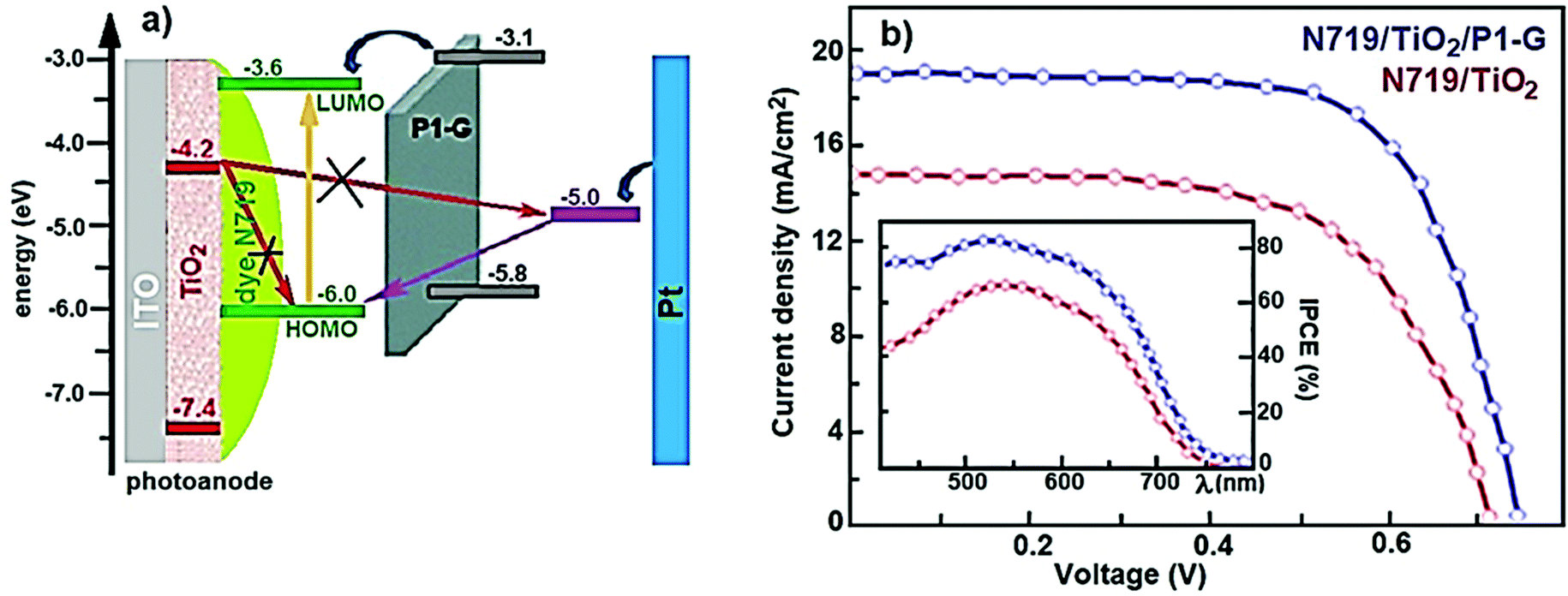 | ||
| Fig. 13 (a) Schematic of the energy-level diagram and electron transfer process in P1-graphene-based DSSCs. (b) J–V curves and IPCE spectra for DSSCs with and without a P1-G layer. Adapted with data from ref. 769. | ||
Fig. 14 summarizes the J–V curves of representative DSSCs using TiO2-GRMs composite-based photoanodes, compared to those of the equivalent TiO2-based cells, and the corresponding Dn and τ data.
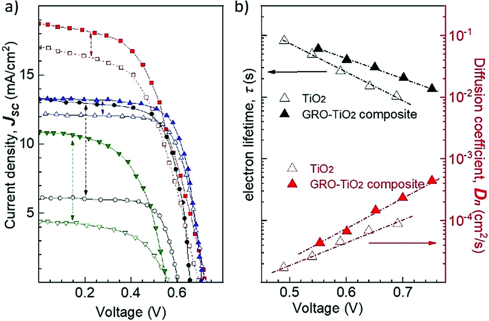 | ||
| Fig. 14 (a) Typical J–V curves of DSSCs based on different GRM-based photoactive layers (line and full symbols) compared to those of the corresponding traditional TiO2-based photoelectrode. (b) Electron diffusion coefficient (Dn) and lifetime (τ) dependence on the applied voltage for DSSCs based on TiO2 photoactive layers with and without GRMs. Adapted from ref. 741,742,758,759. | ||
Table 6 lists the experimental results achieved in DSSCs using solution-processed GRMs as the photoanode material. For each case, the η value is compared with that of the TiO2-based photoanode reference.
| Photoanode structure | Dye | Cell performance | Δη (%) | Ref. | |||
|---|---|---|---|---|---|---|---|
| J SC (mA cm−2) | V OC (V) | FF (−) | η (%) | ||||
| TiO2 | N3 | 11.26 | 0.69 | 64.5 | 5.01 | 39.1 | 703 |
| TiO2/GO (0.6 wt%) | 16.29 | 0.69 | 62.0 | 6.97 | |||
| TiO2 | N719 | 18.83 | 0.684 | 46.48 | 5.98 | 14.7 | 754 |
| TiO2/graphene (1 wt%) | 19.92 | 0.704 | 48.86 | 6.86 | |||
| TiO2 | N719 | 11.0 | 0.71 | 74.1 | 5.78 | 29.6 | 740 |
| TiO2/graphene (1.2 wt%) | 14.4 | 0.68 | 76.80 | 7.49 | |||
| TiO2 nanofibers | N719 | 13.9 | 0.71 | 63 | 6.3 | 20.6 | 772 |
| TiO2 nanofibers/graphene (0.7 wt%) | 16.2 | 0.71 | 66 | 7.6 | |||
| TiO2 | N719 | 8.69 | 0.77 | 66 | 4.42 | 36.9 | 773 |
| TiO2/graphene (1.0 wt %) | 12.89 | 0.68 | 69 | 6.05 | |||
| TiO2 | N3 | 8.787 | 0.606 | 65.97 | 4.43 | 14.9 | 756 |
| TiO2/GO | 10.284 | 0.616 | 63.75 | 5.09 | |||
| TiO2 | N3 | 9.58 | 0.82 | 62 | 4.89 | 32.7 | 707 |
| TiO2/graphene (0.5 wt%) | 12.78 | 0.82 | 62 | 6.49 | |||
| TiO2 | N719 | 10.99 | 0.68 | 71.3 | 5.3 | 34 | 774 |
| TiO2/graphene (0.2 wt%) | 13.93 | 0.70 | 73.4 | 7.1 | |||
| TiO2 | N719 | 13.2 | 0.691 | 52.4 | 4.78 | 60.1 | 775 |
| TiO2/RGO (1.6 wt%) | 18.39 | 0.682 | 61.2 | 7.68 | |||
| TiO2 | N719 | 10.75 | 0.686 | 56.6 | 4.2 | 31.0 | 776 |
| TiO2/RGO (0.75 wt%) | 12.16 | 0.668 | 67.7 | 5.5 | |||
| TiO2 | N719 | 6.18 | 0.606 | 71 | 2.67 | 110.5 | 741 |
| TiO2/RGO (0.25 wt%) | 13.04 | 0.645 | 67 | 5.62 | |||
| TiO2 | N719 | 12.5 | 0.669 | 66.0 | 5.52 | 17.6 | 777 |
| TiO2/graphene (0.5 wt%) | 13.7 | 0.685 | 69.2 | 6.49 | |||
| TiO2 | N719 | 16.13 | 0.62 | 65.3 | 6.57 | 778 | |
| N-Doped TiO2 | 16.71 | 0.74 | 61.6 | 7.64 | 16.3 | ||
| N-Doped TiO2/GO (0.1 wt%) | 19.65 | 0.74 | 64.70 | 9.32 | 41.9 | ||
| TiO2 | N719 | 10.30 | 0.64 | 73 | 4.81 | 29.3 | 779 |
| TiO2/GQDs | 11.72 | 0.68 | 78 | 6.22 | |||
| TiO2 | N719 | 12.59 | 0.704 | 65.07 | 5.77 | 780 | |
| TiO2/RGO (0.6 wt%) | 14.52 | 0.697 | 68.22 | 6.91 | 19.8 | ||
| TiO2/graphene sheets (0.6 wt%) | 17.31 | 0.690 | 69.04 | 8.24 | 42.8 | ||
| Pristine TiO2 | N719 | 11.1 | 0.693 | 67.7 | 5.21 | 45.1 | 781 |
| TiO2/graphene (0.03 wt%) | 16.5 | 0.703 | 65.2 | 7.56 | |||
| TiO2 | N719 | 10.7 | 0.75 | 76.82 | 6.13 | 11.7 | 782 |
| TiO2 RGO (3.12 wt%) | 12.9 | 0.76 | 69.20 | 6.85 | |||
| TiO2 nanotubes (TT) | N719 | 9.19 | 0.71 | 61.3 | 4.00 | 33.3 | 783 |
| TT/RGO (2 wt%) | 10.7 | 0.78 | 63.9 | 5.33 | |||
| TiO2 | N719 | 15.5 | 0.71 | 0.68 | 7.51 | 38.9 | 769 |
| TiO2/P1-graphene | 19.8 | 0.74 | 0.71 | 10.43 | |||
| TiO2 | N719 | 17.46 | 0.75 | 0.66 | 8.69 | 764 | |
| TiO2/GO | 16.70 | 0.74 | 0.68 | 8.55 | −1.6 | ||
| TiO2/NiO/NGE | 19.04 | 0.76 | 0.67 | 9.75 | 12.2 | ||
| TiO2 | N719 | 11.51 | 0.72 | 0.66 | 5.52 | 37.1 | 784 |
| TiO2/RGO | 16.75 | 0.74 | 0.65 | 7.57 | |||
| ZnO | N719 | 3.0 | 0.45 | — | 3.7 | 76.2 | 785 |
| ZnO/B-doped GQDs | 7.5 | 0.43 | — | 2.1 | |||
| TiO2 | N719 | 9.30 | 0.68 | 0.48 | 3.0 | 173.3 | 786 |
| TiO2/graphene | 27.49 | 0.67 | 0.45 | 8.2 | |||
| TiO2 nanofibers | N719 | 14.0 | 0.73 | 0.72 | 7.3 | 21.9 | 787 |
| TiO2 nanofibers/graphene | 18.0 | 0.73 | 0.68 | 8.9 | |||
| TiO2 | N719 | 13.3 | 0.82 | 0.58 | 6.32 | 36.4 | 788 |
| TiO2/RGO | 20.6 | 0.79 | 0.53 | 8.62 | |||
| TiO2 | Mimosa pudica | 0.059 | 69.5 | 789 | |||
| TiO2/RGO | 16.085 | 0.248 | — | 0.1 | |||
| SnO2:TiO2 | N719 | 7.76 | 0.67 | 0.56 | 2.91 | 15.8 | 790 |
| Graphene-doped SnO2:TiO2 | 9.03 | 0.65 | 0.58 | 3.37 | |||
| MoS2 | N719 | 9.32 | 0.67 | 0.52 | 3.36 | 165 | 791 |
| MoS2/graphene nanocomposite | 15.82 | 0.82 | 0.71 | 8.92 | |||
5.2 CEs
Functionalized graphene sheets (FGSs), containing lattice defects and oxygen functional groups (e.g., OH, CO, and epoxides), were thermally treated at a temperature of 1000–1500 °C to heal the lattice defects and tune the C/O ratio and used as the CEs.712 FGS-based inks were directly cast on a nonconductive plastic substrate without the need of a conductive substrate.712 The corresponding DSSCs based on FGS/surfactant/polymer network produced via the thermolysis process displayed an η value of 4.99%, which was close to that of Pt-based DSSCs (5.48%).712 Electrochemical impedance spectroscopy (EIS) and CV measurements suggested that RCT increases with decreasing O-containing functional groups, lowering the PV performance.712 Therefore, CE with C/O ratio of <7 was not sufficiently conductive for use as a CE material.712
In addition, it was proved that a low C/O ratio gives rise to a coarse film structure because of increased agglomeration.712 All these results proved that the optimization of functionalization/morphology is crucial to control the RCT, realizing low-cost and flexible CEs. By applying graphene-based CEs (namely, GNP-based CES) to the most advanced DSSC configurations, Kakiage et al. reached the current record η value for DSSCs, i.e., 14.7%.830 Noteworthily, the previous record η of 13.0% was also achieved using graphene-based CEs.831
Table 7 summarizes the PV parameters of selected DSSC configurations using solution-processed graphene-based CEs.
| Materials | Device structure | Cell performance | Ref. | ||||
|---|---|---|---|---|---|---|---|
| R CT (Ω cm2) | J SC (mA cm2) | V OC (V) | FF (−) | η (%) | |||
| Graphene | FTO/TiO2/N719/I−/I3−/graphene | 38.0 | 14.3 | 0.54 | 0.653 | 5.69 | 819 |
| TiN/graphene | FTO/TiO2/dye/I−/I3−/TiN-graphene | 5.67 | 12.34 | 0.73 | 0.643 | 5.78 | 802 |
| Pt/graphene | FTO/TiO2/N719/I−/I3−/Pt-graphene | 0.67 | 12.06 | 0.79 | 0.67 | 6.35 | 813 |
| GNPs | FTO/TiO2/Y123/Co2+/3+/GNPs | 0.70 | 12.70 | 1.03 | 0.70 | 9.30 | 796 |
| Pt-RGO | FTO/TiO2/dye/I−/I3−//Pt-RGO | — | 14.10 | 0.72 | 0.67 | 6.77 | 820 |
| GNSs/AC | FTO/TiO2/N719/I−/I3−/GNSs-AC | 0.5 ÷ 0.8 | 13.30 | 0.76 | 0.738 | 7.50 | 821 |
| NGNPs | FTO/TiO2/dye/Co(III/II)/NGNPs | 1.73 | 13.83 | 0.883 | 0.742 | 9.05 | 801 |
| GNTs/graphene-Rib | FTO/TiO2/N719/I−/I3−/GNT/graphene-Rib | — | 16.73 | 0.730 | 0.670 | 8.23 | 806 |
| GQD-PPy | FTO/TiO2/N719/I−/I3−/GQD-doped PPy | — | 14.36 | 0.723 | 0.580 | 5.27 | 822 |
| Au/GNP | FTO/TiO2/ADEKA-1/LEG4/Co2+/3+/Au/GNP | — | 19.55 | 0.995 | 0.776 | 14.7 | 829 |
| NGNPs | FTO/TiO2/YD2-o-C8/Co2+/3+/NGNPs | 0.45 | 13.33 | 0.870 | 0.720 | 8.30 | 823 |
| aGNP | FTO/TiO2/N719/I−/I3−/aGNP | 2.68 | 22.54 | 0.73 | 0.47 | 7.7 | 824 |
| Pt/GONF | FTO/TiO2/Y123/Cu +/Cu + +/Pt/GONF | 1.1 | 14.01 | 1.02 | 0.665 | 9.5 | 825 |
| PEDOT/RGO | FTO/TiO2/N719/I−/I3−/PEDOT-RGO | 18.17 | 15.82 | 0.73 | 0.67 | 7.79 | 826 |
| 3D graphene networks/RGO | FTO/TiO2:RGO/N719/I−/I3−/3D graphene networks/RGO | 9.61 | 21.0 | 0.75 | 0.661 | 9.79 | 827 |
| RGO QDs | FTO/TiO2/N719/I−/I3−/RGO QDs | 64.8 | 6.1 | 0.784 | 0.52 | 2.5 | 828 |
| GO | FTO/TiO2/N719/I−/I3−/GO | 52.26 | 11.83 | 0.66 | 0.715 | 5.6 | 829 |
| CVD graphene/FLG | FTO/TiO2/Y123/Co2+/3+/FLG/CVD graphene | — | 11.23 | 0.958 | 0.47 | 5.09 | 406 |
| GNPs | FTO/TiO2/SM315Co(bpy)3]2+/3+/GNPs | — | 18.1 | 0.91 | 0.78 | 13.0 | 830 |
Freitas et al. prepared MoS2 through a hydrothermal route to be used as the CE material using I−/I3− as the redox couple.835 MoS2-based DSSCs reached an η value of 2.9%, while DSSCs based on Pt CE has shown η = 5.2%.834 Although the η value of MoS2-based DSSCs was lower than that of Pt-based DSSCs, the possibility to dry MoS2-based CE at a temperature of 120 °C was considered to be an advantage for the manufacturing of low-cost Pt-free DSSCs.834 Next, Al-Mamun et al. grew ultrathin MoS2-nanostructured films onto the FTO substrate through a facile one-pot hydrothermal method.836 It was demonstrated that the temperature of the hydrothermal reaction and the molar ratio of reaction precursors have a relevant effect on the structure of the resulting MoS2.835 An ultrathin MoS2 film was obtained through a hydrothermal process with a reaction solution comprising NH2CSNH2 and (NH4)6Mo7O24·4H2O with a molar ratio of 28:1 at 150 °C for 24 h.835 After calcination at 400 °C in Ar, the resulting MoS2 films were used as CEs for DSSCs, reaching an η value of 7.41%.835 This value was superior to that measured for Pt-based DSSCs (7.13%).835 Meanwhile, homogeneous CNTs-MoS2-C with ultrathin, uniform lamellar structure of MoS2 was synthesized by Liu et al. via wet impregnation and calcination method.837 This work indicated that the addition of a nonionic surfactant (PEG400) promotes the dispersion of (NH4)2MoS4 onto the surface of CNTs, inhibiting the formation of independent particles of MoS2. The DSSCs using CNTs-MoS2-C composite-based CE achieved an η value of 7.23%, which was higher than that of Pt-based DSSCs (6.19%). Yue et al. synthetized flower-like structure complexes of MoS2/SWCNTs with glucose and PEDOT:PSS-assisted in situ hydrothermal route.838
Dye-sensitized solar cells based on MoS2/SWCNTs as the CE exhibited an η value of 8.14%, superior to that of Pt-based DSSCs (7.78%).837 Kim et al. used atomically thin 2D MoS2 nanoflakes, produced by a simple intercalation/exfoliation process, for fabricating transparent CEs via spin coating of the MoS2 dispersion followed by thermal treatment.839 The authors found that DSSCs based on MoS2 thermally treated at 100 °C exhibited an η value of 7.35%, which was comparable to that of the reference one, i.e., Pt-based DSSC (η = 7.53%).838,840 Solution-processed mesoporous WO3 films with 3D, rough, and high-curvature surfaces followed by a rapid sulfurization process to prepare an edge-oriented WS2 thin film was presented (Fig. 15). The maximized active edge sites on the high-curvature surface and electron transfer via continuous WS2 building blocks enhanced the catalytic activity toward the I3− reduction reaction in WS2-based CEs.839 This feature allowed WS2-based DSSCs to reach an η value of 8.85%, i.e., superior to that of the Pt-based reference (7.20%).839 More recently, Vikraman et al. proposed a synthesis route to fabricate MoS2/FTO CE via a simple chemical bath (pH ≈ 10) deposition process by means of thiourea (CH4N2S, 0.5 M) as the sulfur source and ammonium-heptamolybdate-tetrahydrate ((NH4)6Mo7O24·4H2O, 0.01–0.03 M), followed by annealing (450 °C for 60′) in a S environment to obtain crystalline MoS2.841 Under these conditions, the following reactions have been suggested: (1) CH4N2S + 2H2O → CO2↑ + 2NH3↑ + H2S↑; (2) (NH4)6Mo7O24·4H2O + 28H2S + 8NH3 → 7(NH4)2MoS4 + 28H2O; (3) (NH4)2MoS4 + 2N2H4 → MoS2 + N2↑ + 2(NH4)2S.840
 | ||
| Fig. 15 Schematic of the preparation of solution-processed mesoporous WO3 thin film and its conversion to edge-oriented WS2 thin film. Adapted from ref. 839. | ||
Raman spectroscopy, XPS, and scanning electron microscopy (SEM) analyses evidenced the presence of tri- and tetra-layered MoS2 and agglomeration effects, depending on the molybdate concentration and deposition time, respectively.840 Mo precursor concentration of 0.01 M and bath temperature and deposition time of 90 °C and 5′, respectively, led to the optimal morphology of MoS2 layers with spherical-shaped grains and absence of agglomeration effects.840 In addition, agglomerations of uniform spherical grains provide large SSA with numerous edge sites, thereby promoting the electrocatalytic activity.840 In this context, a deposition time of 30 min resulted in the optimal performance of DSSCs using the MoS2/FTO CE.840 Under longer deposition times (∼45 min), MoS2 changed from the layered to bulk structure, showing a phase transformation from MoS2 to Mo2S3.840 These effects lowered the catalytic activity of the CE due to the presence of an insufficient number of sulfur active sites in the material structure.840 In addition, MoS2/FTO CE has shown an electrocatalytic activity toward I3− reduction, corresponding to RCT (∼8.3 Ω □−1) comparable to that of Pt/FTO (∼7.2 Ω □−1).840 The PV performance of optimized MoS2/FTO-based DSSCs (JSC = 15.92 mA cm−2, VOC = 0.73 V, FF = 0.61, and η = 7.14%) almost reached that of the reference one based on Pt/FTO CE (JSC = 17.84 mA cm−2, VOC = 0.71 V, FF = 0.69, and η = 8.73%).840Fig. 16 compares the J–V curves of the MoS2/FTO and Pt/FTO CE-based DSSCs under the same illumination conditions.840 The anodic and cathodic branches of the Tafel polarization curves (Fig. 16, inset) indicate that the catalytic activity of MoS2/FTO and Pt/FTO CEs is comparable.840 In fact, larger the slope in the anodic/cathodic branch, higher are the exchange current densities on the electrode, which then shows higher electrocatalytic activity and lower RCT at the electrolyte/CE interface (see eqn (3.5)).842
 | ||
| Fig. 16 J–V curves of DSSCs with MoS2/FTO and Pt/FTO CEs. Inset shows the Tafel polarization curves of symmetrical cells with MoS2/FTO and Pt/FTO CEs. Adapted from ref. 840. | ||
Recently, MoSe2/WS2 heterostructures on FTO have been proposed as the DSSC anode, providing a simple route to optimize interfacial transport for enhancing the electrocatalytic properties of DSSC anodes. By optimizing the thickness of the WS2 layer, a maximum η value of 9.92% was reached, proving the potential of combining TMDs in advanced functional structured anodes.843
Table 8 summarizes the PV performance obtained in DSSCs using solution-processed TMD-based CEs.
| Material | Device structure | Cell performance | Ref. | ||||
|---|---|---|---|---|---|---|---|
| R CT (Ω cm2) | J SC (mA cm−2) | V OC (V) | FF (−) | η (%) | |||
| MoS2 catalyst | FTO/TiO2/N719/I−/I3−/MoS2/FTO | 0.50 | 13.84 | 0.76 | 0.73 | 7.59 | 833 |
| WS2 catalyst | FTO/TiO2/N719/I−/I3−/WS2/FTO | 0.30 | 14.13 | 0.78 | 0.70 | 7.73 | 833 |
| Carbon-coated WS2 | FTO/TiO2/N719/I−/I3−/WS2/FTO | 5.0 | 13.10 | 0.67 | 0.62 | 5.5 | 846 |
| NbSe2 nanorods | FTO/TiO2/N719/I−/I3−/NbSe2/FTO | 6.21 | 13.94 | 0.76 | 0.64 | 6.78 | 846 |
| NbSe2 nanosheets | FTO/TiO2/N719/I−/I3−/NbSe2/FTO | 2.59 | 15.04 | 0.77 | 0.63 | 7.34 | 847 |
| NbSe2 nanosheets | FTO/TiO2/N719/I−/I3−/NbSe2/FTO | — | 16.85 | 0.74 | 0.62 | 7.73 | 848 |
| NbSe2 nanorods | FTO/TiO2/N719/I−/I3−/NbSe/FTO | — | 14.85 | 0.74 | 0.46 | 5.05 | 847 |
| NbSe2 nanoparticles | FTO/TiO2/N719/I−/I3−/NbSe2/FTO | — | 14.93 | 0.75 | 0.55 | 6.27 | 847 |
| Porous MoS2 sheets | FTO/TiO2/N719/I−/I3−/MoS2/FTO | 1.73 | 15.40 | 0.763 | 0.53 | 6.35 | 849 |
| MoS2 nanoparticles | FTO/TiO2/N719/I−/I3−/MoS2/FTO | 93.0 | 14.72 | 0.745 | 0.490 | 5.41 | 850 |
| MoS2 | FTO/TiO2/N719/I−/I3−/MoS2/FTO | 18.50 | 18.46 | 0.680 | 0.580 | 7.01 | 851 |
| MoS2 nanosheets | FTO/TiO2/N719/I−/I3−/MoS2/FTO | 0.619 | 18.37 | 0.698 | 0.578 | 7.41 | 835 |
| MoSe2 | FTO/TiO2/N719/I−/I3−/MoSe2/FTO | 229.8 | 13.0 | 0.67 | 0.68 | 5.90 | 852 |
| NiS2 | FTO/TiO2/N719/I−/I3−/NiS2 | 50.40 | 14.70 | 0.72 | 0.52 | 5.50 | 851 |
| NiSe2 | FTO/TiO2/N719/I−/I3−/NiSe2 | 45.00 | 14.30 | 0.75 | 0.68 | 7.30 | 851 |
| CoSe2 | FTO/TiO2/N719/I−/I3−/CoSe2 | 10.70 | 13.50 | 0.72 | 0.68 | 6.60 | 851 |
| MoSe2 | FTO/TiO2/N719/I−/I3−/MoSe2 | 2.43 | 14.11 | 0.73 | 0.65 | 6.70 | 853 |
| WSe2 | FTO/TiO2/N719/I−/I3−/WSe2 | 0.78 | 15.50 | 0.73 | 0.66 | 7.48 | 852 |
| TaSe2 | FTO/TiO2/N719/I−/I3−/TaSe2 | 1.89 | 15.81 | 0.73 | 0.64 | 7.32 | 852 |
| MoS2 | FTO/TiO2/N719/I−/I3−/MoS2/FTO | 30.98 | 16.90 | 0.727 | 0.517 | 6.35 | 854 |
| MoS2 | FTO/TiO2/N719/I−/I3−/1 T-MoS2/FTO | 19.0 | 8.76 | 0.730 | 0.520 | 7.08 | 855 |
| MoS2 | FTO/TiO2/N719/I−/I3−/MoS2/FTO | 15.29 | 14.94 | 0.718 | 0.67 | 7.19 | 856 |
| MoS2 | FTO/TiO2/N719/I−/I3−/MoS2/FTO | 12.9 | 16.96 | 0.74 | 0.66 | 8.28 | 857 |
| MoS2 | FTO/TiO2/N719/I−/I3−/1T-MoS2/FTO | 19.60 | 11.54 | 0.80 | 0.65 | 6.0 | 858 |
| TiS2 | FTO/TiO2/N719/I−/I3−/TiS2/FTO | 0.63 | 17.48 | 0.73 | 0.603 | 7.66 | 859 |
| MoS2 | FTO/TiO2/N719/I−/I3−/MoS2/graphite paper | 2.16 | 13.34 | 0.696 | 0.698 | 6.48 | 860 |
| MoS2 | FTO/TiO2/N719/I−/I3−/MoS2/FTO | 2.77 | 15.68 | 0.72 | 0.634 | 7.16 | 861 |
| MoS2 | FTO/TiO2/N719/I−/I3−/MoS2/FTO | 25.77 | 15.92 | 0.73 | 0.615 | 7.14 | 862 |
| MoS2 | FTO/TiO2/N719/I−/I3−/MoS2/FTO | 2.86 | 19.6 | 0.795 | 0.36 | 6.6 | 863 |
| MoSe2/WS2 | FTO/TiO2/N719/I−/I3−/MoSe2/WS2/FTO | 18.3 | 23.1 | 0.69 | 0.651 | 9.92 | 842 |
Liu et al. also reported MoS2/graphene hybrid as the CE material.864 The hybrids were synthesized by mixing GO nanosheets with ammonium tetrathiomolybdate and converting the solid intermediate into MoS2/RGO hybrid by flowing H2 at 650 °C.863 The DSSCs using MoS2/RGO hybrid CE have shown excellent electrocatalytic activity toward I3− reduction, together with optimal electrochemical stability.863 CV and EIS measurements evidenced the superior electrocatalytic activity and lower RCT (0.57 Ω cm2) of the MoS2/RGO-based CE compared to the CEs based on RGO, MoS2, and sputtered Pt.863 The DSSCs assembled with MoS2/RGO CEs have shown PV characteristics (η = 6.0%, JSC = 12.51 mA cm−2, VOC = 0.73 V, and FF = 0.66) comparable to those of Pt-based DSSCs (JSC = 13.42 mA cm−2, VOC = 0.72 V, FF = 0.66, and η = 6.38%).863 Li et al. prepared RGO-NiS2 NP hybrids to develop CEs with excellent electrocatalytic activity toward I3− reduction.865 The fabricated DSSCs using the NiS2/RGO-based CE exhibited an η value of ∼8.55%, which was higher than that of the DSSC using either NiS2-based (∼7%) or RGO-based (∼3.14) CE, as well as Pt-based CE (∼8.15%).864
The DSSCs using CE based on NiO NPs/RGO hybrids have shown an η value of ∼7.42%, which was comparable to that of a conventional Pt-based DSSC (∼8.18%).866
The NiO NPs/RGO hybrids exhibited lower Rct value (1.93 Ω cm2) compared to those based on NiO-based (44.39 Ω cm2) and GO-based (12.19 Ω cm2) CEs.865 Experimental investigations indicated that the synergic effects of two different low-dimensional carbon materials, such as CNT/graphene nanoribbons (CNT/graph-nRib), can be used to further amplify the CE catalytic activity of the single nanomaterial.806
More recently, Zhai et al. obtained an η value of ∼8.3% in porphyrin-sensitized DSSCs using N-doped GNP-based CE [Co-(bpy)3]3+/2+ redox complexes.822 The obtained result was the consequence of better electrocatalytic activity in comparison to that of the Pt-based CE, whose corresponding cell reached an η value of 7.95%.822 The performance increase was ascribed to a higher number of catalytic sites, due to the introduction of pyridinic and pyrrolic N into the carbon-conjugated lattice, compared to the GNPs.822
Shen et al. synthesized NiS/RGO-based CE with a material mass ratio varying from 0.2 up to 0.6 through a low-temperature hydrothermal method.867 The NiS/RGO hybrid-based CE exhibited the best catalytic property for the NiS:RGO mass ratio of 0.4%, yielding a DSSC with an η value of 8.26%, a value much higher than that of pristine RGO-based or NiS-based references (1.56% and 7.41%, respectively).866 The obtained results demonstrated that a correct load of NiS hinders the agglomeration of RGO flakes, favoring the diffusion of electrolyte into the NiS/RGO network.866
Zhou et al. synthesized graphene-wrapped CuInS2 hybrids to be used as the CE material.868 The DSSCs based on CuInS2/RGO as CE achieved an η value of 6.4%, which was comparable to that of Pt-based CE (6.9%).867 Huo et al. developed a sponge-like CoS/RGO-based CE with a low RCT value of 3.59 Ω cm2.869 The corresponding DSSCs have shown an η value of 9.39%.868
Li et al. synthesized a nanostructured architecture of 3D bismuth sulfide (Bi2S3) microspheres on RGO through a solvothermal route.877 The as-produced architecture was used as the CE for DSSCs.876 By combining the characteristics of direct-bandgap Bi2S3 semiconductor (low bandgap of 1.7 eV and absorption coefficient of the order of 104–105 cm−1) with outstanding carrier transfer properties of RGO, an η value ∼3 times greater than that of DSSCs with 3D Bi2S3 without RGO (1.9%) was achieved.
Chen et al. prepared GQDs through a chemical oxidation approach to dope conductive polymers (polypyrrole (PPy)) on FTO glass as the CE for DSSCs.821 The as-prepared DSSCs displayed an η value (i.e., 5.27%) lower than that of Pt-based reference devices (η ≈ 6.02%), but ∼20% higher compared to that of DSSCs based on PPY as the CE (4.46%).821
Murugadoss et al. grew NiSe NPs on GNSs with different mass ratios to obtain NiSe/GNSx (x = 0.25 to 1.00) nanohybrids by an in situ hydrothermal process.878 This method takes advantages of the high SSA of GNSs to homogeneously immobilize NiSe NPs on top of them acting as the catalytic sites.877 The nanohybrid with a mass ratio of 1:0.50 (NiSe/GNS0.50) exhibited the highest electrocatalytic activity and electrolyte diffusion among the different hybrid compositions.877 Thus, the DSSC with NiSe/GNS0.50 CE exhibited an η value of 8.62%, which is higher compared to a standard Pt-based DSSC (η = 7.68%).877 The NiSe/GNS0.50 CE exhibited a superior PV performance compared to both Pt and pristine NiSe CEs.877 Compared to the hybrid NiSe/GNS0.50 CE, the lower performance of the NiSe electrode, when integrated in a DSSC (η = 7.18%), was attributed to the aggregation of NiSe NPs and the poor connections between the NPs, which decrease the number of electrocatalytic active sites as well as the electrical conductivity of the CE.877 The optimal performance of NiSe/GNS0.50 CE is determined by the interfacial electron transfer pathways of GNSs and the exceptional catalytic activity of NiSe toward I3− reduction at the CE/electrolyte interface.877
Table 9 summarizes the PV performance of DSSCs using 2D material-based hybrid CEs.
| Material | Device structure | PV parameters | Ref. | ||||
|---|---|---|---|---|---|---|---|
| R CT (Ω cm2) | J SC (mA cm−2) | V OC (V) | FF (−) | η (%) | |||
| MoS2/graphene | FTO/TiO2/N719/I−/I3−/MoS2/graphene | 24.42 | 12.41 | 0.71 | 0.68 | 5.98 | 844 |
| GNS | FTO/TiO2/dye/I−/I3−/GNS | 6.24 | 11.99 | 0.754 | 0.30 | 2.68 | 843 |
| MoS2/GNS | FTO/TiO2/dye/I−/I3−/MoS2/GNS | 2.34 | 12.79 | 0.773 | 0.59 | 5.81 | |
| RGO/NiS2 | FTO/TiO2/N719/I−/I3−/NiS2/RGO | 2.90 | 16.55 | 0.749 | 0.69 | 8.55 | 864 |
| Bi2S3/RGO | FTO/TiO2/N719/I−/I3−/Bi2S3/RGO | 9.2 | 12.20 | 0.75 | 0.60 | 5.5 | 876 |
| RGO/NiO | FTO/TiO2/N719/I−/I3−/NiO/RGO | 1.93 | 15.57 | 0.763 | 0.624 | 7.42 | 865 |
| CuInS2/graphene | FTO/TiO2/N719/I−/I3−/CuInS2/graphene | 2.30 | 14.20 | 0.743 | 60.7 | 6.40 | 867 |
| CoS/RGO | FTO/TiO2/N719/I−/I3−/CoS/RGO | 3.59 | 19.42 | 0.764 | 0.633 | 9.39 | 868 |
| NiS/RGO | FTO/TiO2/N719/I−/I3−/NiS/RGO | 7.06 | 17.05 | 0.778 | 0.623 | 8.26 | 866 |
| MoS2/graphite | FTO/TiO2/dye/I−/I3−//MoS2/graphite | 8.05 | 15.64 | 0.685 | 0.67 | 7.18 | 870 |
| TiS2/graphene | FTO/TiO2/N719/I−/I3−/TiS2-graphene | 0.63 | 17.76 | 0.72 | 0.685 | 8.80 | 858 |
| WOx/carbon | FTO/TiO2/N719dye/I−/I3−/WOx/carbon/FTO | 12.70 | 14.30 | 0.705 | 0.591 | 6.00 | 871 |
| WOx@WS2/carbon | FTO/TiO2/N719dye/I−/I3−/WOx@WS2/carbon/FTO | 0.88 | 15.48 | 0.720 | 0.695 | 7.71 | 870 |
| MoS2/graphene | FTO/TiO2/N719dye/I−/I3−/MoS2/graphene/FTO | 34.02 | 20.5 | 0.800 | 0.42 | 8.1 | 862 |
| MoS2/SnS2 | FTO/TiO2/N719/I−/I3−/MoS2/SnS2/FTO | 0.32 | 15.99 | 0.73 | 0.65 | 7.6 | 872 |
| NiSe/GNS0.50 | FTO/TiO2/N719/I−/I3−/NiSe2-graphene (1:0.50) |
1.92 | 16.73 | 0.75 | 0.68 | 8.62 | 877 |
| WSe2/MoS2 | FTO/TiO2/N719/I−/I3−/WSe2/MoS2/FTO | 44.42 | 16.89 | 0.69 | 0.724 | 8.44 | 873 |
| Polyaniline/graphene | FTO/TiO2/N719/I−/I3−/polyaniline/graphene | 20.1 | 15.5 | 0.787 | 0.62 | 7.45 | 874 |
| NiO/NiS/graphene | FTO/TiO2/N719/I−/I3−/NiO/NiS/graphene | 23.2 | 4.86 | 0.76 | 0.56 | 2.10 | 875 |
| Co–Mo–S anchored on nitrogen-doped graphene (NG) | FTO/TiO2/N719/I−/I3−/Co–Mo–S anchored on nitrogen-doped graphene (NG) | — | 7.22 | 0.49 | 0.44 | 1.18 | 876 |
5.3 Summary and outlook
The global DSSC market size was valued at USD 90.5 million in 2019 and is expected to grow at a compound annual growth rate (CAGR) of 12.4% from 2020 to 2027.887 The global DSSC market is segregated into portable charging, BIPV, embedded electronics, outdoor advertising, and automotive. In this scenario, BIPV represents a strategic sector, in which DSSCs reached an η value higher than 25% (up to a record-high value of 32% at 1000 lux).888–890 Regarding outdoor applications, the advent of PSCs has outclassed the use of DSSCs as single-junction devices, the η value of DSSC being significantly inferior to that of PSCs.897 However, DSSCs still represent an interesting PV technology to make cost-effective and efficient tandem systems, including those based on PSCs as sub-cells. Overall, the advancements achieved in DSSCs using 2D materials might be applied to the most promising configuration for convenient applications, as discussed above. In fact, the current record-high η value of DSSCs was reached using GNPs as the CE829 (previous record of 13% was also achieved using graphene-based CEs),830 unequi VOC ally proving the potential of 2D materials for both improving the PV performance and decreasing the cost of traditional PV based on Pt CEs.891,892 Prospectively, lifecycle assessment can provide a useful methodological framework to calculate the eco-profiles of solution-processed 2D material-based DSSCs with a future-oriented perspective. Importantly, DSSCs are the third-generation hybrid–organic technology that reached the highest maturity in terms of manufacturing, reporting several pilot-line semi-industrial production lines.893,894 Overall, the synergistic use of 2D materials, novel dyes, and advanced anode structures are expected to play a major role in the further optimization of DSSC technology, both in the indoor and outdoor PV market.6. PSCs
During the last few years, the rapid emergence of perovskite PV technology in the global energy scenario has strongly attracted efforts from the scientific community.895–897Perovskite semiconductors have been used in SCs since the pioneering work of Kojima et al. who proposed the perovskite as a sensitizer in a DSSC, achieving an η value of 3.8%.894 Thereafter, much progress has been achieved in the last 12 years, achieving certified η exceeding 25%,898 which makes PSCs among the most promising class of devices in the broad context of 3rd-generation PV technologies.897
The term perovskite refers to a broad class of crystals sharing the crystalline structure of calcium titanate (CaTiO3).900 Generally, the crystallographic structure is indicated with the chemical formula ABX3, where A is a small organic or inorganic cation that occupies a cube-octahedral901 site, B is a metal cation in the center, and X is a halogen anion in an octahedral site.899
The perovskite structure widely used in SCs is an organic–inorganic hybrid based on an organometallic halide material. In particular, A can be methylammonium CH3NH3+ (MA), formamidinium (FA), or Cs; B is commonly the lead ion Pb2+ (even though ions of Sn, Ge, Sb, Bi are also used), and X is an halide, typically iodide or bromide (I− or Br−).902 Thus, in the perovskite structure, A, located in a cage, is surrounded by four BX6 octahedra, and can partially move inside the cage901 (Fig. 17). Organic–inorganic halide perovskites offer attractive prospects in developing high-performance SCs,903–905 low processing costs and facile fabrication processes.906,907 In fact, due to their particular crystallographic structure and the peculiar choice of components,908 organic–inorganic halide perovskites exhibit outstanding and unique optoelectronic properties, including large and broad absorption spectrum,909 immediate charge generation within the bulk material (due to very low exciton binding energy),910 optimal ambipolar charge transport with a long charge diffusion length (∼100 nm for CH3NH3PbI3 and ∼1 μm for CH3NH3PbI3−xClx),911 efficient charge injection into the CTLs, and low trap density, which points them as “defect-tolerant” materials.906,912–914 In addition, chemical modifications of the constituents enable the tuning of the material properties, for example, the Eg, which spans over a range wider than 1 eV. The architecture of a PSC consists of a perovskite active layer sandwiched between an HTL and an ETL. More specifically, two PSC structures have been mainly developed, i.e., mesoscopic894,906 and planar905 structures, and both of them can be found in n–i–p (direct) or p–i–n (inverted) configurations (Fig. 18).915 The mesoscopic architecture is so called because a mesoporous oxide layer is used as the ETL in which the perovskite is infiltrated.
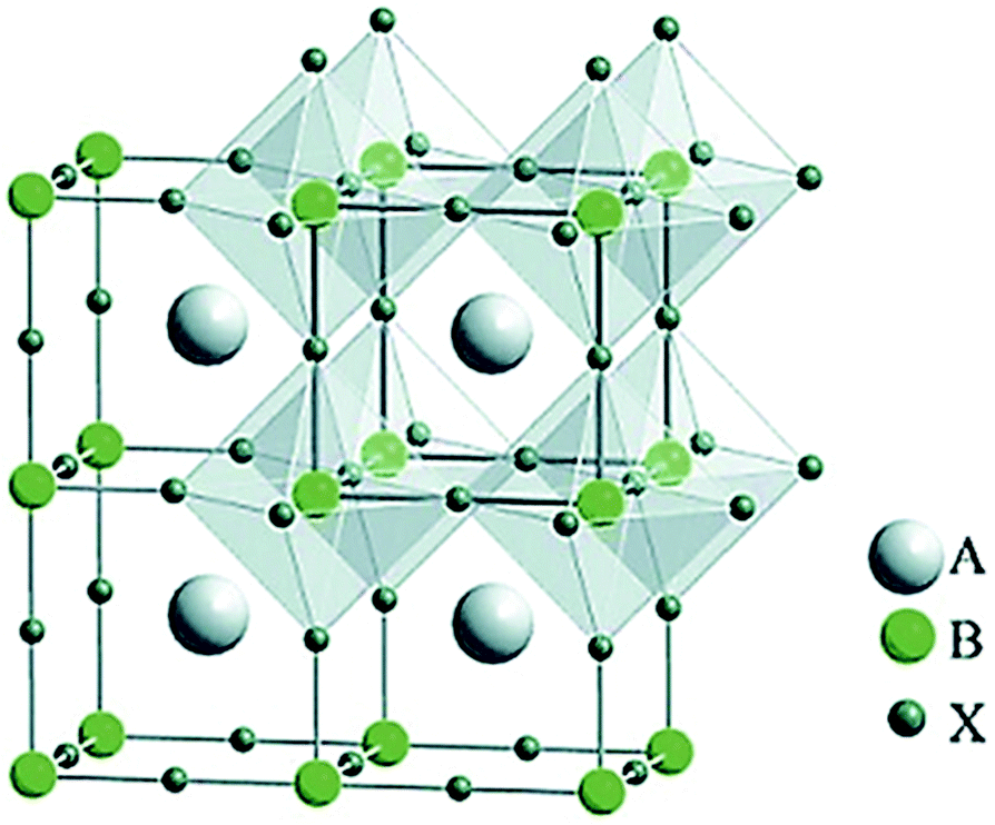 | ||
| Fig. 17 The basic perovskite structure (ABX3). Adapted from ref. 899. | ||
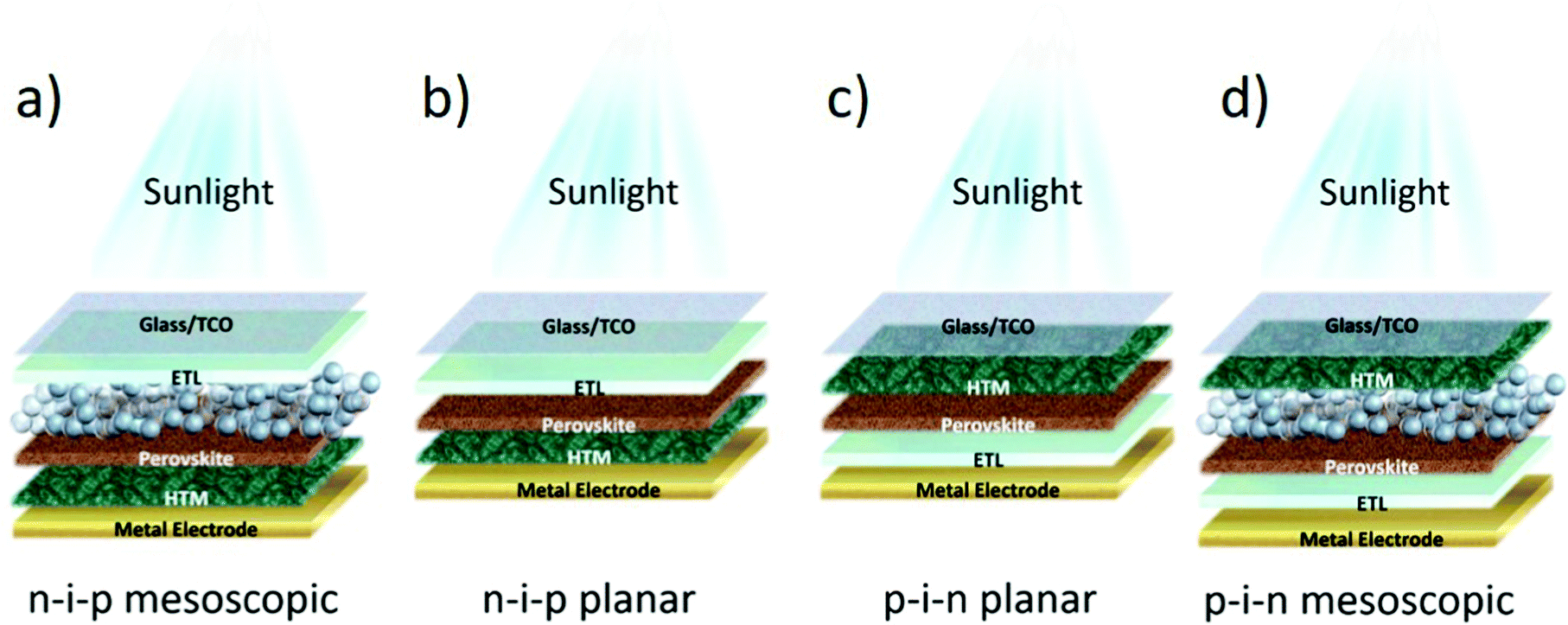 | ||
| Fig. 18 (a) Mesoscopic n–i–p, (b) planar n–i–p, and (c) planar p–i–n and mesoscopic p–i–n PSC structures. | ||
In detail, mesoscopic PSCs are composed of different layers.894,906,916 The first one is a TCE (e.g., FTO or ITO), deposited on the bottom of the glass surface and acting as the front transparent electrode. Subsequently, a compact ETL is deposited onto the TCE. The compact ETL is typically made of TiOx906 or ZnO917,918 (thickness ranging from 10 to 400 nm, depending on the material), which can be deposited using different techniques (e.g., spray pyrolysis,919 sol–gel,920 DC magnetron sputtering,921,922 electrodeposition,923,924 electron-beam evaporation,925 and pulsed laser deposition926,927). Then, a layer of mesoporous oxide is obtained by depositing a paste typically containing colloidal NPs (preferably TiO2,894,906 ZrO2,928,929 Al2O3,930 and SiO2931,932) using various techniques (e.g., sol–gel,933,934 doctor blade,935 spin coating,936 spray coating,937 electrospray deposition,938 slot-die coating,939,940 inkjet printing,941 and pulsed laser deposition733,942,943). For glassy substrates, the device is subsequently heated (e.g., at 450–550 °C for 30 min for the calcination of TiO2) in order to evaporate the organic binder and to create an electromechanical connection between the NPs.902,944 For heat-sensitive plastic substrates, the mesoporous layer is alternatively formed by means of low-temperature processes, such as microwave sintering,945 laser sintering,946,947 intense pulsed light sintering,948 and NIR sintering.949,950 Thereafter, a perovskite layer (generally formed by one or more organic cations, such as methylammonium (MA) and formamidinium (FA), and one or more inorganic compounds, such as PbI2Cl, Pb3, or PbI2Br) is infiltrated in the mesoporous electrodes by various techniques,951e.g., spin coating,902,952–955 spray casting,956–959 physical vapor deposition,960,961 thermal evaporation,962 dip coating,963 slot-die coating,964 roller coating,965 and bar coating.966 Subsequently, the resulting film is often crystallized through a heating step at 70–100 °C for 10–30 min, depending on the perovskite composition and deposition method.950 On the so-formed photoelectrode, an HTL (e.g., P3HT,967–969 spiro-OMeTAD,970,971 PTAA,972 PEDOT,973 copper thiocyanate (CuSCN),974,975 and triphenylamine-based molecules976,977) is deposited, typically via solution-based techniques, e.g., spin coating, spray casting, inkjet printing, and slot-die coating. Lastly, the mesoscopic PSC is completed by depositing a metal contact as the CE (e.g., Au, Ag, and Al). Alternatively, a planar architecture can be used as a simpler PSC structure.905 The main difference between a planar direct configuration (n–i–p structure) and mesoscopic devices is the use of a single compact n-type metal oxide layer (e.g., TiO2,978 ZnO,979–981 and SnO2982–986) in the former rather than a combination of both compact and mesostructured scaffolds.987,988 Differently, in an inverted planar configuration (p–i–n structure),905 a p-type material (e.g., NiOx,989–991 PEDOT:PSS,992,993 CuSCN,994 CuI,995 Cu oxides,996,997 and V2OX998) is used as the bottom HTL, while PCBM is the typically used ETL.999–1001 As a matter of fact, several potential material/structure combinations can be designed to implement new PSC structures. In fact, on one hand, the correct choice of materials is crucial for determining both optical and electronic properties (e.g., bandgap and commensurate absorption spectra, μ, charge diffusion lengths, etc.). On the other hand, material arrangement in the different architectures plays a crucial role in the overall PSC performance.
Despite the undoubted interest in perovskites, mainly owing to their low cost and efficiency compared to the technologies currently in the market, PSCs currently suffer from low stability, a big challenge for their market uptake.1002 Perovskite instability has been correlated to both intrinsic1003–1006 and extrinsic factors,1005 mainly associated with moisture1007,1008 and oxygen exposure,1006,1007 as well as UV radiation,1009,1010 high-temperature exposure,1011 and electrical biases.1012,1013 In detail, under prolonged working conditions, PSCs often exhibit structural degradation of perovskites (as well as other component layers). For example, ion migration from the perovskite to metal and vice versa, as well as perovskite decomposition through the volatilization of perovskite species can cause the rapid failure of PSCs.1005,1014
Although some extrinsic degradation factors, such as oxygen, moisture, and UV exposure can be avoided by means of new strategies to encapsulate the assembled device,1015–1017 the intrinsic structural instability can be addressed by designing more stable perovskites1018–1021 or by adding crosslinking additives,1022–1025 ionic liquids additives,1026–1028 dopants,1029–1031 and interlayers1032–1035 that can stabilize the crystal structure. Recently, pressure-tight polymer (polyisobutylene)/glass stack encapsulation has been shown to inhibit intake moisture, while preventing the outgassing of decomposition products of the perovskite.1016 Consequently, the decomposition reaction for a prototypical Cs-containing triple-cation perovskite, namely, Cs0.05FA0.8MA0.15Pb(I0.85Br0.15)3, were suppressed, permitting the devices to pass the International Electrotechnical Commission (IEC) 61215:2016 Damp Heat and Humidity Freeze tests.1016
In this context, (1) the exploitation of solution-processed GRMs to engineer the device interface1036–1040 and (2) the introduction of 2D perovskites as active materials111,1016,1041–1043 have recently been revealed as two main routes for the realization of highly efficient and durable PSCs. In the first case, the possibility to chemically or thermally modify GRMs allows their oxygen vacancy/defect/functional group concentration to be controlled to attain the desired optoelectronic properties.1044 Recent advances in the production and processing of GRMs allowed their effective use in the PSC structures,596,1037 for example, as ETLs1045–1047 or HTLs1048,1049 as well as interlayers at the perovskite/CTL interface.1050,1051 In particular, GRM-induced improvement in charge transport and collection at the electrodes allows the η value to be significantly enhanced.1052,1053 Moreover, the use of GRMs in PSCs results in a remarkable increase in the device's stability under several stress conditions, by preventing interfacial perovskite degradation.1039,1054–1059 In the second case, 2D perovskites have demonstrated superior moisture stability compared to the 3D counterparts, offering new approaches to stabilize PSCs.111,1060 Owing to their versatile structure, 2D perovskites enable the ad hoc tuning of their optoelectronic properties through compositional engineering.111,1061 Finally, recent achievements have demonstrated the possibility to combine 3D and 2D perovskites to simultaneously boost the device efficiency and stability, opening the route toward advanced mixed-dimensional PSCs.111,1062
In the subsequent sections, the use of GRMs and 2D perovskite layers into CTLs and perovskite, as well as their utilization as buffer layers and front/back electrodes, will be discussed.
6.1 ETLs
As shown in Fig. 18, the configurations of a PSC require a perovskite light-absorbing layer interposed between a wide-bandgap ETL and HTL, which assist charge carrier transport to the negative and positive electrodes, respectively.1063,1064 Meanwhile, the CTLs must prevent charge transport toward the undesired electrode.1062,1063In mesoscopic PSCs, the generated electrons have to travel through the mesoporous ETL, which plays a crucial role in terms of efficiency and stability of the whole device.1065,1066 A large variety of materials have been used as ETLs to efficiently extract photoexcited electrons in the perovskite layer.1067 It is worth pointing out that the mesoporous ETL can be conductive (e.g., TiO2, ZnO, and NiO) or insulating (e.g., Al2O3, ZrO2, and SiO2). In the first case, the mesoporous layer acts as an ETL, while in the second one, it provides a scaffold functionality.
Due to the capacity to prevent leakage currents, and hence to prevent cell shunting, TiO2 is the most established ETL for PSCs.696,1068 Mesoscopic PSCs using anatase mesoporous TiO2 (mTiO2) with NPs in the 10–30 nm size range have shown η often exceeding 21%.902,1069 Nanomaterials based on ZnO could also be promising semiconducting metal oxides alternative to TiO2, owing to their wide bandgap (∼3.37 eV), large exciton binding energy (∼60 meV), high μe, unique photoelectric properties, optical transparency, electric conductivity, and piezoelectric properties.1070–1072 To overcome the disruptive effect of moisture on the perovskite structure and to prolong the lifetime of the devices, ZnO QDs have also been exploited as an alternative scaffold to other ZnO nanostructures, owing to their tunable bandgap and chemical inertness.1073 Lastly, ZnO offers the benefit to be easily processed at low temperatures, opening the possibility to develop efficient low-temperature fabricated mesoscopic PSCs.1074
In order to increase the VOC of PSCs, mesoporous Al2O3, ZrO2, and SiO2 have been investigated as a scaffold to alternative mTiO2.1075–1078 For example, a mesoporous Al2O3 (mAl2O3) layer was used to transport photoexcited electrons throughout the perovskite layer, allowing η > 12% to be reached.1079
Ternary oxides, such as SrTiO3,1080,1081 Zn2SnO4,1082 and BaSnO31083 have also been used to obtain better performing devices in terms of η. For example, SrTiO3 exhibits the same perovskite structure with μe and CB higher than those of TiO2.1084,1085 Thus, SrTiO3-based PSCs showing VOC higher than 1 V have been reported.1080
In order to boost the electrical performance of PSCs, it is necessary to precisely control the charge carriers’ pathway along the entire device,1086,1087 by avoiding losses due to photon thermalization or carrier-trapping processes and improving faster electron injection. In fact, charge carrier injection at the perovskite/ETL interface is strongly limited by interfacial charge recombination when the interfaces are not properly engineered, such as in presence of nonoptimized energy-level alignment.1088 Likewise, poor charge transport in the CTLs1089,1090 severely limits charge collection toward the electrodes, reducing ISC and FF1091–1093 and therefore the η value.
Several strategies have been reported in the literature to enhance the charge transport and extraction properties at the interface between the perovskite/ETL. These strategies include TiO2 doping1094,1095 and the use of different TiO2 nanostructures,1096–1098 as well as the modification of interfacial energy-level alignment through the incorporation of appropriate buffer layers.1036,1099
In this framework, numerous solutions have been proposed to facilitate electron extraction and to increase the conductivity by taking advantage of GRMs.1036,1100–1102
The use of graphene with nanostructured ZnO or TiO2 in PSCs results in a higher photocurrent density and consequently better device performance compared to the reference device without graphene.1099 Wang et al. developed low-temperature-processed nanocomposites of pristine graphene nanoflakes and anatase–TiO2 NPs to be used as the ETL in mesoscopic PSCs (Fig. 19a).1100 The observed decrease in the series resistance, as well as a decrease in charge recombination, determined an improvement in the device performance, achieving an η value of 15.6% (Fig. 19b).1100 The use of graphene nanoflakes, with an appropriate ϕW (i.e., 4.4 eV), reduced the energy barrier between the LUMO of TiO2 (4.2 eV) and Φw of FTO (4.5 eV), leading to better electron collection through the ETL (Fig. 19c).1100 In addition, the μ value of graphene flakes increased the electrical conductivity of the graphene–TiO2 ETL compared to bare TiO2 (Fig. 19d).1100 GRMs have also been used as the interlayer between perovskite and mTiO2. Zhu et al. reported that the insertion of an ultrathin layer of GQDs between the perovskite and mTiO2 impacts the PSC performance, increasing the η value from 8.81% up to 10.15%.1101 The insertion of a GQD interlayer causes strong quenching of perovskite photoluminescence at ∼760 nm due to a reduced electron extraction time (90–106 ps) in the presence of GQDs.1101 This means that the GQDs permit an efficient electron transfer from the photo-absorber to the acceptor, resulting in efficient electron extraction.1101
 | ||
| Fig. 19 (a) Cross-sectional SEM image of a PSC based on a graphene–TiO2 composite as the ETL. (b) J–V curves measured for PSCs with different ETLs under solar irradiation and in the dark (c). Energy levels of a PSC based on a graphene–TiO2 composite as the ETL. (d) Series resistances of PSCs using pristine TiO2 and graphene–TiO2 composite as the ETLs. Reprinted with permission from ref. 1100, Copyright 2013, American Chemical Society. | ||
More recently, Tavakoli and co-workers developed a new and simple chemical process to synthesize a quasi-core–shell structure of ZnO NPs/RGO to be used as the ETL in PSCs.1099 In fact, RGO passivates the ZnO NP surface, preventing degradation reactions at the perovskite/ETL interface caused by the presence of the hydroxide group.1099 Furthermore, the ZnO/RGO ETL improves the electron transfer at the perovskite/ETL interface, increasing the EQE and photocurrent density.1099 Thus, the use of RGO increased η up to 15.2% on rigid PSCs using FTO-coated substrates, while flexible devices on ITO-coated PET achieved an η value of 11.2%.1099 In a subsequent work, Tavakoli et al. reported a very high performing PSC (η = 17.2%) using a reduced-graphene scaffold (rGS) obtained through EpD.1103 The authors fabricated a porous 3D scaffold of graphene with a large SSA that enabled a higher loading of perovskite materials.1102 The addition of rGS improved the carrier transport of the PSC, yielding an η value enhancement of ∼27% compared to the conventional device.1102 Besides, sealed rGS-based devices retained 80% of their initial η for a time as long as a month under ambient conditions (∼65% humidity).1102 Ameen and co-workers used a graphene thin film as the barrier layer between O2 plasma-treated ITO-PET and the ETL based on ZnO QDs.1104 A subsequent atmospheric plasma jet (APjet) treatment of ZnO QD ETL improved the interfacial contacts, modifying the surface properties of the ITO-PET/Gr/ZnO QD structure.1103 The use of a graphene interlayer and APjet treatment of ZnO QDs improved the carrier transport and collection efficiency.1103 Moreover, modification with regard to the surface area, pore size, and porosity caused by the APjet treatment allowed perovskite infiltration to be optimized.1103 Thus, the fabricated ITO-PET/Gr/ZnO QDs/CH3NH3PbI3/spiro-OMeTAD/Ag flexible PSCs reached a high η value of ∼9.73%, along with a JSC value of ∼16.8 mA cm−2, VOC of ∼0.935 V, and FF of ∼0.62.1103 These performances outperformed those of the PSCs fabricated with ITO-PET/graphene and ZnO-QDs/graphene/ITO-PET structures.1103 Graphene-based interface engineering through the incorporation of an additional buffer layer represents an effective strategy to improve the PV performance while overcoming oxygen- and moisture-induced instability. For example, Agresti et al. proposed a new, efficient PSC structure by including a GO-Li interlayer between TiO2 and the perovskite.1051 The main effect of the GO-Li interlayer is the enhancement—compared to the reference devices—of both JSC (+10.5%) and FF (+7.5%), positively affecting both η and long-term stability.1051 In particular, this work pointed out to improved charge extraction/injection at the negative photoelectrode when GO-Li was used as the ETL.1051 In fact, the GO-Li interlayer favors the passivation of oxygen defects/vacancies in mTiO2, eliminating reactive centers susceptible to moisture attack. Such an effect improved the stability of devices, which have shown an enlarged lifetime without encapsulation during aging tests. A similar interface strategy was used to further increase the η and stability of PSCs using mTiO2 doped with graphene flakes (mTiO2 + G) and GO as an interlayer between the perovskite and HTL.1036,1105 These PSCs achieved a remarkable η value of 18.2% as a consequence of the improved charge-carrier injection/collection.1036 In addition, the optimized PSCs improved their stability under several aging tests compared to the reference devices. In fact, when mTiO2 + G was used, the PSCs retained more than 88% of their initial η under prolonged 1 sun illumination at MPPT for a time as long as 16 h (Fig. 20a). Recently, time-of-flight secondary ion mass spectrometry (ToF-SIMS) 3D imaging and XPS depth profile analysis were used to evaluate the light-induced degradation of layers and interfaces both in mesoscopic PSCs with mTiO2 + G and graphene-free PSCs (Fig. 20b).1106 These results demonstrated that the incorporation of graphene within mTiO2 improves the stability of PSCs by limiting the light-induced back-conversion of CH3NH3PbI3 into PbIx and PbOx species.1105 Therefore, the formation of iodine species was also reduced, impeding them to diffuse across the interface until modifying the Au electrode and mTiO2 through the A–I and Ti–I bond formation.1105 Even more recently, femtosecond transient absorption measurements proved that the incorporation of graphene can stabilize the PSCs owing to the potential exploitation of the contribution of hot carriers to the η value of PSC (Fig. 20c).1107 In particular, these results demonstrated that the insertion of graphene flakes into mTiO2 leads to stable values of carrier temperature.1106 In graphene-free PSCs aged over 1 week, the carrier temperature decreased from 1800 to 1300 K, while the graphene-based cell reported a reduction inferior to 200 K after the same aging time.1106 The stability of carrier temperature was associated to the stability of the perovskite embedded in mTiO2 + G. Overall, all these results involving mTiO2 + G have opened the way for scalable large-area PSC production due to the use of GRMs in the form of dispersions and inks.205 In fact, by means of graphene and GRMs, Agresti et al. realized large-area (50.6 cm2) perovskite-based solar modules (PSMs) with a remarkable η value of 12.6%.1108
 | ||
| Fig. 20 (a) Graphene-based PSC energy-level alignment representation and η stability trends under prolonged light-soaking condition (1 sun) for both standard and graphene-engineered devices.1036 (b) ToF-SIMS 3D analysis showing the reconstructed XZ distribution of PbI3− (from the CH3NH3PbI3 absorber) in the as-deposited (upper part) and 24 h light-aged (lower part) PSCs. The PbI3 signal decay suggests the progressive decomposition of the perovskite absorber material, which was always more severe in the reference PSC structure. Adapted from ref. 1105, Copyright 2018, Elsevier. (c) Transient absorption spectra acquired at a pump–probe time delay of 0.75 ps for (a) as-prepared and (b) aged PSC with mTiO2 + G (PSC-G) and graphene-free PSC (PSC-NoG). The photobleaching signal exhibits two peaks at 1.64 eV and 1.66 eV attributed to the absorption bleaching in large crystals of the capping layer and in small crystals of the mesoporous layer, respectively. Hot electron lifetime from the transient absorption measurements related to the degradation of small perovskite crystals wrapped in the mesoporous TiO2 layer. When graphene is embedded into the mTiO2 layer, the hot-carrier temperature is preserved over aging time by improving the device stability. Adapted from ref. 1106, Copyright 2019, American Chemical Society. | ||
Recently, a similar approach was followed by Cho et al., which systematically investigated the role of RGO in PSCs by dispersing RGO into the mTiO2 matrix to obtain highly efficient PSC (η = 19.54%).1109 Moreover, the role of RGO has been demonstrated to be crucial to improve the transport and injection of photoexcited electrons.1108 Previously, several authors also used RGO as the dopant into a TiO2 layer. Umeyama and co-workers doped both compact TiO2 (cTiO2) and mTiO2 with RGO to increase the η value from 6.6% to 9.3%.1046 To maximize the charge transport properties in TiO2 layers, the authors mixed TiO2 with small quantities of GO, which was reduced to RGO during the subsequent calcination process.1046
Han et al. reported RGO/mTiO2 nanocomposite ETL to reduce film resistivity and to increase the electron diffusion of pristine mTiO2.1044 Consequently, they achieved an η value that was ∼18% higher compared to the RGO-free reference PSC.1044 Recently, GQDs have been similarly proposed for doping TiO2.1110 To improve the ISC value of SrTiO3-based PSCs, Wang et al. successfully incorporated graphene in mesoporous SrTiO3, reaching an η value of 10%, which is 46.0% higher than that achieved by the reference device.1080 Mali et al. proposed RGO-grafted porous zinc stannate (ZSO) scaffold-based PSCs, which achieved a VOC value of 1.046 V, JSC of 22.5 mA cm−2, η of 17.89%, and FF of 76%.1111 The performance of the proposed PSCs was ascribed to the presence of RGO in the ZSO scaffold, where it served as a highway track for the photogenerated electrons, facilitating electron injection from the perovskite into the ZSO CB.1110
Recently, GRMs have been used to dope SnO2 in planar PSCs. Zhu et al. proposed the incorporation of graphene into SnO2 to improve the electron extraction efficiency, as well as to attenuate charge recombination at the ETL/perovskite interface.1112 Consequently, PSCs based on graphene-doped SnO2 ETL exhibited η over 18% with negligible hysteresis.1111 In addition, the use of graphene as the ETL dopant enhanced the stability of the device, which retained 90% of the initial η after 300 h storage under the ambient condition with a relative humidity of 40 ± 5%.1111
Following a similar strategy, Zhao et al. incorporated naphthalene diimide–graphene into SnO2 ETLs to increase the surface hydrophobicity and to generate van der Waals interaction between the surfactant and perovskite.1113 These effects led to η exceeding 20%.1112 As the peculiar interface engineering of planar PSCs based on SnO2 ETL, 2D g-C3N4 has been recently proposed as a heat-resisting n-type semiconductor to modify the interfaces of ETL/perovskite and perovskite/HTL, respectively.1114 The g-C3N4 structure can passivate the surface trap states of the MAPbI3 light absorber through the formation of Lewis adducts between N and the undercoordinated Pb, by reducing the grain boundaries between the perovskite crystal particles. The as-realized cells reached an η value exceeding 19.6% with remarkable FF of over 80%.1113 Moreover, new emerging 2D materials, including TiS2 and SnS2, were recently used as the ETL in the n–i–p planar architecture.1044,1115,1116 For example, Huang and co-workers reported FTO/TiS2/perovskite/spiro-OMeTAD/Au devices showing an η value of 18.8% when the TiS2-coated ITO film underwent UVO treatment.1114 In fact, UVO can shift the TiS2-coated ITO WF to 4.64 eV, thus speeding up electron collection.1114 Moreover, UVO-treated TiS2 ETL-based devices also exhibited excellent device stability, retaining 95.8% of their initial η after 816 h of ambient storage (without any encapsulation).1114 In addition, they maintained over 80% of their initial η after exposure to a high humidity environment (45–60 RH) for 100 h.1114 Lastly, highly efficient (η = 21.73%) n–i–p planar PSCs were fabricated by Huang et al. in 2019, employing a double layer of SnO2 and 2D TiS2 as the ETL.1115 Highly efficient (η > 20%) n–i–p planar PSCs were also recently demonstrated using SnS2.1044 Intermolecular Pb–S interactions between perovskite and SnS2 were proposed to passivate the interfacial trap states.1044 This effect can suppress charge recombinations and facilitate electron extraction, resulting in balanced charge transport at the ETL/perovskite and HTL/perovskite interfaces.1044 Solution-processed BP quantum dots (BPQDs) with ambipolar conductivity were developed to be used as a dual-functional ESL material in plastic PSCs.1117 BPQD-based ESL formed a cascade energy level for fast electron extraction and controlled the crystallization of the perovskite, thereby yielding compact high-quality (low-defect density) perovskite films with an ordered orientation.1116
The resulting plastic planar PSCs exhibited an η value of 11.26%, owing to the efficient electron extraction and suppression of both radiative and trap-assisted nonradiative recombinations.1116 More recently, phosphorene nanosheets, produced through vortex fluidic-mediated exfoliation under NIR pulsed laser irradiation, were also used as dopants for TiO2 ETLs, resulting in low-temperature (100 °C) processed, planar n–i–p PSCs with a maximum η value of 17.85%.1122
Tsikritzis et al. recently proposed a two-fold engineering approach for inverted PSCs, where ultrathin Bi2Te3 flakes were used (1) to dope the ETL and (2) to form a protective interlayer on top.1123 This approach improved the electron extraction rate, increasing the overall η by +6.6% compared to the reference cells. These effects were associated with an optimal alignment between the energy levels of the perovskite, cathode, and ETL. Furthermore, the interlayer of Bi2Te3 promoted efficient electron transport, while chemically protecting the underlying structure.1122 By combining the two engineering approaches, the optimized PSCs reached an η value as high as 19.46%, while retaining more than 80% of their initial η value (after the burn-in phase) over 1100 h under continuous 1 sun illumination.1122
A complete replacement of the ETL with 2D materials was also presented for inverted planar PSCs by Castro et al. using functionalized GNRs.1124 Compared to PC61BM, the functionalized nanoribbons were hydrophobic and exhibited higher LUMO energy levels, thus providing superior η and stability.1123
In addition, transition metal carbides, nitrides, and carbonitrides (i.e., MXenes) have just started to be used for the design of high-performance ETLs.1125,1126 Ti3C2 MXenes have been used as the dopant for SnO2 ETLs to improve the η value from 17.23% to 18.34%.1124 The superior performance recorded for MXene-incorporated SnO2-based PSCs was explained by both faster electron extraction and enhanced electrical conductivity compared to those exhibited in MXene-free ETLs.1124 Very recently, Agresti et al. used Ti3C2 MXene-based ETLs to improve PSCs using perovskite absorbers modified with MXenes.1125 The resulting cells exhibited a 26% increase in η and hysteresis reduction compared with the reference cells without MXenes.1125 Meanwhile, other less established 2D materials are also emerging as novel ETL material candidates. For example, Bi compounds, namely, Bi2O2Se nanoflakes, have recently been used as hydrophobic and smooth ETLs to improve the electron collection/transport while promoting the formation of large perovskite crystals, achieving η value of up to 19.06%.1120 Metallic group-5 TMDs, namely, 6R-TaS2 flakes, were exfoliated and incorporated as a buffer layer in inverted PSCs to simultaneously enhance their η, lifetime, and thermal stability.1127 In detail, a thin buffer layer of 6R-TaS2 flakes on top of the ETL facilitated electron extraction, allowing the device to reach the maximum η value of 18.45% (+12% vs. the reference cell).1126 In addition, stability tests using ISOS-L2, ISOS-D1, ISOS-D1I, and ISOS-D2I protocols proved that the TaS2 buffer layer retards the thermal degradation of PSCs, which retained more than 80% of their initial η over 330 h under continuous 1 sun illumination at 65 °C.1126
Table 10 summarizes the main results achieved by PSCs using ETLs based on GRMs.
| Material | Usage | Device structure | Cell perfomance | Ref. | |||
|---|---|---|---|---|---|---|---|
| J SC [mA cm−2] | V OC [V] | FF | η [%] | ||||
| a MA = CH3NH3. b FA = HC(NH2)2. | |||||||
| Liquid phase exfoliated (LPE) graphene nanoflakes | Dopant for ETL | FTO/cTiO2 + G/mesoporous Al2O3/MAPbI(3−x)Clx/spiro/Au | 21.9 | 1.04 | 0.73 | 15.5 | 1100 |
| RGO quantum dots (QD) | ETL (quasi-core–shell structure of ZnO-RGO QDs) | FTO/ZnO-RGO QD/MAPbI3/spiro-OMeTAD/Au | 21.7 | 1.03 | 0.68 | 15.2 | 1099 |
| Graphene quantum dots (GQDs) | Interlayer at ETL/perovskite interface | FTO/cTiO2/mTiO2/GQDs/MAPbI3/spiro-OMeTAD/Au | 17.06 | 0.94 | 0.64 | 10.15 | 1101 |
| Reduced-graphene scaffold (rGS) | Scaffold for perovskite growth | FTO/cTiO2/rGS/MAPbI3/spiro-OMeTAD/Au | 22.8 | 1.05 | 0.72 | 17.2 | 1102 |
| Graphene | Interlayer at front electrode/ETL interface | ITO-PET/graphene/ZnO-QDs/MAPbI3/spiro-OMeTAD/Ag | 16.8 | 0.94 | 0.62 | 9.73 | 1103 |
| Graphene nanoflakes and GO-Li | Dopant for ETL; interlayer at ETL/perovskite interface | FTO/cTiO2/mTiO2:G/GO-Li/MAPbI3/spiro-OMeTAD/Au | 18.16 (50 cm2 active area) | 8.57 (50 cm2 active area) | 0.65 (50 cm2 active area) | 12.6 (50 cm2 active area) | 1107 |
| RGO | Dopant for ETL | FTO/cTiO2/mTiO2:RGO/(FAPbI3)0.85(MAPbBr3)0.15/spiro-OMeTAD/Au | 21.98 | 1.11 | 0.8 | 19.54 | 1108 |
| RGO | RGO grafted highly porous zinc stannate (Zn2SnO4–ZSO) scaffold nanofibers | (2) FTO/c-ZSO/RGO-ZSO0.7/(FAPbI3)0.85 (MAPbBr3)0.15/PTAA/Au | 22.51 | 1.04 | 0.75 | 17.83 | 1110 |
| Functionalized Graphene nanoribbon | ETL | Glass/ITO/PEDOT:PSS/MAPbI3/functionalized-graphene nanoribbon | 22.66 | 0.93 | 0.78 | 16.5 | 1123 |
| Naphthalene diimide (NDAI)-graphene | ETL | ITO/NDI-Graphene:SnO2/FA0.75MA0.15Cs0.1PbI2.65Br0.35/spiro-OMeTAD/Au | 22.66 | 1.084 | 0.82 | 20.16 | 1112 |
| Graphene QD | Dopant for ETL | FTO/TiO2/GQD/MAPbI3/spiro-OMeTAD/Au | 22.47 | 1.12 | 0.76 | 19.11 | 1109 |
| GO and MoS2 | Interlayer at HTL/perovskite interface; interlayer at ETL/perovskite interface | ITO/PEDOT:PSS/GO/MAPbI3/PCBM/MoS2/Ag | 22.834 | 1.135 | 0.74 | 19.14 | 1163 |
| GO | HTL and additive for perovskite | ITO/GO/MAPbI3:GO/PCBM/Ag | 20.71 | 0.96 | 0.76 | 15.2 | 1135 |
| N-Doped graphene (NG) | Dopant for ETL | FTO/NiMgLiO/MAPbI/NG:PCBM/CQDs/Ag | 19.68 | 1.07 | 0.75 | 15.57 | 1209 |
| TiS2 | ETL | FTO/TiS2/perovskite/spiro-OMeTAD/Au | 24.75 | 1.00 | 0.75 | 18.79 | 1114 |
| TiS2 | Interlayer at ETL/perovskite interface | ITO/SnO2/TiS2/perovskite/Spiro-OMeTAD/Ag | 24.57 | 1.11 | 0.79 | 21.73 | 1115 |
| Black phosphorous quantum dots (BPDQs) | ETL | ITO/BPQDs/FA0.85MA0.15PbBr0.5I2.5/Spiro-OMeTAD/Au | 16.77 | 1.03 | 0.65 | 11.26 | 1116 |
| Phoshporene nanosheets | Dopant for ETL | FTO/(TiO2:phosporene)/FA0.8MA0.2PbBr0. 5I2.5/Spiro-OMeTAD/Au | 23.32 | 1.08 | 0.71 | 17.85 | 1124 |
| Ti3C2 (MXene) | Dopant for ETL | ITO/SnO2–Ti3C2/perovskite/Spiro-OMeTAD/Ag | 23.14 | 1.06 | 0.75 | 18.34 | 1124 |
| SnS2 | ETL | ITO/SnS2/perovskite/spiro-OMeTAD/Au | 23.55 | 1.16 | 0.73 | 20.12 | 1044 |
| Graphene ink | Dopant for ETL | ITO/SnO2:G/perovskite/spiro-OMeDAT/Au | 23.06 | 1.09 | 0.72 | 18.11 | 1111 |
| Ti3C2 (MXene) | ETL, interlayer at ETL/perovskite interface, dopant for perovskite | FTO/cTiO2:MXenes/mTiO2:MXenes/Mxenes/Csx(MA0.17FA0.83)(1−x)Pb(I0.83Br0.17)3:MXenes/spiro-OMeTAD/Au | 23.82 | 1.09 | 0.78 | 20.14 | 675 |
| Bi2Te3 | Dopant for ETL, interlayer at ETL/cathode interface | ITO/PTAA/(RbPbI3)0.04(CsPbI3)0.05[(FAPbI3)0.85(MAPbBr3)0.15]0.91/PCBM:Bi2Te3/Bi2Te3/BCP/Ag | 22.52 | 1.096 | 0.788 | 19.46 | 1122 |
| g-C3N4 | Interlayer at ETL/perovskite interface | FTO/SnO2/g-C3N4/MAPbI3/spiro-OMeTAD/Au | 21.45 | 1.14 | 0.81 | 19.69 | 1113 |
| Thiazole-modifiedg-C3N4 nanosheets | Interlayer at ETL/cathode interface | ITO/PTAA/MAPbI3/PC60BM/thiazole-modifiedg-C3N4 nanosheets/AZO/Ag | 20.17 | 1.090 | 0.78 | 17.15 | 284 |
| Sn2:PCBM | ETL | ITO/NiOx/perovskite/PCBM-SnS2/ZnO/Ag | 22.70 | 1.06 | 0.83 | 19.95 | 1118 |
| TiS2 | Interlayer at ETL/perovskite interface | FTO/TiO2 nanograss/TiS2/Cs0.05[MA0.13FA0.87]0.95Pb(I0.87Br0.13)3/spiro-OMeTAD/Au | 22.05 | 1.13 | 0.725 | 18.73 | 1119 |
| Ti3C2Tx | Dopant for ETL and additive for perovskite | ITO/NiO/MAPbI3 + MXenes/PCBM + MXenes/BCP/Ag | 22.88 | 1.09 | 0.77 | 19.20 | 1120 |
| g-C3N4 QDs | Dopant For ETL | ITO/g-C3N4 QDs:SnO2/CsxFAyMAzPbI3/Spiro-OMeTAD/Au | 24.03 | 1.18 | 0.78 | 22.13 | 283 |
| g-C3N4 QDs | Interlayer at ETL/perovskite interface | FTO/SnO2/g-C3N4 QDs/CsqFAwMAkPbIxBryClz/Spiro-OMeTAD/Au | 23.41 | 1.13 | 0.77 | 20.30 | 285 |
| Bi2O2Se nanoflakes | ETL | ITO/Bi2O2Se/MAPbI3/Spiro-OMeTAD/MoOx/Ag | 16.16 | 0.99 | 0.57 | 9.12 | 1121 |
| SnO2/Bi2O2Se nanoflakes | ETL | ITO/SnO2/2D Bi2O2Se)/MAPbI3/MoOx/Ag | 23.48 | 1.07 | 0.76 | 19.06 | 1120 |
| 6R-TaS2 | Interlayer at ETL/cathode interface | ITO/PTAA//(RbPbI3)0.04(CsPbI3)0.05[(FAPbI3)0.85(MAPbBr3)0.15]0.91/PC70BM/TaS2/BCP/Ag | 21.45 | 1.08 | 0.796 | 18.45 | 1126 |
6.2 Perovskite layers
Beyond optoelectronic properties, the key factors influencing the performance of a perovskite absorber are the morphology and grain size.1128–1130 Several works have highlighted the need to control the perovskite crystal morphology in order to obtain large grains that maximize charge photogeneration at the active layer.1128,1129,1131–1133 In fact, on one hand, an accurate control of the crystallization process is an essential step to improve the perovskite film morphology for correct device operation. On the other hand, the perovskite grain interfaces play a crucial role to influence charge transport and recombination phenomena. In this context, the incorporation of graphene derivatives into a perovskite layer seems a practicable way to improve the quality of perovskite layer morphology.1134 Hadadian et al. first reported the addition of N-doped reduced graphene oxide (N-RGO) into mixed organic–inorganic halide perovskites in order to increase the perovskite grain size.1135 This effect was tentatively attributed to the slowing down of the crystallization process.1135 Meanwhile, N-RGO decreased charge recombination owing to the surface passivation effect (Fig. 21a–e).1134 Therefore, the presence of N-RGO in the perovskite layer improved JSC (∼21 mA cm−2), VOC (∼1.15 V), and FF (∼0.73%), increasing η from 17.3% to 18.7%, compared to the reference PSC (Fig. 21f).1134 Alternatively, GO was used as both HTL and additive in the perovskite absorber in an inverted PSC.1136 The resulting PSC exhibited an η value as high as 15%, which was attributed to the hole acceptor role of GO in the hybrid GO:perovskite composite.1135 Moreover, the use of GQDs within the perovskite layer was reported as a promising strategy to passivate perovskite grain boundaries, improving the overall device performance.1137 In fact, conductive GQDs were used to facilitate electron extraction and simultaneously passivate dangling bonds and eliminate electron traps at the perovskite grain boundaries.1136 These effects enhanced the η value up to 17.6%.1136 Alternatively, 2D BP was proposed as an additive in the absorber precursor solution to obtain large (>500 nm) perovskite grains and to improve the η value up to 20.65%.1138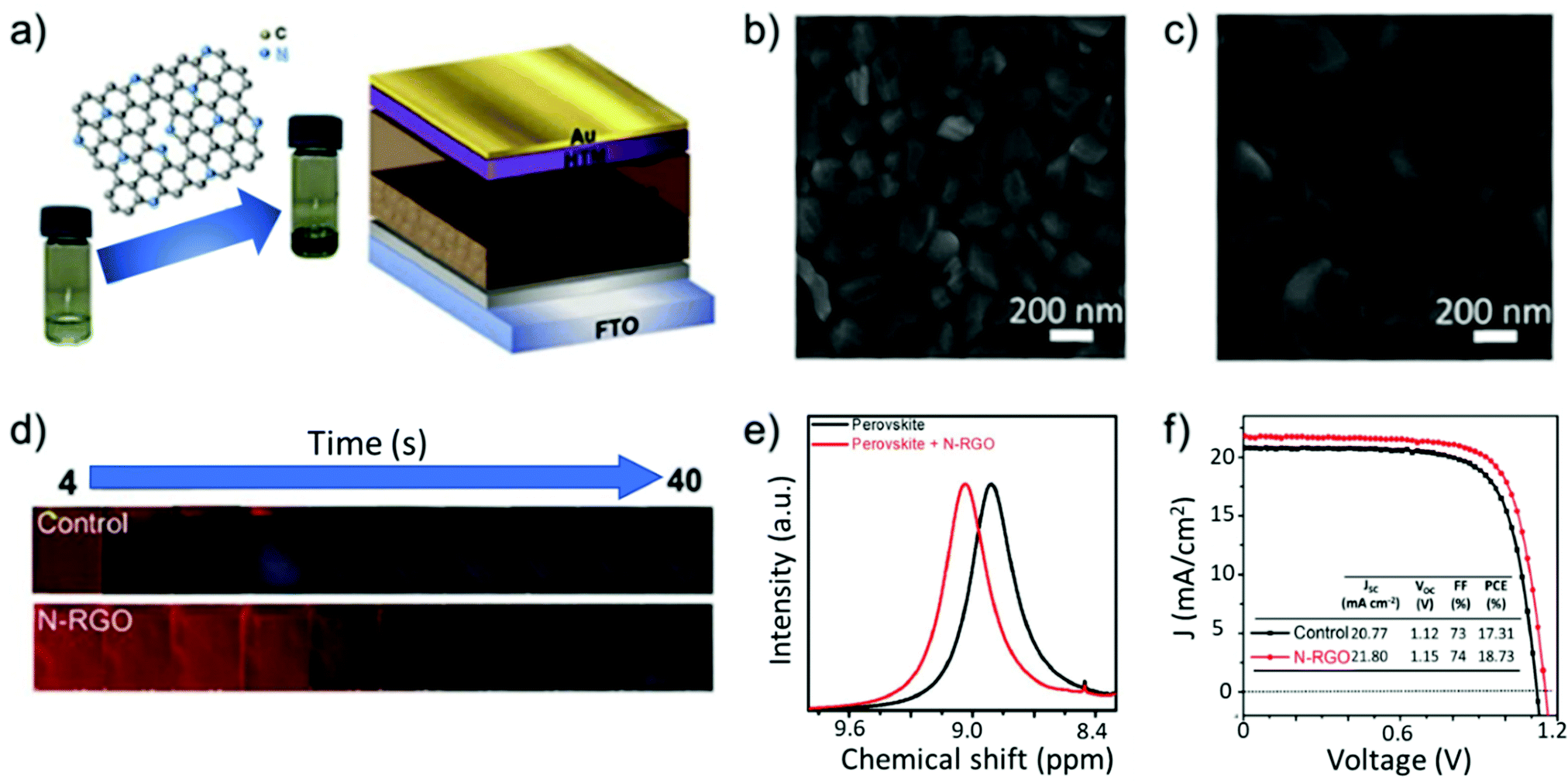 | ||
| Fig. 21 (a) Schematic showing the N-RGO-doped perovskite solution and PSC with a structure of FTO/TiO2/N-RGO/perovskite/spiro-OMeTAD/Au. (b and c) SEM images of perovskite films before and after the incorporation of N-RGO. (d) Photographs of perovskite films during the annealing process at 100 °C. (e) 1H NMR spectra of perovskite and N-RGO/perovskite solution. (f) J–V characteristics of the control device and N-RGO-incorporated device. Adapted from ref. 1134. | ||
The enhanced PV performance was attributed to the improved charge extraction and transport of MAPbI3 perovskite in the presence of BP nanosheets.1137 This approach was successfully applied to MAPbI3-based n–i–p1137 and p–i–n configurations,1138 demonstrating the maximum η value of 20.65% and 20.0%, respectively.
Moreover, the BP-doped n–i–p PSCs presented excellent photostability under prolonged light soaking, preserving 94% of the initial η after irradiation time of 1000 h,1137 while p–i–n PSCs have shown encouraging thermal stability, maintaining over 80% of their initial η value after aging for 100h at 100 °C.1139 As a further demonstration of the emergent role of BP in PSCs, X. Gong and co-workers demonstrated the use of BPQDs as an additive for inorganic CsPbI2Br perovskite films.1140 In that work, BPQDs were proposed as effective seed-like sites to modulate the nucleation and growth of CsPbI2Br perovskite crystals, affording device η above 15%.1139 Despite these results, the instability of few-layer phosphorene under ambient conditions1141 still represents a major concern hampering its massive use in PSCs.
In terms of the intrinsic stability of perovskites, Ag NP-anchored reduced graphene oxide (Ag-RGO) was used as an additive in perovskite films to suppress ion migration by improving the thermal and light stability.1142
Recently, Guo et al. used MXenes as a perovskite additive in mesoscopic PSCs.1143 In particular, the authors have shown that the termination groups of Ti3C2Tx can retard the perovskite crystallization rate, thereby increasing the perovskite crystal size.1142 After optimization, a 12% enhancement in η compared to the reference PSCs was obtained with 0.03 wt% MXenes.1142
Agresti et al. used Ti3C2 MXenes as perovskite WF modifier to design n–i–p mesoscopic devices with η exceeding 20%.1125 Density functional theory calculations demonstrated that the formation of an interface dipole at the perovskite/Ti3C2Tx interface strongly depends on Tx terminations.1125 For example, in the case of OH-terminated MXene, a larger interface dipole than O terminations was demonstrated.1125 The overall reduction in perovskite WF upon MXene addition and the optimization of MXene-based ETL led to a 26% increase in η, together with hysteresis reduction, compared with the reference cells without MXenes.1125 The possibility to vary the MXene WF on demand and control the band-energy alignments with other layers forming an electronic device represents a winning strategy to enlarge the design parameter space and improve the device performance.
The attempt from Hu et al. toward stabilizing the α-phase of Cs0.1FA0.9PbI3 perovskite by using 2D phenyl ethyl ammonium lead iodide ((PEA)2PbI4) nanosheets as the additive deserves a separate discussion, see Section 6.5.1144 Because of the 2D (PEA)2PbI4 nanosheets, the MA-free perovskite-based device reached a high η value of 20.44% and retained 82% of its initial efficiency after 800 h of continuous white light (1 sun) illumination.
Table 11 summarizes the main results achieved by PSCs integrating GRMs as perovskite additives.
| Material | Usage | Device structure | Cell perfomance | Ref. | |||
|---|---|---|---|---|---|---|---|
| J SC [mA cm−2] | V OC [V] | FF | η [%] | ||||
| a MA = CH3NH3. b FA = HC(NH2)2. | |||||||
| N-Doped RGO nanosheets | Additive in perovskite | (FTO)/cTiO2/mTiO2/FA0.85MA0.15Pb(I0.85Br0.15)3/spiro-OMeTAD/Au | 21.8 | 1.15 | 0.74 | 18.73 | 1134 |
| Graphene quantum dots (GQDs) | Additive for perovskite | FTO/cTiO2/mTiO2/MAPbI3/spiro-OMeTAD/Au | 22.91 | 1.05 | 0.76 | 18.34 | 1136 |
| 2D BP | Additive for perovskite | FTO/cTiO2/SnO2/perovskite:2D BP/Spiro-OMeTAD/Ag, | 1.82 | 23.31 | 0.82 | 20.65 | 1137 |
| Silver nanoparticle-anchored reduced graphene oxide (Ag-rGO) | Additive in perovskite | FTO/bl-TiO2/m-TiO2/Al2O3/MAPbI3−xClx/Ag-rGO/spiro-OMeTAD/Au | 0.929 | 23.501 | 0.74 | 16.101 | 1141 |
| Ti3C2 MXenes | Additive in perovskite | FTO/SnO2/MAPbI3:MXenes/spiro-OMeTAD/Au | 1.03 | 22.26 | 0.76 | 17.41 | 1142 |
| Ti3C2 (MXene) | ETL, interlayer at ETL/perovskite, additive in perovskite | FTO/cTiO2:MXenes/mTiO2:MXenes/Mxenes/Csx(MA0.17FA0.83)(1−x)Pb(I0.83Br0.17)3:MXenes/spiro-OMeTAD/Au | 1.09 | 23.82 | 0.78 | 20.14 | 675 |
| Black phosphorus quantum dots (BPQDs) | Additive in perovskite | ITO/PTAA/MAPbI3-BPQDs/PCBM/BCP/Ag | 21.9 | 1.10 | 0.83 | 20.0 | 1138 |
| BPQDs | Additive in perovskite | FTO/SnO2/BPQDs + CsPbI2Br/spiro-OMeTAD/Au | 15.86 | 1.25 | 0.78 | 15.47 | 1139 |
| 2D (PEA)2PbI4 nanosheets | Additive in perovskite | FTO/cTiO2/mTiO2/Cs0.1FA0.9PbI3 + 2D (PEA)2PbI4/spiro-OMeTAD/Au | 24.8 | 1.05 | 0.78 | 20.27 | 1143 |
| g-C3N4 | Additiver in perovskite | FTO/cTiO2/MAPbI3:g-C3N4/spiro-OMeTAD/Au | 24.31 | 1.07 | 0.74 | 19.49 | 282 |
6.3 HTLs and back electrodes
The main role of HTLs is to extract positive charges from the perovskite layer, by minimizing charge recombination losses, and to efficiently transport them at the corresponding current collector.1062,1063 Depending on the device's structure, HTLs have additional functions: in direct planar structures, HTLs also act as a perovskite protective layers against environmental factors (e.g., moisture and oxygen) and can even contribute to heat dissipation,1145,1146 improving the long-term stability of devices. In inverted planar structures, HTLs are often used as a scaffold layers for the growth of perovskites. Therefore, specific morphology and structural properties are required, especially for low-temperature solution-processed device fabrication on flexible substrates.1147 Moreover, because in such a configuration, sunlight comes from the p-type electrode, HTLs must be thin to prevent optical losses, while impeding short-circuiting between the conductive oxide (FTO or ITO for rigid and flexible substrates, respectively) and perovskite active layer.1148–1150 In addition, the HTLs need to ensure efficient hole transport toward the electrode by minimizing the series resistance, as well as charge recombination processes.1147–1149Finally, HTL-covered substrates should exhibit optimal wettability and compatibility with the solvent used for the perovskite deposition step. In this context, PEDOT:PSS has been the most frequently used HTL material in inverted PSCs, due to the following properties: (1) energy-level (HOMO level at 5.25 eV)1151 matching with ITO φW (4.9 eV)1152 and perovskite HOMO level (5.4 eV);1153 (2) excellent μ; (3) simple solution processability.1154 The doping with GRMs has been used to improve the physical, mechanical, and electrical features of PEDOT:PSS. For example, RGO was added into PEDOT:PSS.1155,1156 An η improvement of ∼22% was observed in RGO-doped PEDOT:PSS (RGO:PEDOT:PSS)-based device compared to the nondoped HTL-based reference due to the suppression of leakage current.1155 Giuri and co-workers investigated the cooperative effect of GO and glucose inclusion in the PEDOT:PSS matrix.1157 Chemically functionalized GO with the glucose molecule was used to modify the chemical properties of the PEDOT:PSS surface, changing the wettability, as well as improving the electrical conductivity of PEDOT:PSS.1156 Concurrently, glucose molecules favored the reduction of GO1158 and enhanced the wettability of the PEDOT:PSS substrate due to the presence of numerous hydroxyl terminations. Consequently, the GO-doped glucose/PEDOT:PSS HTL increased the VOC value compared to the PEDOT:PSS-based devices, indicating minimal losses, high hole selectivity, and reduced trap density at the optimized HTL/perovskite coverage.1156 The use of a chemical approach to control the optical and electrical properties of GO was also reported by Liu et al., who used silver trifluoromethanesulfonate (AgOTf) as an inorganic dopant for single-layer GO.1159 In particular, the spin coating of AgOTf in a nitromethane solution over a GO-doped PEDOT:PSS layer allowed the HTL φW to be finely tuned, thus lowering the energy barrier for hole transfer at the PEDOT:PSS:AgOTf-doped GO/perovskite interface.1158 This effect led to an η improvement for both flexible and rigid PSCs in comparison to the reference devices based on PEDOT:PSS.
Li et al. demonstrated that GO can also be used as an efficient interlayer between the conductive layer and PEDOT:PSS HTL.1160 In fact, the high conductivity of PEDOT:PSS combined with the electron-blocking capability of GO suppressed current leakage in the PSC structure, while improving the carrier injection and perovskite film morphology.1159 The as-realized device has shown a maximum η value of 13.1%, which was higher than that reached by the reference PSC based on PEDOT:PSS (η = 10%).1159
The insertion of a buffer layer between ITO and PEDOT:PSS has been demonstrated to significantly increase the long-term stability of nonencapsulated devices under atmospheric conditions (temperature of 21–24 °C and humidity of 38–55%).1058 In fact, the GO buffer layer can prohibit direct contact between the ITO and highly acidic PEDOT:PSS by slowing down photoelectrode degradation.1058 The improved η and stability achieved with 2D interlayers was clearly demonstrated by Kakavelakis and co-workers, who used a MoS2 interlayer between PTAA (HTL) and perovskite.1039 The introduction of MoS2 flakes afforded a device with an η value of 16.42% and a prolonged lifetime, corresponding to an 80% retention of their initial performance after 568 h of continuous illumination.1039 By following this approach, Tang and co-workers demonstrated planar inverted PSCs with the glass/ITO/PTAA/MoS2/perovskite/PCBM/BCP/Ag structure exceeding η of 20%.1161 In this case, the in-plane coupling between epitaxially grown CH3NH3PbI3 and MoS2 crystal lattices led to perovskite films with a large grain size, low trap density, and preferential growth orientation along the (110) direction normal to the MoS2 surface. Very recently, Zhang et al. replaced the MoS2 interlayer with 2D antimonene.1162 This new 2D material exhibits a thickness-dependent bandgap that can be advantageous in PV and other optoelectronic devices.1161 In particular, antimonene-based PSCs displayed an outstanding η value of 20.11% with a remarkable VOC value of 1.114 V, while the reference device has shown an η value of 17.60% with a VOC value of 1.065 V.1161 Antimonene provided sufficient nucleation sites, promoting perovskite crystallization and therefore speeding-up hole extraction at the photoelectrode.1161
Moreover, Cao et al. proposed the use of WS2 flakes as an efficient interlayer at the PTAA/perovskite interface, acting as a template for the van der Waals epitaxial growth of mixed perovskite films.1163 The WS2/perovskite heterojunction has shown an engineered energy alignment, boosting charge extraction and reducing interfacial recombination.1162 Inverted PSCs with WS2 interlayers reached η values up to 21.1%, which is among the highest value reported for inverted planar PSCs.1162 A further evolution in the use of 2D interlayers for planar PSCs was proposed by Wang and co-workers using a double interlayer approach: GO was used at the interface between PEDOT:PSS and perovskite, while MoS2 was used at the interface between PCBM and the Ag electrode.1164 The PSC with GO and MoS2 layers has shown an increase in VOC from 0.962 to 1.135 V, and η from 14.15% to 19.14%.1163 However, despite the extensive use of PEDOT:PSS in PSCs, PEDOT:PSS suffers from hygroscopicity and acidic properties, which cause faster degradation of both organic layers and organolead halide perovskites layer.1165 Thus, several efforts have been made in order to replace PEDOT:PSS with the most stable HTL based on graphene or other 2D materials, including TMDs.1166,1167 In fact, the lone pair of electrons of the carbon and chalcogen atoms in the structure of graphene (and derivative) and TMDs, respectively, improves the μ value of HTL, due to the demonstrated ballistic transport.1168–1170 Moreover, chemical doping and simple surface treatment allow the easy modulation of the energy levels of both (R)GO1171,1172 and TMD films.1173,1174 For example, Kim and co-workers demonstrated the feasibility to replace PEDOT:PSS with polycrystalline structure of MoS2 and WS2 layers, which were synthesized through a chemical deposition method.1150 The devices with a planar inverted architecture of ITO/MoS2 or WS2/perovskite/PCBM/BCO/LiF/Al exhibited η of 9.53% and 8.02% for MoS2 and WS2 cases, respectively, comparable to that measured for PEDOT:PSS-based devices (9.93%).1150 In the same work, the use of GO as the HTL resulted in an η of 9.62%, demonstrating the effectiveness of GRMs in PSCs.1150 The use of TMDs for HTL in inverted PSCs has been recently optimized by Huang and co-workers, who achieved an η of 14.35% and 15.00% for MoS2- and WS2-based PSCs, also demonstrating enhanced stability compared to the PEDOT:PSS-based reference devices.1175
Following the aforementioned studies, GO and RGO in both pristine and functionalized forms have been extensively tested as HTLs, yielding valuable results in terms of η and stability. For example, Wu et al. improved the η of ITO/HTL/CH3NH3PbI3−xClx/PCBM/ZnO/Al PSCs from 9.2% to 12.4% by replacing PEDOT:PSS with a GO layer.1050 In particular, by tuning the concentrations of GO in neutral aqueous suspensions from 0.25 mg mL−1 to 4 mg mL−1, the authors were able to deposit a GO layer with a thickness in the range of ∼2–20 nm, finely controlling the PV performance of the devices.1050
More recently, GO has been exploited as the HTM even in the form of nitrogen-doped nanoribbons (NGONRs) by Kim and co-workers.1176 The NGONRs were synthetized starting from MWCNTs and subsequently doped by pyrolyzing nanoribbons/polyaniline (PANI) composites at 900 °C for 1 h in an Ar atmosphere.1175 Different from the case of PEDOT:PSS, the deposition of perovskite films onto NGONRs allowed the perovskite film to grow into large textured domains, yielding an almost complete coverage.1175 Thus, small-area devices reached an η value of 12.41%, which was higher than that of the PEDOT:PSS-based reference (9.70%).1175 Notably, NGONR-based cells demonstrated negligible current hysteresis along with improved stability under ambient conditions (average temperature and humidity of 20 °C and 47%, respectively), since the absence of the PEDOT:PSS layer prevented perovskite degradation caused by the acidic nature of the polymer.1175 A significant η of 16.5% and extraordinary stability was also achieved by using GO as the HTL in an inverted PSC.1177 Long-term aging test under ambient humidity with a relative humidity of 60% was carried out on the encapsulated devices.1176 After initial J–V measurements, the devices were continuously illuminated and then stored in the dark under standard laboratory conditions.1176 The GO-based devices reported long-term stability compared to PEDOT:PSS-based PSCs.1176 In particular, their η decreased by only 10% after nearly 2000 h.1176
The improvement in device stability was demonstrated using a RGO nanosheet as the HTL in the inverted structure of ITO/RGO/perovskite/PCBM/BCP/Ag.1049 The RGO/perovskite junction induced faster charge transfer across its interface, resulting in reduced charge recombination compared to the PEDOT:PSS-based PSCs.1049 Furthermore, the perovskite grains (100–200 nm grains) of the perovskite film grown on the RGO layer reduced the total number of grain boundaries, increasing the cell FF, compared to the PEDOT:PSS-based reference (perovskite with grain size of <100 nm).1049 RGO-based devices have shown promising stability, retaining 62% of the initial η even after 140 h of light exposure, while PEDOT-PSS-based devices failed.1049 The stability of cells with RGO stemmed from the quasi-neutral properties of RGO with few surface oxygen functionalities and the inherent passivation ability of RGO against moisture and oxygen.1049 With the aim to further enhance the stability of PEDOT:PSS-based inverted PSCs, GO1178 and ammonia-modified GO (GO:NH3)1179 were reported as efficient interlayers between the HTL and perovskite active layer. In the latter case, a thin GO:NH3 layer of ∼2 nm was spin coated onto the PEDOT:PSS surface and subsequently annealed at 120 °C for 10 min.1178 Similar to the results reported using the RGO nanosheet,1049 the perovskite film realized onto the PEDOT:PSS/GO:NH3 substrate displayed improved crystallization with a preferred orientation order and nearly complete coverage, improving its optical absorption.1178 Furthermore, the optimal energy-level matching between the PEDOT:PSS-GO:NH3 HTL and perovskite led to an η value up to 16.11%, which was significantly superior compared to the values measured for bare PEDOT:PSS-based PSCs (η = 12.5%).1178 Notably, the highly ordered perovskite structure led to a marked improvement in the structural stability of the active film, extending the device lifetime in ambient conditions.1178 Organo-sulfonate graphene (oxo-G) was reported to replace PEDOT:PSS in inverted PSCs, significantly enlarging the device's lifetime.1180 In fact, the use of oxo-G as the HTL effectively prevented the access of water vapor into the device stack, without penalizing the overall η of the devices, which reached valuable η of 15.6%.1179 Noteworthily, the unencapsulated devices retained ∼60% of the initial η after ∼1000 h light soaking under 0.5 sun and ambient condition.1179 The obtained results confirmed the use of functionalized graphene-based materials as a viable route to stabilize inverted PSCs.1179
In the archetypical mesoscopic structure of cTiO2/mTiO2 (or Al2O3)/perovskite/spiro-OMeOTAD/Au, GRMs have been widely used to replace traditional HTMs, as well as interlayers, mainly aiming to solve certain issues related to the spiro-OMeOTAD HTL, such as instability and high cost ($170–475/g).1181 In particular, spiro-OMeTAD needs to be doped to increase the intrinsic low electrical conductivity of its pristine amorphous form.1182 To this end, lithium bis(trifluoromethanesulfonyl)imide (Li-TFSI)1183,1184 and tert-butylpyridine (TBP)1185 are the most frequently used dopants to increase μh and to improve contact at the spiro-OMeTAD/perovskite interface, respectively. However, major instability drawbacks must be considered when the aforementioned dopants are used. In fact, Li-TFSI exposed to ambient conditions is deliquescent1186 and tends to dissociate from the spiro-OMeTAD, negatively affecting its performances.1185 In addition, TBP corrodes the perovskite layer due to its polar nature.1187
With the aim to replace common dopants of the spiro-OMeTAD layer, Luo and co-authors recently proposed the use of GO reduced by a ferrous iodide acidic solution as an alternative HTM dopant.1188 The devices prepared using iodine-RGO/spiro-OMeTAD HTL displayed an η of 10.6%, which was lower compared to that of doped spiro-OMeTAD-based devices (13.01%).1187 However, the cell stability was significantly improved.1187 In particular, the η value of the RGO-based devices retained above 85% of the initial value even after 500 h of storage in air, while the η value of the device fabricated with doped spiro-OMeTAD decreased to 35% under the same aging conditions.1187
An alternative strategy to enhance cell η by preventing perovskite/spiro-OMeTAD interface degradation involves the use of an interfacial layer based on 2D materials. As a recent example, phosphorene has been used at both mTiO2/perovskite and perovskite/spiro-OMeTAD interfaces in mesoscopic n–i–p PSCs, achieving a remarkable η of 19.83%.
Solution-processed phosphorene has shown ambipolar carrier transport behavior and can be considered as a viable route for enabling great advances in PSC performance via judicious interfacial positioning of phosphorene in the cell structure.1189 Regarding the perovskite/spiro-OMeTAD interface stability, Capasso et al. showed that the insertion of few-layers MoS2 retarded PSC degradation with higher lifetime stability, of over 550 h, compared to the reference MoS2-free PSC (Δη/η = −7% vs. Δη/η = −34%).1190 The authors justified the extended lifetime to the role of MoS2 flakes that act as a protective layer, preventing the formation of shunt contacts between the perovskite and Au electrode.1189 The enhanced stability of the mesoscopic device using an MoS2 interlayer was recently demonstrated even under prolonged light soaking condition at 1 sun illumination.1105,1191 However, the MoS2 VB does not perfectly match with the perovskite HOMO level, possibly forming an energy barrier for the hole extraction process that causes VOC reduction. In order to fully exploit the potential of MoS2 as an interlayer, Najafi et al. produced MoS2 quantum dots (MoS2 QDs), derived by LPE-produced MoS2 flakes and hybridized with functionalized reduced graphene oxide (f-RGO), to provide both hole extraction and electron blocking properties (Fig. 22).1192 In fact, the intrinsic n-type doping of the MoS2 flakes introduce intraband gap states that can extract holes through an electron injection mechanism.1191 Meanwhile, quantum confinement effects increase the Eg of MoS2 (from 1.4 eV for flakes to more than 3.2 eV for QDs), rising its CB minimum energy from −4.3 eV to −2.2 eV. The latter value is above the CB of CH3NH3PbI3. Therefore MoS2 QDs exhibit electron-blocking properties.1191 In addition, the hybridization of MoS2 QDs with f-RGO, obtained by chemical silanization-induced linkage between RGO and (3-mercaptopropyl)trimethoxysilane, promoting the deposition of a homogeneous interlayer onto the perovskite film.1191 In fact, the f-RGO flakes plug the pinholes of MoS2 QD films.1191 The as-prepared PSCs achieved η values of up to 20.12% (average η of 18.8%).1191 As an alternative to MoS2 QDs, Agresti et al. proposed a chemical functionalization of the MoS2 flakes (fMoS2), by linking a thiol group of 3-mercaptopropionic acid (MPA) moieties to the MoS2 surface via S–S van der Waals physisorption and/or S-vacancy passivation (Fig. 23).1193 Apart from chemically and electronically repairing the defective lattice of the MoS2 flakes, MPA-based functionalization is effective to upshift the MoS2 energy bands.1192 The upshift of the MoS2 energy bands aligns the VB edge of MoS2 with the HOMO level of the perovskite, improving the hole extraction process.1192 In addition, the MPA-based functionalization shifts the CB edge of MoS2 above the LUMO level of the perovskite, hindering undesired electron transfer (i.e., providing electron blocking properties).1192 Owing to these effects, the MPA-based functionalization of MoS2 flakes, when integrated in PSCs, improved the η value of the reference devices without MoS2-based interlayer by +11.6%.1192
 | ||
| Fig. 22 (a) Schematic of mesoscopic MAPbI3-based PSC using MoS2 QDs:f-RGO hybrids as both HTL and active buffer layer. (b) Schematic of the energy band edge positions of the materials used in different components of the assembled mesoscopic MAPbI3-based PSCs. Reprinted with permission from ref. 1191, Copyright 2018, American Chemical Society. | ||
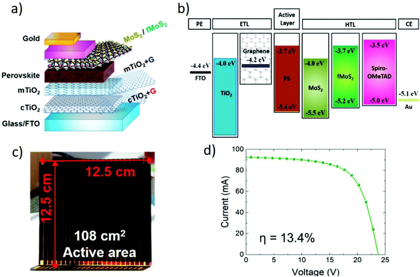 | ||
| Fig. 23 (a) Engineered PSC architecture using chemically functionalized molybdenum disulfide (fMoS2) as the interlayer at the perovskite/HTL interface for improving the hole injection/collection at the CE and (b) its energy band diagram. (c) Photograph of a representative large-area PSM (108 cm2 active area, 156.25 cm2 substrate area), showing an η value of 13.4% under 1 sun illumination, as shown by (d) its J–V characteristic. Adapted with permission from ref. 1192, Copyright 2019, American Chemical Society. | ||
Recently, another mechanism has been proposed by Shi et al. to explain the hole extraction properties of 2D MoS2.1194 This mechanism relies on the presence of intrinsic S vacancies at the MoS2 edges that stabilize halide vacancies at the perovskite/MoS2 interface.1193 This process induces an interface dipole moment, which reverses the offset of the VB maxima.1193 Overall, this effect can lead to an ultrafast (picosecond timescale) hole transport from the perovskite to the current collector, boosting the performance of MoS2 HTL-based PSCs.
Beyond MoS2, both GO1195 and functionalized GO (fGO)1196 were used as an efficient buffer layer at the perovskite/spiro-OMeTAD interface. In particular, when GO was deposited onto the perovskite surface, it performed as a base that absorbed spiro-OMeTAD onto its surface.1194 Moreover, parts of the O atoms in GO were demonstrated to connect with unsaturated Pb atoms in the perovskite, improving adhesion between spiro-OMeTAD and the active layer.1194 Furthermore, the surface defect states of the perovskite were dramatically reduced, leading to an η increase of 45.5%, from 10.0% in the case of a standard PSC structure to 14.5% when GO was inserted as the interlayer.1194
Amino-functionalized N-doped graphene (NG) was tested as an interlayer between perovskite and undoped spiro-OMeTAD in the standard mesoscopic structure (FTO/cTiO2/mTiO2/perovskite/dopant-free spiro-OMeTAD/Au), reaching higher η (14.6%) compared to the reference device (η = 10.7%).1195 These results were explained by the absorption of spiro-OMeTAD from NG-treated perovskite surface via π–π interactions, ensuring electron-rich molecules. In fact, N atoms interact with undercoordinated Pb2+ ions by donating electron density.1195 Thus, the perovskite surface is passivated and the charge extraction toward the HTL is optimized.1195,1197 Consequently, η enhancement was associated with the increase in JSC and FF due to reduced charge recombination at the perovskite/HTM interface.1195 Functionalized RGO was also used at the perovskite/spiro-OMeTAD interface in the planar configuration to reduce interfacial recombination and enhance hole extraction.1198 An alternative strategy to replace spiro-OMeTAD is to use more stable and dopant-free HTMs. To this end, Nouri et al. demonstrated that the use of copper phthalocyanine (CPC) as an alternative HTM can produce valuable η only if an interlayer of GO was used between the perovskite and HTL.1199 In a recent work, You et al. proposed the use of solution-processed high-mobility 2D materials, namely, MoS2 and BP, to conduct holes from the grain boundary of the perovskite layer to the HTL, proposing a novel strategy to passivate defects in PSC grain boundaries.1200
An attempt to replace spiro-OMeTAD with sprayed RGO was reported by Palma et al.1052 Despite the η values of RGO-based PSCs (η = 5%) were lower than that obtained with devices based on doped spiro-OMeTAD as the HTL (η = 11%), the authors have reported an impressive improvement in device stability.1052 In fact, PSC stability was demonstrated in an endurance test carried out under both shelf-life conditions (in air, in dark, at ambient temperature (RT = 23 °C) and relative humidity (RH = 50%)) and open-circuit load conditions for prolonged light-soaking stress test (1 sun at 65 °C and ambient RH).1052 In particular, 1987 h of shelf-life testing revealed that η increased by more than 30% in RGO-based-PSCs, while spiro-OMETAD-based PSCs evidenced a drastic η reduction (–44%).1052 Notably, the consecutive light-soaking tests induced a further η decrease of only 26% in RGO-based PSCs, while spiro-OMeTAD-based device completely failed the test.1052
RGO was also used as a dopant for poly-3(hexylthiophene) (P3HT) polymer, a valid HTM alternative to spiro-OMeTAD when doped with LiTFSI salts and TBP.1201 The enhanced η (∼9%) of PSC using RGO-doped P3HT compared to devices using bare P3HT (6.5%) was complemented by improved shelf-life stability.1200 The authors demonstrated that RGO doping introduced additional charge percolation pathways in P3HT and enhanced the interfacial contacts with the underlying perovskite layer and Au back electrode.1200 Thus, improved hole depletion from the perovskite layer limits charge recombination effects by avoiding trapped charges at the perovskite/HTM interface.1202 The increase in μh of P3HT was reported as the key point to improve the PSC performance by Ye and co-workers, who proposed an imidazole-functionalized GO (IGO) as the HTL dopant.1053 PSCs using IGO-doped P3HT achieved an η value of 13.82%, which was among the highest reported for P3HT-based PSCs.1053 Apart from the increase in μh, IGO doping allowed the P3HT HOMO level to be shifted from −5.0 eV to −5.2 eV.1053 Moreover, the hydrophobicity of the P3HT/graphene layer resulted in excellent stability of the PSCs, which retained more than 70% of their initial performance after 8 weeks of storage in ambient conditions (25 °C, 20–40% RH).1053
The hydrophobicity of GRMs is a peculiar property that drives their exploitation in the development of new and more robust HTMs and/or protecting layers for PSCs. Very recently, Cao and co-workers successfully replaced spiro-OMeTAD with a perthiolated tri-sulfur-annulated hexa-peri-hexabenzocoronene (TSHBC)/graphene layer, achieving an η value exceeding 14% on small-area devices.1055 Such a tested compound combined the hydrophobicity of both graphenes and thiols, providing an effective molecular sealing approach to improve the stability of complete devices.1055 Moreover, the TSHBC/graphene layer exhibited an excellent hole extraction capability, ensuing from the Pb–S coordination bond between TSHBC and perovskite, together with enhanced μh due to the presence of GNSs in the HTL.1055 A similar approach was also reported by Wang and co-authors that used a multilayered buffer layer with the aim to replace spiro-OMeTAD and to protect perovskite from moisture.1056 The realized SWNT/GO/polymethyl methacrylate (PMMA) layer conjugated the SWNT capability in assisting photogenerated carrier extraction/transport with the electron blocking property of GO.1056 Moreover, the built-in potential across the device drastically increased upon the insertion of the GO layer, which prevented carrier recombination losses.1056 With regard to stability, the η of spiro-OMeTAD-based PSC significantly reduced from 10.5% to 5.8% during a ten-day test, while the SWNT/GO/PMMA-based cells exhibited stable performance, showing a decrease of η from 10.5% to 10.0% in the same timeframe.1056 This result was attributed to the PMMA layer, which acts as an effective barrier to moisture and oxygen penetration, preventing the degradation of the perovskite layer.1056 We should mention that HTM doping was also realized using 2D materials other than GO.1203 Indeed, effective HTMs were produced by means of BP,1204,1205 graphene,1206 and functionalized MoS21207 dopants. For example, BP/spiro-OMeTAD blend-based PSCs have shown a remarkable increase in η (more than 20%) compared to PSCs without BP.1203 Lastly, solution-processed 2D-conjugated polymers have also been proposed as effective dopant-free HTL materials alternative to spiro-OMeTAD, confirming that the design of novel 2D materials can prospectively offer advanced strategies to further boost the η and the stability of PSCs.1208 In detail, planar n–i–p-structured PSCs based on 2DP-TDB as a dopant-free HTM recently achieved champion η as high as 22.17%, while showing improved stability under continuous light soaking in an inert atmosphere compared to control devices.1207
Recently, graphene-based dopants for HTLs have been demonstrated to have a crucial role in CE replacement.1209 In fact, one of the main hurdles of PSC technology is that the hole transporting materials established for state-of-the art Au-based devices are not compatible with carbon pastes used for the fabrication of carbon-based PSCs. Thus, Chu et al. proposed the use of HTL based on solution-processed P3HT/graphene composites, exhibiting outstanding μh and thermal tolerance.1208 In fact, after annealing at 100 °C, the μh value of this HTL increased from 8.3 × 10⁻³ to 1.2 × 10⁻² cm2 V−1 s−1, which was two orders of magnitude larger than that of pure P3HT.1208 As a result, the authors reported carbon-based PSCs with a record η value of 17.8% (certified by Newport).1208 This cell was the first PSC to be certified under a stabilized testing protocol.1208 The P3HT/graphene composite-based HTL device yielded a champion device with η of 18.2%.1208 In comparison, the use of sole P3HT as the HTL resulted in a device with inferior performance, i.e., η = 11.1%.1208 The outstanding stability of a unencapsulated device based on P3HT/graphene HTL was demonstrated by only 3% drop after 1680 h storage in ambient conditions with a relative humidity of ∼50%.1208 After encapsulation, the device retained ∼89% of its initial η under continuous 1 sun illumination at RT for 600 h in a N2 environment.1208 In comparison, the device using P3HT HTL exhibited rapid degradation, reaching ∼25% of its original η after ∼75 h.1208 Device stability improvement using GRMs was also demonstrated by Bi and co-workers using a nanostructured carbon layer into the device structure.1210 In particular, an ETL based on PCBM containing N-doped graphene coupled with a carbon quantum dot (CQD) interlayer before Ag CE effectively suppressed the diffusion of ions/molecules within PSCs, preventing perovskite degradation.1209 In fact, the stable η of a CQDs/G-PCBM-based device over 15% was measured when the device was kept in the dark at RT for 5000 h or under AM 1.5G simulated solar light for 1000 h.1209 In particular, during the thermal aging test at 85 °C for 500 h, the devices retained 98% of the initial η.1209
Aurora et al. recently reported a breakthrough in the race for the design and realization of stable PSCs.1038 The authors demonstrated the possible replacement of expensive spiro-OMeTAD with CuSCN as the HTL by achieving a remarkable η above 20%.1038 The addition of a conductive RGO spacer layer between CuSCN and Au allowed the PSCs to retain more than 95% of the initial η after aging at MPP for 1000 h under 1 sun illumination at 60 °C (Fig. 24).1038
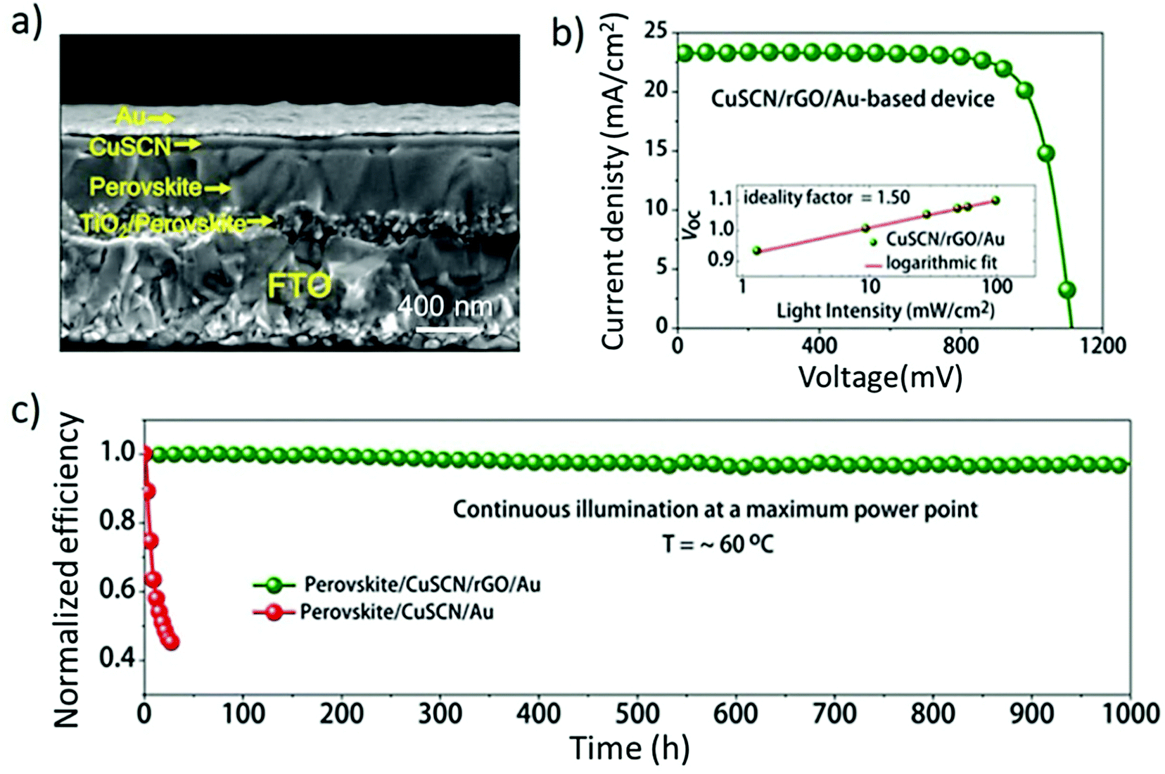 | ||
| Fig. 24 (a) Cross-sectional SEM micrograph displaying the thickness of different layers in a complete mesoscopic n–i–p PSC employing rGO as the buffer layer between CuSCN-based HTL and Au CE, (b) J–V curve of the CuSCN-based device showing η = 20.4%; the inset shows VOC as a function of illumination intensity with an ideality factor of 1.50. (c) Stabilities of an unencapsulated device based on CuSCN HTL and an unencapsulated CuSCN-based device incorporating a thin layer of RGO between the Au and CuSCN layers, evaluated at the MPPs under continuous simulated sunlight illumination at 60 °C in a N2 atmosphere. Adapted from ref. 1038. | ||
Graphene was demonstrated to play a major role in reducing the high sheet resistance of PEDOT:PSS used in form of adhesive CEs.1211 In fact, PEDOT:PSS was easily spin coated on graphene/PMMA/poly(dimethylsiloxane) (PDMS) substrates to realize the CE, which was subsequently laminated on the perovskite substrate.1210 When 4-layer graphene was embedded in the CE, a remarkable η value of 12.4% was achieved under light illumination from the FTO side, while device semitransparency was demonstrated by reporting an η of 4.37% during illumination from the CE side.1210 However, this work was conducted using CVD graphene, and a similar approach based on solution-processed graphene must be consolidated. Notably, the number of graphene layers was key for the device performance optimization.1210 In fact, even though a large number of layers decreases the series resistance, a number of graphene layers higher than 5 compromises the adhesion between graphene and spiro-OMeTAD.1210
An effective approach to improve PSC stability is represented by the replacement of the metal CE with a carbon-based back electrode, to form the so-called carbon perovskite solar cells (C-PSCs).1212–1219 In fact, Au is a well-known cause of instability, since it suffers from metal-ion migration phenomenon degrading the perovskite and HTLs when the device experiences an operating temperature above 70 °C.1220 So far, three types of C-PSCs have been proposed, namely, mesoporous,1221 embedment,1222–1224 and paintable C-PSCs.1125,1126,1225 In mesoporous C-PSCs, a porous carbon electrode is first deposited and then the perovskite is infiltrated within it to complete the structure.1218,1220 To produce embedment C-PSCs, a porous carbon electrode is deposited onto a perovskite precursor (e.g., PbI2), followed by the conversion of the precursor to perovskite by infiltrating a reaction solution.1221–1223 Lastly, the carbon CE can be directly deposited onto the perovskite layer, HTL, or ETL depending on the device configuration (i.e., CTL-free devices, n–i–p, and p–i–n configurations, respectively) to obtain paintable C-PSCs. Recent reviews on C-PSCs summarized the advantages of such technology compared to conventional PSCs,1211–1217 including low cost, chemical inertness of the carbon-based material to halide ions, and hydrophobic characteristics. Therefore, we refer the reader to these earlier reviews, while, here, we will specifically focus on the progresses achieved in C-PSCs by using solution-processed 2D materials. In particular, Grancini et al. used a 2D/3D (HOOC(CH2)4NH3)2PbI4/CH3NH3PbI3 perovskite junction as the active layer to develop 10 × 10cm2 solar modules by a fully printable industrial-scale process, delivering a stable η value of 11.2% for more than 10000 h with zero loss in performance measured under controlled standard conditions.1218 However, due to poor perovskite layer uniformity, the perovskite infiltration process still represents a critical step, and a facile carbon paste deposition process onto the perovskite is highly pursued. For this purpose, Chen et al. recently applied carbon CE over all-inorganic PSCs based on a CsPbBr3 absorber.1227 In this work, Ti3C2-MXene nanosheets were used as the interlayer to eliminate energy-level mismatches, accelerate hole extraction, and reduce the recombination at the interface of perovskite/carbon electrode.1226 Following this approach, PSCs showing an initial η of 9.0% and long-term stability in a moisture environment over 1900 h (over 600 h under thermal conditions) have been demonstrated.1226 As alternatives to conventional carbon paste, SLG, FLG, and multilayer graphene (MLG) have been reported for the realization of metal-free CEs in mesoscopic PSCs.1228 In particular, an η value of 11.5% was achieved using reduced multilayered graphene oxide (MGO) at 1000 °C under an Ar atmosphere.1227 In comparison to SLG, the better hole extraction of MGO was ascribed to the as-formed Schottky barrier,1227 while an ohmic contact was established for the case of SLG.1227 Furthermore, larger transport coefficient, longer photocarrier lifetime, and twice the diffusion length have been demonstrated for MGO in comparison with SLG, opening a new route toward the low-cost production of Au-free PSCs.1227 N-Doped graphene frameworks (N-GFs), forming covalently bonded 3D structures, were also used as excellent CEs in HTL-free PSCs, achieving an η of 10.32%.1229
Recently, Mariani et al. reported low-temperature graphene-based carbon pastes in alcoholic solvents compatible with prototypical PSC materials used in standard configurations, namely, the triple cation Cs0.05(FA0.85MA0.15)0.95Pb(I0.85Br0.15)3 perovskite and spiro-OMeTAD HTL.1230 The corresponding graphene-based CEs have been applied to large-area (1 cm2) mesoscopic devices and low-temperature-processed planar n–i–p devices that reached η values of 13.85% and 14.06%, respectively.1229 Moreover, proof-of-concept metallized mini-wafer-like C-PSCs over a substrate area of 6.76 cm2 (aperture area = 4.00 cm2) afforded an η of 13.86%, which corresponded to a record-high η value of 12.10% on the aperture area. These results proved, for the first time, the metallization compatibility with such paintable C-PSC configurations.1229
Carbon back electrode mechanically stacked with another carbon-coated FTO glass under pressure was also proposed to realize an innovative modular flexible C-PSC design.1231 Among the different carbon nanomaterials (i.e., carbon black, graphite sheet, and RGO), RGO has shown η as high as 18.65%, which was the record-high value reported for C-PSCs.1230 Furthermore, graphene-based C-PSCs retained 90% of their initial η after aging at an elevated temperature of 85 °C for 1000 h without any encapsulation.1230 Very recently, Ti3C2 MXenes have been used as the back electrode for mesoscopic n–i–p PSCs in HTL-free configurations. In particular, Ti3C2 has been directly deposited over a MAPbI3 perovskite layer by doctor-blade coating1232 or alternatively by using a simple hot-pressing method.1233 Despite the highest η value for PSCs using MXene-based back electrode was 13.83%, the as-produced devices have shown improved stability in the ambient atmosphere at RT (humidity: 30%) compared to gold-based PSCs.1232Table 12 summarizes the main results achieved by PSCs using HTLs and back electrodes based on GRMs.
| Material | Usage | Device structure | Cell perfomance | Ref. | |||
|---|---|---|---|---|---|---|---|
| J SC [mA cm−2] | V OC [V] | FF | η [%] | ||||
| a MA = CH3NH3. b FA = HC(NH2)2. | |||||||
| (a) GO or (b) WS2 or (c) MoS2 | HTL | ITO/GO or WS2 or MoS2/MAPbI3−xClx/PCBM/BCO/LiF/Al | (a) 14.51 | (a) 0.92 | (a) 0.72 | (a) 9.62 | 1150 |
| (b) 15.91 | (b) 0.82 | (b) 0.64 | (b) 8.02 | ||||
| (c) 14.89 | (c) 0.96 | (c) 0.67 | (c) 9.53 | ||||
| RGO | Dopant for HTL | ITO/RGO-PEDOT:PSS/MAPbI3/PC61BM/Al | 17.1 | 0.95 | 0.64 | 10.6 | 1155 |
| GO | Dopant for HTL | ITO/PEDOT:PSS:GO:glucose/MAPbI3/PC61BM/LiF/Al | 17.6 | 1.05 | 0.69 | 12.8 | 1156 |
| AgOTf-doped GO | Dopant for HTL | ITO/PEDOT:PSS:AgOTf-doped GO/MAPbI3−xClx/PCBM/Au | 19.18 | 0.88 | 0.7 | 11.9 | 1158 |
| GO | Interlayer at front electrode/HTL interface | ITO/GO/PEDOT:PSS/MAPbI3/PC61BM/Al | 17.96 | 0.96 | 0.76 | 13.1 | 1159 |
| GO | HTL | ITO/GO/MAPbI3−xClx/PC61BM/ZnO/Al | 15.59 | 0.99 | 0.72 | 11.11 | 1050 |
| NGONRs | HTL | FTO/NGONR/MAPbI3/ZnO NPs/Al. | 17.93 | 1.00 | 0.72 | 12.94 | 1175 |
| Ammonia modified GO (GO:NH3) | Interlayer at HTL/perovskite interface | ITO/PEDOT:PSS-GO:NH3/MAPbI3−xClx/PC61BM/Bphen/Ag. | 22.06 | 1.03 | 0.71 | 16.11 | 1178 |
| Organosulfate-G (oxo-G) | HTL | Oxo-G1/MAPbI3/PC61BM/Zn/Al | 18.06 | 1.08 | 0.78 | 15.2 | 1179 |
| GO | Interlayer at HTL/perovskite interface | FTO/cTiO2/mTiO2/MAPbI3/GO/spiro-OMeTAD/Au | 20.2 | 1-04 | 0.73 | 15.1 | 1186 |
| Iodine reduced GO | Dopant for HTL | FTO/cTiO2/mTiO2/MAPbI3/GO/spiro-OMeTAD/Au | 19.6 | 1.00 | 0.68 | 13.33 | 1187 |
| MoS2 | Interlayer at HTL/perovskite interface | FTO/c TiO2/mTiO2/MAPbI3/MoS2/spiro-OMeTAD/Au | 21.5 | 0.93 | 0.67 | 13.3 | 1192 |
| Amino-functionalized GO (NGO) | Interlayer at HTL/perovskite interface | FTO/c TiO2/mTiO2/MAPbI3/NGO/spiro-OMeTAD/Au | 23.6 | 0.94 | 0.66 | 14.6 | 1195 |
| (p-Methoxyphenyl -single walled carbon nonotube) SWCNT-PhOMe and RGO | Dopants for HTL | FTO/cTiO2/mTiO2/MAPbI3/P3HT:SWCNT-PhOMe:RGO)/Au | 18.8 | 0.87 | 0.62 | 10.0 | 1200 |
| (a) (SLG) or (b) MLG | HTL and back electrode | (a) FTO/cTiO2/mTiO2/MAPbI3/SLG (b) FTO/cTiO2/mTiO2/MAPbI3/MLG | (a) 14.2 | (a) 0.88 | (a) 0.54 | (a) 6.7 | 1227 |
| (b) 16.7 | (b) 0.94 | (b) 0.73 | (b) 11.5 | ||||
| RGO | Interlayer at HTL/back electrode interface | FTO/TiO2/CsFAMAPbI3–xBrx/CuSCN/RGO/Au | 23.24 | 1.112 | 0.782 | 20.4 | 1038 |
| MoS2 | Interlayer at HTL/perovskite | ITO/PTAA/MoS2/MAPbI3−xClx/PCBM/PFN/Al. | 20.71 | 1.011 | 0.784 | 16.89 | 1039 |
| Black phosporous (BP) nanosheets | HTL | FTO/TiO2/MAPbI3/(spiro-OMeTAD:BP nanosheets)/Au | 20.22 | 1.06 | 0.761 | 16.4 | 1203 |
| Black phosphorous QDs (BPQDs) | Interlayer at HTL/perovskite | ITO/(PEDOT:PSS:PBQDs)/MAPbI3/ZrAcAc-modified PCBM/Ag | 20.56 | 1.01 | 80.0 | 16.69 | 1204 |
| Ti3C2 MXenes | Interlayer at perovskite/CE interface | FTO/TiO2/CsPbBr3/MXenes/Carbon | 8.54 | 1.44 | 0.73 | 9.01 | 1226 |
| Graphene | HTL | FTO/TiO2/FAMAPbI3/(PEDOT:graphene)/Au | 21.32 | 0.79 | 0.518 | 8.79 | 1205 |
| Graphene | HTL | FTO/TiO2/(FAPbI3)0.85(MAPbBr3)0.15/(PTh:graphene)/Au | 20.07 | 0.57 | 0.43 | 4.95 | 1205 |
| Phenyl acetylene silver (PAS)-functionalized MoS2 | Dopant for HTL | FTO/(PEDOT:PSS:MoS2)/MAPbI3/PCBM/Ag | 24.035 | 0.998 | 0.686 | 16.47 | 1206 |
| RGO functionalized with 4-fluorophenyl-hydrazine hydrochloride (4FPH) | Interlayer at HTL/perovskite interface | ITO/TiO2/MAPbI3Cl3−x/RGO-4FPH/spiro-OMeTAD/Au | 21.5 | 1.11 | 0.786 | 18.75 | 1197 |
| GO | Dopant for HTL | ITO/GO-doped PEDOT:PSS/(FAPbI3)0.85(MAPbBr3)0.15/PC61BM/BCP/Ag | 20.01 | 0.90 | 0.79 | 14.20 | 1202 |
| GO | Interlayer at HTL/perovskite interface | FTO/TiO2/MAPbI3/GO/CuBuPC/Au | 20.9 | 1.04 | 0.66 | 14.4 | 1198 |
| GO | Interlayer at HTL/perovskite interface | ITO/PEDOT:PSS/GO/MAPbI3/PCBM/Ag. | 21.92 | 0.94 | 0.748 | 15.34 | 1177 |
| MoS2 | HTL | ITO/MoS2/MAPbI3/PCBM/Al | 12.60 | 0.84 | 0.57 | 6.01 | 1166 |
| RGO | Dopant for HTL | ITO/RGO:PEDOT:PSS/MAPbI3/PCBM/BCP/Ag. | 16.75 | 0.87 | 0.75 | 10.7 | 1234 |
| MoS2 | HTL | ITO/MOS2/MAPbI3/C60/BCP/Al | 20.94 | 0.88 | 0.779 | 14.35 | 1174 |
| WS2 | HTL | ITO/WS2/MAPbI3/C60/BCP/Al | 21.22 | 0.97 | 0.73 | 15.00 | 1174 |
| GO | HTL | ITO/GO/MAPbI3/C60/BCP/Au | 21.6 | 1.00 | 0.762 | 16.5 | 1176 |
| N-Doped graphene frameworks (N-GFs) | HTL and back electrode | FTO/TiO2/MAPbI3/N-GF | 20.02 | 0.87 | 0.593 | 10.32 | 1176 |
| GO | Interlayer at HTL/perovskite interface | ITO/PEDOT:PSS/GO/MAPbI3/PCBM/MoS2/Ag | 22.834 | 1.135 | 0.738 | 19.14 | 1163 |
| GO | HTL and additive for perovskite | ITO/GO/MAPbI3:GO/PCBM/Ag | 20.71 | 0.96 | 0.76 | 15.2 | 1135 |
| Carbon quantum dots (CQDs) | Interlayer at HTL/back electrode interface | FTO/NiMgLiO/MAPbI/NG:PCBM/CQDs/Ag | 19.68 | 1.07 | 0.75 | 15.57 | 1209 |
| MoS2 flakes suspended in 2-propanol (LPE) | Interlayer at HTM/perovskite interface | glass/ITO/PTAA/MoS2/perovskite/PCBM/BCP/Ag | 1.13 | 22.66 | 0.80 | 20.55 | 1160 |
| Antimonene | Interlayer at HTM/perovskite interface | ITO/PTAA/antimonene/CH3NH3PbI3/PCBM/Bphen/Al | 1.114 | 23.52 | 0.768 | 20.11 | 1161 |
| Graphene | Dopant for HTL | FTO/SnO2/TiO2/perov/P3HT:graphene/Carbon | 1.09 | 22.5 | 0.74 | 18.2 | 1208 |
| MoS2 QDs:fRGO | Interlayer at HTM/perovskite interface | FTO/TiO2/MAPbI3/MoS2 QDs:fRGO/spiro-OMeTAD/Au | 1.11 | 22.81 | 0.79 | 20.12 | 1191 |
| fMoS2 | Interlayer at HTM/perovskite interface | FTO/TiO2/Csx(MA0.17FA0.83)(1−x)Pb(I0.83Br0.17)3/fMoS2/spiro-OMeTAD/Au | 1.14 | 22.76 | 0.74 | 19.2 | 720 |
| Graphene | Back electrode | FTO/SnO2/Cs0.05MA0.16FA0.79Pb(I0.84Br0.16)3/spirO-OMeTAD/graphene/ITO | 1.05 | 22.78 | 0.75 | 18.65 | 1230 |
| WS2 flakes | Interlayer at HTL/perovskite interface | (ITO)/PTAA/WS2/Cs0.05MA0.05FA0.9PbI2.7Br0.3/PCBM/BCP/Ag | 1.15 | 22.75 | 0.81 | 21.1 | 1162 |
| Ti3C2 MXenes | Back electrode | FTO/cTiO2/mTiO2/MAPbI3/Ti3C2 | 0.89 | 13.78 | 0.64 | 7.78 | 1231 |
| Ti3C2 MXenes | Back electrode | FTO/cTiO2/mTiO2/MAPbI3/Ti3C2 | 0.95 | 22.97 | 0.63. | 13.83 | 1232 |
| 2D black phosphorene (BP) | ETL/perovskite and HTL/perovskite Interlayers | FTO/cTiO2/mTiO2/BP/Cs0.05MA0.16FA0.79Pb(I0.83Br0.17)3/BP/spiro-OMeTAD/Au | 1.12 | 23.86 | 0.74 | 19.83 | 1188 |
| Graphene | Back electrode And ETL dopant | FTO/cTiO2:graphene/mTiO2:graphene/Cs0.05(FA0.85MA0.15)0.95Pb(I0.85Br0.15)3 | 1.04 | 21.8 | 0.70 | 15.81 | 1229 |
| GO | Interlayer at HTL/perovskite interface | FTO/cTiO2/mTiO2/(CsPbI3)0.05(FAPbI3)0.95(MAPbBr3)0.05/spiro-OMeTAD/Au | 1.085 | 22.72 | 0.75 | 18.45 | 1199 |
| BPQDs | Interlayer at HTL/perovskite interface | FTO/cTiO2/mTiO2/(CsPbI3)0.05(FAPbI3)0.95(MAPbBr3)0.05/spiro-OMeTAD/Au | 1.085 | 23.12 | 0.75 | 18.86 | 1199 |
| MoS2 | Interlayer at HTL/perovskite interface | FTO/cTiO2/mTiO2/(CsPbI3)0.05(FAPbI3)0.95(MAPbBr3)0.05/spiro-OMeTAD/Au | 1.095 | 23.05 | 0.75 | 19.03 | 1199 |
| BP nanosheets | Interlayer at HTL/perovskite interface | FTO/cTiO2/mTiO2/(CsPbI3)0.05(FAPbI3)0.95(MAPbBr3)0.05/spiro-OMeTAD/Au | 1.11 | 23.40 | 0.78 | 20.32 | 1199 |
| 2DP-TDB | HTL | ITO/SnO2/FA0.85MA0.15PbI3 + 4-fluorobenzamide hydrochloride (p-FPhFACl)/2DP-TDP/MoO3/Ag | 1.16 | 24.02 | 0.796 | 22.17 | 1207 |
6.4 Front electrodes (ITO replacement)
GRMs have been recently explored in PSCs with the aim to replace TCOs (e.g., ITO and FTO) used for the TCE in PSC architecture. In fact, ITO and FTO are difficult to fabricate via low-temperature solution processes and exhibit poor mechanical flexibility, hindering the development of solution-processed flexible PSCs.1235–1237 PEDOT:PSS has also been tested as alternative transparent electrodes.1238 However, as a consequence of its hygroscopicity, it can absorb moisture, which decomposes the perovskite layers and rapidly degrades the device performance.1239 In this context, graphene and graphene-based nanocomposites have been demonstrated to be reliable alternatives for TCO replacement in both rigid and flexible PSCs. The highest ever reported η (17.1%) on TCO-free rigid devices was claimed in 2016 by Sung and co-workers using CVD graphene substrates.1240 The tested inverted planar structure reported a graphene/MoO3/PEDOT:PSS photoelectrode, in which a 2 nm-thick MoO3 layer improved the PEDOT:PSS deposition onto the hydrophobic graphene surface.1239 The lower conductivity of the graphene electrode compared to that of ITO was compensated by the higher transparency and lower surface roughness, resulting in comparable JSC, higher VOC, and improvement of η from 16.9% in ITO/MoO3-based device up to 17.1%.1239 In 2019, Yao and co-workers proposed the use of solution-processed graphene:ethyl cellulose (G:EC) as a transparent electrode for both rigid and flexible substrates using a planar inverted PSC architecture.1241 Apart from the remarkable results achieved on rigid substrates (η = 16.93%), the highly dispersed graphene composite-based transparent electrode satisfied the requirements in terms of σ and Tr for flexible PSCs, resulting in a champion device with an η value of 15.71%.1240A different way to replace the TCO layer can be the deposition of Ag conductive grids on rigid or flexible transparent substrates.1242 However, during initial attempts, the reaction between Ag and halide ions in the perovskite caused rapid, permanent device degradation.1241 To overcome such a limitation, Lu and co-workers proposed a protective GO coating for the Ag grids, and remarkable η of 9.23% and 7.92% were reported for rigid and flexible substrates, respectively.1241 The optimal Φw alignment and surface wetting of Ag nanonetwork compared to PEDOT:PSS HTL were finely controlled via the reduction degree of GO flakes by means of a self-assembly approach at room temperature.1241
It is worth noting that the feasible realization of solution-processed conductive front electrode opens the route toward large-scale, low-cost fabrication of PSCs exclusively through R2R technologies.
Table 13 summarizes the main results achieved by PSCs using graphene-based front electrodes. Some representative results achieved using nonsolution-processed graphene (i.e., CVD graphene) are also reported to facilitate comparison.
| Material | Usage | Device structure | Cell perfomance | Ref. | |||
|---|---|---|---|---|---|---|---|
| J SC | V OC | FF | η | ||||
| a MA = CH3NH3. b FA = [HC(NH2)2]. | |||||||
| CVD graphene (CVD-G) (not solution-proccessed) | Transparent back electrode | FTO/cTiO2/MAPbI3−xClx/spiro/PEDOT:PSS:sorbitol/PDMS-PMMA-CVD-G | 19.17 | 0.96 | 0.67 | 12.37 | 1210 |
| CVD-graphene (CVD-G) (not solution-proccessed) | Front electrode | CVD-G/molybdenum trioxide (MoO3)/PEDOT:PSS/MAPbI3/C60/BCP/LiF/Al | 21.9 | 1.03 | 0.72 | 17.1 | 1239 |
| Single-layer graphene (SLG) (not solution-proccessed) | Bottom contact for top cell in tandem configuration | Bottom cell:crystalline silicon top cell: SLG/PEDOT:PSS/spiro-OMeTAD/MAPbI3−xClx/TiO2/FTO/glass | 21.9 (Top cel from FTO side) | 0.96 (Top cel from FTO side) | 0.56 (Top cel from FTO side) | 11.8 (Top cel from FTO side) | 1272 |
| Nano-composite of silver nano-network and GO | Front electrode | Substrate/Ag nanonetwork/GO/PEDOT:PSS/MAPbI3/PCBM/PFN-P1/Ag | 13.78 | 0.94 | 0.71 | 9.23 | 1241 |
| Graphene:ethyl cellulose (G:EC) | Front electrode | Substrate/G:EC transparent electrode/perovskite/PCBM/Ag | 1.06 | 20.68 | 0.77 | 16.93 | 1240 |
6.5 Two-dimensional/three-dimensional PSCs
As discussed in the introduction of Section 6, careful interface engineering between the perovskite active layer and CTL (ETL/HTL) is pivotal to push device development and optimization. Beyond interface engineering with graphene and other GRMs, the use of a layered perovskite, namely, 2D perovskites, has recently attracted a lot of interest.1243,1244 This is motivated by their superior stability against moisture, far exceeding those of their standard 3D parent structures.111,1242 Layered perovskites usually possess the general structure R2An−1BnX3n+1, where A, B, and X are the organic cation, metal cation, and halide anion typically forming the 3D perovskites, while R is a large organic cation (for example, aliphatic or aromatic alkylammonium), functioning as a spacer between the inorganic layers. In the structure, n determines the number of inorganic sheets held together (Fig. 25a). By controlling the A/R ratio, the n value could be adjusted from n = 1 (2D), n > 1 (quasi-2D), and n = ∞ (3D).111,1016,1040–1042,1245 For low n, 2D perovskites have large Eg and stable excitons with large binding energy and limited transport through the organic spacer.110,111 Such properties limit the PV effect, leading to poor performances in SCs.111,1246 By increasing n, the device η improves (Fig. 25b) in concomitance with a decrease in bandgap and improvement in charge transport across the inorganic layers, reaching values up to 17%.111 A large family of R cations can be inserted forming a layered 2D material, as shown in Fig. 25c. This family includes, for example, an organic cation designed ad hoc with additional functional groups or atom (such as fluorine moieties) to enhance the water repellent characteristics of the material.1247,1248 Importantly, compared to 3D perovskites, 2D perovskites show remarkably higher moisture resistance, due to the hydrophobic nature of the R cation, as well as the highly oriented crystalline structure and dense packing.1246,1247 These properties reduce the possibility of direct contact of water or oxygen molecules within the perovskite grain boundaries.1246,1247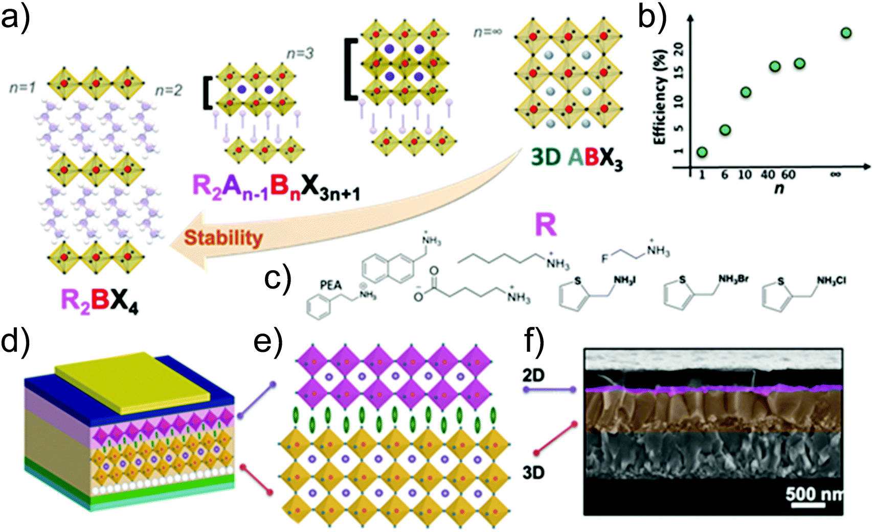 | ||
| Fig. 25 (a) Structure of perovskite from 2D to 3D forms. (b) η versus n. C) Typical cations used as R for the 2D perovskite formulation. (d) Structure of an n–i–p PSC based on FTO; cTiO2, mTiO2, 3D/2D perovskite, organic HTM, and Au CE. (e) Schematic of the 3D/2D active perovskite layer. (f) Cross-sectional SEM image of the 2D/3D device. | ||
The integration of 2D perovskites into PSCs as a stabilizer component has become increasingly popular in the last few years as a tool to increase the lifetimes of PSCs. Beyond that, a 2D perovskite also functions as a surface passivation layer, significantly improving the device VOC.1249,1250 In detail, the most common approach intends to combine the high efficiency of 3D perovskites with the superior stability of 2D perovskites by means of synergistic interface functionalization. This has been demonstrated by either mixing the 2D and 3D precursors together110,111 or by engineering a layer-by-layer deposition method to obtain a clean 2D/3D vertical bilayer architecture.966,1041,1042,1251,1252 The top 2D perovskite layers can simultaneously act as surface passivators, improving the surface robustness and hydrophobic character of the active layer, while also reducing surface charge recombination, ultimately improving the device open-circuit voltage.1040,1041,1059,1247,1253 Cho et al. developed a method for the deposition of a 3D/2D bilayer composed of mixed halide perovskites and (PEAI)2PbI4 (PEAI = phenethylammonium iodide).1251 The layer-by-layer growth is induced by the spin coating of PEAI in an isopropanol solution on the mixed halide 3D perovskite with PbI2 excess.1251 The PbI2 excess has been demonstrated to segregate on top of the 3D perovskite, reacting in situ with PEAI at the top surface and forming a thin 2D layer on top of the 3D material (the model of the device architecture is shown in Fig. 25d and e). Since the 2D perovskite lies on the top surface at the interface with the HTM, the interfacial charge carrier recombination is reduced, increasing η to values higher than 20%.1251 More recently, Jung et al. reported a double-layered halide architecture incorporating an ultrathin wide-bandgap halide stacked onto a narrow-bandgap halide light-absorbing layer. This layer effectively reduced charge recombinations at the perovskite/P3HT interface, resulting in an η value of around 23% and long-term operational stability.966 In addition to improving the surface robustness, imparting hydrophobicity, and passivating the surface, it has been recently demonstrated that the 2D overlayer is also crucial in preventing ion diffusion at the interface with the HTM.1040,1041 Sutanto et al. indeed observed a slower evolution (timescale of months) of the PV characteristics of 2D/3D PSCs using thiophene alkylammonium-based organic cations as the building blocks for the 2D perovskite (Fig. 25c).1040,1041 A boost in η has been associated with the slow structural rearrangement of the 2D/3D interface, which depends on the “softness” of the 2D perovskite overlayer that can act as an ion scavenger.1040 Because of the movement of ions in the 3D perovskite, small MA cations accumulate at the interface.1040 The 2D structure can incorporate the MA cations by altering its pristine layered structure into a mixed (or quasi-2D) phase.1040 In addition, a “more robust” 2D layer can prevent such structural changes, mechanically blocking the movement of ions.1040 This ion blockage leads to a dramatic increase in device stability, while maintaining high device η.1040 In addition, these 2D modifiers also dramatically improve the thermal stability of PSCs,1040 demonstrating that a conscious choice of proper 2D components can control the structural, physical, and energetic properties of the 2D/3D interfaces, a key element to be controlled for the design and realization of efficient and stable devices.11While defining the interface structure–function relationship is of utmost importance to control ion and charge accumulation and dynamical effects, the exact knowledge on interface energetics is also pivotal. To this end, it has been recently demonstrated that such thiophene-based cations form a p–n junction at the 2D/3D interface, which is the key to enable efficient charge transfer. As a consequence, electron accumulation at the interface is reduced, nullifying interfacial recombinations. This beneficial effect is reflected in the device VOC, which reached 1.19 V, among the highest reported so far in the literature.1254 As an illustrative example, an intact 2D/3D heterojunction, realized by growing a stable and highly crystalline 2D (C4H9NH3)2PbI4 film on top of a 3D perovskite (using a solvent-free solid-phase in-plane growth), reached a certified steady-state η of 24.35%, while retaining 94% of its initial η after 1056 h under the damp heat test (85 °C/85% relative humidity) and 98% after 1620 h under 1 sun illumination (without any encapsulation).1255 Meanwhile, substantial progresses have been recently achieved in controlling the film formation of 2D perovskites.1256 For example, an η value of 15.81% has been achieved using hot-cast Dion–Jacobson 2D perovskite ((PDMA)(MA)n−1PbnI3n+1 (PDMA = 1,4-phenylenedimethanammonium; 〈n〉 = 4)) as the photoactive layer.1255 Moreover, by elucidating the critical role of additives in regulating the nucleation and crystallization kinetics of 2D (PEA)2(MA)3Pb4I13 films with low trap states and desired carrier transport/collection properties, Yang et al. recently achieved an η value up to 18.5%, together with FF of 83.4%.1257
6.6 Tandem SCs based on PSCs
The tunability of the Eg value of perovskites via halide replacement1258 or cation exchange1259 and their high absorption coefficient across the entire visible range1260 make these materials attractive for tandem SCs, particularly in combination with Si sub-cells.In a Si/perovskite tandem configuration, higher-energy photons are absorbed by the perovskite sub-cell, while infrared photons are transmitted through the perovskite top cell and absorbed by the Si sub-cell, covering a wide absorption spectral range defined by the Eg value of Si.1261,1262
Therefore, the perovskite-based tandem configurations require the stacking of constituent sub-cells, with the perovskite top cell having two transparent electrodes, one of them directly processed on top of the charge selective layer (e.g., spiro-OMeTAD).1263,1264 Both high σ and optimal Tr of the top-cell transparent electrode are the key requirements for the successful design/realization of tandem devices. Conventional TCOs optically optimized for single-junction devices cannot be easily deposited onto the perovskite top cell due to the ion bombardment-induced degradation of the underlying materials during TCO sputtering.1265,1266 A strategy to minimize the underlying material damage is the deposition of additional buffer layers, which can absorb the energy impact of ions crashing on the device. Either thermally evaporated sub-stoichiometric molybdenum oxide (MoOx) buffer layers1267,1268 or ultrathin layers of Au1269 have been reported to protect spiro-OMeTAD during TCO sputtering. However, the aforementioned strategies inevitably add complexity to the perovskite top-cell fabrication process or cause additional optical losses. Moreover, the simplest solution offered by the MoOx buffer raises concerns on long-term stability, since the iodide of the perovskite layer can chemically react with MoOx, resulting in an unfavorable interface energy-level alignment for hole extraction.1270
In order to address these challenges, transparent graphene-based electrodes are promising for the realization of efficient and stable bifacial PSCs. Although graphene-based electrodes for PSC-based tandem SCs produced by solution-processed methods are still missing, several groups already reported their practical implementation through other techniques, such as CVD. For example, Lang and co-workers addressed this challenge by implementing large-area CVD-graphene as a highly transparent photoelectrode in a perovskite top-cell.1271 In fact, the electrodes based on graphene combined an excellent Tr (97.4%) with Rs of 100 Ω □−1.1272 Zhou and co-workers demonstrated two-layer CVD graphene as a transparent contact for a top cell based on a Cl-doped perovskite film with a bandgap of 1.59 eV.1273 The graphene electrodes permitted to achieve a top-cell η of 11.8%, resulting in a tandem SC with an η of 18.1%.1272
Even though solution-processed 2D material-based recombination layers or transparent conductive contacts have not been demonstrated in tandem devices yet, the use of graphene in the ETL of the perovskite top-cell was recently reported in a two-terminal (2T) mechanically stacked Si/perovskite tandem SCs.1274 With this approach, the sub-cells were fabricated and independently optimized and subsequently coupled by contacting the back electrode of the mesoscopic perovskite top-cell with the texturized and metallized front contact of the silicon bottom cell.1273 Then, the graphene-doped mesoporous ETL used in the perovskite top-cell allowed the tandem SCs to improve their η up to 26.3% over an active area of 1.43 cm2.1273 Overall, the “mechanical approach,” based on the independent optimization and fabrication of sub-cells, as well as graphene-based top cell, is ready to synergistically exploit the most recent progress achieved in both PSCs and Si cells in order to boost perovskite/silicon tandem SCs beyond current PV technology established in the market.1273
6.7 Summary and outlook
PSCs are an exciting PV technology aiming to enter a massive market. In fact, they can be produced through scalable and cost-effective solution-based techniques compatible with R2R and S2S manufacturing processes,1275 while reaching outstanding η up to certified values of 25.2%.897 This value approach to the record-high η of monocrystalline and HIT Si SCs (26.1 and 26.7%, respectively),897 even superior to those of thin-film PV technologies, such as CdTe and copper indium gallium selenide (CIGS) SCs (22.1% and 23.4%, respectively).897 Furthermore, perovskite-based tandem SCs, namely, perovskite-Si tandem SCs, have reached certified η up to 29.1%,897 which is as high as the value of costly GaAs SCs (that holds the record-high certified η for single-junction cells).897 Prospectively, the LCOE of perovskite solar panels has been estimated to be lower than 5 US cents kW h−1.131–133 This value is competitive with the LCOEs of fossil fuels,134,135 thus enabling the achievement of grid parity. However, the instability of photoactive perovskites1001,1276–1278 and CTLs1001,1277 represents the main technical barrier for PSC technology. In this scenario, the use of solution-processed 2D materials in PSCs demonstrated exciting results in resolving current PSC issues, boosting both stability and η by means of scalable and cost-effective strategies.1037,1279,1280 These advances can be ascribed to the progresses achieved in the preparation of 2D material inks and their large-area (i.e., wafer-scale) printing,205,297,1281,1282 addressing controllable optoelectronic properties to be exploited in PSC structures.1192 By formulating 2D material-based inks in solvents compatible with materials composing the PSCs, GRMs have been successfully integrated as both CTLs and interlayers,1283 improving the charge collection (while providing effective barriers against humidity) and migration of ions within the PSC structures.1037,1284,1285 Graphene and its derivatives have also been investigated to form efficient back electrodes (CE) as an alternative to Au or Ag.1217,1227 Beside reaching relevant η up to 18.65%,1230 the use of metal-free back electrodes eliminates the degrading reaction between the perovskite layer and Au and Ag, which are the cause of device instability.1219,1286,1287 Recent advances in low-temperature processable graphene inks are promising for the realization of paintable C-PSCs based on structures that achieved record-high η using metal-based back electrodes.1217 Importantly, graphene and other GRMs (e.g., MoS2) can also regulate the perovskite crystal over both mesoscopic scaffolds and planar CTLs,1104,1160 increasing the reproducibility of high-η devices. Besides, pristine FLG flakes were used to stabilize perovskite films, slowing down charge thermalization.1106 The realization of 2D material-enabled hot-carrier extraction and collection paves the way for the creation of advanced SC concepts, which are still unexplored.1106Despite the implementation of GRMs has not been reported yet for PSCs showing state-of-the-art η, outstanding results have been achieved in large-area PSCs and PSMs.1192 The deposition of 2D material-based inks by means of printing techniques, such as slot-dye coating, blade coating, spray coating, and screen printing have been established in a wide range of applications, including energy storage and conversion systems beyond SCs.5,207,1288 For the case of PSCs, the printing processes of 2D materials can be easily customized and optimized in combination with a protective layer on top of the perovskite absorber, such as 2D perovskite1289 or polymeric interlayer (e.g., PMMA).1290 As a striking example of PSC scale-up, some authors of the present review (belonging to University of Rome Tor Vergata, Hellenic Mediterranean University, Italian Institute of Technology, and BeDimensional S.p.A.), in collaboration with the industrial partner GreatCell Solar, realized the first example of real-time characterized, standalone 2D-material-enabled perovskite solar farm. The latter was installed in 2020 in Heraklion (Crete), a site with favorable climate conditions. Initially, it comprised 9 solar panels, each one with an active area of 0.32 m2 (Fig. 26). According to the planned activity, other panels will be integrated into the solar farm, and the output of the solar farm will be continuously monitored, providing a clear understanding of (1) the correlation of environmental conditions with the outdoor performance of solar panels and (2) the benchmarking of 2D material-based perovskite solar panels against conventional PV technologies (Si, CdTe, and CIGS). The preliminary data, provided to the Commission of the European Union (project founders),1291 revealed the key advantages of 2D materials in providing PV FoMs competitive in the market, bringing PSC commercialization closer to reality. It is noteworthy that under the umbrella of European Graphene Flagship, the solar farm project has been recently extended to a graphene-integrated perovskite–silicon tandem SC technology, involving a key player of the PV industry, namely, Enel Green Power and Siemens.1292,1293 Not by chance, the results achieved using 2D materials on single-junction PSCs have already been exploited in perovskite-based tandem SCs, namely, a perovskite–Si tandem device.1273 In particular, the doping of TiO2-based ETLs of PSCs with graphene flakes enabled the tandem devices to reach η over 26%.1273 Nevertheless, the incorporation of GRMs in perovskite-based tandem devices is still at a premature stage. Prospectively, solution-processed graphene and other metallic 2D materials can play a major role in developing advanced interconnecting layers with a satisfactory trade-off between optical transparency and electrical conductivity.
 | ||
| Fig. 26 2D materials-enabled perovskite solar farm installed in Heraklion (Crete). | ||
Lastly, it is worth noting that 2D materials can play a relevant role in developing new encapsulation strategy for perovskite devices, which are particularly sensitive to oxygen, moisture, and volatilization of internal species (i.e., decomposition products and dopants).1294,1295 For example, a recent work demonstrated a cost-effective and scalable flexible transparent lamination encapsulation method based on graphene films with a PDMS buffer on a PET substrate.1296 Moreover, the impermeability of graphene or other related materials can be successfully exploited to create novel encapsulants or edge sealers, decreasing the water vapor transmission rate (WVTR) or oxygen transmission rate (OTR) of the current encapsulants used in PSCs, as well as other PV technologies.
Overall, 2D materials are expected to play protagonists in the optimization of perovskite-based PV technology, which could represent a game changer in the PV market for the near future.
7. Other SCs
7.1 QDSCs
QDSCs are an attractive PV technology owing to various advantages,1297 such as cost-effectiveness and simple device manufacturing processes.57,1298–1307 As comprehensively discussed in recent review articles (for example, ref. 1296), such SCs are based on photoactive semiconductors (organic, inorganic, or hybrid) QD films, which act as both absorbers and charge transporting media. Different types of QDSC architectures have been proposed: (1) Schottky QDSCs, which consist of a heterojunction between a planar film of p-type colloidal QDs and a shallow-Φw metal, which produce a Schottky barrier generating a depletion region for carrier separation;1308–1313 (2) depleted heterojunction QDSCs, which use a highly doped n-type metal oxide (typically, TiO2 or ZnO, but even metal chalcogenides, e.g., CdS) in a p–n heterojunction with a p-type QD film;1314–1316 (3) heterojunction QDSCs, also referred to as QD-sensitized solar cells (QDSSCs), in which the n-type wideband-gap semiconductor and QD film form an interpenetrating layer.1296,1301,1317–1325 This structure is usually obtained by infiltrating QDs into the structured n-type semiconductors. Since this architecture resembles that of DSSCs, such cells are often referred to as QD-based DSSCs (QDDSSCs) (see Section 5); (4) quantum junction QDSCs, which consist of a homojunction-like architecture where both p- and n-type materials of the junction are composed of QDs;1326 (5) bulk nanoheterojunction SCs in which an n-type material and p-type QDs are mixed similar to a BHJ architecture.1327The optoelectronic properties of semiconductor QDs, e.g., Eg, optical absorption coefficient (α), and charge carrier transport, can be effectively tuned by modulating their size and shape,1298–1304,1328 offering versatile systems to be used in graded doping architectures1329–1331 and multijunction (tandem) SCs.1332,1333 Initially, chalcogenide semiconductors, such as CdX and PbX (X = S, Se, and Te), have been used for QDSCs due to their ability to harvest light in the visible and IR regions and their low cost.1300,1304–1306,1327,1334 However, the limited η achieved with these inorganic QDs drove researchers to design novel QDs, including inorganic alloys, organic, and organic–inorganic hybrid QDs with superior PV capabilities.1304–1306,1327 Therefore, over the past decade, QDSCs have seen rapid improvements, until reaching a certified η value of 16.6% with mixed Cs and formamidinium lead triiodide perovskite system1335 (previous record was 13.4%).1336 These important results are the fruits of progress achieved in both control of the QD surface chemistry and the understanding of device physics,1305,1306,1337 and they are now leading QDSCs toward commercialization.1305,1306
Despite recent progresses, the record-high η of the QDSCs is still far from their theoretical maximum η, which is as high as 33%1338 (or 44%, depending on whether or not multiple exciton generation of the QDs is considered).1337,1339 Actually, the major issue in QDSCs is the presence of structural defects or unpassivated states on the QD surface, which leads to recombination reactions limiting the overall performance of the devices.1340–1347 To resolve this issue, several strategies, including the implementation of atomic ligand/anionic passivation schemes,1348–1350 use of passivation layers over QD films,1351–1355 and design of core–shell structures,1356–1363 have been developed in various type of QDSCs. For example, a hybrid passivation scheme, which introduces halide anions during the end stages of the QD synthesis process, was used to realize depleted heterojunction QDSCs with a certified η value of 7.0%.1347 Sequential inorganic ZnS/SiO2 double-layer treatment onto the QD-sensitized photoanode strongly inhibited the interfacial recombination processes in QDSSCs, which reached a certified η value of 8.21%.1354 CdSeTe/CdS type-I core–shell QDSSCs, obtained by overcoating CdS shells around CdSeTe-core QDs, achieved an η value of 9.48%.1357 Binary QD films have also been investigated in heterojunction QDSCs in order to improve the charge separation using p–n junctions at the nanoscale, while passivating possible surface defects of QDs.1326,1364,1365 In addition, such junctions enabled the dissociation of excitons in free carriers, drastically reducing bimolecular recombination processes.1326,1363,1364 The use of mixed QD films was targeted to extend the carrier diffusion length, allowing thicknesses of the photoactive films to become comparable to the optical absorption length.1363,1364 However, binary QD systems have limitations in simultaneously controlling the Eg value as well as CB and VB edges for both charge photogeneration and collection. Hence, to overcome the limitations of binary QDs, alloy QDs1366,1367 and hybrid organic–inorganic QDs1334,1368,1369 have been successfully proposed together with the abovementioned strategy to passivate surface defects. For example, Du et al. reported a Zn–Cu–In–Se-alloyed QD sensitizer to construct Pb- and Cd-free QDSSCs with a certified η value of 11.61%.1370 Very recently, the Cs1−xFAxPbI3 system in the form of QDs enabled the realization of QDSSCs with a certified record η of 16.6%, together with superior stability (94% of the original η under continuous 1 sun illumination for 600h) compared with their thin-film counterpart.1334
In addition to the aforementioned strategies, the engineering of various QDSC configurations through the introduction of interfacial layers and doping of components is crucial to improve the charge extraction and transport from the photoactive layer to the metal contacts, thereby achieving performance rivaling those of other PV technologies. Especially in this context, solution-processed graphene and other 2D materials have attracted a primary interest for QDSCs. Tavakoli et al. reported an in situ solution-based process to prepare hybrid ZnO/graphene QDs (Fig. 27a and b), where the graphene shell quenches the PL intensity of ZnO nanocrystals (size of NPs: 5 nm) by ∼72%, primarily due to charge transfer and static quenching.1371 This nanocomposite was used as a CE material in a PbS/TiO2 depleted heterojunction QDSCs, which achieved an η value of up to 4.5%.1370Fig. 27c shows a schematic of the architecture of the device, in which fast electron extraction is achieved by means of ZnO–graphene CE (Fig. 27d).1370 In particular, the band diagram of device shows the electron extraction process from PbS to ZnO–graphene-coated TiO2 (Fig. 27e).1370
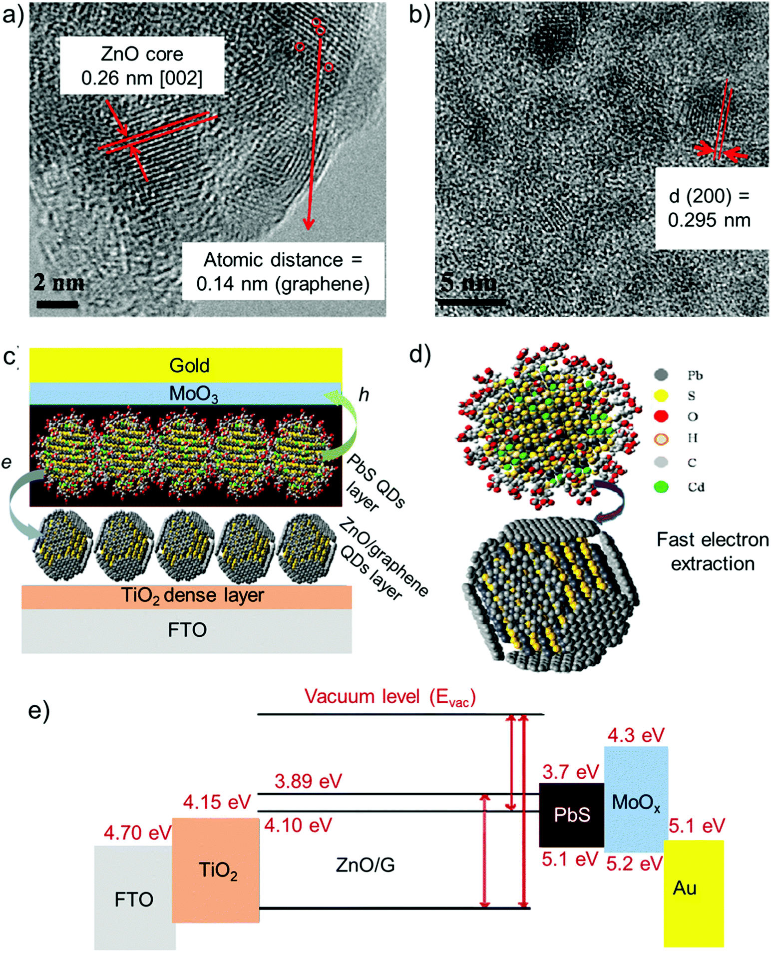 | ||
| Fig. 27 High-resolution TEM images of (a) graphene QDs and (b) ZnO/graphene QDs. (c) PbS QD and ZnO/graphene QD-based depleted heterojunction QDSCs. (d) Schematic of the electron extraction process from PbS QD to ZnO/graphene QD. (e) Energy-level diagram of PbS QD- and ZnO/graphene QD-based depleted heterojunction QDSCs (G = graphene). Adapted from ref. 1370. | ||
The authors explained their results by suggesting efficient electron injection from the CB of ZnO QDs to the LUMO levels of graphene, which occurs through Zn–O–C bonding, and slow electron recombination in the presence of ZnO-graphene buffer layer.1370 Graphene frameworks were incorporated into the TiO2 photoanode as an electron transport medium to improve the PV performance of QDSSCs (up to an η value of 4.2%) owing to their excellent conductivity and isotropic framework structure.1372
Kim et al. reported the use of a hierarchical ZnO nanostructure array, produced by a two-step solution reaction and composed of nanosheet branched ZnO nanorods as an efficient anode for QDSSCs.1373 This 2D (nanosheet)–1D (nanorod) combined hierarchical ZnO nanostructure considerably enhanced light capture compared with ZnO thin films and ZnO nanorods, allowing the corresponding CdSe/CdS-based QDSSCs to achieve an η value of 4.4%.1372
Recently, 2D MoS2 nanosheets were used as an efficient HTL for PbS-based depleted heterojunction QDSCs.1374 All-solution-processed n–p–p+ architecture was fabricated by sequentially depositing ZnO NPs, PbS QDs, and 2D MoS2 nanosheets acting as n-, p-, and p+-type layers, respectively.1373 The incorporation of MoS2 HTL improved the η value from 0.92% (in the free-MoS2 reference) to 2.48%.1373
Noteworthily, 2D MoS2 has recently been coupled to Sn-doped In2O3 nanocrystals to collect holes from the latter and driving permanent charge separation across a novel type of ultrathin solid-state 0D/2D hybrid interface that can store light in the contactless mode.1375 Therefore, these results further prove the potential of MoS2 as the HTL in QD-based optical devices.
Jin et al. reported graphdiyne, which is a π-conjugated structure consisting of sp2- and sp-hybridized carbons in a typical 2D configuration, as a potential solution-processed hole transporter for PbS-based QDSCs, which reached an η value of 10.64%.1376 The use of graphdiyne-based anode buffer layer improved hole extraction from the QDs to Au anodes, while providing long-term shelf-life stability over 120 days.1375
Dangling bond-free 2D h-BN with self-terminated atomic planes, produced through LPE in 2-propanol, was used to passivate the TiO2 surface in CdSe-based QDSCs.1377 By decreasing the recombination rate at the TiO2/CdSe interface, the resulting QDSCs achieved an η value of 7%, corresponding to a 46% improvement in η exhibited by the h-BN-free reference.1376
In addition to the aforementioned roles of 2D materials in QDSCs, liquid-phase synthetized antimonene QDs have been applied as the photoactive layer in QDSSCs.1378 Owing to their strong light–matter interaction, moderate Eg for an optimal absorption in the visible spectrum, and antioxidation properties, antimonene QDs enabled the realization of QDSSCs with an η value up to 3.07%.1377 Moreover, the as-fabricated SCs have shown long-term stability, retaining more than 90% of the initial η after 1000 h.1377 Therefore, antimonene QDs, as well as other 2D material-derived QDs, may provide a new pathway for a novel kind of cost-effective solution-processed QDSCs.1377
Although the above examples clearly indicate that 2D materials can play a significant role in further improving the performance of QDSCs, their use in this type of SCs is not strongly established as those for OSCs, DSSCs, and PSCs. However, both the advent of a novel type of efficient QDSCs and successful implementation of 2D materials in other PV devices can provide the fundamentals for the future establishment of 2D material-enabled efficient QDSCs.
7.2 Organic–inorganic hybrid SCs
Organic–inorganic hybrid SCs combine organic and inorganic materials as the photoactive material. As discussed in previous reviews in the literature,1379–1385 the rationale of this combination is to implement the advantages offered by both OSCs and inorganic components. As proposed for OSCs (Section 3), organic materials are solution-processable and thus compatible with low-cost and high-throughput deposition methods, including R2R printing techniques. Moreover, they have high σ in the visible spectrum. Thus, they allow their thin (thickness of a few hundred nanometers) films to efficiently absorb solar light. Meanwhile, inorganic materials can be formulated in the form of solution-processable nanocrystals with tunable optoelectronic properties, as shown in Section 7.1 for QDSCs. Furthermore, they have a large dielectric constant (e.g., ∼10.4 for CdSe),1386 which decreases the Coulombic attraction between electrons and holes, facilitating their separation in free charges. Thus, when mixed with organic photoactive components, they can provide an interfacial force driving the dissociation of excitons generated in the organic materials in free charge.1387–1390 Therefore, inorganic nanocrystals can act as ideal acceptor materials in BHJ OSC-like devices using either organic polymers or conjugated small molecules as the donors.1378–1384,1391The first hybrid SC was reported in 1996 using CdSe nanodots as the acceptor and poly[2-methoxy-5-(2′-ethylhexyloxy)-p-phenylene vinylene] (MEH-PPV) as the donor.1392 However, the corresponding η was low (<0.5%) as a consequence of the poor charge transport through the CdSe nanodots.1391 Thereafter, much effort has been devoted toward improving charge transport by tuning the nanocrystal shapes.1393–1395 Studies on QDSCs also helped to rapidly advance hybrid SCs.1396 In 2011, Ren et al. reached an η value of 4.1% with hybrid SCs based on P3HT and CdS nanocrystals as the donor and acceptor, respectively.1397 More recently, hybrid SCs based on Si as the inorganic component have drawn relevant attention due to their room-temperature, facile, and cost-effective fabrication processes, which is promising to lower the cost of conventional Si SCs.1398–1400 Owing to advances in the synthesis of organic materials and design of novel device structures, hybrid SCs based on n-type Si substrate achieved η higher than 16%,1401,1402 (record value of 17.4%).1403 Despite the aforementioned results, the η value of hybrid SCs is still insufficient to compete with conventional inorganic Si SCs and PSCs (Section 6). Moreover, the stability of hybrid SCs is also limited compared to conventional inorganic PV technology.1404–1407 These drawbacks are strongly hindering the commercialization of hybrid SCs at a large scale. In this context, the incorporation of GRMs can help resolve both η and stability limits of hybrid SCs. For example, RGO has been proposed to produce a buffer layer in hybrid SCs to improve the light-induced charge extraction of ∼50%, as well as to replace the PEDOT:PSS contact.1408 Recently, GQDs were mixed with PEDOT to be used in hybrid SCs using PEDOT:GQDs/porous Si/n-Si/TiOx structure.1409 In detail, GQDs improved the conductivity of PEDOT, porous Si reduced the overall reflectivity, and TiOx acted as a passivation layer to reduce the recombination layer.1408 The as-produced devices reached a maximum η value of 10.49%, retaining 78% of the initial η under ambient conditions for 15 days.1408 GQDs, produced through a top-down strategy based on laser fragmentation in a post-hydrothermal treatment, were also used as a buffer layer between TiO2 and P3HT to form a cascade energy-level scheme in hybrid SCs.1410 The introduction of GQDs into a BHJ hybrid SC led to the enhancement of η from 2.04% to 3.16%.1409
Although the aforementioned examples demonstrated the potential of GRMs in hybrid SCs, further studies are needed to formulate 2D materials in overcoming the fundamental issues exhibited by such type of SCs. Both progresses of 2D material science and hybrid SC-related technology could help for an in-depth reconsideration of 2D material-enabled hybrid SCs.
8. Outlook and conclusions
Several progresses have been achieved in the use of graphene and related 2D materials (GRMs) in solution-processed PVs. Regarding TCE applications, the implementation of solution-processed 2D materials is still at a premature stage. In fact, solution-processed graphene-based films typically exhibit sheet resistance (Rs) values in the order of kΩ sq−1 (for Tr ≥ 80%),1411 which are significantly higher than typical benchmarks (e.g., less than kΩ sq−1 for ITO and FTO films). The origin of such low performance is mainly ascribed to the low lateral size of the liquid-phase exfoliated graphene flakes (typically in the order of few micrometers for high-quality graphene flakes)359 and the high contact resistance between the graphene flakes composing the electrode. However, the development of hybrids between solution-processed graphene and metal nanowires or CNTs, as well as the use of micromesh structures on top of the graphene-based films, represent promising approaches to overcome the current limitations. Prospectively, they could allow the design/realization of TCEs compatible with R2R large-area manufacturing. However, the high cost of metal nanowires1412 (several hundreds of dollars per kilogram),1413 CNTs (even more than 1000 $ kg−1 for single-walled CNTs)1414 and microscale metal grids ($30–40 m−2)1411 is not lower than the cost of ITO ($5 m−2 for a film with Rs of 150 Ω sq−1 films and higher than $20 m−2 for films with Rs of 10 Ω sq−1,1415 or 600 $ kg−1),1416 making currently available graphene-based TCEs not competitive for massive use in large-area PV devices. Recently, transparent electrodes have also been demonstrated by spin coating 2D Ti3C2 from an aqueous dispersion for photodetector applications.1417 However, as for the case of solution-processed graphene, such a transparent electrode shows high sheet resistance, still being ineffective in collecting current density in the order of tens of milliamperes, as those displayed by PV devices. In addition, it should be noted that 2D materials have been used to develop efficient, transparent CEs for bifacial DSSCs, which emerged as interesting systems for both BIPVs and tandem SCs.878–880,889The most successful applications of GRMs in PV technologies rely on their use in the form of CTLs for both holes and electrons (or interlayers in tandem PV architectures). For example, GRMs effectively act as dopants to improve the properties of traditional CTLs. The amount of GRMs needed for this purpose is often minimal, in the order of few weight (volume) percentages of the overall material (dispersion). For example, just 1.6 mL of graphene flakes dispersion at a concentration of 1 g L−1 is sufficient to realize 1 m2 of advanced ETLs for PSCs.1107,1192,1273 By considering η higher than 18% in single-junction SCs,1107,1192 and even higher than 25% in tandem SCs,1273 only a few grams of graphene flakes are needed for the realization of a 1 MWp PV plant. This amount of graphene flakes corresponds to a negligible added marginal cost, in the order of tens of dollars per megawatts-peak.205,328,359 Thus, the integration of graphene and other metallic 2D materials,1418 including group-5 TMDs (e.g., TaS2, TaSe2, NbS2, NbS2, VS2, VSe2, etc.), group-6 TMDs (e.g., the 1T polytype of MoS2 and WS2), topological insulators (e.g., Bi2S3, Bi2Se3, and Bi2Te3), and MXenes, as dopants in the CTL is an approach that can be immediately implemented on different solution-processed PV technologies at the industrial scale, without increasing the overall costs. Beyond their use as dopants, GRMs have been successfully used for the realization of a thin buffer layer (or interlayer) to improve the extraction/collection of the charge photogenerated in the photoactive layer of the cells toward the CTLs and current collectors. In this context, several studies have focused on the formulation of 2D material dispersions in solvents compatible with other materials composing the SC structure. For example, 2D TMD inks have been formulated in 2-propanol to be deposited as a buffer layer over the perovskite layer for the realization of PSCs, showing η exceeding 20%. Therefore, the incorporation of 2D material-based buffer layers into the most advanced SC architectures is highly promising to further boost the η value of PV technologies beyond the current record-high values. In addition, 2D material-based buffer layers can have a tangible impact on the enhancement of the long-term stability of SCs, particularly for OSCs and PSCs. In fact, 2D materials intrinsically act as shielding layers against humidity, offering promising potential as oxygen/moisture barriers. Moreover, they can also provide effective barriers against ion migration, stabilizing the photoactive perovskite layers or blocking metal/ion migration effects, which determines the degradation of PV devices. With regard to dopants, the amount of 2D materials required for the realization of thin films of 2D materials can be minimal, allowing almost zero additional costs. Not by chance, TMD-based buffer layers (e.g., MoS2) have been used by research groups comprising authors of this work to build a 2D material-enabled solar farm (Fig. 26), without any significant impact over the technology lifecycle assessment (LCA) (data unpublished but reviewed by the European Commission in the context of the Graphene Flagship project).1290
Another prospective application of 2D materials in solution-processed SCs is their use as additives in photoactive layers. In particular, the use of GRMs as energy cascade materials can increase the solar-light absorption, whilst eliminating charge recombination pathways occurring in the native materials. In addition, 2D materials can alter the interfacial properties of the photoactive material in contact with other materials composing the SC structure. Such effects can be used to improve charge transfer toward the CTLs (or current collectors), as recently shown with MXenes.1125 Therefore, the implementation of 2D material-based buffer layers has higher potential for boosting the PV performance of 3rd-generation SCs toward commercially competitive values. To accomplish these, the chemical functionalization of GRMs can be a key step to tune on-demand their optoelectronic properties, thereby adequately matching their energy levels with those of the active materials and CTLs. In addition to GRMs, 2D perovskites have been recently established to improve the thermal stability of PSCs,1040 demonstrating that rational perovskite engineering can advantageously regulate the structural, physical, and energetic properties of 2D/3D interfaces for the realization of efficient and stable PSCs.111 Thus, the impact of 2D materials on the structural and optoelectronic properties of the photoactive layer represents a current “hot topic” for the future optimization of current state-of-the-art SCs. Even though the success of solution-processed 2D materials has been established in several PV technologies, we notice that major efforts are currently focused on PSCs, probably because of their attracting η exceeding 25%, together with their advantageous combination with Si SCs in tandem systems. In this context, the use of solution-processed 2D materials combined with advanced strategies proposed for optimizing the photoactive layer formulation and processing, as well as for device structure engineering, is promising to boost the η of SCs beyond the current state-of-the-art values. The same approach is also viable in enabling similar performance over large-area systems (from a module up to a solar farm). Moreover, the outcomes consolidated for PV technologies discussed in this work could also be extended to other types of thin-film SCs and Si SCs, in which the implementation of solution-processed 2D materials is still premature. Overall, we do believe that the conscious use of the ever-growing 2D materials portfolio can renew the expectation for the rapid establishment of advanced PV technologies worldwide. To accomplish these advances, the standardization of the morphological and structural characterization of 2D materials is crucial for the establishment of industrial-scale technologies, which also requires the setting up of reliable 2D material suppliers with a massive production capability. In this context, the recent standardization sequence of methods for characterizing the structural properties of graphene, bilayer graphene, and graphene nanoplatelets (SO/TS 21356-1:2021) represents a step forward toward the upscaling of solution-processed 2D material-enabled SCs. Meanwhile, emerging solution-processed 2D materials, such as nonlayered materials, carbon nitrides (CxNy), 2D c-MOFs, layered double hydroxides, and other poorly investigated GRMs (e.g., metal monochalcogenides, group-4 and group-5 TMDs, and polar and/or ferroelectric non-centrosymmetric materials) represent a playground for the realization of cutting-edge concepts of SCs.
Abbreviations
| 2D c-MOF | Two-dimensional conjugated metal–organic framework |
| AFM | Atomic force microscopy |
| AgNWs | Silver nanowires |
| ALD | Atomic layer deposition |
| ANIGQDs | Aniline graphene quantum dots |
| APjet | Atmospheric plasma jet |
| a-Si | Amorphous silicon |
| α | Optical absorption coefficient |
| α vis | Optical absorption coefficient in the visible spectrum |
| BCP | Bathocuproine |
| BHJ | Bulk heterojunction |
| BIPVs | Building-integrated photovoltaics |
| BP | Black phosphorus |
| BPNFs | Black phosphorus nanoflakes |
| BPQDs | Black phosphorous quantum dots |
| CCG | Chemically converted graphene |
| CB | Conduction band |
| CE | Counter electrode |
| CIGS | Copper indium gallium diselenide |
| CIGSSe | Copper indium gallium selenide sulfide |
| C-PSC | Carbon perovskite solar cell |
| CQDs | Carbon quantum dots |
| CZTSe | Copper zinc tin sulfur-selenide alloy |
| CNTs | Carbon nanotubes |
| c-Si | Crystalline silicon |
| CTAB | Cetyl-trimethyl-ammonium-bromide |
| CV | Cyclic voltammetry |
| CVD | Chemical vapor deposition |
| D n | Electron diffusion coefficient |
| DGU | Density gradient ultracentrifugation |
| DSSC | Dye-sensitized solar cell |
| δ p | Optical penetration depth |
| ECS | Energy conversion and storage |
| EDNB | Ethylenediamine dinitrobenzoyl |
| e | Elementary charge |
| e− | Electron |
| E F | Fermi energy level |
| E g | Optical bandgap |
| E ph | Photon energy |
| EIS | Electrochemical impedance spectroscopy |
| EpD | Electrophoretic deposition |
| EQE | External quantum efficiency |
| ETLs | Electron transporting layers |
| e-graphene | Electrochemically exfoliated graphene |
| FA | HC(NH2)2 |
| FF | Fill factor |
| FGSs | Functionalized graphene sheets |
| fMoS2 | Functionalized molybdenum disulfide |
| FoM | Figures of merit |
| FRGO | Fluorinated reduced graphene oxide |
| FTO | Fluorine-doped tin oxide |
| ϕ W | Work function |
| GMo | Graphene-molybdenum disulfide heterostructure |
| GNPs | Graphene nanoplatelets |
| GNSs | Graphene nanosheets |
| GNRs | Graphene nanoribbons |
| GO | Graphene oxide |
| GO-EDNB | Graphene oxide functionalized with ethylenediamine's amino groups |
| GO-TPP | Graphene oxide linked with porphyrin moieties |
| GO-Cl | Chlorinated graphene oxide |
| GQDs | Graphene quantum dots |
| GRMs | Graphene-related materials |
| GSs | Graphene sheets |
| h-BN | Hexagonal boron nitride |
| HIT | Heterojunction with intrinsic thin layer |
| HOMO | Highest occupied molecular orbital |
| HTLs | Hole transporting layers |
| HSN | Hierarchically structured nanoparticles |
| η | Solar-to-electrical energy conversion efficiency |
| h+ | Hole |
| h | Planck's constant |
| ħ | Reduced Planck's constant |
| I | Electrical current |
| ICBA | Indene–C60 bisadduct |
| ICLs | Interconnection layers |
| IGO | Imidazole-functionalized GO |
| I MPP | Current at the maximum power point |
| I SC | Short-circuit current |
| IQE | Internal quantum efficiency |
| ITO | Indium–tin oxide |
| k B | Boltzmann's constant |
| κ | Molar extinction coefficient |
| LCOE | Levelized cost of energy |
| Li-TFSI | Lithium bis(trifluoromethanesulfonyl)imide |
| LPE | Liquid phase exfoliation |
| LRGO | Laser-treated reduced graphene oxide |
| LUMO | Lowest unoccupied molecular orbital |
| λ | Photon wavelength |
| MA | CH3NH3 |
| MBE | Molecular beam epitaxy |
| MEH-PPV | Poly[2-methoxy-5-(2′-ethylhexyloxy)-p-phenylene vinylene] |
| MGO | Multilayer graphene oxide |
| MIR | Mid-infrared |
| MLG | Multilayer graphene |
| MOF | Metal–organic framework |
| MPA | 3-Mercaptopropionic acid |
| MPPT | Maximum power point |
| mTiO2 | Mesoporous TiO2 |
| MWCNTs | Multiwalled carbon nanotubes |
| μ | Charge carrier mobility |
| μ e | Electron mobility |
| μ h | Hole mobility |
| N d | Charge carrier density |
| n film | Film refractive index |
| n sub | Substrate refractive index |
| η th | Theoretical solar-to-electrical energy conversion efficiency |
| NFA | Non-fullerene acceptors |
| NG/NiO | N-Doped graphene@nickel oxide |
| N-GFs | N-Doped graphene frameworks |
| NGNP | N-Doped graphene nanoplatelets |
| NP | Nanoparticles |
| NG | Amino-functionalized graphene |
| NIR | Near-infrared |
| NR | Nanorods |
| NRGO | Nitrogen-doped reduced graphene oxide |
| OLED | Organic light-emitting diodes |
| O-MoS2 | Oxygen-incorporated molybdenum disulfide |
| OSCs | Organic solar cells |
| OTR | Oxygen transmission rate |
| oxo-G | Organo-sulfonate graphene |
| PEAI | Phenethylammonium iodide |
| (PEA)2PbI4 | Phenyl ethyl ammonium lead iodide |
| P in | Power of incident light |
| PC61BM | [6,6]-Phenyl-C61-butyric acid methyl ester |
| PC71BM | [6,6]-Phenyl-C71-butyric acid methyl ester |
| PCDTBT | PC71BM:poly[N-9′-heptadecanyl-2,7-carbazole-alt-5,5-(4′,7′-di-2-thienyl-2′,1′,3′benzothiadiazole)]):[6,6]-phenyl-C71-butyric acid methyl ester |
| PDINO | N,N-Dimethyl-ammonium N-oxide)propyl perylene diimide |
| PDINO-G | Graphene doped with N,N-dimethyl-ammonium N-oxide)propyl perylene diimide |
| PDMS | Polydimethylsiloxane |
| PEDOT:PSS | Poly(3,4-ethylenedioxythiophene) polystyrene sulfonate |
| PET | Poly(ethylene terephthalate) |
| PFN | Poly((9,9-bis(3′-(N,N-dimethylamino)propyl)-2,7-fluorene)-alt-2,7-(9,9-dioctylfluorene)) |
| PFN-Br | Poly9,9-bis6-(N,N,N-trimethylammonium)hexylfluorene-alt-co-phenylenebromide |
| P3HT | Poly(3-hexylthiophene) |
| P3HT:PC61BM | Poly(3-hexylthiophene):[6,6]-phenyl C61-butyric acid methyl ester |
| P3OT | Poly(3-octylthiophene-2,5-diyl |
| PH1000 | Poly(3,4-ethylenedioxythiophene):poly-(styrenesulfonate) |
| PMMA | Polymethyl methacrylate |
| PM6 | Poly[[4,8-bis[5-(2-ethylhexyl)-4-fluoro-2-thienyl]benzo[1,2-b:4,5-b′]dithiophene-2,6-diyl]-2,5-thiophenediyl[5,7-bis(2-ethylhexyl)-4,8-dioxo-4H,8H-benzo[1,2-c:4,5-c′]dithiophene-1,3-diyl]-2,5-thiophenediyl] |
| PTB7:PCB71M | Thieno[3,4-b]thiophene/benzodithiophene:phenyl-C71-butyric acid methyl ester |
| PTAA | Poly(triaryl)amine |
| pRGO | Partially reduced graphene oxide |
| PSCs | Perovskite solar cells |
| PSMs | Perovskite solar modules |
| PV | Photovoltaic |
| QDs | Quantum dots |
| QDDSSCs | Quantum dot-based dye sensitized solar cells |
| QDSCs | Quantum dot solar cells |
| QDSSCs | Quantum dot-sensitized solar cells |
| R2R | Roll-to-roll |
| R CT | Charge transfer resistance |
| R S | Sheet resistance |
| R TiO2 | Transport resistance of electrons in the TiO2 film |
| R TCO–TiO2 | Resistance at transparent conductive oxide/TiO2 contact |
| R rec | Charge transfer resistance of the charge recombination between electrons in the TiO2 film and I3− in the electrolyte |
| R CT | Charge transfer resistance at the counter electrode/electrolyte interface |
| R TCO–electr. | Charge transfer resistance at the TCO/electrolyte interface |
| RGO | Reduced graphene oxide |
| RGOMM | Reduced graphene oxide micromesh |
| rGS | Reduced graphene scaffold |
| RH | High humidity environment |
| RT | Room temperature |
| S–Q | Shockley–Queisser |
| SBS | Sedimentation-based separation |
| SCs | Solar cells |
| SLG | Single-layer graphene |
| Spiro-OMeTAD | 2,2′,7,7′-Tetrakis[N,N-di(4-methoxyphenyl)amino]-9,9′-spirobifluorene |
| SSA | Specific surface area |
| SWCNT | Single-walled carbon nanotube |
| σ | Electrical conductivity |
| σ dc | d.c. conductivity |
| σ opt | Optical conductivity |
| t | Photoactive material thickness |
| TBP | Tert-butylpyridine |
| TCEs | Transparent conductive electrodes |
| TCOs | Transparent conductive oxides |
| TCPP | Tetrakis(4-carboxyphenyl)porphyrin |
| TEGr | Thermally exfoliated graphene |
| TEM | Transmission electron microscopy |
| TFSCs | Thin-film solar cells |
| TFSI | Trifluoromethanesulfonyl imide |
| TMD | Transition metal dichalcogenide |
| ToF-SIMS | Time-of-flight secondary ion mass spectrometry |
| T r | Optical transmittance |
| TRGO | Thermally reduced GO |
| TSHBC | Perthiolated tri-sulfur-annulated hexa-peri-hexabenzocoronene |
| τ | Electron lifetime |
| UVO | UV-ozone |
| VB | Valence band |
| V MPP | Voltage at the maximum power point |
| V OC | Open-circuit voltage |
| WVTR | Water vapor transmission rate |
| WJM | Wet-jet milling |
| XPS | X-ray photoelectron spectroscopy |
| XRD | X-ray diffraction |
| Z | Vacuum impedance |
| Z d | Warburg impedance |
| ZnP | Zn–porphyrin |
| ZSO | Zinc stannate |
Conflicts of interest
There are no conflicts to declare.Acknowledgements
This project has received funding from the European Union's Horizon 2020 research and innovation program under grant agreements No. 785219 and 881603-GrapheneCore2 and GrapheneCore3, the MSCA-ITN ULTIMATE project under grant agreement No. 813036, European Union's SENSIBAT project under grant agreement No. 957273, and the Bilateral project GINSENG between NSFC (China) and MAECI (Italy) (2018–2020), by the Natural Science Foundation of Shandong Province (ZR2019QEM009). ADC acknowledge the financial support of the Ministry of Education and Science of the Russian Federation in the framework of Megagrant No. 14.Y26.31.0027. G. G. acknowledges the “HY-NANO” project that has received funding from the European Research Council (ERC) Starting Grant 2018 under the European Union's Horizon 2020 research and innovation programme (Grant agreement No. 802862) and the project Cariplo Economia Circolare 2021 FLHYPER (num. 2020-1067).References
- S. H. Zaferani, in Environmental Science & Engineering, Studium Press LLC Publisher, Houston, USA, 2017, 9(7), 192–213 Search PubMed.
- S. D. Pohekar and M. Ramachandran, Renewable Sustainable Energy Rev., 2004, 8, 365–381 CrossRef.
- S. Chu and A. Majumdar, Nature, 2012, 488, 294 CrossRef CAS PubMed.
- Z. L. Wang and W. Wu, Angew. Chem., Int. Ed., 2012, 51, 2–24 CrossRef.
- E. Pomerantseva, F. Bonaccorso, X. Feng, Y. Cui and Y. Gogotsi, Science, 2019, 366, 6468 CrossRef PubMed.
- W. Li, J. Liu and D. Zhao, Nat. Rev. Mater., 2016, 1, 1–17 Search PubMed.
- J. Antonanzas, N. Osorio, R. Escobar, R. Urraca, F. J. Martinez-de-Pison and F. Antonanzas-Torres, Sol. Energy, 2016, 136, 78–111 CrossRef.
- S. Sinha and S. S. Chandel, Renewable Sustainable Energy Rev., 2015, 50, 755–769 CrossRef.
- T. D. Lee and A. U. Ebong, Renewable Sustainable Energy Rev., 2017, 70, 1286–1297 CrossRef CAS.
- S. Sharma, K. K. Jain and A. Sharma, Mater. Sci. Appl., 2015, 6, 1145 CAS.
- R. Singh and G. F. Alapatt, Proc. SPIE 8482, 2012, 848205, 928058 Search PubMed.
- L. El Chaar and N. El Zein, Renewable Sustainable Energy Rev., 2011, 15, 2165–2175 CrossRef CAS.
- V. A. Zuev and V. G. Litovchenko, Phys. Status Solidi B, 1966, 16, 751–760 CrossRef CAS.
- J. J. Loferski, J. Appl. Phys., 1956, 27, 777–784 CrossRef CAS.
- B. Parida, S. Iniyan and R. Goic, Renewable Sustainable Energy Rev., 2011, 15, 1625 CrossRef CAS.
- G. K. Singh, Energy, 2013, 53, 1–13 CrossRef.
- M. A. Green, Solar cells: operating principles, technology, and system applications, Prentice-Hall, Upper Saddle River, New Jersey, 1982 Search PubMed.
- W. Shockley and H. J. Queisser, J. Appl. Phys., 1961, 32, 510–519 CrossRef CAS.
- http://http:www.thesolarspark.co.uk/the-science/solar-power/tandem-solar-cells, (accessed on March 2021).
- J. Y. Kim, K. Lee, N. E. Coates, D. Moses, T.-Q. Nguyen, M. Dante and A. J. Heege, Science, 2007, 317, 222–225 CrossRef CAS PubMed.
- L. Dou, J. You, J. Yang, C.-C. Chen, Y. He, S. Murase, T. Moriarty, K. Emery, G. Li and Y. Yang, Nat. Photonics, 2012, 6, 180–185 CrossRef CAS.
- D. Konig, K. Casalenuovo, Y. Takeda, G. Conibeer, J. F. Guillemoles, R. Patterson, L. M. Huang and M. A. Green, Physica E, 2010, 42, 2862–2866 CrossRef.
- D. J. Farrell, Y. Takeda, K. Nishikawa, T. Nagashima, T. Motohiro and N. J. Ekins-Daukes, Appl. Phys. Lett., 2011, 9, 111102 CrossRef.
- J. E. Murphy, M. C. Beard, A. G. Norman, S. P. Ahrenkiel, J. C. Johnson, P. Yu, O. I. Micic, R. J. Ellingson and A. J. Nozik, J. Am. Chem. Soc., 2006, 128, 3241–3247 CrossRef CAS PubMed.
- M. C. Beard, K. P. Knutsen, P. Yu, J. M. Luther, Q. Song, W. K. Metzger, R. J. Ellingson and A. J. Nozik, Nano Lett., 2007, 7, 2506–2512 CrossRef CAS PubMed.
- H. J. Queisser, Sol. Energy Mater. Sol. Cells, 2010, 94, 1927–1930 CrossRef CAS.
- A. S. Brown, M. A. Green and R. P. Corkish, Physica E, 2002, 14, 121–125 CrossRef CAS.
- M. A. Green, Third Generation of Photovoltaic-Advanced solar energy conversion, Springer-Verlag, Berlin Heidelberg, 2006 Search PubMed.
- D. Chapin, C. Fuller and G. Pearson, J. Appl. Phys., 1954, 25, 676 CrossRef CAS.
- http://solarcellcentral.com/markets_page.html, (accessed on June 2021).
- M. A. Green, K. Emery, Y. Hishikawa, W. Warta and E. D. Dunlop, Prog. Photovolt.: Res. Appl., 2013, 21, 827–837 CrossRef.
- K. Masuko, M. Shigematsu, T. Hashiguchi, D. Fujishima, M. Kai, N. Yoshimura, T. Yamaguchi, Y. Ichihashi, T. Mishima, N. Matsubara, T. Yamanishi, T. Takahama, M. Taguchi, E. Maruyama and S. Okamoto, IEEE J. Photovolt., 2014, 4, 1433–1435 Search PubMed.
- K. Yoshikawa, H. Kawasaki, W. Yoshida, T. Irie, K. Konishi, K. Nakano, T. Uto, D. Adachi, M. Kanematsu, H. Uzu and K. Yamamoto, Nat. Energy, 2017, 2, 17032 CrossRef CAS.
- T. Kato, J. L. Wu, Y. Hirai, H. Sugimoto and V. Bermudez, IEEE J. Photovolt., 2018, 9, 325–330 Search PubMed.
- V. Fthenakis, Renewable Sustainable Energy Rev., 2009, 13, 2746–2750 CrossRef CAS.
- L. M. Peter, Philos. Trans. R. Soc., A, 2011, 369, 1840–1856 CrossRef CAS PubMed.
- A. Goetzberger, C. Hebling and H.-W. Schock, Mater. Sci. Eng., R, 2003, 40, 1–46 CrossRef.
- D. Carlsson and C. Wonski, Appl. Phys. Lett., 1976, 28, 671–673 CrossRef.
- G. J. Bauhuis, P. Mulder, E. J. Haverkamp, J. C. C. M. Huijben and J. J. Schermer, Sol. Energy Mater. Sol. Cells, 2009, 93, 1488–1491 CrossRef CAS.
- R. Scheer and H.-W. Schock, Chalcogenide Photovoltaics: Physics, Technologies, and Thin Film Devices, Wliley-VCH, Berlin, 2011 Search PubMed.
- N. Khoshsirat, N. A. Md Yunus, M. N. Hamidona, S. Shafiea and N. Amin, Optik, 2015, 126, 681–686 CrossRef CAS.
- J. M. Delgado-Sanchez, J. M. Lopez-Gonzalez, A. Orpella, E. Sanchez-Cortezon, M. D. Alba, C. Lopez-Lopez and R. Alcubilla, Renewable Energy, 2017, 101, 90–95 CrossRef CAS.
- A. Goetzbergera, C. Heblinga and H.-W. Schock, Mater. Sci. Eng., R, 2003, 40, 1–46 CrossRef.
- P. P. Horley, L. L. Jiménez, S. A. Pérez García, J. Á. Quintana, Y. V. Vorobiev, R. R. Bon, V. P. Makhniy and J. G. Hernández, in Application of Solar Energy, ed. R. Rugescu, InTech, London, 2013, vol. 4, pp. 95–193 Search PubMed.
- F.-I. Lai, J.-F. Yang, Y.-L. Wei and S.-Y. Kuo, Green Chem., 2017, 19, 795–802 RSC.
- S. Rühle, Tabulated values of the Shockley–Queisser limit for single junction solar cells, Sol. Energy, 2016, 130, 139–147 CrossRef.
- M. A. Green, A. Ho-Baillie and H. J. Snaith, Nat. Photonics, 2014, 8, 506–514 CrossRef CAS.
- P. K. Nayak and D. Cahen, in Advanced concepts in Photovoltaic, ed. A. J. Nozik, G. Conibeer and M. C. Beard, The Royal Society of Chemistry, Cambridge, 2014, vol. 17, pp. 547–566 Search PubMed.
- A. Shah, P. Torres, R. Tscharner, N. Wyrsch and H. Keppner, Science, 1999, 285, 692–698 CrossRef CAS PubMed.
- P. Jackson, R. Wuerz, D. Hariskos, E. Lotter, W. Witte and M. Powalla, Phys. Status Solidi RRL, 2016, 10, 583–586 CrossRef CAS.
- H. Hoppe and N. S. Sariciftci, J. Mater. Res., 2004, 19, 1925–1945 CrossRef.
- B. O'Regan and M. Grätzel, Nature, 1991, 353, 737–740 CrossRef.
- G. Calogero, A. Bartolotta, G. Di Marco, A. Di Carlo and F. Bonaccorso, Chem. Soc. Rev., 2015, 44, 3244–3294 RSC.
- K. Meng, G. Chen and K. R. Thampi, J. Mater. Chem. A, 2015, 3, 23074–23089 RSC.
- I. Gur, N. A. Fromer, M. L. Geier and A. P. Alivisatos, Science, 2005, 310, 462–466 CrossRef CAS PubMed.
- X. Lan, S. Masala and E. H. Sargent, Nat. Mater., 2014, 13, 233–240 CrossRef CAS PubMed.
- O. E. Semonin, J. M. Luther and B. C. Matthew, Mater. Today, 2012, 15, 508–515 CrossRef CAS.
- R. Plass, S. Pelet, J. Krueger, M. Grätzel and U. Bach, J. Phys. Chem. B, 2002, 106, 7578–7580 CrossRef CAS.
- M. D. McGehee, MRS Bull., 2009, 34, 95–100 CrossRef CAS.
- M. Liu, M. B. Johnston and H. J. Snaith, Nature, 2013, 501, 395–399 CrossRef CAS PubMed.
- M. A. Green, A. Ho-Baillie and H. J. Snaith, Nat. Photonics, 2014, 8, 506–514 CrossRef CAS.
- F. Di Giacomo, V. Zardetto, A. D'Epifanio, S. Pescetelli, F. Matteocci, S. Razza, A. Di Carlo, S. Licocci, W. M. M. Kessels, M. Creatore and T. M. Brown, Adv. Energy Mater., 2015, 5, 1401808 CrossRef.
- J. M. Martínez-Duart and J. Hernández-Moro, J. Nanophotonics, 2013, 7, 078599 CrossRef.
- J. P. Hansena, P. A. Narbelb and D. L. Aksnes, Renewable Sustainable Energy Rev., 2017, 70, 769–774 CrossRef.
- Photovoltaic Report, Fraunhofer ISE, Freiburg, 12 July 2017, http://www.ise.fraunhofer.de (accessed on June 2021).
- J. A. del Alamo, Nature, 2011, 479, 317–323 CrossRef CAS PubMed.
- S. M. Sze and K. K. Ng, Physics of semiconductor devices, J. Wiley & Sons, Hoboken, USA, 2006 Search PubMed.
- M. Grundmann, The Physics of Semiconductors: An Introduction Including Devices and Nanophysics, Springer-Verlag, Berlin, Heidelberg, 2006 Search PubMed.
- K. S. Novoselov, A. K. Geim, S. V. Morozov, D. Jiang, Y. Zhang, S. V. Dubonos, I. V. Grigorieva and A. A. Firsov, Science, 2004, 306, 666–669 CrossRef CAS PubMed.
- A. K. Geim and K. S. Novoselov, Nat. Mater., 2007, 6, 183–191 CrossRef CAS PubMed.
- A. C. Ferrari, F. Bonaccorso, V. Fal'ko, K. S. Novoselov, S. Roche, P. R. Bøggild, S. Borini, F. H. L. Koppens, V. Palermo, N. Pugno, J. A. Garrido, R. Sordan, A. Bianco, L. Ballerini, M. Prato, E. Lidorikis, J. Kivioja, C. Marinelli, T. Ryhänen, A. Morpurgo, J. N. Coleman, V. Nicolosi, L. Colombo, A. Fert, M. Garcia-Hernandez, A. Bachtold, G. F. Schneider, F. Guinea, C. Dekker, M. Barbone, Z. Sun, C. Galiotis, A. N. Grigorenko, G. Konstantatos, A. Kis, M. Katsnelson, L. Vandersypen, A. Loiseau, V. Morandi, D. Neumaier, E. Treossi, V. Pellegrini, M. Polini, A. Tredicucci, G. M. Williams, B. H. Hong, J.-H. Ahn, J. M. Kim, H. Zirath, B. J. van Wees, H. van der Zant, L. Occhipinti, A. Di Matteo, I. A. Kinloch, T. Seyller, E. Quesnel, X. Feng, K. Teo, N. Rupesinghe, P. Hakonen, S. R. T. Neil, Q. Tannock, T. Löfwander and J. Kinaret, Nanoscale, 2015, 7, 4587–5062 RSC.
- S. Z. Butler, S. M. Hollen, L. Cao, Y. Cui, J. A. Gupta, H. R. Gutierrez, T. F. Heinz, S. S. Hong, J. Huang, A. F. Ismach, E. Johnston-Halperin, M. Kuno, V. V. Plashnitsa, R. D. Robinson, R. S. Ruoff, S. Salahuddin, J. Shan, L. Shi, M. G. Spencer, M. Terrones, W. Windl and J. E. Goldberger, ACS Nano, 2013, 7, 2898–2926 CrossRef CAS PubMed.
- F. Bonaccorso, Z. Sun, T. Hasan and A. C. Ferrari, Nat. Photonics, 2010, 4, 611 CrossRef CAS.
- M. D. Stoller, S. Park, Y. Zhu, J. An and R. S. Ruoff, Nano Lett., 2008, 8, 3498–3502 CrossRef CAS PubMed.
- S. Li, Z. Chen and W. Zhang, Mater. Lett., 2012, 72, 22–24 CrossRef CAS.
- G. T. Yue, J. H. Wu, Y. M. Xiao, M. L. Huang, J. M. Lin and J. Y. Lin, J. Mater. Chem. A, 2013, 1, 1495–1501 RSC.
- S. Y. Tai, C. J. Liu, S. W. Chou, F. S. S. Chien, J. Y. Lin and T. W. Lin, J. Mater. Chem., 2012, 22, 24753–24759 RSC.
- Y. M. Han, B. Özyilmaz, Y. Zhang and P. Kim, Phys. Rev. Lett., 2007, 98, 206805 CrossRef PubMed.
- L. Jiao, L. Zhang, X. Wang, G. Diankov and H. Dai, Nature, 2009, 458, 877–880 CrossRef CAS PubMed.
- J. O. Sofo, A. S. Chaudhari and G. D. Barber, Phys. Rev. B: Condens. Matter Mater. Phys., 2007, 75, 153401 CrossRef.
- H. P. Boehm, A. Clauss, G. Fischer and U. Hofmann, Proceedings of the Fifth Conference on Carbon, Pergamon, vol. 73, 1962 Search PubMed.
- C. Mattevi, G. Eda, S. Agnoli, S. Miller, K. A. Mkhoyan, O. Celik, D. Mastrogiovanni, G. Granozzi, E. Garfunkel and M. Chhowalla, Adv. Funct. Mater., 2009, 19, 2577 CrossRef CAS.
- F. Bonaccorso, A. Lombardo, T. Hasan, Z. Sun, L. Colombo and A. C. Ferrari, Mater. Today, 2012, 15, 564 CrossRef CAS.
- D. Wickramaratne, F. Zahid and R. K. Lake, J. Chem. Phys., 2014, 140, 124710 CrossRef PubMed.
- G. Eda, T. Fujita, H. Yamaguchi, D. Voiry, M. Chen and M. Chhowalla, ACS Nano, 2012, 6, 7311–7317 CrossRef CAS PubMed.
- Q. H. Wang, K. Kalantar-Zadeh, A. Kis, J. N. Coleman and M. S. Strano, Nat. Nanotechnol., 2012, 7, 699–712 CrossRef CAS PubMed.
- O. V. Yazyev and A. Kis, Mater. Today, 2015, 18, 20–30 CrossRef CAS.
- O. Lopez-Sanchez, D. Lembke, M. Kayci, A. Radenovic and A. Kis, Nat. Nanotechnol., 2013, 8, 497–501 CrossRef CAS PubMed.
- M.-R. Gao, Y.-F. Xu, J. Jiang and S.-H. Yu, Chem. Soc. Rev., 2013, 42, 2986–3017 RSC.
- W. Choi, N. Choudhary, G. H. Han, J. Park, D. Akinwande and Y. H. Lee, Mater. Today, 2017, 20, 116–130 CrossRef CAS.
- B. Martín-García, D. Spirito, S. Bellani, M. Prato, V. Romano, A. Polovitsyn, R. Brescia, R. Oropesa-Nuñez, L. Najafi, A. Ansaldo, G. D'Angelo, V. Pellegrini, R. Krahne, I. Moreels and F. Bonaccorso, Small, 2019, 15, 1904670 CrossRef PubMed.
- N. Balis, E. Stratakis and E. Kymakis, Mater. Today, 2016, 19, 580–594 CrossRef CAS.
- S. Bellani, L. Najafi, A. Capasso, A. E. del Rio Castillo, M. R. Antognazza and F. Bonaccorso, J. Mater. Chem. A, 2017, 5, 4384 RSC.
- S. Bellani, L. Najafi, B. Martín-García, A. Ansaldo, A. E. Del Rio Castillo, M. Prato, I. Moreels and F. Bonaccorso, J. Phys. Chem. C, 2017, 121, 21887 CrossRef CAS.
- L. Najafi, S. Bellani, R. Oropesa-Nuñez, B. Martín-García, M. Prato, L. Pasquale, J. K. Panda, P. Marvan, Z. Sofer and F. Bonaccorso, ACS Catal., 2020, 10, 3313–3325 CrossRef CAS PubMed.
- S. Zhao, T. Hotta, T. Koretsune, K. Watanabe, T. Taniguchi, K. Sugawara, T. Takahashi, H. Shinohara and R. Kitaura, 2D Mater., 2016, 3, 025027 CrossRef.
- H. Wang and X. Qian, 2D Mater., 2017, 4, 015042 CrossRef.
- L. C. Gomes and A. Carvalho, Phys. Rev. B: Condens. Matter Mater. Phys., 2015, 92, 085406 CrossRef.
- M. Khazaei, A. Ranjbar, M. Arai, T. Sasaki and S. Yunoki, J. Mater. Chem. C, 2017, 5, 2488–2503 RSC.
- M. Naguib, V. N. Mochalin, M. W. Barsoum and Y. Gogotsi, Adv. Mater., 2014, 26, 992–1005 CrossRef CAS PubMed.
- H. Oughaddou, H. Enriquez, M. R. Tchalala, H. Yildirim, A. J. Mayne, A. Bendounan, G. Dujardin, M. A. Ali and A. Kara, Prog. Surf. Sci., 2015, 90, 46–83 CrossRef CAS.
- H. Liu, A. T. Neal, Z. Zhu, Z. Luo, X. Xu, D. Tománek and P. D. Ye, ACS Nano, 2014, 8, 4033–4041 CrossRef CAS PubMed.
- C. Gibaja, D. Rodriguez-San-Miguel, P. Ares, J. Gómez-Herrero, M. Varela, R. Gillen, J. Maultzsch, F. Hauke, A. Hirsch, G. Abellán and F. Zamora, Angew. Chem., Int. Ed., 2016, 55, 14345 CrossRef CAS PubMed.
- E. Aktürk, O. Ü. Aktürk and S. Ciraci, Phys. Rev. B, 2016, 94, 014115 CrossRef.
- L. Lu, Z. Liang, L. Wu, Y. Chen, Y. Song, S. C. Dhanabalan, J. S. Ponraj, B. Dong, Y. Xiang, F. Xing and D. Fan, Laser Photonics Rev., 2018, 12, 1700221 CrossRef.
- C. Kamal and M. Ezawa, Phys. Rev. B: Condens. Matter Mater. Phys., 2015, 91, 085423 CrossRef.
- G. Li, Y. Li, H. Liu, Y. Guo, Y. Li and D. Zhu, Chem. Commun., 2010, 46, 3256–3258 RSC.
- B. Li, C. Lai, M. Zhang, G. Zeng, S. Liu, D. Huang, L. Qin, X. Liu, H. Yi, F. Xu and N. An, Adv. Energy Mater., 2020, 10, 2000177 CrossRef CAS.
- Z. Zheng, J. Yao, J. Li and G. Yang, Mater. Horiz., 2020, 7, 2185–2207 RSC.
- F. Zhang, H. Lu, J. Tong, J. J. Berry, M. C. Beard and K. Zhu, Energy Environ. Sci., 2020, 13, 1154–1186 RSC.
- G. Grancini and M. K. Nazeeruddin, Nat. Rev. Mater., 2019, 4, 4–22 CrossRef CAS.
- Z. Liu, S. P. Lau and F. Yan, Chem. Soc. Rev., 2015, 44, 5638–5679 RSC.
- V. Nicolosi, M. Chhowalla, M. G. Kanatzidis, M. S. Strano and J. N. Coleman, Science, 2013, 340, 1420 CrossRef CAS.
- C. Backes, R. J. Smith, N. McEvoy, N. C. Berner, D. McCloskey, H. C. Nerl, A. O'Neill, P. J. King, T. Higgins, D. Hanlon, N. Scheuschner, J. Maultzsch, L. Houben, G. S. Duesberg, J. F. Donegan, V. Nicolosi and J. N. Coleman, Nat. Commun., 2014, 5, 4576 CrossRef CAS PubMed.
- J. Hassoun, F. Bonaccorso, M. Agostini, M. Angelucci, M. G. Betti, R. Cingolani, M. Gemmi, C. Mariani, S. Panero, V. Pellegrini and B. Scrosati, Nano Lett., 2014, 14, 4901 CrossRef CAS PubMed.
- A. A. Green and M. C. Hersam, Nano Lett., 2009, 9, 4031 CrossRef CAS PubMed.
- J. Kang, J.-W. T. Seo, D. Alducin, A. Ponce, M. J. Yacaman and M. C. Hersam, Nat. Commun., 2014, 5, 5478 CrossRef CAS PubMed.
- J. Zhu, J. Kang, J. Kang, D. Jariwala, J. D. Wood, J.-W. T. Seo, K.-S. Chen, T. J. Marks and M. C. Hersam, Nano Lett., 2015, 15, 7029–7036 CrossRef PubMed.
- M. Chhowalla, H. S. Shin, G. Eda, L.-J. Li, K. P. Loh and H. Zhang, Nat. Chem., 2013, 5, 263–275 CrossRef PubMed.
- Z. Sun, T. Hasan, F. Torrisi, D. Popa, G. Privitera, F. Wang, F. Bonaccorso, A. Basko and A. C. Ferrari, ACS Nano, 2010, 4, 803 CrossRef CAS PubMed.
- J. Li, F. Ye, S. Vaziri, M. Muhammed, M. C. Lemme and M. Östling, Adv. Mater., 2013, 25, 3985 CrossRef CAS PubMed.
- E. B. Secor, B. Y. Ahn, T. Z. Gao, J. A. Lewis and M. S. Hersam, Adv. Mater., 2015, 27, 6683 CrossRef CAS PubMed.
- W. J. Hyun, E. B. Secor, M. C. Hersam, C. D. Frisbie and L. F. Francis, Adv. Mater., 2015, 27, 109 CrossRef CAS PubMed.
- K. Arapov, E. Rubingh, R. Abbel, J. Laven, G. de With and H. Friedric, Adv. Funct. Mater., 2016, 26, 586 CrossRef CAS.
- H. Sun, A. E. Del Rio Castillo, S. Monaco, A. Capasso, A. Ansaldo, M. Prato, D. A. Dinh, V. Pellegrini, B. Scrosati, L. Manna and F. Bonaccorso, J. Mater. Chem. A, 2016, 4, 6886 RSC.
- X. Wang, L. Zhi and K. Mullen, Nano Lett., 2007, 8, 323 CrossRef PubMed.
- G. Eda, H. E. Unalan, N. Rupesinghe, G. A. J. Amaratunga and M. Chhowalla, Appl. Phys. Lett., 2008, 93, 233502 CrossRef.
- E. Kymakis, E. Stratakis, M. M. Stylianakis, E. Koudoumas and C. Fotakis, Thin Solid Films, 2011, 520, 1238 CrossRef CAS.
- P. Blake, P. D. Brimicombe, R. R. Nair, T. J. Booth, D. Jiang, F. Schedin, L. A. Ponomarenko, S. V. Morozov, H. Gleeson, E. W. Hill, A. K. Geim and K. S. Novoselov, Nano Lett., 2008, 8, 1704 CrossRef PubMed.
- P. Cataldi, I. S. Bayer, F. Bonaccorso, V. Pellegrini, A. Athanassiou and R. Cingolani, Adv. Electron. Mater., 2015, 1, 1500224 CrossRef.
- Z. Song, C. L. McElvany, A. B. Phillips, I. Celik, P. W. Krantz, S. C. Watthage, G. K. Liyanage, D. Apul and M. J. A. Heben, Energy Environ. Sci., 2017, 10, 1297–1305 RSC.
- N. L. Chang, A. W. Y. Ho-Baillie, D. Vak, M. Gao, M. A. Green and R. J. Egan, Sol. Energy Mater. Sol. Cells, 2018, 174, 314–324 CrossRef CAS.
- N. L. Chang, A. W. Yi Ho-Baillie, P. A. Basore, T. L. Young, R. Evans and R. J. A. Egan, Prog. Photovolt.: Res. Appl., 2017, 25, 390–405 CrossRef.
- https://www.eia.gov/outlooks/aeo/pdf/electricity_generation.pdf (accessed on June 2021).
- L. Lazard, Lazard's Levelized Cost of Energy Analysis V13.0, 2019 Search PubMed.
- E. H. Hwang, S. Adam and S. Das Sarma, Phys. Rev. Lett., 2007, 98, 186806 CrossRef CAS PubMed.
- F. Bonaccorso, L. Colombo, G. Yu, M. L. Stoller, V. Tozzini, A. C. Ferrari, R. S. Ruoff and V. Pellegrini, Science, 2015, 347, 1246501 CrossRef PubMed.
- D. A. C. Brownson and C. E. Banks, Analyst, 2010, 135, 2768–2778 RSC.
- M. Scarselli, P. Castrucci and M. De Crescenzi, J. Phys.: Condens. Matter, 2012, 24, 313202 CrossRef CAS PubMed.
- E. Bourgeat-Lami, J. Faucheu and A. Noel, Polym. Chem., 2015, 6, 5323–5357 RSC.
- N. M. R. Peres, J. Phys.: Condens. Matter, 2009, 21, 323201 CrossRef CAS PubMed.
- Y. Zhu, S. Murali, W. Cai, X. Li, J. W. Suk, J. R. Potts and R. S. Ruoff, Adv. Mater., 2010, 22, 3906–3924 CrossRef CAS PubMed.
- J. Du and H. M. Cheng, Macromol. Chem. Phys., 2012, 213, 1060–1077 CrossRef CAS.
- R. J. Young, I. A. Kinloch, L. Gong and K. S. Novoselov, Compos. Sci. Technol., 2012, 72, 1459–1476 CrossRef CAS.
- H. Kim, A. A. Abdala and C. W. Macosko, Macromolecules, 2010, 43, 6515–6530 CrossRef CAS.
- V. Chabot, D. Higgins, A. Yu, X. Xiao, Z. Chen and J. Zhang, Energy Environ. Sci., 2014, 7, 1564–1596 RSC.
- D. Chen, H. Feng and J. Li, Chem. Rev., 2012, 112, 6027–6053 CrossRef CAS PubMed.
- A. K. Geim, Science, 2009, 324, 1530–1534 CrossRef CAS PubMed.
- H.-X. Wang, Q. Wang, K.-G. Zhou and H.-L. Zhang, Small, 2013, 9, 1266–1283 CrossRef CAS PubMed.
- K. I. Bolotina, K. J. Sikesb, Z. Jianga, M. Klimac, G. Fudenberga, J. Honec, P. Kima and H. L. Stormer, Solid State Commun., 2008, 14, 6351–6355 Search PubMed.
- T. Ando, J. Phys. Soc. Jpn., 2006, 75, 074716 CrossRef.
- S. Adam, E. H. Hwang, V. Galitski and S. D. Sarma, Proc. Natl. Acad. Sci. U. S. A., 2007, 104, 18392 CrossRef CAS PubMed.
- S. Fratini and F. Guinea, Phys. Rev. B: Condens. Matter Mater. Phys., 2008, 77, 195415 CrossRef.
- J.-H. Chen, C. Jang, S. Xiao, M. Ishigami and M. S. Fuhrer, Nat. Nanotechnol., 2008, 3, 206–209 CrossRef CAS PubMed.
- M. Ishigami, J. H. Chen, W. G. Cullen, M. S. Fuhrer and E. D. Williams, Nano Lett., 2007, 7, 1643–1648 CrossRef CAS PubMed.
- M. I. Katsnelson and A. K. Geim, Philos. Trans. R. Soc., A, 2007, 366, 195–204 CrossRef PubMed.
- S. V. Morozov, K. S. Novoselov, M. I. Katsnelson, F. Schedin, D. C. Elias, J. A. Jaszczak and A. K. Geim, Phys. Rev. Lett., 2008, 100, 016602 CrossRef CAS PubMed.
- G. Giovannetti, P. Khomyakov, G. Brocks, P. Kelly and J. V. D. Brink, Phys. Rev. B: Condens. Matter Mater. Phys., 2007, 76, 073103 CrossRef.
- C. R. Dean, A. F. Young, I. Meric, C. Lee, L. Wang, S. Sorgenfrei, K. Watanabe, T. Taniguchi, P. Kim, K. L. Shepard and J. Hone, Nat. Nanotechnol., 2010, 5, 722–726 CrossRef CAS PubMed.
- W. Gannett, W. Regan, K. Watanabe, T. Taniguchi, M. F. Crommie and A. Zettl, Appl. Phys. Lett., 2011, 98, 242105 CrossRef.
- X. Huang, Z. Zeng, Z. Fan, J. Liu and H. Zhang, Adv. Mater., 2012, 24, 5979–6004 CrossRef CAS PubMed.
- C. Xu, B. Xu, Y. Gu, Z. Xiong, J. Sun and X. S. Zhao, Energy Environ. Sci., 2013, 6, 1388–1414 RSC.
- P. J. Mole, J. M. Rorison, J. A. del Alamo and D. Lancefild, in Properties of crystalline silicon, ed. R. Hull, Inspec, London UK, 1999 Search PubMed.
- Y. Zhao, C. Hu, Y. Hu, H. Cheng, G. Shi and L. Qu, Angew. Chem., Int. Ed., 2012, 51, 11371–11375 CrossRef CAS PubMed.
- Z. Chen, C. Xu, C. Ma, W. Ren and H. M. Cheng, Adv. Mater., 2013, 25, 1296–1300 CrossRef CAS PubMed.
- Y. He, W. Chen, X. Li, Z. Zhang, J. Fu, C. Zhao and E. Xie, ACS Nano, 2013, 7, 174–182 CrossRef CAS PubMed.
- Y. Zhang, Y. Huang, T. Zhang, H. Chang, P. Xiao, H. Chen, Z. Huang and Y. Chen, Adv. Mater., 2015, 27, 2049–2053 CrossRef CAS PubMed.
- R. R. Nair, P. Blake, A. N. Grigorenko, K. S. Novoselov, T. J. Booth, T. Stauber, N. M. R. Peres and A. K. Geim, Science, 2008, 320, 1308 CrossRef CAS PubMed.
- X. Li, Y. Zhu, W. Cai, M. Borysiak, B. Han, D. Chen, R. D. Piner, L. Colombo and R. S. Ruoff, Nano Lett., 2009, 9, 4359–4363 CrossRef CAS PubMed.
- G. R. Bhimanapati, Z. Lin, V. Meunier, Y. Jung, J. Cha, S. Das, D. Xiao, Y. Son, M. L. S. Strano, V. R. Cooper, L. Liang, S. G. Louie, E. Ringe, W. Zhou, S. S. Kim, R. R. Naik, B. G. Sumpter, H. Terrones, F. Xia, Y. Wang, J. Zhu, D. Akinwande, N. Alem, J. A. Schuller, R. E. Schaak, M. Terrones and J. A. Robinson, ACS Nano, 2015, 9, 11509–11539 CrossRef CAS PubMed.
- A. Gupta, T. Sakthivel and S. Seal, Prog. Mater. Sci., 2015, 73, 44–126 CrossRef CAS.
- L. Najafi, S. Bellani, R. Oropesa-Nuñez, R. Brescia, M. Prato, L. Pasquale, C. Demirci, F. Drago, B. Martín-García, J. Luxa and L. Manna, Small, 2020, 2003372 CrossRef CAS PubMed.
- H. Beydaghi, L. Najafi, S. Bellani, A. Bagheri, B. Martín-García, P. Salarizadeh, K. Hooshyari, S. Naderizadeh, M. Serri, L. Pasquale, B. Wu, R. Oropesa-Nuñez, Z. Sofer, V. Pellegrini and F. Bonaccorso, J. Mater. Chem. A, 2021, 9, 6368–6381 RSC.
- L. Kou, Y. Ma, Z. Sun, T. Heine and C. Chen, J. Phys. Chem. Lett., 2017, 8, 1905–1919 CrossRef CAS PubMed.
- N. Xu, Y. Xu and J. Zhu, npj Quantum Mater., 2017, 2, 1–9 CrossRef.
- K. F. Mak, C. Lee, J. Hone, J. Shan and T. F. Heinz, Phys. Rev. Lett., 2010, 105, 136805 CrossRef PubMed.
- J. E. Padilha, H. Peelaers, A. Janotti and C. G. Van de Walle, Phys. Rev. B: Condens. Matter Mater. Phys., 2014, 90, 205420 CrossRef.
- M. Mehboudi, B. M. Fregoso, Y. Yang, W. Zhu, A. van der Zande, J. Ferrer, L. Bellaiche, P. Kumar and S. Barraza-Lopez, Phys. Rev. Lett., 2016, 117, 246802 CrossRef PubMed.
- M. I. Zappia, G. Bianca, S. Bellani, M. Serri, L. Najafi, R. Oropesa-Nuñez, B. Martín-García, D. Bouša, D. Sedmidubský, V. Pellegrini, Z. Sofer, A. Cupolillo and F. Bonaccorso, Adv. Funct. Mater., 2019, 30, 1909572 CrossRef.
- G. Bianca, M. I. Zappia, S. Bellani, Z. Sofer, M. Serri, L. Najafi, R. Oropesa-Nuñez, B. Martín-García, T. Hartman, L. Leoncino and D. Sedmidubský, ACS Appl. Mater. Interfaces, 2020, 12, 48598–48613 CrossRef CAS PubMed.
- M. Zappia, G. Bianca, S. Bellani, N. Curreli, Z. Sofer, M. Serri, L. Najafi, M. Piccinni, R. Oropesa-Nuñez, P. Marvan, V. Pellegrini, I. Kriegel, M. Prato, A. Cupolillo and F. Bonaccorso, J. Phys. Chem. C, 2021, 125(22), 11857–11866 CrossRef CAS PubMed.
- K. Kalantar-zadeh, J. Z. Ou, T. Daeneke, A. Mitchell, T. Sasaki and M. S. Fuhrer, Appl. Mater. Today, 2016, 5, 73 CrossRef.
- S. Balendhran, S. Walia, H. Nili, S. Sriram and M. Bhaskaran, Small, 2015, 11, 640 CrossRef CAS PubMed.
- N. R. Glavin, R. Rao, V. Varshney, E. Bianco, A. Apte, A. Roy, E. Ringe and P. M. Ajayan, Adv. Mater., 2019, 1904302 Search PubMed.
- M. Naguib, V. N. Mochalin, M. W. Barsoum and Y. Gogotsi, Adv. Mater., 2014, 26, 992 CrossRef CAS PubMed.
- X. Li, L. Tao, Z. Chen, H. Fang, X. Li, X. Wang, J. B. Xu and H. Zhu, Appl. Phys. Rev., 2017, 4, 021306 Search PubMed.
- G. Iannaccone, F. Bonaccorso, L. Colombo and G. Fiori, Nat. Nanotechnol., 2018, 13, 183 CrossRef CAS PubMed.
- L. Najafi, S. Bellani, R. Oropesa-Nuñez, B. Martín-García, M. Prato, V. Mazánek, D. Debellis, S. Lauciello, R. Brescia, Z. Sofer and F. Bonaccorso, J. Mater. Chem. A, 2019, 7, 25593–25608 RSC.
- Z. Yin, J. Zhu, Q. He, X. Cao, C. Tan, H. Chen, Q. Yan and H. Zhang, Adv. Energy Mater., 2014, 4, 1300574 CrossRef.
- K. S. Novoselov, A. Mishchenko, A. Carvalho and A. H. Castro Neto, Science, 2016, 29, aac9439 CrossRef PubMed.
- L. Britnell, R. M. Ribeiro, A. Eckmann, R. Jalil, B. D. Belle, A. Mishchenko, Y. J. Kim, R. V. Gorbachev, T. Georgiou, S. V. Morozov, A. N. Grigorenko, A. K. Geim, C. Casiraghi, A. H. Castro Neto and K. S. Novoselov, Science, 2013, 340, 1311–1314 CrossRef CAS PubMed.
- G. W. Mudd, S. A. Svatek, L. Hague, O. Makarovsky, Z. R. Kudrynskyi, C. J. Mellor, P. H. Beton, L. Eaves, K. S. Novoselov, Z. D. Kovalyuk, E. E. Vdovin, A. J. Marsden, N. R. Wilson and A. Patanè, Adv. Mater., 2015, 27, 3760–3766 CrossRef CAS PubMed.
- P. Rivera, J. R. Schaibley, A. M. Jones, J. S. Ross, S. Wu, G. Aivazian, P. Klement, K. Seyler, G. Clark, N. J. Ghimire, J. Yan, D. G. Mandrus, W. Yao and X. Xu, Nat. Commun., 2015, 6, 6242 CrossRef CAS PubMed.
- H. Fang, C. Battaglia, C. Carraro, S. Nemsak, B. Ozdol, J. S. Kang, H. A. Bechtel, S. B. Desai, F. Kronast, A. A. Unal, G. Conti, C. Conlon, G. K. Palsson, M. C. Martin, A. M. Minor, C. S. Fadley, E. Yablonovitch, R. Maboudian and A. Javey, Proc. Natl. Acad. Sci. U. S. A., 2014, 111, 6198–6202 CrossRef CAS PubMed.
- F. Wang, Z. Wang, K. Xu, F. Wang, Q. Wang, Y. Huang, L. Yin and J. He, Nano Lett., 2015, 15, 7558–7566 CrossRef CAS PubMed.
- B. V. Lotsch, Annu. Rev. Mater. Res., 2015, 45, 85–109 CrossRef CAS.
- H. Wang, F. Liu, W. Fu, Z. Fang, W. Zhou and Z. Liu, Nanoscale, 2014, 6, 12250–12272 RSC.
- Y. Liu, N. O. Weiss, X. Duan, H. C. Cheng, Y. Huang and X. Duan, Nat. Rev. Mater., 2016, 1, 1–17 Search PubMed.
- A. Tartakovskii, Nat. Rev. Phys., 2020, 2, 8–9 CrossRef.
- F. Withers, H. Yang, L. Britnell, A. P. Rooney, E. Lewis, A. Felten, C. R. Woods, V. Sanchez Romaguera, T. Georgiou, A. Eckmann and Y. J. Kim, Nano Lett., 2014, 14, 3987–3992 CrossRef CAS PubMed.
- X. Cai, T. C. Ozawa, A. Funatsu, R. Ma, Y. Ebina and T. Sasaki, J. Am. Chem. Soc., 2015, 137, 2844–2847 CrossRef CAS PubMed.
- D. McManus, S. Vranic, F. Withers, V. Sanchez-Romaguera, M. Macucci, H. Yang, R. Sorrentino, K. Parvez, S. K. Son, G. Iannaccone and K. Kostarelos, Nat. Nanotechnol., 2017, 12, 343–350 CrossRef CAS PubMed.
- T. Carey, S. Cacovich, G. Divitini, J. Ren, A. Mansouri, J. M. Kim, C. Wang, C. Ducati, R. Sordan and F. Torrisi, Nat. Commun., 2017, 8, 1–11 CrossRef CAS PubMed.
- M. M. Alsaif, S. Kuriakose, S. Walia, N. Syed, A. Jannat, B. Y. Zhang, F. Haque, M. Mohiuddin, T. Alkathiri, N. Pillai and T. Daeneke, Adv. Mater. Interfaces, 2019, 6, 1900007 CrossRef CAS.
- F. Bonaccorso, A. Bartolotta, J. N. Coleman and C. Backes, Adv. Mater., 2016, 28, 6136 CrossRef CAS PubMed.
- S. Bellani, L. Najafi, P. Zani, B. Martín-García, R. Oropesa-Nuñez and F. Bonaccorso, Electrically conductive adhesive, Pat. Nr., WO2020170154, 2020.
- M. A. Garakani, S. Bellani, V. Pellegrini, R. Oropesa-Nuñez, A. E. Del Rio Castillo, S. Abouali, L. Najafi, B. Martín-García, A. Ansaldo, P. Bondavalli, C. Demirci, V. Romano, E. Mantero, L. Marasco, M. Prato, G. Bracciale and F. Bonaccorso, Energy Storage Mater., 2020, 34, 1–11 Search PubMed.
- X. Huang, T. Leng, M. Zhu, X. Zhang, J. Chen, K. Chang, M. Aqeeli, A. K. Geim, K. S. Novoselov and Z. Hu, Sci. Rep., 2015, 5, 18298 CrossRef CAS PubMed.
- J. Li, F. Ye, S. Vaziri, M. Muhammed, M. C. Lemme and M. Östling, Adv. Mater., 2013, 25, 3985–3992 CrossRef CAS PubMed.
- F. Wang, Z. Wang, T. A. Shifa, Y. Wen, F. Wang, X. Zhan, Q. Wang, K. Xu, Y. Huang, L. Yin and C. Jiang, Adv. Funct. Mater., 2017, 27, 1603254 CrossRef.
- N. Zhou, R. Yang and T. Zhai, Mater. Today Nano, 2019, 8, 100051 CrossRef.
- F. Wang, Z. Wang, Q. Wang, F. Wang, L. Yin, K. Xu, Y. Hunag and J. He, Nanotechnology, 2015, 26, 292001 CrossRef PubMed.
- P. Tao, S. Yao, F. Liu, B. Wang, F. Huang and M. Wang, J. Mater. Chem. A, 2019, 7, 23512–23536 RSC.
- Y. Wang, Z. Zhang, Y. Mao and X. Wang, Energy Environ. Sci., 2020, 13, 3993 RSC.
- S. Liu, L. Xie, H. Qian, G. Liu, H. Zhong and H. Zeng, J. Mater. Chem. A, 2019, 7, 15411–15419 RSC.
- X. Zhang, Z. Zhang, J. Liang, Y. Zhou, Y. Tong, Y. Wang and X. Wang, J. Mater. Chem. A, 2017, 5, 9702–9708 RSC.
- L. Peng, P. Xiong, L. Ma, Y. Yuan, Y. Zhu, D. Chen, X. Luo, J. Lu, K. Amine and G. Yu, Nat. Commun., 2017, 8, 1–10 CrossRef CAS PubMed.
- N. Zhou, L. Gan, R. Yang, F. Wang, L. Li, Y. Chen, D. Li and T. Zhai, ACS Nano, 2019, 13, 6297–6307 CrossRef CAS PubMed.
- H. Kaur, R. Tian, A. Roy, M. McCrystall, D. V. Horváth, G. Lozano Onrubia, R. Smith, M. Ruether, A. Griffin, C. Backes, V. Nicolosi and J. N. Coleman, ACS Nano, 2020, 14, 13418–13432 CrossRef CAS PubMed.
- B. Li, L. Huang, M. Zhong, Z. Wei and J. Li, RSC Adv., 2015, 5, 91103–91107 RSC.
- Y. Zhao, D. Yu, J. Lu, L. Tao, Z. Chen, Y. Yang, A. Wei, L. Tao, J. Liu, Z. Zheng, M. Hao and J. B. Xu, Adv. Opt. Mater., 2019, 7, 1901085 CrossRef CAS.
- H. Wu, X. Lu, G. Zheng and G. W. Ho, Adv. Energy Mater., 2018, 8, 1702704 CrossRef.
- Y. Wang, H. Li, T. Yang, Z. Zou, Z. Qi, L. Ma and J. Chen, Mater. Lett., 2019, 238, 309–312 CrossRef CAS.
- M. Q. Yang, J. Dan, S. J. Pennycook, X. Lu, H. Zhu, Q. H. Xu, H. J. Fan and G. W. Ho, Mater. Horiz., 2017, 4, 885–894 RSC.
- C. Gong, J. Chu, C. Yin, C. Yan, X. Hu, S. Qian, Y. Hu, K. Hu, J. Huang, H. Wang, Y. Wang, P. Wangyang, T. Lei, L. Dai, C. Wu, B. Chen, C. Li, M. Liao, T. Zhai and J. Xiong, Adv. Mater., 2019, 31, 1903580 CrossRef PubMed.
- K. Yao, P. Chen, Z. Zhang, J. Li, R. Ai, H. Ma, B. Zhao, G. Sun, R. Wu, X. Tang and B. Li, npj 2D Mater. Appl., 2018, 2, 1–7 CrossRef CAS.
- A. A. Suleiman, P. Huang and B. Jin, Adv. Electron. Mater., 2020, 6, 2000284 CrossRef CAS.
- X. Hu, P. Huang, B. Jin, X. Zhang, H. Li, X. Zhou and T. Zhai, J. Am. Chem. Soc., 2018, 140, 12909–12914 CrossRef CAS PubMed.
- J. D. Yao, J. M. Shao and G. W. Yang, Sci. Rep., 2015, 5, 12320 CrossRef CAS PubMed.
- Q. Zhou, D. Lu, H. Tang, S. Luo, Z. Li, H. Li, X. Qi and J. Zhong, ACS Appl. Electron. Mater., 2020, 2, 1254–1262 CrossRef CAS.
- M. Amani, C. Tan, G. Zhang, C. Zhao, J. Bullock, X. Song, H. Kim, V. R. Shrestha, Y. Gao, K. B. Crozier, M. Scott and A. Javey, ACS Nano, 2018, 12, 7253–7263 CrossRef CAS PubMed.
- T. Fan, Z. Xie, W. Huang, Z. Li and H. Zhang, Nanotechnology, 2019, 30, 114002 CrossRef CAS PubMed.
- H. F. Liu, K. K. A. Antwi, N. L. Yakovlev, H. R. Tan, L. T. Ong, S. J. Chua and D. Z. Chi, ACS Appl. Mater. Interfaces, 2014, 6, 3501–3507 CrossRef CAS PubMed.
- W. Huang, L. Gan, H. Yang, N. Zhou, R. Wang, W. Wu, H. Li, Y. Ma, H. Zeng and T. Zhai, Adv. Funct. Mater., 2017, 27, 1702448 CrossRef.
- X. B. Li, P. Guo, Y. N. Zhang, R. F. Peng, H. Zhang and L. M. Liu, J. Mater. Chem. C, 2015, 3, 6284–6290 RSC.
- J. Wu, Z. Yang, C. Qiu, Y. Zhang, Z. Wu, J. Yang, Y. Lu, J. Li, D. Yang, R. Hao, E. Li, G. Yu and S. Lin, Nanoscale, 2018, 10, 8023–8030 RSC.
- R. Cheng, Y. Wen, L. Yin, F. Wang, F. Wang, K. Liu, T. A. Shifa, J. Li, C. Jiang, Z. Wang and J. He, Adv. Mater., 2017, 29, 1703122 CrossRef PubMed.
- N. Li, Y. Zhang, R. Cheng, J. Wang, J. Li, Z. Wang, M. G. Sendeku, W. Huang, Y. Yao, Y. Wen and J. He, ACS Nano, 2019, 13, 12662–12670 CrossRef CAS PubMed.
- Y. Wen, Q. Wang, L. Yin, Q. Liu, F. Wang, F. Wang, Z. Wang, K. Liu, K. Xu, Y. Huang, T. A. Shifa, C. Jiang, J. Xiong and J. He, Adv. Mater., 2016, 28, 8051–8057 CrossRef CAS PubMed.
- R. Chai, Y. Chen, M. Zhong, H. Yang, F. Yan, M. Peng, Y. Sun, K. Wang, Z. Wei, W. Hu, Q. J. Liu, Z. Lou and G. Shen, J. Mater. Chem. C, 2020, 8, 6388–6395 RSC.
- W. Feng, W. Zheng and P. A. Hu, Phys. Chem. Chem. Phys., 2014, 16, 19340–19344 RSC.
- J. Yao, Z. Deng, Z. Zheng and G. Yang, ACS Appl. Mater. Interfaces, 2016, 8, 20872–20879 CrossRef CAS PubMed.
- Q. Wang, K. Xu, Z. Wang, F. Wang, Y. Huang, M. Safdar, X. Zhan, F. Wang, Z. Cheng and J. He, Nano Lett., 2015, 15, 1183–1189 CrossRef CAS PubMed.
- H. Liu, M. Yu, F. Qin, W. Feng and P. A. Hu, ACS Appl. Nano Mater., 2018, 1, 5414–5418 CrossRef CAS.
- S. Kang, T. Dai, X. Ma, S. Dang, H. Li, P. Hu, F. Yu, X. Zhou, S. Wu and S. Li, Nanoscale, 2019, 11, 1879–1886 RSC.
- Y. Zhan, Z. Shao, T. Jiang, J. Ye, X. Wu, B. Zhang, K. Ding, D. Wu and J. Jie, J. Mater. Chem. A, 2020, 8, 789–796 RSC.
- R. Zhang, X. Ma, C. An, D. Zhang, D. Sun, X. Hu and J. Liu, 2D Mater., 2019, 6, 035033 CrossRef CAS.
- H.-C. Zhou, J. R. Long and O. M. Yaghi, Chem. Rev., 2012, 112, 673 CrossRef CAS PubMed.
- J. Liu and C. Wöll, Chem. Soc. Rev., 2017, 46, 5730 RSC.
- S. Yuan, L. Feng, K. Wang, J. Pang, M. Bosch, C. Lollar, Y. Sun, J. Qin, X. Yang, P. Zhang, Q. Wang, L. Zou, Y. Zhang, L. Zhang, Y. Fang, J. Li and H.-C. Zhou, Adv. Mater., 2018, 30, 1704303 CrossRef PubMed.
- L. Sun, M. G. Campbell and M. Dincă, Angew. Chem., Int. Ed., 2016, 55, 3566 CrossRef CAS PubMed.
- L. S. Xie, G. Skorupskii and M. Dincă, Chem. Rev., 2020, 120, 8536 CrossRef CAS PubMed.
- M. Wang, R. Dong and X. Feng, Chem. Soc. Rev., 2021, 50, 2764–2793 RSC.
- M. Ko, L. Mendecki and K. A. Mirica, Chem. Commun., 2018, 54, 7873 RSC.
- K. Natarajan, A. K. Gupta, S. N. Ansari, M. Saraf and S. M. Mobin, ACS Appl. Mater. Interfaces, 2019, 11, 13295–13303 CrossRef CAS PubMed.
- R. Dong, Z. Zhang, D. C. Tranca, S. Zhou, M. Wang, P. Adler, Z. Liao, F. Liu, Y. Sun, W. Shi and Z. Zhang, Nat. Commun., 2018, 9, 1–9 CrossRef CAS PubMed.
- J. Li and R. Wu, Nanoscale, 2020, 12, 23620–23625 RSC.
- J. Park, M. Lee, D. Feng, Z. Huang, A. C. Hinckley, A. Yakovenko, X. Zou, Y. Cui and Z. Bao, J. Am. Chem. Soc., 2018, 140, 10315 CrossRef CAS PubMed.
- K. Wada, K. Sakaushi, S. Sasaki and H. Nishihara, Angew. Chem., Int. Ed., 2018, 57, 8886 CrossRef CAS PubMed.
- D. Sheberla, J. C. Bachman, J. S. Elias, C. J. Sun, Y. Shao-Horn and M. Dincă, Nat. Mater., 2017, 16, 220 CrossRef CAS PubMed.
- D. Feng, T. Lei, M. R. Lukatskaya, J. Park, Z. Huang, M. Lee, L. Shaw, S. Chen, A. A. Yakovenko, A. Kulkarni, J. Xiao, K. Fredrickson, J. B. Tok, X. Zou, Y. Cui and Z. Bao, Nat. Energy, 2018, 3, 30 CrossRef CAS.
- S. Wu, Z. Li, M. Q. Li, Y. Diao, F. Lin, T. Liu, J. Zhang, P. Tieu, W. Gao, F. Qi and X. Pan, Nat. Nanotechnol., 2020, 15, 934–940 CrossRef CAS PubMed.
- J. Ji, B. Liu, H. Huang, X. Wang, L. Yan, S. Qu, X. Liu, H. Jiang, M. Duang, Y. Li and M. Li, J. Mater. Chem. C, 2021, 9, 7057 RSC.
- L. Tan, C. Nie, Z. Ao, H. Sun, T. An and T. S. Wang, J. Mater. Chem. A, 2020, 9, 17–33 RSC.
- I. Inagaki, T. Tsumura, T. Kinumoto and M. Toyoda, Carbon, 2019, 141, 580–607 CrossRef.
- J. Wen, J. Xie, X. Chen and X. Li, Appl. Surf. Sci., 2017, 391, 72–123 CrossRef CAS.
- J. Mahmood, E. K. Lee, M. Jung, D. Shin, I. Y. Jeon, S. M. Jung, H. J. Choi, J. M. Seo, S. Y. Bae, S. D. Sohn, N. Park, J. H. Oh, H. J. Shin and J. B. Baek, Nat. Commun., 2015, 6, 6486 CrossRef CAS PubMed.
- R. Walczak, B. Kurpil, A. Savateev, T. Heil, J. Schmidt, Q. Qin, M. Antonietti and M. Oschatz, Angew. Chem., Int. Ed., 2018, 57, 10765 CrossRef CAS PubMed.
- S. Zhang, J. Zhou, Q. Wang and P. Jena, J. Phys. Chem. C, 2016, 120, 3993–3998 CrossRef CAS.
- S. Yang, W. Li, C. Ye, G. Wang, H. Tian, C. Zhu, P. He, G. Ding, X. Xie, Y. Liu and Y. Lifshitz, Adv. Mater., 2017, 29, 1605625 CrossRef PubMed.
- J. Mahmood, E. K. Lee, M. Jung, D. Shin, H. J. Choi, J. M. Seo, S. M. Jung, D. Kim, F. Li, M. S. Lah and N. Park, Proc. Natl. Acad. Sci. U. S. A., 2016, 113, 7414–7419 CrossRef CAS PubMed.
- S. Kim and H. C. Choi, Commun. Chem., 2019, 2, 60 CrossRef.
- S. Cao, J. Low, J. Yu and M. Jaroniec, Adv. Mater., 2015, 27, 2150–2176 CrossRef CAS PubMed.
- L. Jiang, X. Yuan, Y. Pan, J. Liang, G. Zeng, Z. Wu and H. Wang, Appl. Catal., B, 2017, 217, 388–406 CrossRef CAS.
- Y. Luo, Y. Yan, S. Zheng, H. Xue and H. Pang, J. Mater. Chem. A, 2019, 7, 901–924 RSC.
- S. N. Talapaneni, J. H. Lee, S. H. Je, O. Buyukcakir, T. W. Kwon, K. Polychronopoulou, J. W. Choi and A. Coskun, Adv. Funct. Mater., 2017, 27, 1604658 CrossRef.
- W. Niu and Y. Yang, ACS Energy Lett., 2018, 3, 2796–2815 CrossRef CAS.
- X. Chen, Q. Liu, Q. Wu, P. Du, J. Zhu, S. Dai and S. Yang, Adv. Funct. Mater., 2016, 26, 1719–1728 CrossRef CAS.
- J. Xu, T. J. Brenner, L. Chabanne, D. Neher, M. Antonietti and M. Shalom, J. Am. Chem. Soc., 2014, 136, 13486–13489 CrossRef CAS PubMed.
- J. Xu, G. Wang, J. Fan, B. Liu, S. Cao and J. Yu, J. Power Sources, 2015, 274, 77–84 CrossRef CAS.
- I. Mohammadi, F. Zeraatpisheh, E. Ashiri and K. Abdi, Int. J. Hydrogen Energy, 2020, 45, 18831–18839 CrossRef CAS.
- Z. Yuan, R. Tang, Y. Zhang and L. Yin, J. Alloys Compd., 2017, 691, 983–991 CrossRef CAS.
- J. Chen, H. Dong, L. Zhang, J. Li, F. Jia, B. Jiao, J. Xu, X. Hou, J. Liu and Z. Wu, J. Mater. Chem. A, 2020, 8, 2644–2653 RSC.
- D. Cruz, J. Garcia Cerrillo, B. Kumru, N. Li, J. Dario Perea, B. V. Schmidt, I. Lauermann, C. J. Brabec and M. Antonietti, J. Am. Chem. Soc., 2019, 141, 12322–12328 CrossRef CAS PubMed.
- P. LiuY. Sun, S. Wang, H. Zhang, Y. Gong, F. Li, Y. Shi, Y. Du, X. Li, S. S. Guo and Q. Tai, J. Power Sources, 2020, 451, 227825 CrossRef.
- L. L. Jiang, Z. K. Wang, M. Li, C. C. Zhang, Q. Q. Ye, K. H. Hu, D. Z. Lu, P. F. Fang and L. S. Liao, Adv. Funct. Mater., 2018, 28, 1705875 CrossRef.
- H. Peelaers, M. L. Chabinyc and C. G. Van de Walle, Chem. Mater., 2017, 29, 2563–2567 CrossRef CAS.
- J. C. Bernède, S. Houari, D. Nguyen, P. Y. Jouan, A. Khelil, A. Mokrani, L. Cattin and P. Predeep, Phys. Status Solidi A, 2012, 209, 1291–1297 CrossRef.
- Y. Guo and J. Robertson, Appl. Phys. Lett., 2014, 105, 222110 CrossRef.
- M. H. Li, P. S. Shen, K. C. Wang, T. F. Guo and P. Chen, J. Mater. Chem. A, 2015, 3, 9011–9019 RSC.
- M. Kröger, S. Hamwi, J. Meyer, T. Riedl, W. Kowalsky and A. Kahn, Appl. Phys. Lett., 2009, 95, 123301 CrossRef.
- K. H. Wong, K. Ananthanarayanan, J. Luther and P. Balaya, J. Phys. Chem. C, 2012, 116, 16346 CrossRef CAS.
- M. Kröger, S. Hamwi, J. Meyer, T. Riedl, W. Kowalsky and A. Kahn, Org. Electron., 2009, 10, 932–938 CrossRef.
- G. Fiori, F. Bonaccorso, G. Iannaccone, T. Palacios, D. Neumaier, A. Seabaugh, S. K. Banerjee and L. Colombo, Nat. Nanotechnol., 2014, 9, 768 CrossRef CAS PubMed.
- F. Schwierz, Nat. Nanotechnol., 2010, 5, 487 CrossRef CAS PubMed.
- F. Bonaccorso, P. H. Tan and A. C. Ferrari, ACS Nano, 2013, 7, 1838 CrossRef CAS PubMed.
- C. Backes, et al. , 2D Mater., 2020, 7, 022001 CrossRef CAS.
- F. Bonaccorso and Z. Sun, Opt. Mater. Express, 2014, 4, 63 CrossRef.
- K. S. Novoselov, D. Jiang, F. Schedin, T. J. Booth, V. V. Khotkevich, S. V. Morozov and A. K. Geim, Proc. Natl. Acad. Sci. U. S. A., 2005, 102, 10451 CrossRef CAS PubMed.
- X. S. Li, C. W. Magnuson, A. Venugopal, R. M. Tromp, J. B. Hannon, E. M. Vogel, L. Colombo and R. S. Ruoff, J. Am. Chem. Soc., 2011, 133, 2816 CrossRef CAS PubMed.
- Y. F. Hao, M. S. Bharathi, L. Wang, Y. Y. Liu, H. Chen, S. Nie, X. H. Wang, H. Chou, C. Tan, B. Fallahazad, H. Ramanarayan, C. W. Magnuson, E. Tutuc, B. I. Yakobson, K. F. McCarty, Y. W. Zhang, P. Kim, J. Hone, L. Colombo and R. S. Ruoff, Science, 2013, 342, 720 CrossRef CAS PubMed.
- J. Jeon, S. K. Jang, S. M. Jeon, G. Yoo, Y. H. Jang, J. H. Park and S. Lee, Nanoscale, 2015, 7, 1688–1695 RSC.
- C. Xu, L. Wang, Z. Liu, L. Chen, J. Guo, N. Kang, X. L. Ma, H. M. Cheng and W. Ren, Nat. Mater., 2015, 14, 1135–1141 CrossRef CAS PubMed.
- S. M. Kim, A. Hsu, M. H. Park, S. H. Chae, S. J. Yun, J. S. Lee, D. H. Cho, W. Fang, C. Lee, T. Palacios and M. Dresselhaus, Nat. Commun., 2015, 6, 8662 CrossRef CAS PubMed.
- Y. Chen, X. L. Gong and J. G. Gai, Adv. Sci., 2016, 3, 1500343 CrossRef PubMed.
- L. Di Gaspare, A. M. Scaparro, M. Fanfoni, L. Fazi, A. Sgarlata, A. Notargiacomo, V. Miseikis, C. Coletti and M. De Seta, Carbon, 2018, 134, 183–188 CrossRef CAS.
- B. Deng, Z. Liu and H. Peng, Adv. Mater., 2019, 31, 1800996 CrossRef PubMed.
- A. Shivayogimath, P. R. Whelan, D. M. Mackenzie, B. Luo, D. Huang, D. Luo, M. Wang, L. Gammelgaard, H. Shi, R. S. Ruoff and P. Bøggild, Chem. Mater., 2019, 31, 2328–2336 CrossRef CAS.
- X. Li, W. Cai, J. An, S. Kim, J. Nah, D. Yang, R. Piner, A. Velamakanni, I. Jung, E. Tutuc and S. BaK nerjee, Science, 2009, 324, 1312–1314 CrossRef CAS PubMed.
- K. V. Emtsev, A. Bostwick, K. Horn, J. Jobst, G. L. Kellogg, L. Ley, J. L. McChesney, T. Ohta, S. A. Reshanov, J. Röhrl, E. Rotenberg, A. K. Schmid, D. Waldmann, H. B. Weber and T. Seyller, Nat. Mater., 2009, 8, 203 CrossRef CAS PubMed.
- C. Berger, Z. Song, T. Li, X. Li, A. Y. Ogbazghi, R. Feng, Z. Dai, A. N. Marchenkov, E. H. Conrad, P. N. First and W. A. de Heer, J. Phys. Chem. B, 2004, 108, 19912 CrossRef CAS.
- Y. Zhang, Y. Yao, M. G. Sendeku, L. Yin, X. Zhan, F. Wang, Z. Wang and J. He, Adv. Mater., 2019, 31, 1901694 CrossRef CAS PubMed.
- J. Cheng, C. Wang, X. Zou and L. Liao, Adv. Opt. Mater., 2019, 7, 1800441 CrossRef.
- Y. I. Zhang, L. Zhang and C. Zhou, Acc. Chem. Res., 2013, 46, 2329–2339 CrossRef CAS PubMed.
- W. S. Leong, H. Wang, J. Yeo, F. J. Martin-Martinez, A. Zubair, P. C. Shen, Y. Mao, T. Palacios, M. J. Buehler, J. Y. Hong and J. Kong, Nat. Commun., 2019, 10, 1–8 CrossRef PubMed.
- Y. Kim, S. S. Cruz, K. Lee, B. O. Alawode, C. Choi, Y. Song, J. M. Johnson, C. Heidelberger, W. Kong, S. Choi and K. Qiao, Nature, 2017, 544, 340–343 CrossRef CAS PubMed.
- D. De Fazio, D. G. Purdie, A. K. Ott, P. Braeuninger-Weimer, T. Khodkov, S. Goossens, T. Taniguchi, K. Watanabe, P. Livreri, F. H. Koppens and F. S. Hofmann, ACS Nano, 2019, 13, 8926–8935 CrossRef CAS PubMed.
- B. N. Chandrashekar, A. S. Smitha, Y. Wu, N. Cai, Y. Li, Z. Huang, W. Wang, R. Shi, J. Wang, S. Liu and S. Krishnaveni, Sci. Rep., 2019, 9, 1–11 CAS.
- L. P. Ma, W. Ren and H. M. Cheng, Small Methods, 2019, 3, 1900049 CrossRef.
- J. W. Suk, A. Kitt, C. W. Magnuson, Y. Hao, S. Ahmed, J. An, A. K. Swan, B. B. Goldberg and R. S. Ruoff, ACS Nano, 2011, 5, 6916–6924 CrossRef CAS PubMed.
- J. Kang, D. Shin, S. Bae and B. H. Hong, Nanoscale, 2012, 4, 5527–5537 RSC.
- A. Castellanos-Gomez, M. Buscema, R. Molenaar, V. Singh, L. Janssen, H. S. Van der Zant and G. A. Steele, 2D Mater., 2014, 1, 011002 CrossRef CAS.
- L. Banszerus, M. Schmitz, S. Engels, J. Dauber, M. Oellers, F. Haupt, K. Watanabe, T. Taniguchi, B. Beschoten and C. Stampfer, Sci. Adv., 2015, 1, e1500222 CrossRef PubMed.
- Z. Chen, Y. Qi, X. Chen, Y. Zhang and Z. Liu, Adv. Mater., 2019, 31, 1803639 CrossRef PubMed.
- J. Sun, Y. Chen, M. K. Priydarshi, T. Gao, X. Song, Y. Zhang and Z. Liu, Adv. Mater., 2016, 28, 10333 CrossRef CAS PubMed.
- J. Sun, Y. Chen, M. K. Priydarshi, Z. Chen, A. Bachmatiuk, Z. Zou, Z. Chen, X. Song, Y. Gao, M. H. Ruemmeli, Y. Zhang and Z. Liu, Nano Lett., 2015, 15, 5846 CrossRef CAS PubMed.
- Y. Chen, J. Sun, J. Gao, F. Du, Q. Han, Y. Nie, Z. Chen, A. Bachmatiuk, M. K. Priydarshi, D. Ma, X. Song, X. Wu, C. Xiong, M. H. Ruemmeli, F. Ding, Y. Zhang and Z. Liu, Adv. Mater., 2015, 27, 7839 CrossRef CAS PubMed.
- Y. Hernandez, V. Nicolosi, M. Lotya, F. M. Blighe, Z. Sun, S. De, I. T. McGovern, B. Holland, M. Byrne, Y. K. Gun’Ko, J. J. Boland, P. Niraj, G. Duesberg, S. Krishnamurthy, R. Goodhue, J. Hutchison, V. Scardaci, A. C. Ferrari and J. N. Coleman, Nat. Nanotechnol., 2008, 3, 563 CrossRef CAS PubMed.
- T. Hasan, F. Torrisi, Z. Sun, D. Popa, V. Nicolosi, G. Privitera, F. Bonaccorso and A. C. Ferrari, Phys. Status Solidi B, 2010, 247, 2953 CrossRef CAS.
- J. N. Coleman, M. Lotya, A. O'Neill, S. D. Bergin, P. J. King, U. Khan, K. Young, A. Gaucher, S. De, R. J. Smith, I. V. Shvets, S. K. Arora, G. Stanton, H. Y. Kim, K. Lee, G. T. Kim, G. S. Duesberg, T. Hallam, J. J. Boland, J. J. Wang, J. F. Donegan, J. C. Grunlan, G. Moriarty, A. Shmeliov, R. J. Nicholls, J. M. Perkins, E. M. Grieveson, K. Theuwissen, D. W. McComb, P. D. Nellist and V. Nicolosi, Science, 2011, 331, 568 CrossRef CAS PubMed.
- J. N. Coleman, Adv. Funct. Mater., 2009, 19, 3680–3695 CrossRef CAS.
- F. Torrisi, T. Hasan, W. P. Wu, Z. P. Sun, A. Lombardo, T. S. Kulmala, G. W. Hsieh, S. J. Jung, F. Bonaccorso, P. J. Paul, D. P. Chu and A. C. Ferrari, ACS Nano, 2012, 6, 2992 CrossRef CAS PubMed.
- A. Capasso, A. E. D. Castillo, H. Sun, A. Ansaldo, V. Pellegrini and F. Bonaccorso, Solid State Commun., 2015, 224, 53–63 CrossRef CAS.
- A. E. Del Rio Castillo, V. Pellegrini, H. Sun, J. Buha, D. A. Dinh, E. Lago, A. Ansaldo, A. Capasso, L. Manna and F. Bonaccorso, Chem. Mater., 2018, 30, 506 CrossRef CAS.
- S. Essig, C. W. Marquardt, A. Vijayaraghavan, M. Ganzhorn, S. Dehm, F. Hennrich, F. Ou, A. A. Green, C. Sciascia, F. Bonaccorso, K.-P. Bohnen, H. V. Lohneysen, M. M. Kappes, P. M. Ajayan, M. C. Hersam, A. C. Ferrari and R. Krupke, Nano Lett., 2010, 10, 1589 CrossRef CAS PubMed.
- H. Zhu, Y. Cao, J. Zhang, W. Zhang, Y. Xu, J. Guo, W. Yang and J. Liu, J. Mater. Sci., 2016, 51, 3675–3683 CrossRef CAS.
- G. Kakavelakis, A. E. Del Rio Castillo, V. Pellegrini, A. Ansaldo, P. Tzourmpakis, P. Brescia, M. Prato, E. Stratakis, E. Kymakis and F. Bonaccorso, ACS Nano, 2017, 11, 3517–3531 CrossRef CAS PubMed.
- O. M. Marago, F. Bonaccorso, R. Saija, G. Privitera, P. G. Gucciardi, M. A. Iati, G. Calogero, P. H. Jones, F. Borghese, P. Denti, V. Nicolosi and A. C. Ferrari, ACS Nano, 2010, 4, 7515 CrossRef CAS PubMed.
- M. Lotya, Y. Hernandez, P. J. King, R. J. Smith, V. Nicolosi, L. S. Karlsson, F. M. Blighe, S. De, Z. Wang, I. T. McGovern, G. S. Duesberg and J. N. Coleman, J. Am. Chem. Soc., 2009, 131, 3611 CrossRef CAS PubMed.
- A. A. Green and M. C. Hersam, Nano Lett., 2009, 9, 4031 CrossRef CAS PubMed.
- P. May, U. Khan, J. M. Hughes and J. N. Coleman, J. Phys. Chem. C, 2012, 116, 11393 CrossRef CAS.
- G. Guan, S. Zhang, S. Liu, Y. Cai, M. Low, C. P. Teng, I. Y. Phang, Y. Cheng, K. L. Duei, B. M. Srinivasan, Y. Zheng, Y.-W. Zhang and M.-Y. Han, J. Am. Chem. Soc., 2015, 137, 6152 CrossRef CAS PubMed.
- S. M. Notley, Langmuir, 2012, 28, 14110 CrossRef CAS PubMed.
- M. Yi and Z. Shen, J. Mater. Chem. A, 2015, 3, 11700–11715 RSC.
- A. Ciesielski and P. Samorı, Chem. Soc. Rev., 2014, 43, 381 RSC.
- M. Lotya, P. J. King, U. Khan, S. De and J. N. Coleman, ACS Nano, 2010, 4, 3155 CrossRef CAS PubMed.
- C. E. Hamilton, J. R. Lomeda, Z. Sun, J. M. Tour and A. R. Barron, Nano Lett., 2009, 9, 3460 CrossRef CAS PubMed.
- C. J. Shih, A. Vijayaraghavan, R. Krishnan, R. Sharma, J.-H. Han, M.-H. Ham, Z. Jin, S. Lin, G. L. C. Paulus, N. F. Reuel and Q. H. Wang, Nat. Nanotechnol., 2011, 6, 439 CrossRef CAS PubMed.
- A. Ciesielski, S. Haar, A. Aliprandi, M. El Garah, G. Tregnago, G. F. Cotella, M. El Gemayel, F. Richard, H. Sun, F. Cacialli, F. Bonaccorso and P. Samorì, ACS Nano, 2016, 10, 10768–10777 CrossRef CAS PubMed.
- U. Khan, A. O'Neill, M. Lotya, S. De and J. N. Coleman, Small, 2010, 6, 864 CrossRef CAS PubMed.
- W. Zhao, M. Fang, F. Wu, H. Wu, L. Wang and G. Chen, J. Mater. Chem., 2010, 20, 5817 RSC.
- A. E. Del Rio-Castillo, C. Merino, E. Díez-Barra and E. Vázquez, Nano Res., 2014, 7, 963 CrossRef.
- C. Damm, T. J. Nacken and W. Peukert, Carbon, 2015, 81, 284 CrossRef CAS.
- K. R. Paton, E. Varrla, C. Backes, R. J. Smith, U. Khan, A. O’Neill, C. Boland, M. Lotya, O. M. Istrate, P. King, T. Higgins, S. Barwich, P. May, P. Puczkarski, I. Ahmed, M. Moebius, H. Pettersson, E. Long, J. Coelho, S. E. O’Brien, E. K. McGuire, B. M. Sanchez, G. S. Duesberg, N. McEvoy, T. J. Pennycook, C. Downing, A. Crossley, V. Nicolosi and J. N. Coleman, Nat. Mater., 2014, 13, 624 CrossRef CAS PubMed.
- E. Varrla, K. R. Paton, C. Backes, A. Harvey, R. J. Smith, J. McCauley and J. N. Coleman, Nanoscale, 2014, 6, 11810 RSC.
- H. Yurdakul, Y. Göncü, O. Durukan, A. Akay, A. T. Seyhan, N. Ay and S. Turan, Ceram. Int., 2012, 38, 2187 CrossRef CAS.
- A. T. Seyhan, Y. Göncü, O. Durukan, A. Akay and N. Ay, J. Solid State Chem., 2017, 249, 98 CrossRef CAS.
- M. Buzaglo, M. Shtein and O. Regev, Chem. Mater., 2016, 28, 21 CrossRef CAS.
- P. G. Karagiannidis, S. A. Hodge, L. Lombardi, F. Tomarchio, N. Decorde, S. Milana, I. Goykhman, Y. Su, S. V. Mesite, D. N. Johnstone, R. K. Leary, P. A. Midgley, N. M. Pugno, F. Torrisi and A. C. Ferrari, ACS Nano, 2017, 11, 2742 CrossRef CAS PubMed.
- A. E. Del Rio Castillo, V. Pellegrini, A. Ansaldo, F. Ricciardella, H. Sun, L. Marasco, J. Buha, Z. Dang, L. Gagliani, E. Lago, N. Curreli, S. Gentiluomo, F. Palazon, M. Prato, R. Oropesa-Nuñez, P. S. Toth, E. Mantero, M. Crugliano, A. Gamucci, A. Tomadin, M. Polini and F. Bonaccorso, Mater. Horiz., 2018, 5, 890 RSC.
- A. E. Del Rio Castillo, A. Ansaldo, V. Pellegrini and F. Bonaccorso, Exfoliation materials by wet-jet milling techniques, WO2017/089987A1, 2016 Search PubMed.
- S. Bellani, L. Najafi, M. Prato, R. Oropesa- Nuñez, B. Martín-García, L. Gagliani, E. Mantero, L. Marasco, G. Bianca, M. I. Zappia, C. Demirci, S. Olivotto, G. Mariucci, V. Pellegrini, M. Schiavetti and F. Bonaccorso, Chem. Mater., 2021, 33, 4106 CrossRef CAS PubMed.
- S. Bellani, E. Petroni, A. E. Del Rio Castillo, N. Curreli, B. Martín-García, R. Oropesa-Nuñez, M. Prato and F. Bonaccorso, Adv. Funct. Mater., 2019, 29, 1807659 CrossRef.
- V. Romano, B. Martín-García, S. Bellani, L. Marasco, J.-K. Panda, R. Oropesa-Nuñez, L. Najafi, A. E. Del Rio Castillo, M. Prato, E. Mantero and V. Pellegrini, ChemPlusChem, 2019, 84, 882 CrossRef CAS PubMed.
- S. Bellani, F. Wang, G. Longoni, L. Najafi, R. Oropesa-Nuñez, A. E. Del Rio Castillo, M. Prato, X. Zhuang, V. Pellegrini, X. Feng and X. F. Bonaccorso, Nano Lett., 2018, 18, 7155 CrossRef CAS PubMed.
- S. Bellani, B. Martín-García, R. Oropesa-Nuñez, V. Romano, L. Najafi, C. Demirci, M. Prato, A. E. Del Rio Castillo, L. Marasco, E. Mantero, G. D’Angelo and F. Bonaccorso, Nanoscale Horiz., 2019, 4, 1077 RSC.
- S. Palumbo, L. Silvestri, A. Ansaldo, R. Brescia, F. Bonaccorso and V. Pellegrini, ACS Appl. Energy Mater., 2019, 2, 1793 CrossRef CAS.
- L. Carbone, A. E. Del Rio Castillo, J.-K. Panda, G. Pugliese, A. Scarpellini, F. Bonaccorso and V. Pellegrini, ChemSusChem, 2020, 13, 1593–1602 CrossRef CAS PubMed.
- S. Bellani, L. Najafi, M. Prato, R. Oropesa-Nuñez, B. Martín-García, L. Gagliani, E. Mantero, L. Marasco, G. Bianca, M. I. Zappia, C. Demirci, S. Olivotto, G. Mariucci, V. Pellegrini, M. Schiavetti and F. Bonaccorso, Chem. Mater., 2021, 33(11), 4106–4121 CrossRef CAS PubMed.
- E. Greco, G. Nava, R. Fathi, F. Fumagalli, A. E. Del Rio-Castillo, A. Ansaldo, S. Monaco, F. Bonaccorso, V. Pellegrini and F. Di Fonzo, J. Mater. Chem. A, 2017, 5, 19306 RSC.
- S. Palumbo, L. Silvestri, A. Ansaldo, R. Brescia, F. Bonaccorso and V. Pellegrini, ACS Appl. Energy Mater., 2019, 2, 1793 CrossRef CAS.
- A. E. Del Rio Castillo, C. D. Reyes-Vazquez, L. E. Rojas-Martinez, S. B. Thorat, M. Serri, A. L. Martinez-Hernandez, C. Velasco-Santos, V. Pellegrini and F. Bonaccorso, FlatChem, 2019, 18, 100131 CrossRef CAS.
- A. M. Abdelkader, A. J. Cooper, R. A. W. Dryfe and I. A. Kinloch, Nanoscale, 2015, 7, 6944 RSC.
- P. Yu, S. E. Lowe, G. P. Simon and Y. L. Zhong, Curr. Opin. Colloid Interface Sci., 2015, 20, 329 CrossRef CAS.
- S. Yang, M. R. Lohe, K. Müllen and X. Feng, Adv. Mater., 2016, 28, 6213 CrossRef CAS PubMed.
- F. Bonaccorso, T. Hasan, P. H. Tan, C. Sciascia, G. Privitera, G. Di Marco, P. G. Gucciardi and A. C. Ferrari, J. Phys. Chem. C, 2010, 114, 17267 CrossRef CAS.
- T. Hasan, P. H. Tan, F. Bonaccorso, A. G. Rozhin, V. Scardaci, W. I. Milne and A. C. Ferrari, J. Phys. Chem. C, 2008, 112, 20227 CrossRef CAS.
- T. Hasan, Z. Sun, P. H. Tan, D. Popa, E. Flahaut, E. J. R. Kelleher, F. Bonaccorso, F. Wang, Z. Jiang, F. Torrisi, G. Privitera, V. Nicolosi and A. C. Ferrari, ACS Nano, 2014, 8, 4836 CrossRef CAS PubMed.
- F. Schoppler, C. Mann, T. C. Hain, F. M. Neubauer, G. Privitera, F. Bonaccorso, D. Chu, A. C. Ferrari and T. Hertel, J. Phys. Chem. C, 2011, 115, 14682 CrossRef CAS.
- O. M. Maragò, P. H. Jones, F. Bonaccorso, V. Scardaci, P. G. Gucciardi, A. G. Rozhin and A. C. Ferrari, Nano Lett., 2008, 8, 3211 CrossRef PubMed.
- M. G. Donato, S. Vasi, R. Sayed, P. H. Jones, F. Bonaccorso, A. C. Ferrari, P. G. Gucciardi and O. M. Maragò, Opt. Lett., 2012, 37, 3381 CrossRef CAS PubMed.
- T. Svedberg, K. O. Pedersen and J. H. Bauer, The ultracentrifuge, Clarendon Press, Oxford, 1940 Search PubMed.
- D. A. Brownson, J. P. Metters, D. K. Kampouris and C. E. Banks, Electroanalysis, 2011, 23, 894–899 CrossRef CAS.
- C. J. Shih, G. L. Paulus, Q. H. Wang, Z. Jin, D. Blankschtein and D. M. S. Strano, Langmuir, 2012, 28, 8579–8586 CrossRef CAS PubMed.
- J. O. Island, G. A. Steele, H. S. van der Zant and A. Castellanos-Gomez, 2D Mater., 2015, 2, 011002 CrossRef.
- A. A. Kistanov, Y. Cai, K. Zhou, S. V. Dmitriev and Y. W. Zhang, 2D Mater., 2016, 4, 015010 CrossRef.
- X. Li, W. Cai, J. An, S. Kim, J. Nah, D. Yang, R. Piner, A. Velamakanni, I. Jung, E. Tutuc, S. K. Banerjee, L. Colombo and R. S. Ruoff, Science, 2009, 324, 1312 CrossRef CAS PubMed.
- S. Bae, H. Kim, Y. Lee, X. Xu, J.-S. Park, Y. Zheng, J. Balakrishnan, T. Lei, H. Ri Kim, Y. I. Song, Y.-J. Kim, K. S. Kim, B. Özyilmaz, J.-H. Ahn, B. H. Hong and S. Iijima, Nat. Nanotechnol., 2010, 5, 574 CrossRef CAS PubMed.
- R. F. Frindt, J. Phys. Chem. Solids, 1963, 24, 1107 CrossRef CAS.
- X. K. Lu, M. F. Yu, H. Huang and R. S. Ruoff, Nanotechnology, 1999, 10, 269 CrossRef CAS.
- D. A. Dikin, S. Stankovich, E. J. Zimney, R. D. Piner, G. H. B. Dommett, G. Evmenenko, S. T. Nguyen and R. S. Ruoff, Nature, 2007, 448, 457 CrossRef CAS PubMed.
- H. C. Schniepp, J. L. Li, M. J. McAllister, H. Sai, M. Herrera-Alonso, D. H. Adamson, R. K. Prud'homme, R. Car, D. A. Saville and I. A. Aksay, J. Phys. Chem. B, 2006, 110, 8535 CrossRef CAS PubMed.
- S. Stankovich, D. A. Dikin, R. D. Piner, K. A. Kohlhaas, A. Kleinhammes, Y. Jia, Y. Wu, S. T. Nguyen and R. S. Ruoff, Carbon, 2007, 45, 1558 CrossRef CAS.
- J. R. Lomeda, C. D. Doyle, D. V. Kosynkin, W. F. Hwang and J. M. Tour, J. Am. Chem. Soc., 2008, 130, 16201 CrossRef CAS PubMed.
- B. Konkena and S. Vasudevan, J. Phys. Chem. Lett., 2012, 3, 867–872 CrossRef CAS PubMed.
- J. Kim, L. J. Cote, F. Kim, W. Yuan, K. R. Shull and J. Huang, J. Am. Chem. Soc., 2010, 132, 8180–8186 CrossRef CAS PubMed.
- G. Wang, X. Shen, B. Wang, J. Yao and J. Park, Carbon, 2009, 47, 1359–1364 CrossRef CAS.
- X. Li, X. Wang, L. Zhang, S. Lee and H. Dai, Science, 2008, 319, 1229 CrossRef CAS PubMed.
- C.-Y. Su, Y. Xu, W. Zhang, J. Zhao, X. Tang, C.-H. Tsai and L.-J. Li, Chem. Mater., 2009, 21, 5674 CrossRef CAS.
- H. L. Wang, J. T. Robinson, X. L. Li and H. J. Dai, J. Am. Chem. Soc., 2009, 131, 9910 CrossRef CAS PubMed.
- D. Voiry, J. Yang, J. Kupferberg, R. Fullon, C. Lee, H. Y. Jeong, H. S. Shin and M. Chhowalla, Science, 2016, 353, 1413 CrossRef CAS PubMed.
- H. Kim, C. Mattevi, H. J. Kim, A. Mittal, K. A. Mkhoyan, R. E. Riman and M. Chhowalla, Nanoscale, 2013, 5, 12365–12374 RSC.
- V. C. Tung, M. J. Allen, Y. Yang and R. B. Kaner, Nat. Nanotechnol., 2009, 4, 25 CrossRef CAS PubMed.
- Y. Xu, G. Long, L. Huang, Y. Huang, X. Wan, Y. Ma and Y. Chen, Carbon, 2010, 48, 3308–3311 CrossRef CAS.
- S. Bellani, M. R. Antognazza and F. Bonaccorso, Adv. Mater., 2019, 31, 1801446 CrossRef PubMed.
- S. Casaluci, M. Gemmi, V. Pellegrini, A. Di Carlo and F. Bonaccorso, Nanoscale, 2016, 8, 5368–5378 RSC.
- A. Capasso, S. Bellani, A. L. Palma, L. Najafi, A. E. Del Rio Castillo, N. Curreli, L. Cinà, V. Miseikis, C. Coletti, G. Calogero, V. Pellegrini, A. Di Carlo and F. Bonaccorso, 2D Mater., 2019, 6, 035007 CrossRef CAS.
- A. Ansaldo, P. Bondavalli, S. Bellani, A. E. Del Rio Castillo, M. Prato, V. Pellegrini, G. Pognon and F. Bonaccorso, ChemNanoMat, 2017, 3, 436 CrossRef CAS.
- L. Najafi, S. Bellani, R. Oropesa-Nuñez, B. Martín-García, M. Prato and F. Bonaccorso, ACS Appl. Energy Mater., 2019, 2, 5373 CrossRef CAS.
- L. Najafi, S. Bellani, R. Oropesa-Nuñez, M. Prato, B. Martín-García, R. Brescia and F. Bonaccorso, ACS Nano, 2019, 13, 3162 CrossRef CAS PubMed.
- L. Najafi, S. Bellani, R. Oropesa-Nuñez, A. Ansaldo, M. Prato, A. E. Del Rio Castillo and F. Bonaccorso, Adv. Energy Mater., 2018, 25, 1801764 CrossRef.
- E. Petroni, E. Lago, S. Bellani, D. W. Boukhvalov, A. Politano, B. Gürbulak, S. Duman, M. Prato, S. Gentiluomo, R. Oropesa-Nuñez, J.-K. Panda, P. S. Toth, A. E. Del Rio Castillo, V. Pellegrini and F. Bonaccorso, Small, 2018, 14, 1800749 CrossRef PubMed.
- L. Najafi, S. Bellani, R. Oropesa-Nuñez, A. Ansaldo, M. Prato, A. E. Del Rio Castillo and F. Bonaccorso, Adv. Energy Mater., 2018, 8, 1703212 CrossRef.
- L. Najafi, S. Bellani, B. Martín-García, R. Oropesa-Nuñez, A. E. Del Rio Castillo, M. Prato, I. Moreels and F. Bonaccorso, Chem. Mater., 2017, 29, 5782 CrossRef CAS.
- L. Najafi, S. Bellani, A. Castelli, M. P. Arciniegas, R. Brescia, R. Oropesa-Nuñez, B. Martín-García, M. Serri, F. Drago, L. Manna and F. Bonaccorso, Chem. Mater., 2020, 32, 2420–2429 CrossRef CAS.
- S. K. Karunakaran, G. M. Arumugam, W. Yang, S. Ge, S. N. Khan, X. Lin and G. Yang, J. Mater. Chem. A, 2019, 7, 13873–13902 RSC.
- M. M. Voigt, R. C. Mackenzie, S. P. King, C. P. Yau, P. Atienzar, J. Dane, P. E. Keivanidis, I. Zadrazil, D. D. Bradley and J. Nelson, Sol. Energy Mater. Sol. Cells, 2012, 105, 77–85 CrossRef CAS.
- S. Alem, N. Graddage, J. Lu, T. Kololuoma, R. Movileanu and Y. Tao, Org. Electron., 2018, 52, 146–152 CrossRef CAS.
- K. Cao, Z. Zuo, J. Cui, Y. Shen, T. Moehl, S. M. Zakeeruddin, M. Grätzel and M. Wang, Nano Energy, 2015, 17, 171–179 CrossRef CAS.
- F. C. Krebs, J. Fyenbo and M. Jørgensen, J. Mater. Chem., 2010, 20, 8994–9001 RSC.
- A. G. Kelly, T. Hallam, C. Backes, A. Harvey, A. S. Esmaeily, I. Godwin, J. Coelho, V. Nicolosi, J. Lauth, A. Kulkarni, S. Kinge, L. D. A. Siebbeles, G. S. Duesberg and J. N. Coleman, Science, 2017, 356, 69 CrossRef CAS PubMed.
- A. Hirsch and F. Hauke, Angew. Chem., Int. Ed., 2018, 57, 4338 CrossRef CAS PubMed.
- D. Chen, H. Feng and J. Li, Chem. Rev., 2012, 112, 6027 CrossRef CAS PubMed.
- A. Hirsch, J. M. Englert and F. Hauke, Acc. Chem. Res., 2012, 46, 87 CrossRef PubMed.
- L. Najafi, R. Oropesa-Nuñez, B. Martín-García, F. Drago, M. Prato, V. Pellegrini, F. Bonaccorso and S. Bellani, Mater. Adv., 2020, 1, 387–402 RSC.
- G. Haacke, J. Appl. Phys., 1976, 47, 4086–4089 CrossRef CAS.
- K. Seeger, “Semiconductor Physics: An introduction”, Springer-Verlag, Berlin Heidelberg, 9th ed., 2004 Search PubMed.
- M. Dressel and G. Gruner, Electrodynamics of solids, Cambridge University Press, UK, 2002, ch. 8 Search PubMed.
- L. Hu, D. S. Hecht and G. Gruner, Nano Lett., 2004, 4, 2513–2517 CrossRef CAS.
- R. E. Glover and M. Tinkham, Phys. Rev., 1957, 108, 243–256 CrossRef CAS.
- T. M. Barnes, M. O. Reese, J. D. Bergeson, B. A. Larsen, J. L. Blackburn, M. C. Beard, J. Bult and J. van de Lagemaat, Adv. Energy Mater., 2012, 2, 353–360 CrossRef CAS.
- K. Ellmer, Nat. Photonics, 2012, 6, 809–817 CrossRef CAS.
- P. Drude, Ann. Phys., 1900, 308, 369–402 CrossRef.
- A. Hauch and A. Georg, Electrochim. Acta, 2001, 46, 3457–3466 CrossRef CAS.
- F. Fabregat-Santiago, J. Bisquert, E. Palomares, L. Otero, D. Kuang, S. Zakeeruddin and M. Gratzel, J. Phys. Chem. C, 2007, 111, 6550–6560 CrossRef CAS.
- B. Zhang, D. Wang, Y. Hou, S. Yang, X. Yang, J. Zhong, J. Liu, H. Wang, P. Hu, H. Zhao and H. Yang, Sci. Rep., 2013, 3, 1836–1843 CrossRef PubMed.
- N. Koide, A. Islam, Y. Chiba and L. Han, J. Photochem. Photobiol., A, 2006, 182, 296–305 CrossRef CAS.
- D. Pysch, A. Mette and S. Glunz, Sol. Energy Mater. Sol. Cells, 2007, 91, 1698–1706 CrossRef CAS.
- X. Yin, Z. Xue and B. Liu, J. Power Sources, 2011, 196, 2422–2426 CrossRef CAS.
- C. Chen, C. Chen and T. Wei, Electrochim. Acta, 2010, 55, 1687–1695 CrossRef CAS.
- S. Park, H. Boo and T. Chung, Anal. Chim. Acta, 2006, 556, 46–57 CrossRef CAS PubMed.
- T. N. Murakami and M. Grätzel, Inorg. Chim. Acta, 2008, 361, 572–580 CrossRef CAS.
- G. Yu, J. Gao, J. Hummelen, F. Wudl and A. Heeger, Science, 1995, 270, 1789–1790 CrossRef CAS.
- J. S. Wu, S. W. Cheng, Y. J. Cheng and C. S. Hsu, Chem. Soc. Rev., 2015, 44, 1113–1154 RSC.
- L. Lu, T. Zheng, Q. Wu, A. M. Schneider, D. Zhao and L. Yu, Chem. Rev., 2015, 115, 12666–12731 CrossRef CAS PubMed.
- N. Espinosa, M. Hösel, D. Angmo and F. C. Krebs, Energy Environ. Sci., 2012, 5, 5117–5132 RSC.
- N. S. Sariciftci, L. Smilowitz, A. J. Heeger and F. Wudl, Science, 1992, 258, 1474–1476 CrossRef CAS PubMed.
- H. C. Rojas, S. Bellani, E. A. Sarduy, F. Fumagalli, M. T. Mayer, M. Schreier, G. Grätzel, F. Di Fonzo and M. R. Antognazza, ACS Omega, 2017, 2, 3424–3431 CrossRef CAS PubMed.
- S. Bellani, L. Najafi, G. Tullii, A. Ansaldo, R. Oropesa-Nuñez, M. Prato, M. Colombo, M. R. Antognazza and F. Bonaccorso, J. Mater. Chem. A, 2017, 5, 25177–25186 RSC.
- L. Steier, S. Bellani, H. C. Rojas, L. Pan, M. Laitinen, T. Sajavaara, F. Di Fonzo, M. Grätzel, M. R. Antognazza and M. T. Mayer, Sustainable Energy Fuels, 2017, 1, 1915–1920 RSC.
- H. C. Rojas, S. Bellani, F. Fumagalli, G. Tullii, S. Leonardi, M. T. Mayer, M. Schreier, M. Grätzel, G. Lanzani, F. Di Fonzo and M. R. Antognazza, Energy Environ. Sci., 2016, 9, 3710–3723 RSC.
- F. Fumagalli, S. Bellani, M. Schreier, S. Leonardi, H. C. Rojas, A. Ghadirzadeh, G. Tullii, A. Savoini, G. Marra, L. Meda and L. M. Grätzel, J. Mater. Chem. A, 2016, 4, 2178–2187 RSC.
- A. Guerrero, M. Haro, S. Bellani, M. R. Antognazza, L. Meda, S. Gimenez and J. Bisquert, Energy Environ. Sci., 2014, 7, 3666–3673 RSC.
- A. Ghadirzadeh, F. Fumagalli, A. Mezzetti, S. Bellani, L. Meda, M. R. Antognazza and F. Di Fonzo, ChemPhotoChem, 2018, 2, 283–292 CrossRef CAS.
- L. Najafi, V. Romano, R. Oropesa-Nuñez, M. Prato, S. Lauciello, G. D’Angelo, S. Bellani and F. Bonaccorso, Small Struct., 2021, 2, 2000098 CrossRef.
- G. Li, R. Zhu and Y. Yang, Nat. Photonics, 2012, 6, 153–161 CrossRef CAS.
- J. Kniepert, M. Schubert, J. C. Blakesley and D. J. Neher, J. Phys. Chem. C, 2011, 2, 700–705 CAS.
- C.-Z. Li, C.-Y. Chang, Y. Zang, H.-X. Ju, C.-C. Chueh, P.-W. Liang, N. Cho, D. S. Ginger and A. K. Y. Jen, Adv. Mater., 2014, 26, 6262 CrossRef CAS PubMed.
- S. Bellani, A. Iacchetti, M. Porro, L. Beverina, M. R. Antognazza and D. Natali, Org. Electron., 2015, 22, 56–61 CrossRef CAS.
- D. Ghezzi, M. R. Antognazza, R. Maccarone, S. Bellani, E. Lanzarini, N. Martino, M. Mete, G. Pertile, S. Bisti, G. Lanzani and F. Benfenati, Nat. Photonics, 2013, 7, 400–406 CrossRef CAS PubMed.
- S. Bellani, A. Ghadirzadeh, L. Meda, A. Savoini, A. Tacca, G. Marra, R. Meira, J. Morgado, F. Di Fonzo and M. R. Antognazza, Adv. Funct. Mater., 2015, 25, 4531–4538 CrossRef CAS.
- R. M. Girón, J. Marco-Martínez, S. Bellani, A. Insuasty, H. C. Rojas, G. Tullii, M. R. Antognazza, S. Filippone and N. Martín, J. Mater. Chem. A, 2016, 4, 14284–14290 RSC.
- J.-D. Chen, C. Cui, Y.-Q. Li, L. Zhou, Q.-D. Ou, C. Li, Y. Li and J.-X. Tang, Adv. Mater., 2015, 27, 1035–1041 CrossRef CAS PubMed.
- L. Ye, S. Zhang, W. Zhao, H. Yao and J. Hou, Chem. Mater., 2014, 26, 3603–3605 CrossRef CAS.
- J.-H. Kim, J. B. Park, I. H. Jung, A. C. Grimsdale, S. C. Yoon, H. Yang and D.-H. Hwang, Energy Environ. Sci., 2015, 8, 2352 RSC.
- T. L. Nguyen, H. Choi, S. J. Ko, M. A. Uddin, B. Walker, S. Yum, J. E. Jeong, M. H. Yun, T. J. Shin, S. Hwang, J. Y. Kim and H. Y. Woo, Energy Environ. Sci., 2014, 7, 3040–3051 RSC.
- Z. C. He, B. Xiao, F. Liu, H. B. Wu, Y. L. Yang, S. Xiao, C. Wang, T. P. Russell and Y. Cao, Nat. Photonics, 2015, 9, 174–179 CrossRef CAS.
- J. B. You, L. T. Dou, K. Yoshimura, T. Kato, K. Ohya, T. Moriarty, K. Emery, C. C. Chen, J. Gao, G. Li and Y. Yang, Nat. Commun., 2013, 4, 1446–1455 CrossRef PubMed.
- J. Zhang, H. S. Tan, X. Guo, A. Facchetti and H. Yan, Nat. Energy, 2018, 3, 720–731 CrossRef CAS.
- H. Zhang, H. Yao, J. Hou, J. Zhu, J. Zhang, W. Li, R. Yu, B. Gao, S. Zhang and J. Hou, Adv. Mater., 2018, 30, 1800613 CrossRef PubMed.
- Y. Cui, H. Yao, L. Hong, T. Zhang, Y. Xu, K. Xian, B. Gao, J. Qin, J. Zhang, Z. Wei and J. Hou, Adv. Mater., 2019, 31, 1808356 CrossRef PubMed.
- J. Yuan, Y. Zhang, L. Zhou, G. Zhang, H.-L. Yip, T.-K. Lau, X. Lu, C. Zhu, H. Peng, P. A. Johnson, M. Leclerc, Y. Cao, J. Ulanski, Y. Li and Y. Zou, Joule, 2019, 3, 1140 CrossRef CAS.
- Y. Cui, H. Yao, J. Zhang, T. Zhang, Y. Wang, L. Hong, K. Xian, B. Xu, S. Zhang, J. Peng, Z. Wei, F. Gao and J. Hou, Nat. Commun., 2019, 10, 2515 CrossRef PubMed.
- L. Meng, Y. Zhang, X. Wan, C. Li, X. Zhang, Y. Wang, X. Ke, Z. Xiao, L. Ding, R. Xia, H.-L. Yip, Y. Cao and Y. Chen, Science, 2018, 361, 1904 CrossRef PubMed.
- S. Li, C. Z. Li, M. Shi and H. Chen, ACS Energy Lett., 2020, 5, 1554–1567 CrossRef CAS.
- K. Jiang, Q. Wei, J. Y. L. Lai, Z. Peng, H. K. Kim, J. Yuan, L. Ye, H. Ade, Y. Zou and H. Yan, Joule, 2019, 3, 3020–3033 CrossRef CAS.
- Y. Cui, H. Yao, L. Hong, T. Zhang, Y. Tang, B. Lin, K. Xian, B. Gao, C. An, P. Bi and W. Ma, Natl. Sci. Rev., 2020, 7, 1239–1246 CrossRef CAS.
- Q. Liu, Y. Jiang, K. Jin, J. Qin, J. Xu, W. Li, J. Xiong, J. Liu, Z. Xiao, K. Sun and S. Yang, Sci. Bull., 2020, 65, 272–275 CrossRef CAS.
- X. Wang, L. Zhi, N. Tsao, Z. Tomović, J. Li and K. Müllen, Angew. Chem., Int. Ed., 2008, 47, 2990–2992 CrossRef CAS PubMed.
- J. Wu, H. A. Becerril, Z. Bao, Z. Liu, Y. Chen and P. Peumans, Appl. Phys. Lett., 2008, 92, 237 Search PubMed.
- L. Gomez De Arco, Y. Zhang, C. W. Schlenker, K. Ryu, M. E. Thompson and C. Zhou, ACS Nano, 2010, 4, 2865–2873 CrossRef CAS PubMed.
- Y. Y. Lee, K. H. Tu, C. C. Yu, S. S. Li, J. Y. Hwang, C. C. Lin, K. H. Chen, L. C. Chen, H. L. Chen and C. W. Chen, ACS Nano, 2011, 5, 6564–6570 CrossRef CAS PubMed.
- S. Lee, J. S. Yeo, Y. Ji, C. Cho, D. Y. Kim, S. I. Na, B. H. Lee and T. Lee, Nanotechnology, 2012, 23, 344013 CrossRef PubMed.
- Z. Liu, J. Li, Z. H. Sun, G. Tai, S. P. Lau and F. Yan, ACS Nano, 2011, 6, 810–818 CrossRef PubMed.
- F. Bonaccorso, N. Balis, M. M. Stylianakis, M. Savarese, C. Adamo, M. Gemmi, V. Pellegrini, E. Stratakis and E. Kymakis, Adv. Funct. Mater., 2015, 25, 3870–3880 CrossRef CAS.
- N. Balis, D. Konios, E. Stratakis and E. Kymakis, ChemNanoMat, 2015, 1, 346–352 CrossRef CAS.
- M. M. Stylianakis, D. Konios, C. Petridis, G. Kakavelakis, E. Stratakis and E. Kymakis, 2D Mater., 2017, 4, 042005 CrossRef.
- N. Balis, E. Stratakis and E. Kymakis, Mater. Today, 2016, 19, 580–594 CrossRef CAS.
- D. Konios, G. Kakavelakis, C. Petridis, K. Savva, E. Stratakis and E. Kymakis, J. Mater. Chem. A, 2016, 4, 1612–1623 RSC.
- E. Singh and H. S. Nalwa, J. Nanosci. Nanotechnol., 2015, 15, 6237–6278 CrossRef CAS PubMed.
- V. C. Tung, J. Kim, L. J. Cote and J. Huang, J. Am. Chem. Soc., 2011, 133, 9262 CrossRef CAS PubMed.
- A. R. B. M. Yusoff, W. J. da Silva, H. P. Kim and J. Jang, Nanoscale, 2013, 5, 11051 RSC.
- Y. Chen, W.-C. Lin, J. Liu and L. Dai, Nano Lett., 2014, 14, 1467 CrossRef CAS PubMed.
- J. K. Chang, Y. Y. Huang, D. L. Lin, J. I. Tau, T. H. Chen and M. H. Chen, Sci. Rep., 2020, 10, 1–12 CrossRef PubMed.
- S. H. Park, A. Roy, S. Beaupre, S. Cho, N. Coates, J. S. Moon, D. Moses, M. Leclerc, K. Lee and A. J. Heeger, Nat. Photonics, 2009, 3, 297–302 CrossRef CAS.
- D. S. Hecht, L. Hu and G. Irvin, Adv. Mater., 2011, 23, 1482 CrossRef CAS PubMed.
- J. B. Wu, M. Agrawal, H. A. Becerril, Z. N. Bao, Z. F. Liu, Y. S. Chen and P. Peumans, ACS Nano, 2010, 4, 43 CrossRef CAS PubMed.
- W. J. da Silva, H. P. Kim, A. R. B. M. Yusoff and J. Jang, Nanoscale, 2013, 5, 9324 RSC.
- B. Paci, D. Bailo, V. Albertini, J. Wright, C. Ferrero, G. D. Spyropoulos, E. Stratakis and E. Kymakis, Adv. Mater., 2013, 25, 4760 CrossRef CAS PubMed.
- T. P. Tyler, R. E. Brock, H. J. Karmel, T. J. Marks and M. C. Hersam, Adv. Energy Mater., 2011, 1, 785 CrossRef CAS.
- E. Kymakis, E. Stratakis, E. Koudoumas and C. Fotakis, IEEE Trans. Electron Devices, 2011, 58, 860 CAS.
- S. De, T. M. Higgins, P. E. Lyons, E. M. Doherty, P. N. Nirmalraj, W. J. Blau, J. J. Boland and J. N. Coleman, ACS Nano, 2009, 3, 1767 CrossRef CAS PubMed.
- S. I. Na, S. S. Kim, J. Jo and D. Y. Kim, Adv. Mater., 2008, 20, 4061 CrossRef CAS.
- Y. Wang, S. W. Tong, X. F. Xu, B. Ozyimaz and K. P. Loh, Adv. Mater., 2011, 23, 1514 CrossRef CAS PubMed.
- H. Park, S. Chang, X. Zhou, J. Kong, T. Palacios and S. Gradečak, Nano Lett., 2014, 14, 5148–5154 CrossRef CAS PubMed.
- A. R. Yusoff, D. Kim, F. K. Schneider, W. J. da Silva and J. Jang, Energy Environ. Sci., 2015, 8, 1523–1537 RSC.
- X. Li, Y. Zhu, W. Cai, M. Borysiak, B. Han, D. Chen, R. D. Piner, L. Colombo and R. S. Ruoff, Nano Lett., 2009, 9, 4359 CrossRef CAS PubMed.
- K. S. Kim, Y. Zhao, H. Jang, S. Y. Lee, J. M. Kim, K. S. Kim, J. H. Ahn, P. Kim, J. Y. Choi and B. H. Hong, Nature, 2009, 457, 706 CrossRef CAS PubMed.
- B. Bae, H. Kim, Y. Lee, X. F. Xu, J. S. Park, Y. Zheng, J. Balakrishnan, T. Lei, H. R. Kim, Y. I. Song, Y. J. Kim, K. S. Kim, B. Ozyilmaz, J. H. Ahn, B. H. Hong and S. Iijima, Nat. Nanotechnol., 2010, 5, 574–578 CrossRef PubMed.
- S. Park, J. An, J. R. Potts, A. Velamakanni, S. Murali and R. S. Ruoff, Carbon, 2011, 49, 3019 CrossRef CAS.
- E. Kymakis, C. Petridis, T. D. Anthopoulos and E. Stratakis, IEEE J. Sel. Top. Quantum Electron., 2014, 20, 6573325 Search PubMed.
- D. Konios, M. M. Stylianakis, E. Stratakis and E. Kymakis, J. Colloid Interface Sci., 2014, 430, 108 CrossRef CAS PubMed.
- Y. Xu, G. Long, L. Huang, Y. Huang, X. Wan, Y. Ma and Y. Chen, Carbon, 2010, 48, 3308 CrossRef CAS.
- E. Kymakis, E. Stratakis, M. M. Stylianakis, E. Koudoumas and C. Fotakis, Thin Solid Films, 2011, 520, 1238 CrossRef CAS.
- Z. Yin, S. Sun, T. Salim, S. Wu, X. Huang, Q. He, Y. M. Lam and H. Zhang, ACS Nano, 2010, 4, 5263 CrossRef CAS PubMed.
- J. Geng, L. Liu, S. B. Yang, S. C. Youn, D. W. Kim, J. S. Lee, J. K. Choi and H. T. Jung, J. Phys. Chem. C, 2010, 114, 14433 CrossRef CAS.
- E. Kymakis, K. Savva, M. M. Stylianakis, C. Fotakis and E. Stratakis, Adv. Funct. Mater., 2013, 23, 2742 CrossRef CAS.
- X. Huang, Z. Yin, S. Wu, X. Qi, Q. He, Q. Zhang, Q. Yan, F. Boey and H. Zhang, Small, 2011, 7, 1876–1902 CrossRef CAS PubMed.
- X. Wang and G. Shi, Energy Environ. Sci., 2015, 8, 790–823 RSC.
- H. Wu, L. Hu, M. W. Rowell, D. Kong, J. J. Cha, J. R. McDonough, J. Zhu, Y. Yang, M. D. McGehee and Y. Cui, Nano Lett., 2010, 10, 4242 CrossRef CAS PubMed.
- J. van de Groep, P. Spinelli and A. Polman, Nano Lett., 2012, 12, 3138 CrossRef CAS PubMed.
- J. Zou, H. L. Yip, S. K. Hau and A. K. Y. Jen, Appl. Phys. Lett., 2010, 96, 203301 CrossRef.
- D. Konios, C. Petridis, G. Kakavelakis, M. Sygletou, K. Savva, E. Stratakis and E. Kymakis, Adv. Funct. Mater., 2015, 25, 2213–2221 CrossRef CAS.
- S. Yang, A. G. Ricciardulli, S. Liu, R. Dong, M. R. Lohe, A. Becker, M. A. Squillaci, P. Samori, K. Mullen and X. Feng, Angew. Chem., Int. Ed., 2017, 56, 6669–6675 CrossRef CAS PubMed.
- A. G. Ricciardulli, S. Yang, X. Feng and P. W. M. Blom, ACS Appl. Mater. Interfaces, 2017, 9, 25412–25417 CrossRef CAS PubMed.
- A. G. Ricciardulli, S. Yang, G.-J. A. H. Wetzelaer, X. Feng and P. W. M. Blom, Adv. Funct. Mater., 2018, 28, 1706010 CrossRef.
- D. Koo, S. Jung, J. Seo, G. Jeong, Y. Choi, J. Lee, S. M. Lee, Y. Cho, M. Jeong, J. Lee and J. Oh, Joule, 2020, 4, 1021–1034 CrossRef CAS.
- J. Du, D. Zhang, X. Wang, H. Jin, W. Zhang, B. Tong, Y. Liu, P. L. Burn, H. M. Cheng and W. Ren, Carbon, 2021, 171, 350–358 CrossRef CAS.
- V. Raman, J. Jo and H. K. Kim, Mater. Sci. Semicond. Process., 2020, 120, 105277 CrossRef CAS.
- B. Y. Wang, E. S. Lee, Y. J. Oh and H. W. Kang, RSC Adv., 2017, 7, 52914–52922 RSC.
- J. H. Kang, S. Choi, Y. J. Park, J. S. Park, N. S. Cho, S. Cho, B. Walker, D. S. Choi, J. W. Shin and J. H. Seo, Carbon, 2021, 171, 341–349 CrossRef CAS.
- D. H. Shin, S. W. Seo, J. M. Kim, H. S. Lee and S. H. Choi, J. Alloys Compd., 2018, 744, 1–6 CrossRef CAS.
- B. Y. Wang, E. S. Lee, Y. J. Oh and H. W. Kang, RSC Adv., 2017, 7, 52914–52922 RSC.
- W. Zhang, W. Song, J. Huang, L. Huang, T. Yan, J. Ge, R. Peng and Z. Ge, J. Mater. Chem. A, 2019, 7, 22021–22028 RSC.
- G. Dennler, M. C. Scharber and C. J. Brabec, Adv. Mater., 2009, 21, 1323 CrossRef CAS.
- P. W. Blom, V. D. Mihailetchi, L. J. A. Koster and D. E. Markov, Adv. Mater., 2007, 19, 1551 CrossRef CAS.
- H. Hoppe and N. S. Sariciftci, J. Mater. Chem., 2016, 16, 45 RSC.
- C. J. Brabec, S. Gowrisanker, J. J. Halls, D. Laird, S. Jia and S. P. Williams, Adv. Mater., 2010, 22, 3839 CrossRef CAS PubMed.
- S. Günes, H. Neugebauer and N. S. Sariciftci, Chem. Rev., 2007, 107, 1324–1338 CrossRef PubMed.
- O. Ostroverkhova, Chem. Rev., 2016, 116, 13279 CrossRef CAS PubMed.
- Y. J. Cheng, S. H. Yang and C. S. Hsu, Chem. Rev., 2009, 109, 5868–5923 CrossRef CAS PubMed.
- L. Dou, J. You, Z. Hong, Z. Xu, G. Li, R. A. Street and Y. Yang, Adv. Mater., 2013, 25, 6642–6671 CrossRef CAS PubMed.
- J. E. Anthony, Chem. Mater., 2011, 23, 583 CrossRef CAS.
- J. C. Bijleveld, R. A. M. Verstrijden, M. M. Wienk and R. A. Janssen, Appl. Phys. Lett., 2010, 97, 073304 CrossRef.
- T. Liu and A. Troisi, Adv. Mater., 2013, 25, 1038 CrossRef CAS PubMed.
- G. Sauvé and R. Fernando, J. Phys. Chem. Lett., 2015, 6, 3770 CrossRef PubMed.
- L. J. A. Koster, V. D. Mihailetchi and P. W. M. Blom, Appl. Phys. Lett., 2006, 88, 093511 CrossRef.
- Y. He and Y. Li, Phys. Chem. Chem. Phys., 2011, 13, 1970–1983 RSC.
- Z. Liu, Q. Liu, Y. Huang, Y. Ma, S. Yin, X. Zhang, W. Sun and Y. Chen, Adv. Mater., 2008, 20, 3924–3930 CrossRef CAS.
- X. F. Zhang and Q. Xi, Carbon, 2011, 49, 3842–3850 CrossRef CAS.
- Y. Li, Y. Hu, Y. Zhao, G. Shi, L. Deng, Y. Hou and L. Qu, Adv. Mater., 2011, 23, 776–780 CrossRef CAS PubMed.
- Q. Liu, Z. Liu, X. Zhang, N. Zhang, L. Yang, S. Yin and Y. Chen, Appl. Phys. Lett., 2008, 92, 195 Search PubMed.
- S. Li, L. YeW Zhao, S. Zhang, S. Mukherjee, H. Ade and J. Hou, Adv. Mater., 2016, 28, 9423 CrossRef CAS PubMed.
- W. Zhao, D. Qian, S. Zhang, S. Li, O. Inganäs, F. Gao and J. Hou, Adv. Mater., 2016, 28, 4734 CrossRef CAS PubMed.
- Y. Yang, Z. G. Zhang, H. Bin, S. Chen, L. Gao, L. Xue, C. Yan and Y. Li, J. Am. Chem. Soc., 2016, 138, 15011 CrossRef CAS PubMed.
- H. Li, T. Earmme, G. Ren, A. Saeki, S. Yoshikawa, N. M. Murari, S. Subramaniyan, M. J. Crane, S. Seki and S. A. Jenekhe, J. Am. Chem. Soc., 2014, 136, 14589 CrossRef CAS PubMed.
- F. E. Ala'a, J. P. Sun, I. G. Hill and G. C. Welch, J. Mater. Chem. A, 2014, 2, 1201 RSC.
- C. B. Nielsen, S. Holliday, H. Y. Chen, S. J. Cryer and I. McCulloch, Acc. Chem. Res., 2015, 48, 2803 CrossRef CAS PubMed.
- P. Sonar, J. P. F. Lim and K. L. Chan, Energy Environ. Sci., 2011, 4, 1558 RSC.
- Q. Liu, Z. F. Liu, X. Y. Zhang, L. Y. Yang, N. Zhang, G. P. Pan, S. G. Yin, Y. S. Chen and J. Wei, Adv. Funct. Mater., 2009, 19, 894–904 CrossRef CAS.
- D. Yu, Y. Yang, M. Durstock, J. B. Baek and L. Dai, ACS Nano, 2010, 4, 5633–5640 CrossRef CAS PubMed.
- C. M. Hill, Y. Zhu and S. Pan, ACS Nano, 2011, 2, 942–951 CrossRef PubMed.
- Z. Liu, Q. Liu, Y. Huang, Y. Ma, S. Yin, X. Zhang, W. Sun and Y. Chen, Adv. Mater., 2008, 20, 3924–3930 CrossRef CAS.
- V. Gupta, N. Chaudhary, R. Srivastava, G. D. Sharma, R. Bhardwaj and S. Chand, J. Am. Chem. Soc., 2011, 133, 9960–9963 CrossRef CAS PubMed.
- D. Yu, K. Park, M. Durstock and L. Dai, J. Phys. Chem. Lett., 2011, 2, 1113–1118 CrossRef CAS PubMed.
- M. M. Stylianakis, G. D. Spyropoulos, E. Stratakis and E. Kymakis, Carbon, 2012, 50, 5554–5561 CrossRef CAS.
- M. M. Stylianakis, M. Sygletou, K. Savva, G. Kakavelakis, E. Kymakis and E. Stratakis, Adv. Opt. Mater., 2015, 5, 658–666 CrossRef.
- H.-W. Cho, W.-P. Liao, W.-H. Lin, M. Yoshimura and J.-J. Wu, J. Power Sources, 2015, 293, 246–252 CrossRef CAS.
- Z. G. Zhang, Y. Bai and Y. Li, Chin. J. Polym. Sci., 2021, 39, 1–13 CrossRef CAS.
- T. Ameri, P. Khoram, J. Min and C. J. Brabec, Adv. Mater., 2013, 25, 4245–4266 CrossRef CAS PubMed.
- P. Cheng, Y. Lia and X. Zhang, Energy Environ. Sci., 2014, 7, 2005 RSC.
- S. Belviso, A. Capasso, E. Santoro, L. Najafi, F. Lelj, S. Superchi, D. Casarini, C. Villani, D. Spirito, S. Bellani, A. E. Del Rio Del Rio-Castillo and F. Bonaccorso, Adv. Funct. Mater., 2018, 28, 1705418 CrossRef.
- G. H. Jun, S. H. Jin, B. Lee, B. H. Kim, W.-S. Chae, S. H. Hong and S. Jeon, Energy Environ. Sci., 2013, 6, 3000–3006 RSC.
- P. Robaeys, F. Bonaccorso, E. Bourgeois, J. D’Haen, W. Dierckx, W. Dexters, D. Spoltore, J. Drijkoningen, J. Liesenborgs, A. Lombardo, A. C. Ferrari, F. Van Reeth, K. Haenen, J. V. Manca and M. Nesladek, Appl. Phys. Lett., 2014, 105, 083306 CrossRef.
- M. M. Stylianakis, D. Konios, G. Kakavelakis, G. Charalambidis, E. Stratakis, A. G. Coutsolelos, E. Kymakis and S. H. Anastasiadis, Nanoscale, 2015, 7, 17827–17835 RSC.
- J. K. Kim, M. J. Park, S. J. Kim, D. H. Wang, S. P. Cho, S. Bae, J. H. Park and B. H. Hong, ACS Nano, 2013, 7, 7207–7212 CrossRef CAS PubMed.
- N. Balis, D. Konios, E. Stratakis and E. Kymakis, ChemNanoMat, 2015, 5, 346–352 CrossRef.
- J.-H. Kim, D. H. Sin, H. Kim, S. B. Jo, H. Lee, J. T. Han and K. Cho, ACS Appl. Mater. Interfaces, 2019, 11, 20183 CrossRef CAS PubMed.
- A. Bruno, C. Borriello, S. A. Haque, C. Minarini and T. D. Luccio, Phys. Chem. Chem. Phys., 2014, 16, 17998–18003 RSC.
- M. Sygletou, P. Tzourmpakis, C. Petridis, D. Konios, C. Fotakis, E. Kymakis and E. Stratakis, J. Mater. Chem. A, 2016, 4, 1020–1027 RSC.
- K. Sasitharan, D. G. Bossanyi, N. Vaenas, A. J. Parnell, J. Clark, A. Iraqi, D. G. Lidzey and J. A. Foster, J. Mater. Chem. A, 2020, 8, 6067–6075 RSC.
- C. Huang and H. Yu, 2D Mater., 2020, 7, 025023 CrossRef CAS.
- W. Yang, L. Ye, F. Yao, C. Jin, H. Ade and H. Chen, Nano Res., 2019, 12, 777 CrossRef CAS.
- H. C. Wang, Y. C. Lin, C. H. Chen, C. H. Huang, B. Chang, Y. L. Liu, H. W. Cheng, C. S. Tsao and K. H. Wei, Nanoscale, 2019, 11, 17460 RSC.
- L. Liu, Y. Kan, K. Gao, J. Wang, M. Zhao, H. Chen, C. Zhao, T. Jiu, A. K. Y. Jen and Y. Li, Adv. Mater., 2020, 32, 1907604 CrossRef CAS PubMed.
- C.-Z. Li, C.-Y. Chang, Y. Zang, H.-X. Ju, C.-C. Chueh, P.-W. Liang, N. Cho, D. S. Ginger and A. K. Y. Jen, Adv. Mater., 2014, 26, 6262 CrossRef CAS PubMed.
- L. Lu, T. Xu, I. H. Jung and L. Yu, J. Phys. Chem. C, 2014, 118, 22834–22839 CrossRef CAS.
- V. Shrotriya, G. Li, Y. Yao, C. Chu and Y. Yang, Appl. Phys. Lett., 2006, 88, 073508 CrossRef.
- F. Jiang, W. C. H. Choy, X. Li, D. Zhang and J. Cheng, Adv. Mater., 2015, 27, 2930 CrossRef CAS PubMed.
- H. Yan, P. Lee, N. R. Armstrong, A. Graham, G. A. Evmenenko, P. Dutta and T. J. Marks, J. Am. Chem. Soc., 2005, 127, 3172 CrossRef CAS PubMed.
- A. W. Hains and T. J. Marks, Appl. Phys. Lett., 2008, 92, 023504 CrossRef.
- H. L. Yip, S. K. Hau, N. S. Baek, H. Ma and A. K. Y. Jen, Adv. Mater., 2008, 20, 2376 CrossRef CAS.
- T. Y. Chu, J. Lu, S. Beaupre, Y. Zhang, J. R. Pouliot, S. Wakim, J. Zhou, M. Leclerc, Z. Li, J. Ding and Y. Tao, J. Am. Chem. Soc., 2011, 133, 4250 CrossRef CAS PubMed.
- M. Jorgensen, K. Norrman and F. C. Krebs, Sol. Energy Mater. Sol. Cells, 2008, 92, 686 CrossRef.
- M. Graetzel, R. A. Janssen, D. B. Mitzi and E. H. Sargent, Nature, 2012, 488, 304 CrossRef CAS PubMed.
- X. Wan, G. Long, L. Huang and Y. Chen, Adv. Mater., 2011, 23, 5342–5358 CrossRef CAS PubMed.
- Q. Van, Le, J. Y. Choi and S. Y. Kim, FlatChem, 2017, 2, 54–66 CrossRef.
- Z. Yin, J. Wei and Q. Zheng, Adv. Sci., 2016, 3, 1500362 CrossRef PubMed.
- B. Xu, S. A. Gopalan, A. I. Gopalan, N. Muthuchamy, K. P. Lee, J. S. Lee, Y. Jiang, S. W. Lee, S. W. Kim, J. S. Kim and H. M. Jeong, Sci. Rep., 2017, 7, 45079 CrossRef CAS PubMed.
- K. M. Reza, S. Mabrouk and Q. Qiao, Proc. Nat. Res. Soc, 2018, 2, 02004 CrossRef.
- H. Frankenstein, C. Z. Leng, M. D. Losego and G. L. Frey, Org. Electron., 2019, 64, 37–46 CrossRef CAS.
- M. Zafar, J. Y. Yun and D. H. Kim, Appl. Surf. Sci., 2017, 398, 9–14 CrossRef CAS.
- J. A. Raiford, R. A. Belisle, K. A. Bush, R. Prasanna, A. F. Palmstrom, M. D. McGehee and S. F. Bent, Sustainable Energy Fuels, 2019, 3, 1517–1525 RSC.
- W. C. Choy and D. Zhang, Small, 2016, 12, 416–431 CrossRef CAS PubMed.
- S.-S. Li, K.-H. Tu, C.-C. Lin, C.-W. Chen and M. Chhowalla, ACS Nano, 2010, 4, 3169 CrossRef CAS PubMed.
- J. C. Yu, J. I. Jang, B. R. Lee, G. W. Lee, J. T. Han and M. H. Song, ACS Appl. Mater. Interfaces, 2014, 6, 2067 CrossRef CAS PubMed.
- Y.-H. Chao, J.-S. Wu, C.-E. Wu, J.-F. Jheng, C.-L. Wang and C.-S. Hsu, Adv. Energy Mater., 2013, 3, 1279–1285 CrossRef CAS.
- B. Paci, G. Kakavelakis, A. Generosi, V. Albertini, J. Wright, C. Ferrero, D. Konios, E. Stratakis and E. Kymakis, RSC Adv., 2015, 5, 106930–106940 RSC.
- J.-M. Yun, J.-S. Yeo, J. Kim, H.-G. Jeong, D.-Y. Kim, Y.-J. Noh, S.-S. Kim, B.-C. Ku and S.-I. Na, Adv. Mater., 2011, 23, 4923–4928 CrossRef CAS PubMed.
- I. P. Murray, S. J. Lou, L. J. Cote, S. Loser, C. J. Kadleck, T. Xu, J. M. Szarko, B. S. Rolczynski, J. E. Johns, J. Huang, L. Yu, L. X. Chen, T. J. Marks and M. C. Hersam, J. Phys. Chem. Lett., 2011, 2, 3006 CrossRef CAS.
- J.-S. Yeo, J.-M. Yun, Y.-S. Jung, D.-Y. Kim, Y.-J. Noh, S.-S. Kim and S.-I. Na, J. Mater. Chem. A, 2014, 2, 292–298 RSC.
- J. Liu, Y. Xue and L. Dai, J. Phys. Chem. Lett., 2012, 3, 1928 CrossRef CAS PubMed.
- J. Kim, V. C. Tung and J. Huang, Adv. Energy Mater., 2011, 1, 1052 CrossRef CAS.
- E. Stratakis, M. M. Stylianakis, E. Koudoumas and E. Kymakis, Nanoscale, 2013, 5, 4144 RSC.
- M. Li, W. Ni, B. Kan, X. Wan, L. Zhang, Q. Zhang, G. Long, Y. Zuo and Y. Chen, Phys. Chem. Chem. Phys., 2013, 15, 18973 RSC.
- J. Zhou, X. Wan, Y. Liu, Y. Zuo, Z. Li, G. He, G. Long, W. Ni, C. Li, X. Su and Y. Chen, J. Am. Chem. Soc., 2012, 134, 16345–16351 CrossRef CAS PubMed.
- S.-H. Kim, C.-H. Lee, J.-M. Yun, Y.-J. Noh, S.-S. Kim, S. Lee, S. M. Jo, H.-I. Joh and S.-I. Na, Nanoscale, 2014, 6, 7183 RSC.
- C. Li, X. Yang, Y. Zhao, P. Zhang, Y. Tu and Y. Li, Org. Electron., 2014, 15, 2868 CrossRef CAS.
- E. Stratakis, K. Savva, D. Konios, C. Petridis and E. Kymakis, Nanoscale, 2014, 6, 6925 RSC.
- X. Chen, Q. Liu, M. Zhang, H. Ju, J. Zhu, Q. Qiao, M. Wang and S. Yang, Nanoscale, 2018, 10, 14840 RSC.
- X. Gu, W. Cui, H. Li, Z. Wu, Z. Zeng, S.-T. Lee, H. Zhang and B. Sun, Adv. Energy Mater., 2013, 3, 1262 CrossRef CAS.
- J.-M. Yun, Y.-J. Noh, J.-S. Yeo, Y.-J. Go, S.-I. Na, H.-G. Jeong, J. Kim, S. Lee, S.-S. Kim, H. Y. Koo, T.-W. Kim and D.-Y. Kim, J. Mater. Chem. C, 2013, 1, 3777 RSC.
- Q. V. Le, T. P. Nguyen, H. W. Jang and S. Y. Kim, Phys. Chem. Chem. Phys., 2014, 16, 13123 RSC.
- X. Yang, W. Fu, W. Liu, J. Hong, Y. Cai, C. Jin, M. Xu, H. Wang, D. Yang and H. Chen, J. Mater. Chem. A, 2014, 2, 7727–7733 RSC.
- W. Liu, X. Yang, Y. Zhang, M. Xu and H. Chen, RSC Adv., 2014, 4, 32744 RSC.
- X. Yang, W. Liu, M. Xiong, Y. Zhang, T. Liang, J. Yang, M. Xu, J. Ye and H. Chen, J. Mater. Chem. A, 2014, 2, 14798 RSC.
- A. Foti, C. D’Andrea, F. Bonaccorso, M. Lanza, G. Calogero, E. Messina, O. M. Maragò, B. Fazio and P. G. Gucciardi, Plasmonics, 2013, 8, 13 CrossRef CAS.
- F. Bonaccorso, M. Zerbetto, A. C. Ferrari and V. Amendola, J. Phys. Chem. C, 2013, 117, 13217 CrossRef CAS.
- X. Zheng, H. Zhang, Q. Yang, C. Xiong, W. Li, Y. Yan, R. S. Gurney and T. Wang, Carbon, 2019, 142, 156 CrossRef CAS.
- K. C. Kwon, C. Kim, Q. V. Le, S. Gim, J. M. Jeon, J. Y. Ham, J. L. Lee, H. W. Jang and S. W. Kim, ACS Nano, 2015, 9, 4146 CrossRef CAS PubMed.
- Q. V. Le, T. P. Nguyen, K. S. Choi, Y.-H. Cho, Y. J. Hong and S. Y. Kim, Phys. Chem. Chem. Phys., 2014, 16, 25468 RSC.
- X. Gu, W. Cui, T. Song, C. Liu, X. Shi, S. Wang and B. Sun, ChemSusChem, 2014, 7, 416 CrossRef CAS PubMed.
- Z. Yuan, Z. Wu, S. Bai, W. Cui, J. Liu, T. Song and B. Sun, Org. Electron., 2015, 26, 327 CrossRef CAS.
- Y. Lin, B. Adilbekova, Y. Firdaus, E. Yengel, H. Faber, M. Sajjad, X. Zheng, E. Yarali, A. Seitkhan, O. M. Bakr, A. El-Labban, U. Schwingenschlögl, V. Tung, I. McCulloch, F. Laquai and T. D. Anthopoulos, Adv. Mater., 2019, 31, 1902965 CrossRef CAS PubMed.
- W. Zhao, S. Li, H. Yao, S. Zhang, Y. Zhang, B. Yang and J. Hou, J. Am. Chem. Soc., 2017, 139, 7148 CrossRef CAS PubMed.
- M. Zhang, X. Guo, W. Ma, H. Ade and J. Hou, Adv. Mater., 2015, 27, 4655–4660 CrossRef CAS PubMed.
- J. Liu, Y. Xue, Y. Gao, D. Yu, M. Durstock and L. Dai, Adv. Mater., 2012, 24, 2228–2233 CrossRef CAS PubMed.
- H. B. Yang, Y. Q. Dong, X. Wang, S. Y. Khoo and B. Liu, ACS Appl. Mater. Interfaces, 2014, 6, 1092 CrossRef CAS PubMed.
- G. Kakavelakis, D. Konios, E. Stratakis and E. Kymakis, Chem. Mater., 2014, 26, 5988 CrossRef CAS.
- S. Pandey, M. Karakoti, N. Chaudhary, S. Gupta, A. Kumar, S. Dhali, A. Patra, R. K. Singh and N. G. Sahoo, J. Nanosci. Nanotechnol., 2020, 20, 3888 CrossRef CAS PubMed.
- Q. Yang, S. Yu, P. Fu, W. Yu, Y. Liu, X. Liu, Z. Feng, X. Guo and C. Li, Adv. Funct. Mater., 2020, 30, 1910205 CrossRef CAS.
- J. Wang, H. Yu, C. Hou and J. Zhang, Sol. RRL, 2020, 4, 1900428 CrossRef CAS.
- B. Adilbekova, Y. Lin, E. Yengel, H. Faber, G. Harrison, Y. Firdaus, A. El-Labban, D. H. Anjum, V. Tung and T. D. Anthopoulos, J. Mater. Chem. C, 2020, 8, 5259–5264 RSC.
- K. D. G. I. Jayawardena, R. Rhodes, K. K. Gandhi, M. R. R. Prabhath, G. D. M. R. Dabera, M. J. Beliatis, L. J. Rozanski, S. J. Henley and S. R. P. Silva, J. Mater. Chem. A, 2013, 1, 9922 RSC.
- M. J. Beliatis, K. K. Gandhi, L. J. Rozanski, R. Rhodes, L. McCafferty, M. R. Alenezi, A. S. Alshammari, C. A. Mills, K. D. Jayawardena, S. J. Henley and S. R. Silva, Adv. Mater., 2014, 26, 2078 CrossRef CAS PubMed.
- Y. Zhang, S. Yuan, Y. Li and W. Zhang, Electrochim. Acta, 2014, 117, 438 CrossRef CAS.
- Y. Zhang, S. Yuan and W. Liu, Electrochim. Acta, 2014, 143, 18 CrossRef CAS.
- S. Qu, M. Li, L. Xie, X. Huang, J. Yang, N. Wang and S. Yang, ACS Nano, 2013, 7, 4070 CrossRef CAS PubMed.
- H. Xu, L. Zhang, Z. Ding, J. Hu, J. Liu and Y. Liu, Nano Res., 2018, 11, 4293–4301 CrossRef CAS.
- S. Lin, S. Liu, Z. Yang, Y. Li, T. W. Ng, Z. Xu, Q. Bao, J. Hao, C. S. Lee, C. Surya, F. Yan and S. P. Lau, Adv. Funct. Mater., 2016, 26, 864–871 CrossRef CAS.
- D. Konios, G. Kakavelakis, C. Petridis, K. Savva, E. Stratakis and E. Kymakis, J. Mater. Chem. A, 2016, 4, 1612–1623 RSC.
- Z. Yu, W. Feng, W. Lu, B. Li, H. Yao, K. Zeng and J. Ouyang, J. Mater. Chem. A, 2019, 7, 11160 RSC.
- F. Pan, C. Sun, Y. Li, D. Tang, Y. Zou, X. Li, S. Bai, X. Wei, M. Lv, X. Chen and Y. Li, Energy Environ. Sci., 2019, 12, 3400 RSC.
- K. S. Lee, Y. J. Park, J. Shim, C. H. Lee, G. H. Lim, H. Y. Kim, J. W. Choi, C. L. Lee, Y. Jin, K. Yu, H. S. Chung, B. Angadi, S. I. Nah and D. I. Son, J. Mater. Chem. A, 2019, 7, 15356 RSC.
- T. Förster, Ann. Phys., 1948, 437, 55 CrossRef.
- P. H. Tan, T. Hasan, F. Bonaccorso, V. Scardaci, A. G. Rozhin, W. I. Milne and A. C. Ferrari, Phys. E, 2008, 40, 2352 CrossRef CAS.
- J. You, L. Dou, Z. Hong, G. Li and Y. Yang, Prog. Polym. Sci., 2013, 38, 1909 CrossRef CAS.
- Y. Cui, H. Yao, B. Gao, Y. Qin, S. Zhang, B. Yang, C. He, B. Xu and J. Hou, J. Am. Chem. Soc., 2017, 139, 7302–7309 CrossRef CAS PubMed.
- K. Zhang, B. Fan, R. Xia, X. Liu, Z. Hu, H. Gu, S. Liu, H. L. Yip, L. Ying, F. Huang and Y. Cao, Adv. Energy Mater., 2018, 8, 1703180 CrossRef.
- C. C. Chueh, C. Z. Li and A. K. Y. Jen, Energy Environ. Sci., 2015, 8, 1160 RSC.
- J. Y. Kim, K. Lee, N. E. Coates, D. Moses, T. Q. Nguyen, M. Dante and A. J. Heeger, Science, 2007, 317, 222 CrossRef CAS PubMed.
- W. Li, A. Furlan, K. H. Hendriks, M. M. Wienk and R. A. J. Janssen, J. Am. Chem. Soc., 2013, 135, 5529 CrossRef CAS PubMed.
- A. Hadipour, B. de Boer, J. Wildeman, F. B. Kooistra, J. C. Hummelen, M. G. R. Turbiez, M. M. Wienk, R. A. J. Janssen and P. W. M. Blom, Adv. Funct. Mater., 2006, 16, 1897–1903 CrossRef CAS.
- M. P. De Jong, L. J. van IJzendoorn and M. J. A. de Voigt, Appl. Phys. Lett., 2000, 77, 2255–2257 CrossRef CAS.
- V. C. Tung, J. Kim, L. J. Cote and J. Huang, J. Am. Chem. Soc., 2011, 133, 9262 CrossRef CAS PubMed.
- Y. Chen, W.-C. Lin, J. Liu and L. Dai, Nano Lett., 2014, 14, 1467 CrossRef CAS PubMed.
- J. Guo and J. Min, Adv. Energy Mater., 2019, 9, 1802521 CrossRef.
- L. X. Chen, ACS Energy Lett., 2019, 4, 2537–2539 CrossRef CAS.
- S. Jeong, B. Park, S. Hong, S. Kim, J. Kim, S. Kwon, J. H. Lee, M. S. Lee, J. C. Park, H. Kang and K. Lee, ACS Appl. Mater. Interfaces, 2020, 12, 41877–41885 CrossRef CAS PubMed.
- S. I. Na, Y. H. Seo, Y. C. Nah, S. S. Kim, H. Heo, J. Kim, E. Rolston, R. H. Dauskardt, M. Gao, Y. Lee and D. Vak, Adv. Funct. Mater., 2019, 29, 1805825 CrossRef.
- Y. Lin, Y. Jin, S. Dong, W. Zheng, J. Yang, A. Liu, F. Liu, Y. Jiang, T. P. Russell, F. Zhang, F. Huang and L. Hou, Adv. Energy Mater., 2018, 8, 1701942 CrossRef.
- S. Rasool, D. V. Vu, C. E. Song, H. K. Lee, S. K. Lee, J. C. Lee, S. J. Moon and W. S. Shin, Adv. Energy Mater., 2019, 9, 1900168 CrossRef.
- S. Song, K. T. Lee, C. W. Koh, H. Shin, M. Gao, H. Woo, D. Vak and J. Y. Kim, Energy Environ. Sci., 2018, 11, 3248–3255 RSC.
- T. Yan, W. Song, J. Huang, R. Peng, L. Huang and Z. Ge, Adv. Mater., 2019, 31, 1902210 CrossRef PubMed.
- X. Chen, G. Xu, G. Zeng, H. Gu, H. Chen, H. Xu, H. Yao, Y. Li, J. Hou and Y. Li, Adv. Mater., 2020, 32, 1908478 CrossRef CAS PubMed.
- Y. W. Han, S. J. Jeon, H. S. Lee, H. Park, K. S. Kim, H. W. Lee and D. K. Moon, Adv. Energy Mater., 2019, 9, 1902065 CrossRef CAS.
- Y. X. Zhang, J. Fang, W. Li, Y. Shen, J. D. Chen, Y. Li, H. Gu, S. Pelivani, M. Zhang, Y. Li and J. X. Tang, ACS Nano, 2019, 13, 4686–4694 CrossRef CAS PubMed.
- W. Zhang, W. Song, J. Huang, L. Huang, T. Yan, J. Ge, R. Peng and Z. Ge, J. Mater. Chem. A, 2019, 7, 22021–22028 RSC.
- L. Meng, Y. Zhang, X. Wan, C. Li, X. Zhang, Y. Wang, X. Ke, Z. Xiao, L. Ding, R. Xia and H. L. Yip, Science, 2018, 361, 1094–1098 CrossRef CAS PubMed.
- M. Jošt, L. Kegelmann, L. Korte and S. Albrecht, Adv. Energy Mater., 2020, 10, 1904102 CrossRef.
- S. Park, H. Ahn, J. Y. Kim, J. B. Park, J. Kim, S. H. Im and H. J. Son, ACS Energy Lett., 2019, 5, 170–179 CrossRef.
- R. Singh, C. L. Chochos, V. G. Gregoriou, V. D. Nega, M. Kim, M. Kumar, S. C. Shin, S. H. Kim, J. W. Shim and J. J. Lee, ACS Appl. Mater. Interfaces, 2019, 11, 36905–36916 CrossRef CAS PubMed.
- Y. Cho, T. Kumari, S. Jeong, S. M. Lee, M. Jeong, B. Lee, J. Oh, Y. Zhang, B. Huang, L. Chen and C. Yang, Nano Energy, 2020, 75, 104896 CrossRef CAS.
- M. S. Ahmad, A. K. Pandey and N. A. Rahim, Renewable Sustainable Energy Rev., 2017, 77, 89–108 CrossRef.
- J. Gong, J. Liang and K. Sumathy, Renewable Sustainable Energy Rev., 2012, 16, 5848–5860 CrossRef CAS.
- A. Nathan, A. Ahnood, M. T. Cole, S. Lee, Y. Suzuki, P. Hiralal, F. Bonaccorso, T. Hasan, L. Garcia-Gancedo, A. Dyadyusha, S. Haque, P. Andrew, S. Hofmann, J. Moultrie, D. Chu, A. J. Flewitt, A. C. Ferrari, M. J. Kelly, J. Robertson, G. A. J. Amaratunga and W. I. Milne, Proc. IEEE, 2012, 100, 1486 Search PubMed.
- A. Hagfeldt, G. Boschloo, L. Sun, L. Kloo and H. Pettersson, Chem. Rev., 2010, 110, 6595–6663 CrossRef CAS PubMed.
- M. K. Nazeeruddin, P. Liska, J. Moser, N. Vlachopoulos and M. Grätzel, Helv. Chim. Acta, 1990, 73, 1788–1803 CrossRef CAS.
- S. M. Feldt, E. A. Gibson, E. Gabrielsson, L. Sun, G. Boschloo and A. Hagfeldt, J. Am. Chem. Soc., 2010, 132(46), 16714–16724 CrossRef CAS PubMed.
- U. Bach, D. Lupo, P. Comte, J. E. Moser, F. Weissortel, J. Salbeck, H. Spreitzer and M. Gratzel, Nature, 1998, 395, 583–585 CrossRef CAS.
- J. Wu, Z. Lan, S. Hao, P. Li, J. Lin, M. Huang, L. Fang and Y. Huang, Pure Appl. Chem., 2008, 80, 2241–2258 CAS.
- B. Li, L. Wang, B. Kang, P. Wang and Y. Qiu, Sol. Energy Mater. Sol. Cells, 2006, 90, 549–573 CrossRef CAS.
- W. Zhang, Y. Wu, H. W. Bahng, Y. Cao, C. Yi, Y. Saygili, J. Luo, Y. Liu, L. Kavan, J.-E. Moser, A. Hagfeldt, H. Tian, S. M. Zakeeruddin, W.-H. Zhu and M. Grätzel, Energy Environ. Sci., 2018, 11, 1779–1787 RSC.
- N. Papageorgiou, Coord. Chem. Rev., 2004, 248, 1421–1446 CrossRef CAS.
- K. Li, Z. Yu, Y. Luo, D. Li and Q. Meng, J. Mater. Sci. Technol., 2007, 23, 577–582 CrossRef CAS.
- M. Gratzel, Inorg. Chem., 2005, 44, 6841–6851 CrossRef PubMed.
- B. E. Hardin, H. J. Snaith and M. D. McGehee, Nat. Photonics, 2012, 6, 162–169 CrossRef CAS.
- J. D. Roy-Mayhew and I. A. Aksay, Chem. Rev., 2014, 114, 6323–6348 CrossRef CAS PubMed.
- E. Singh and H. S. Nalwa, Sci. Adv. Mater., 2015, 7, 1863–1912 CrossRef CAS.
- D. W. Zhang, X. D. Li, H. B. Li, S. Chen, Z. Sun, X. J. Yin and S. M. Huang, Carbon, 2011, 49, 5382–5388 CrossRef CAS.
- H. Choi, H. Kim, S. Hwang, W. Choi and M. Jeon, Sol. Energy Mater. Sol. Cells, 2011, 95, 323–325 CrossRef CAS.
- X. Wang, L. Zhi and K. Müllen, Nano Lett., 2008, 8, 323–327 CrossRef CAS PubMed.
- X. Yan, X. Cui, B. Li and I.-S. Li, Nano Lett., 2010, 10, 1869–1873 CrossRef CAS PubMed.
- N. Yang, J. Zhai, D. Wang, Y. Chen and L. Jiang, ACS Nano, 2010, 4, 887–894 CrossRef CAS PubMed.
- T. Chen, W. Hu, J. Song, G. H. Guai and C. M. Li, Adv. Funct. Mater., 2012, 22, 5245–5250 CrossRef CAS.
- C. Chen, M. Long, M. Xia, C. Zhang and W. Cai, Nanoscale Res. Lett., 2012, 7, 101 CrossRef PubMed.
- Y. H. Ng, I. V. Lightcap, K. Goodwin, M. Matsumura and P. V. Kamat, J. Phys. Chem. Lett., 2010, 1, 2222–2227 CrossRef CAS.
- Z. Peining, A. S. Nair, P. Shengjie, Y. Shengyuan and S. Ramakrishna, ACS Appl. Mater. Interfaces, 2012, 4, 581–585 CrossRef PubMed.
- H. Wang, S. L. Leonard and Y. H. Hu, Ind. Eng. Chem. Res., 2012, 51, 10613–10620 CrossRef CAS.
- J. Durantini, P. P. Boix, M. Gervaldo, G. M. Morales, L. Otero, J. Bisquert and E. M. Barea, J. Electroanal. Chem., 2012, 683, 43–46 CrossRef CAS.
- M.-H. Jung, M. G. Kang and M.-J. Chu, J. Mater. Chem., 2012, 22, 16477–16483 RSC.
- I. Ahmad, U. Khan and Y. K. Gun’ko, J. Mater. Chem., 2011, 21, 16990–16996 RSC.
- J. D. Roy-Mayhew, D. J. Bozym, C. Punckt and I. A. Aksay, ACS Nano, 2010, 4, 6203–6211 CrossRef CAS PubMed.
- L. Kavan, J. H. Yum and M. Gratzel, ACS Nano, 2010, 5, 165–172 CrossRef PubMed.
- S. Pang, Y. Hernandez, X. Feng and K. Mullen, Adv. Mater., 2011, 23, 2779–2795 CrossRef CAS PubMed.
- A. Andersson, N. Johansson, P. Broms, N. Yu, D. Lupo and W. R. Salaneck, Adv. Mater., 1998, 10, 859–863 CrossRef CAS.
- M. G. Helander, M. T. Greiner, Z. B. Wang and W. M. Tang, J. Vac. Sci. Technol., A, 2011, 29, 011019 CrossRef.
- N. L. Yang, J. Zhai, D. Wang, Y. S. Chen and L. Jiang, ACS Nano, 2010, 4, 887–894 CrossRef CAS PubMed.
- Z. Y. Banyamin, P. J. Kelly, G. West and J. Boardman, Coatings, 2014, 4, 732–746 CrossRef.
- http://minerals.usgs.gov/minerals/pubs/comodity/indium/ .
- N. Chantarat, Y. W. Chen, S. H. Hsu, C. C. Lin, M. C. Chiang and S. Y. Chen, ECS J. Solid State Sci. Technol., 2013, 2, 131–135 CrossRef.
- H. A. Becerril, J. Mao, Z. Liu, R. M. Stoltenberg, Z. Bao and Y. Chen, ACS Nano, 2008, 2, 463–470 CrossRef CAS PubMed.
- H. Sun, A. Varzi, V. Pellegrini, D. A. Dinh, R. Raccichini, A. E. Del Rio-Castillo, M. Prato, M. Colombo, R. Cingolani, B. Scrosati, S. Passerini and F. Bonaccorso, Solid State Commun., 2017, 251, 88 CrossRef CAS.
- Y. Gao, W. Shi, W. Wang, Y. Leng and Y. Zhao, Ind. Eng. Chem. Res., 2014, 53, 16777–16784 CrossRef CAS.
- F. T. Kong, S. Y. Dai and K. J. Wang, Adv. OptoElectron., 2007, 75384 Search PubMed.
- D. Sengupta, P. Das, B. Mondal and K. Mukherjee, Renewable Sustainable Energy Rev., 2016, 60, 356–376 CrossRef CAS.
- M. Law, L. Green, J. Johnson, R. Saykally and P. Yang, Nat. Mater., 2005, 4, 455–459 CrossRef CAS PubMed.
- J. Baxter, A. Walker, K. Van Ommering and E. Aydil, Nanotechnology, 2006, 17, S304–S312 CrossRef CAS.
- H. Y. Chen, D. B. Kuang and C. Y. Su, J. Mater. Chem., 2012, 22, 15475–15489 RSC.
- F. Xu and L. Sun, Energy Environ. Sci., 2011, 4, 818–841 RSC.
- T. Prakash, Electron. Mater. Lett., 2012, 8, 231–243 CrossRef CAS.
- A. E. R. Mohamed and S. Rohani, Energy Environ. Sci., 2011, 4, 1065–1086 RSC.
- F. T. Kong and S. Y. Dai, Prog. Chem., 2006, 18, 1409–1424 CAS.
- L. Passoni, F. Fumagalli, A. Perego, S. Bellani, P. Mazzolini and F. Di Fonzo, Nanotechnology, 2017, 28, 245603 CrossRef PubMed.
- P. Avouris, Nano Lett., 2010, 10, 4285–4294 CrossRef CAS PubMed.
- T. Chu and Z. Chen, ACS Nano, 2014, 8, 3584–3589 CrossRef CAS PubMed.
- C. Gong, S. McDonnell, X. Qin, A. Azcatl, H. Dong, Y. J. Chabal, K. Cho and R. M. Wallace, ACS Nano, 2014, 8, 642–649 CrossRef CAS PubMed.
- C. Liu, Y. Xu and Y. Y. Noh, Mater. Today, 2015, 18, 79–96 CrossRef CAS.
- T. Cusati, G. Fiori, A. Gahoi, V. Passi, M. C. Lemme, A. Fortunelli and G. Iannaccone, Sci. Rep., 2017, 7, 5109 CrossRef PubMed.
- S. Sun, L. Gao and Y. Liu, Appl. Phys. Lett., 2010, 96, 083113 CrossRef.
- Y. Kusumawati, M. A. Martoprawiro and T. H. Pauporté, J. Phys. Chem. C, 2014, 118, 9974–9981 CrossRef CAS.
- A. Sacco, S. Porro, A. Lamberti, M. Gerosa, M. Castellino, A. Chiodoni and S. Bianco, Electrochim. Acta, 2014, 131, 154–159 CrossRef CAS.
- H. Ding, S. Zhang, J.-T. Chen, X.-P. Hu, Z.-F. Du, Y.-X. Qiu and D.-L. Zhao, Thin Solid Films, 2015, 584, 29–36 CrossRef CAS.
- H. X. Wang, Q. Wang, K.-G. Zhou and H.-L. Zhang, Small, 2013, 9, 1266–1283 CrossRef CAS PubMed.
- D. Chen, H. Zhang, Y. Liu and J. H. Li, Energy Environ. Sci., 2013, 6, 1362–1387 RSC.
- J. Macaira, L. Andrade and A. Mendes, Renewable Sustainable Energy Rev., 2013, 27, 334–349 CrossRef CAS.
- M. Ye, X. Wen, M. Wang, J. Iocozzia, N. Zhang, C. Lin and Z. Lin, Mater. Today, 2015, 18, 155–162 CrossRef CAS.
- G. Zhu, P. Likun, S. Hengchao, X. Liu, T. Lv, N. Zhou and Z. Sun, Nanosci. Nanotechnol. Lett., 2013, 5, 154–158 CrossRef CAS.
- X. Yu, D. Lin, P. Li and Z. Su, Sol. Energy Mater. Sol. Cells, 2017, 172, 252–269 CrossRef CAS.
- F. W. Low and C. W. Lai, Renewable Sustainable Energy Rev., 2018, 82, 103–125 CrossRef CAS.
- V. Štengl, S. Bakardjieva, T. M. Grygar, J. Bludská and M. Kormunda, Chem. Cent. J., 2013, 7, 41 CrossRef PubMed.
- V. Stengl, D. Popelková and P. Vlácil, J. Phys. Chem. C, 2011, 115, 25209 CrossRef CAS.
- F. Xu, J. Chen, X. Wu, Y. Zhang, Y. Wang, J. Sun, H. Bi, W. Lei, Y. Ni and L. Sun, J. Phys. Chem. C, 2013, 117, 8619–8627 CrossRef CAS.
- Y. Liu, L. Gao, J. Sun, Y. Wang and J. Zhang, Nanotechnology, 2009, 20, 465605 CrossRef PubMed.
- T.-H. Tsai, S.-C. Chiou and S.-M. Chen, Int. J. Electrochem. Sci., 2011, 6, 3333–3343 CAS.
- H. Hayashi, I. V. Lightcap, M. Tsujimoto, M. Takano, T. Umeyama, P. V. Kamat and H. Imahori, J. Am. Chem. Soc., 2011, 133, 7684–7687 CrossRef CAS PubMed.
- X. Fang, Li, K. Guo, Y. Zhu, Z. Hu, X. Liu, B. Chen and X. Zhao, Electrochim. Acta, 2012, 65, 174–178 CrossRef CAS.
- Y.-B. Tang, C.-Sing Lee, J. Xu, Z.-Tao Liu, Z.-H. Chen, Z. He, Y.-L. Cao, G. Yuan, H. Song, L. Chen, L. Luo, H.-M. Cheng, W.-J. Zhang, I. Bello and S.-T. Lee, ACS Nano, 2010, 4, 3482–3488 CrossRef CAS PubMed.
- L.-C. Chen, C.-H. Hsu, P.-S. Chan, X. Zhang and C.-J. Huang, Nanoscale Res. Lett., 2014, 9, 380 CrossRef PubMed.
- Z. Xiang, X. Zhou, G. Wan, G. Zhang and D. Cao, ACS Sustainable Chem. Eng., 2014, 2, 1234–1240 CrossRef CAS.
- G. Eda, J. Ball, C. Mattevi, M. Acik, L. Artiglia, G. Granozzi, Y. Chabal, T. D. Anthopoulos and M. Chhowalla, J. Mater. Chem., 2011, 21, 11217–11223 RSC.
- U. Mehmood, S. Ahmed, I. A. Hussein and K. Harrabi, Photonics Nanostruct.: Fundam. Appl., 2015, 16, 34–42 CrossRef.
- G. Cicero, G. Musso, A. Lamberti, B. Camino, S. Bianco, D. Pugliese, F. Risplendi, A. Sacco, N. Shahzad, A. M. Ferrari, B. Ballarin, C. Barolo, E. Tresso and G. Caputo, Phys. Chem. Chem. Phys., 2013, 15, 7198–7203 RSC.
- J. He, D. Wu, Z. Gao, F. Xu, S. Jiang, S. Zhang, K. Cao, Y. Guo and K. Jiang, RSC Adv., 2014, 4, 2068–2072 RSC.
- P. Ranganathan, R. Sasikumar, S.-M. Chen, S.-P. Rwei and P. Sireesha, J. Colloid Interface Sci., 2017, 504, 570–578 CrossRef CAS PubMed.
- F. Hetsch, X. Xu, H. Wang, S. V. Kershaw and A. L. Rogach, J. Phys. Chem. Lett., 2011, 2, 1879–1887 CrossRef CAS.
- G. Zhu, T. Xu, T. Lv, L. Pan, Q. Zhao and Z. Sun, J. Electroanal. Chem., 2011, 650, 248–251 CrossRef CAS.
- Y. Zhu, X. Meng, H. Cui, S. Jia, J. Dong, J. Zheng, J. Zhao, Z. Wang, L. Li, L. Zhang and Z. Zhu, ACS Appl. Mater. Interfaces, 2014, 6, 13833–13840 CrossRef CAS PubMed.
- L. Han, N. Koide, Y. Chiba and T. Mitate, Appl. Phys. Lett., 2004, 84, 2433–2435 CrossRef CAS.
- V. Sudhakar, A. Arulkashmir and K. Krishnamoorthy, Chem. Commun., 2017, 53, 6629–6632 RSC.
- A. Arulkashmir, V. Sudhakar and K. Krishnamoorthy, Adv. Energy Mater., 2016, 6, 1502334 CrossRef.
- A. A. Madhavan, S. Kalluri, K. D. Chacko, T. A. Arun, S. Nagarajan, K. R. V. Subramanian, A. Sreekumaran Nair, S. V. Nair and A. Balakrishnan, RSC Adv., 2012, 2, 13032–13037 RSC.
- A. Y. Kim, J. Kim, M. Y. Kim, S. W. Ha, N. T. T. Tien and M. Kang, Bull. Korean Chem. Soc., 2012, 33, 3355–3360 CrossRef CAS.
- L. Chen, Y. Zhou, W. Tu, Z. Li, C. Bao, H. Dai, T. Yu, J. Liu and Z. Zou, Nanoscale, 2013, 5, 3481–3485 RSC.
- G. Cheng, M. S. Akhtar, O. B. Yang and F. J. Stadler, ACS Appl. Mater. Interfaces, 2013, 5, 6635–6642 CrossRef CAS PubMed.
- W. Shu, Y. Liu, Z. Peng, K. Chen, C. Zhang and W. Chen, J. Alloys Compd., 2013, 563, 229–233 CrossRef CAS.
- H. Zhang, W. Wang, H. Liu, R. Wang, Y. Chen and Z. Wang, Mater. Res. Bull., 2014, 49, 126–131 CrossRef CAS.
- S.-B. Kim, J.-Y. Park, C.-S. Kim, K. Okuyama, S.-E. Lee, H.-D. Jang and T.-O. Kim, J. Phys. Chem. C, 2015, 119, 16552–16559 CrossRef CAS.
- Z. Salam, E. Vijayakumar, A. Subramania, N. Sivasankar and S. Mallick, Sol. Energy Mater. Sol. Cells, 2015, 143, 250–259 CrossRef CAS.
- H. Ding, S. Zhang, P.-C. Juan, T.-Y. Liu, Z.-F. Du and D.-L. Zhao, RSC Adv., 2016, 6, 41092–41102 RSC.
- L. Liu, B. Zeng, Q. Meng, Z. Zhang, J. Li, X. Zhang, P. Yang and H. Wang, Synth. Met., 2016, 222, 219–223 CrossRef CAS.
- L. Liu, Y. Zhang, B. Zhang and Y. Feng, J. Mater. Sci., 2017, 52, 8070–8083 CrossRef CAS.
- H. Cai, J. Li, X. Xu, H. Tang, J. Luo, K. Binnemans, J. Fransaer and D. E. De Vos, J. Alloys Compd., 2017, 697, 132–137 CrossRef CAS.
- H. Zhang, Y. Lv, C. Yang, H. Chen and X. Zhou, J. Electron. Mater., 2018, 47, 1630–1637 CrossRef CAS.
- M. P. Kumar, C. Takahashi, S. Kundu, T. N. Narayanan and D. K. Pattanayak, New J. Chem., 2019, 43, 14313–14319 RSC.
- A. Imbrogno, R. Pandiyan, A. Macario, A. Bonanno and M. A. El Khakani, IEEE J. Photovolt., 2019, 9, 1240 Search PubMed.
- K. S. K. Lo and W. W. F. Leung, Sol. Energy, 2019, 180, 16–24 CrossRef CAS.
- V. S. Manikandan, A. K. Palai, S. Mohanty and S. K. Nayak, J. Alloys Compd., 2019, 793, 400–409 CrossRef CAS.
- K. Mensah-Darkwa, F. O. Agyemang, D. Yeboah and S. Akromah, Mater. Today: Proc., 2021, 38, 514 CAS.
- K. Basu, G. S. Selopal, M. Mohammadnezad, R. Akilimali, Z. M. Wang, H. Zhao, F. Vetrone and F. Rosei, Electrochim. Acta, 2020, 349, 136409 CrossRef CAS.
- D. Krishnamoorthy and A. Prakasam, Inorg. Chem. Commun., 2020, 118, 108016 CrossRef CAS.
- Y.-S. Yen, H.-H. Chou, Y.-C. Chen, C.-Y. Hsu and J. T. Lin, J. Mater. Chem., 2012, 22, 8734–8747 RSC.
- J. Wu, Z. Lan, J. Lin, M. Huang, Y. Huang, L. Fan, G. Luo, Y. Lin, Y. Xie and Y. Y. Wei, Chem. Soc. Rev., 2017, 46, 5975 RSC.
- J. E. Trancik, S. C. Barton and J. Hone, Nano Lett., 2008, 8, 982–987 CrossRef CAS PubMed.
- G. Calogero, F. Bonaccorso, O. M. Maragó, P. G. Gucciardi and G. Di Marco, Dalton Trans., 2010, 39, 2903–2909 RSC.
- S. Li, Y. Luo, W. Lv, W. Yu, S. Wu, P. Hou, Q. Yang, Q. Meng, C. Liu and H.-M. Cheng, Adv. Energy Mater., 2011, 1, 486–490 CrossRef CAS.
- L. Kavan, J.-H. Yum and M. Grätzel, Nano Lett., 2011, 11, 5501–5506 CrossRef CAS PubMed.
- L. Kavan, J.-H. Yum, M. K. Nazeeruddin and M. Grätzel, ACS Nano, 2011, 5, 9171–9178 CrossRef CAS PubMed.
- J. Baker, D. Deganello, D. T. Gethin and T. M. Watson, Mater. Res. Innovations, 2014, 18, 86–90 CrossRef CAS.
- J. Velten, A. J. Mozer, D. Li, D. Officer, G. Wallace, R. Baughman and A. Zakhidov, Nanotechnology, 2012, 23, 085201 CrossRef PubMed.
- H. Kim, H. Choi, S. Hwang, Y. Kim and M. Jeon, Nanoscale Res. Lett., 2012, 7, 53 CrossRef PubMed.
- M. J. Ju, J. C. Kim, H.-J. Choi, I. T. Choi, S. G. Kim, K. Lim, J. Ko, J.-J. Lee, I.-Y. Jeon, J.-B. Baek and H. K. Kim, ACS Nano, 2013, 7, 5243–5250 CrossRef CAS PubMed.
- Z. Wen, S. Cui, H. Pu, S. Mao, K. Yu and X. Feng, Adv. Mater., 2011, 23, 5445–5450 CrossRef CAS PubMed.
- H. Yamaguchi, G. Eda, C. Mattevi, H. Kim and M. Chhowalla, ACS Nano, 2010, 4, 524–528 CrossRef CAS PubMed.
- Z.-S. Wu, S. Pei, W. Ren, D. Tang, L. Gao, B. Liu, F. Li, C. Liu and H.-M. Cheng, Adv. Mater., 2009, 21, 1756–1760 CrossRef CAS.
- W. Hong, Y. Xu, G. Lu, C. Li and G. Shi, Electrochem. Commun., 2008, 10, 1555–1558 CrossRef CAS.
- Z. Yang, M. Liu, C. Zhang, W. W. Tjiu, T. Liu and H. Peng, Angew. Chem., Int. Ed., 2013, 52, 3996–3999 CrossRef CAS PubMed.
- Y. Jo, J. Y. Cheon, J. Yu, H. Y. Jeong, C.-H. Han, Y. Jun and S. H. Joo, Chem. Commun., 2012, 48, 8057–8059 RSC.
- N. Papageorgiou, W. F. Maier and M. Grätzel, J. Electrochem. Soc., 1997, 144, 876 CrossRef CAS.
- B. K. Koo, D. Y. Lee, H. J. Kim, W. J. Lee, J. S. Song and H. J. Kim, J. Electroceram., 2006, 17, 79–82 CrossRef CAS.
- G. Tsekouras, A. J. Mozer and G. G. Wallace, J. Electrochem. Soc., 2008, 155, K124–K128 CrossRef CAS.
- A. Kaniyoor and S. Ramaprabhu, J. Appl. Phys., 2011, 109, 124308 CrossRef.
- S. Gagliardi, L. Giorgi, R. Giorgi, N. Lisi, T. D. Makris, E. Salernitano and A. Rufoloni, Superlattices Microstruct., 2009, 46, 205–208 CrossRef CAS.
- M. Y. Yen, C. C. Teng, M. C. Hsiao, P. I. Liu, W. P. Chung, C. C. M. Ma, C. K. Hsieh, M. C. Tsai and C. H. Tsai, J. Mater. Chem., 2011, 21, 12880–12888 RSC.
- C. Xu, X. Wang and J. Zhu, J. Phys. Chem. C, 2008, 112, 19841–19845 CrossRef CAS.
- K. Lim, C. Kim, J. Song, T. Yu, W. Lim, K. Song, P. Wang, N. Zu and J. Ko, J. Phys. Chem. C, 2011, 115, 22640–22646 CrossRef CAS.
- D. S. Su, J. Zhang, B. Frank, A. Thomas, X. Wang, J. Paraknowitsch and R. Schlogl, ChemSusChem, 2010, 3, 169–180 CrossRef CAS PubMed.
- D. S. Yu, E. Nagelli, F. Du and L. Dai, J. Phys. Chem. Lett., 2010, 1, 2165–2173 CrossRef CAS.
- H. Choi, H. Kim, S. Hwang, Y. Han and M. Jeon, J. Mater. Chem., 2011, 21, 7548–7551 RSC.
- V. Tjoa, J. Chua, S. S. Pramana, J. Wei, S. G. Mhaisalkar and N. Mathews, ACS Appl. Mater. Interfaces, 2012, 4, 3447–3452 CrossRef CAS PubMed.
- M.-S. Wu and Y.-J. Zheng, Phys. Chem. Chem. Phys., 2013, 15, 1782–1787 RSC.
- L. Chen, C. X. Guo, Q. Zhang, Y. Lei, J. Xie, S. Ee, G. Guai, Q. Song and C. M. Li, ACS Appl. Mater. Interfaces, 2013, 5, 2047–2052 CrossRef CAS PubMed.
- P. Zhai, C.-C. Lee, Y.-H. Chang, C. Liu, T.-C. Wei and S.-P. Feng, ACS Appl. Mater. Interfaces, 2015, 7, 2116–2123 CrossRef CAS PubMed.
- J. Gong, Z. Zhou, K. Sumathy, H. Yang and Q. Qiao, J. Appl. Phys., 2016, 119, 135501 CrossRef.
- L. Kavan, H. Krysova, P. Janda, H. Tarabkova, Y. Saygili, M. Freitag, S. M. Zakeeruddin, A. Hagfeldt and M. Grätzel, Electrochim. Acta, 2017, 251, 167–175 CrossRef CAS.
- J. Ma, S. Yuan, S. Yang, H. Lu and Y. Li, Appl. Surf. Sci., 2018, 440, 8–15 CrossRef CAS.
- B. Tang, H. Yu, W. Huang, Y. Sun, X. Li, S. Li and T. Ma, RSC Adv., 2019, 9, 15678–15685 RSC.
- D. Torres, D. Sebastián, M. J. Lázaro, J. L. Pinilla, I. Suelves, A. S. Aricò and V. Baglio, Electrochim. Acta, 2019, 306, 396–406 CrossRef CAS.
- D. K. Kumar, S. K. Swami, V. Dutta, B. Chen, N. Bennett and H. M. Upadhyaya, FlatChem, 2019, 15, 100105 CrossRef CAS.
- K. Kakiage, Y. Aoyama, T. Yano, K. Oya, J. I. Fujisawa and M. Hanaya, Chem. Commun., 2015, 51, 15894–15897 RSC.
- S. Mathew, A. Yella, P. Gao, R. Humphry-Baker, B. F. Curchod, N. Ashari-Astani, I. Tavernelli, U. Rothlisberger, M. K. Nazeeruddin and M. Grätzel, Nat. Chem., 2014, 6, 242–247 CrossRef CAS PubMed.
- E. Singh, K. S. Kim, G. Y. Yeom and H. S. Nalwa, RSC Adv., 2017, 7, 28234–28249 RSC.
- S. Rashidi, S. Rashidi, R. K. Heydari, S. Esmaeili, N. Tran, D. Thangi and W. Wei, Prog. Photovolt.: Res. Appl., 2021, 29, 238–261 CrossRef CAS.
- M. Wu, Y. Wang, X. Lin, N. Yu, L. Wang, L. Wang, A. Hagfeldt and T. Ma, Phys. Chem. Chem. Phys., 2011, 13, 19298–19301 RSC.
- F. S. Freitas, A. S. Gonçalves, A. de Morais, J. E. Benedetti and A. F. Nogueira, NanoGe J. Energy Sustainable, 2013, 1, 011002 Search PubMed.
- M. Al-Mamun, H. Zhang, P. Liu, Y. Wang, J. Cao and H. Zhao, RSC Adv., 2014, 4, 21277–21283 RSC.
- W. Liu, S. He, Y. Wang, Y. Dou, D. Pan, Y. Feng, G. Qian, J. Xu and S. Miao, Electrochim. Acta, 2014, 144, 119–126 CrossRef CAS.
- G. Yue, X. Ma, Q. Jianga, F. Tana, J. Wub, C. Chena, F. Li and Q. Li, Electrochim. Acta, 2014, 142, 68–75 CrossRef CAS.
- S.-S. Kim, J. Won Lee, J.-M. Yun and S.-I. Na, J. Ind. Eng. Chem., 2015, 29, 71–74 CrossRef CAS.
- S. H. Ahn and A. Manthiram, Adv. Energy Mater., 2016, 6, 1501814 CrossRef.
- D. Vikraman, S. A. Patil, S. Hussain, N. Mengal, H.-S. Kim, S. H. Jeong, J. Jung, H.-S. Kim and H. J. Park, Dyes Pigm., 2018, 151, 7–14 CrossRef CAS.
- A. J. Bard and L. R. Faulkner, Electrochemical Methods: Fundamentals and Applications, Wiley, New York, 2001 Search PubMed.
- D. Vikraman, S. Hussain, S. A. Patil, L. Truong, A. A. Arbab, S. H. Jeong, S. H. Chun, J. Jung and H. S. Kim, ACS Appl. Mater. Interfaces, 2021, 13, 5061–5072 CrossRef CAS PubMed.
- J.-Y. Lin, C.-Yi Chan and S.-W. Chou, Chem. Commun., 2013, 49, 1440–1442 RSC.
- G. Yue, J. Y. Lin, S. Y. Tai, Y. Xiao and J. Wu, Electrochim. Acta, 2012, 85, 162–168 CrossRef CAS.
- Y. Wang, S. Li, Y. Bai, Z. Chen, Q. Jiang, T. Li and W. Zhang, Electrochim. Acta, 2013, 114, 30–34 CrossRef CAS.
- J. Guo, Y. Shi, C. Zhu, L. Wang, N. Wang and T. Ma, J. Mater. Chem. A, 2013, 1, 11874–11879 RSC.
- M. A. Ibrahem, W. C. Huang, T. W. Lan, K. M. Boopathi, Y. C. Hsiao, C. H. Chen, W. Budiawan, Y. Y. Chen, C. S. Chang, L. J. Li, C. H. Tsai and C. C. Chu, J. Mater. Chem. A, 2014, 2, 11382–11390 RSC.
- W. Liu, S. He, T. Yang, Y. Feng, G. Qian, J. Xu and S. Miao, Appl. Surf. Sci., 2014, 313, 498–503 CrossRef CAS.
- B. Lei, G. R. Li and X. P. Gao, J. Mater. Chem. A, 2014, 2, 3919–3925 RSC.
- S. A. Patil, P. Y. Kalode, R. S. Mane, D. V. Shinde, A. Doyoung, C. Keumnam, M. M. Sung, S. B. Ambade and S. H. Han, Dalton Trans., 2014, 43, 5256–5259 RSC.
- I. A. Ji, H. M. Choi and J. H. Bang, Mater. Lett., 2014, 123, 51–54 CrossRef CAS.
- J. Guo, S. Liang, Y. Shi, C. Hao, X. Wang and T. Ma, Phys. Chem. Chem. Phys., 2015, 17, 28985–28992 RSC.
- C. H. Lin, C. H. Tsai, F. G. Tseng, Y. Y. Yu, H. C. Wu and C. K. Hsieh, Nanoscale Res. Lett., 2015, 10, 446 CrossRef PubMed.
- W. Wei, K. Sun and Y. H. Hu, J. Mater. Chem. A, 2016, 4, 12398–12401 RSC.
- H. Jeong, J. Y. Kim, B. Koo, H. J. Son, D. Kim and M. J. Ko, J. Power Sources, 2016, 330, 104–110 CrossRef CAS.
- J. Liang, J. Li, H. Zhu, Y. Han, Y. Wang, C. Wang, Z. Jin, G. Zhang and J. Liu, Nanoscale, 2016, 8, 16017–16025 RSC.
- C. Tan, W. Zhao, A. Chaturvedi, Z. Fei, Z. Zeng, J. Chen, Y. Huang, P. Ercius, Z. Luo, X. Qi and B. Chen, Small, 2016, 12, 1866–1874 CrossRef CAS PubMed.
- X. Meng, C. Yu, B. Lu, J. Yang and J. Qiu, Nano Energy, 2016, 22, 59–69 CrossRef CAS.
- N. Huang, G. Li, Z. Xia, F. Zheng, H. Huang, W. Li, C. Xiang, Y. Sun, P. Sun and X. Sun, Electrochim. Acta, 2017, 235, 182–190 CrossRef CAS.
- V. H. V. Quy, E. Vijayakumar, P. Ho, J.-H. Park, J. A. Rajesh, J. Kwon, J. Chae, J.-H. Kim, S.-H. Kang and K.-S. Ahn, Electrochim. Acta, 2018, 260, 716–725 CrossRef CAS.
- D. Vikraman, S. A. Patil, S. Hussain, N. Mengal, H.-S. Kim, S. H. Jeong, J. Jung, H.-S. Kim and H. J. Park, Dyes Pigm., 2018, 151, 7–14 CrossRef CAS.
- S. Vijaya, G. Landi, J. J. Wu and S. Anandan, Electrochim. Acta, 2019, 294, 134–141 CrossRef CAS.
- C.-J. Liu, S.-Y. Tai, S.-W. Chou, Y.-C. Yu, K.-D. Chang, S. Wang, F. S.-S. Chien, J.-Y. Lin and T.-W. Lin, J. Mater. Chem., 2012, 22, 21057–21064 RSC.
- Z. Li, F. Gong, G. Zhou and Z. S. Wang, J. Phys. Chem. C, 2013, 117, 6561–6566 CrossRef CAS.
- V.-D. Dao, L. L. Larina, K.-D. Jung, J.-K. Lee and H.-S. Choi, Nanoscale, 2014, 6, 477–482 RSC.
- J. Shen, R. Cheng, Y. Luo, Y. Chen, X. Chen, Z. Sun and S. Huang, J. Solid State Electrochem., 2015, 19, 1045–1052 CrossRef CAS.
- L. Zhou, J. Luo, X. Yang, B. Yang, X. Zuo, H. Tang, H. Zhang and G. Li, Funct. Mater. Lett., 2015, 8, 1550011 CrossRef CAS.
- J. Huo, J. Wu, M. Zheng, Y. Tu and Z. Lan, J. Power Sources, 2015, 293, 570–576 CrossRef CAS.
- S. Jiang, X. Yin, J. Zhang, X. Zhu, J. Li and M. He, Nanoscale, 2015, 7, 10459–10464 RSC.
- Z. Shen, M. Wang, L. Liu, M. V. Sofianos, H. Yang, S. Wang and S. Liu, Electrochim. Acta, 2018, 266, 130–138 CrossRef CAS.
- K. Zhang, J. Yao, X. Zuo, Q. Yang, H. Tang, G. Li, M. Wu, K. Zhu and H. Zhang, CrystEngComm, 2018, 20, 1252–1263 RSC.
- D. Vikraman, A. A. Arbab, S. Hussain, N. K. Shrestha, S. H. Jeong, J. Jung, S. A. Patil and H. S. Kim, ACS Sustainable Chem. Eng., 2019, 7, 13195–13205 CrossRef CAS.
- U. Mehmood, H. Asghar, F. Babar and M. Younas, Sol. Energy, 2020, 196, 132–136 CrossRef CAS.
- K. Silambarasan, J. Archana, S. Athithya, S. Harish, R. S. Ganesh, M. Navaneethan, S. Ponnusamy, C. Muthamizhchelvan, K. Hara and Y. Hayakawa, Appl. Surf. Sci., 2020, 501, 144010 CrossRef CAS.
- R. S. Ganesh, E. Durgadevi, K. Silambarasan, M. Navaneethan, S. Ponnusamy, C. Y. Kong, C. Muthamizhchelvan, Y. Shimura and Y. Hayakawa, Mater. Sci. Semicond. Process., 2020, 105, 104725 CrossRef CAS.
- G. Li, X. Chen and G. Gao, Nanoscale, 2014, 6, 3283–3288 RSC.
- V. Murugadoss, J. Lin, H. Liu, X. Mai, T. Ding, Z. Guo and S. Angaiah, Nanoscale, 2019, 11, 17579 RSC.
- S. Yoon, S. Tak, J. Kim, Y. Jun, K. Kang and J. Park, Build. Environ., 2011, 46, 1899–1904 CrossRef.
- T. Xu, P. Wei, X. Ren, H. Liu, L. Chen, W. Tian, S. Liu and Z. Guo, Mater. Lett., 2017, 195, 100–103 CrossRef CAS.
- A. Gurung, H. Elbohy, D. Khatiwada, A. F. Mitul and Q. Qiao, IEEE J. Photovolt., 2016, 6, 912–917 Search PubMed.
- Y. Duan, Q. Tang, J. Liu, B. He and L. Yu, Angew. Chem., Int. Ed., 2014, 53, 14569–14574 CrossRef CAS PubMed.
- R. Chen, K. Sun, Q. Zhang, Y. Zhou, M. Li, Y. Sun, Z. Wu, Y. Wu, X. Li, J. Xi, C. Ma, Y. Zhang and J. Ouyang, iScience, 2019, 12, 66–75 CrossRef CAS PubMed.
- P.-Y. Chen, C.-T. Li, C.-P. Lee, R. Vittal and K.-C. Ho, Nano Energy, 2015, 12, 374–385 CrossRef CAS.
- J. Xia, Q. Wang, Q. Xu, R. Yu, L. Chen, J. Jiao, S. Fan and H. Wu, Appl. Surf. Sci., 2020, 530, 147238 CrossRef CAS.
- T. Xu, D. Kong, H. Tang, X. Qin, X. Li, A. Gurung, K. Kou, L. Chen, Q. Qiao and W. Huang, ACS Omega, 2020, 5, 8687–8696 CrossRef CAS PubMed.
- https://www.grandviewresearch.com/industry-analysis/dye-sensitized-solar-cell-market (accessed on June 2021).
- M. Freitag, J. Teuscher, Y. Saygili, X. Zhang, F. Giordano, P. Liska, J. Hua, S. M. Zakeeruddin, J.-E. Moser, M. Grätzel and A. Hagfeldt, Nat. Photonics, 2017, 11, 372–378 CrossRef CAS.
- Y. M. Cao, Y. H. Liu, S. M. Zakeeruddin, A. Hagfeldt and M. Gratzel, Joule, 2018, 2, 1108–1117 CrossRef CAS.
- G. Boschloo, Front. Chem., 2019, 7, 77 CrossRef CAS PubMed.
- Y. Chiba, A. Islam, Y. Watanabe, R. Komiya, N. Koide and L. Han, Jpn. J. Appl. Phys., 2006, 45, L638 CrossRef CAS.
- M. K. Nazeeruddin, P. Pechy, T. Renouard, S. M. Zakeeruddin, R. Humphry-Baker, P. Comte, P. Liska, L. Cevey, E. Costa, V. Shklover and L. Spiccia, J. Am. Chem. Soc., 2001, 123, 1613–1624 CrossRef CAS PubMed.
- A. Fakharuddin, R. Jose, T. M. Brown, F. Fabregat-Santiago and J. Bisquert, Energy Environ. Sci., 2014, 7, 3952–3981 RSC.
- G. Gorni, I. Zama, C. Martelli and L. Armiento, J. Eur. Ceram. Soc., 2019, 39, 85–91 CrossRef CAS.
- A. Kojima, K. Teshima, Y. Shirai and T. Miyasaka, J. Am. Chem. Soc., 2009, 131, 6050 CrossRef CAS PubMed.
- T. A. Berhe, W.-N. Su, C.-H. Chen, C.-J. Pan, J.-H. Cheng, H.-M. Chen, M.-C. Tsai, L.-Y. Chen, A. A. Dubale and B.-J. Hwang, Energy Environ. Sci., 2016, 9, 323 RSC.
- N. Ali, A. Hussain, R. Ahmed, M. K. Wang, C. Zhao, B. U. Haq and Y. Q. Fu, Renewable Sustainable Energy Rev., 2016, 59, 726 CrossRef CAS.
- https://www.nrel.gov/pv/cell-efficiency.html (accessed on June 2021).
- I. Borriello, G. Cantele and D. Ninno, Phys. Rev. B: Condens. Matter Mater. Phys., 2008, 77, 235214 CrossRef.
- M. A. Peña and J. L. G. Fierro, Chem. Rev., 2001, 101, 1981–2018 CrossRef PubMed.
- M. L. Parisi, S. Maranghi, L. Vesce, A. Sinicropi, A. Di Carlo and R. Basosi, Renewable Sustainable Energy Rev., 2020, 121, 109703 CrossRef.
- F. Brivio, J. M. Frost, J. M. Skelton, A. J. Jackson, O. J. Weber, M. T. Weller, A. R. Goni, A. M. A. Leguy, P. R. F. Barnes and A. Walsh, Phys. Rev. B: Condens. Matter Mater. Phys., 2015, 92, 144308 CrossRef.
- M. Saliba, T. Matsui, K. Domanski, J.-Y. Seo, A. Ummadisingu, S. M. Zakeeruddin, J.-P. Correa-Baena, W. R. Tress, A. Abate, A. Hagfeldt and M. Grätzel, Science, 2016, 354, 206 CrossRef CAS PubMed.
- N. G. Park, Mater. Today, 2015, 18, 65–72 CrossRef CAS.
- M. A. Green, A. Ho-Baillie and H. J. Snaith, Nat. Photonics, 2014, 8, 506–514 CrossRef CAS.
- M. M. Lee, J. Teuscher, T. Miyasaka, T. N. Murakami and H. J. Snaith, Science, 2012, 338, 643 CrossRef CAS PubMed.
- H.-S. Kim, C.-R. Lee, J.-H. Im, K.-B. Lee, T. Moehl, A. Marchioro, S.-J. Moon, R. Humphry-Baker, J.-H. Yum, J. E. Moser, M. Grätzel and N.-G. Park, Sci. Rep., 2012, 2, 591 CrossRef PubMed.
- B.-E. Cohen and L. Etgar, Front. Optoelectron., 2016, 9, 44–52 CrossRef.
- T. C. Sum and N. Mathews, Energy Environ. Sci., 2014, 7, 2518–2534 RSC.
- Z. Song, S. C. Watthage, A. B. Phillips and M. J. Heben, J. Photonics Energy, 2016, 6, 22001 CrossRef.
- H. S. Jung and N. G. Park, Small, 2015, 11, 10–25 CrossRef CAS PubMed.
- G. Xing, N. Mathews, S. Sun, S. S. Lim, Y. M. Lam, M. Gratzel, S. Mhaisalkar and T. C. Sum, Science, 2013, 342, 344–347 CrossRef CAS PubMed.
- S. D. Stranks, G. E. Eperon, G. Grancini, C. Menelaou, M. J. P. Alcocer, T. Leijtens, L. M. Herz, A. Petrozza and H. J. Snaith, Science, 2014, 342, 341–344 CrossRef PubMed.
- J. M. Ball, M. M. Lee, A. Hey and H. J. Snaith, Energy Environ. Sci., 2013, 6, 1739 RSC.
- T. Salim, S. Sun, Y. Abe, A. Krishna, A. C. Grimsdale and Y. M. Lam, J. Mater. Chem. A, 2015, 3, 8943–8969 RSC.
- A. K. Jena, A. Kulkarni and T. Miyasaka, Chem. Rev., 2019, 119, 3036–3103 CrossRef CAS PubMed.
- K. Mahmood, B. S. Swain and A. Amassian, Adv. Energy Mater., 2015, 5, 1500568 CrossRef.
- P. Zhang, J. Wu, T. Zhang, Y. Wang, D. Liu, H. Chen, L. Ji, C. Liu, W. Ahmad, Z. D. Chen and S. Li, Adv. Mater., 2018, 30, 1703737 CrossRef PubMed.
- P. J. Cameron and L. M. Peter, J. Phys. Chem. B, 2003, 107, 14394–14400 CrossRef CAS.
- L. Kavan, M. Zukalova, O. Vik and D. Havlicek, ChemPhysChem, 2014, 15, 1056–1061 CrossRef CAS PubMed.
- S. M. Waita, B. O. Aduda, J. M. Mwabora, G. A. Niklasson, C. G. Granqvist and G. Boschloo, J. Electroanal. Chem., 2009, 637, 79–83 CrossRef CAS.
- Q. Q. Liu, D. W. Zhang, J. Shen, Z. Q. Li, J. H. Shi, Y. W. Chen, Z. Sun, Z. Yang and S. M. Huang, Surf. Coat. Technol., 2013, 231, 126 CrossRef CAS.
- S. Y. Lin, T. S. Su, T. Y. Hsieh, P. C. Lo and T. C. Wei, Adv. Energy Mater., 2017, 7, 1700169 CrossRef.
- T. S. Su, T. Y. Hsieh, C. Y. Hong and T. C. Wei, Sci. Rep., 2015, 5, 16098 CrossRef CAS PubMed.
- M. Manca, F. Malara, L. Martiradonna, L. De Marco, R. Giannuzzi, R. Cingolani and G. Gigli, Thin Solid Films, 2010, 518, 7147–7151 CrossRef CAS.
- H. Zhang, H. Wang, M. Ma, Y. Wu, S. Dong and Q. Xu, Sol. RRL, 2018, 2, 1800097 CrossRef.
- J. Lungu, G. Socol, G. E. Stan, N. Ştefan, C. Luculescu, A. Georgescu, G. Popescu-Pelin, G. Prodan, M. A. Gîrţu and I. N. Mihăilescu, Nanomaterials, 2019, 9, 746 CrossRef CAS PubMed.
- A. Priyadarshi, A. Bashir, J. T. Gunawan, L. J. Haur, A. Bruno, Z. Akhter, N. Mathews and S. G. Mhaisalkar, Energy Technol., 2017, 5, 1866–1872 CrossRef CAS.
- M. Che, L. Zhu, Y. L. Zhao, D. S. Yao, X. Q. Gu, J. Song and Y. H. Qiang, Mater. Sci. Semicond. Process., 2016, 56, 29–36 CrossRef CAS.
- A. J. Pearson, G. E. Eperon, P. E. Hopkinson, S. N. Habisreutinger, J. T. W. Wang, H. J. Snaith and N. C. Greenham, Adv. Energy Mater., 2016, 6, 1600014 CrossRef.
- X. Yu, S. Chen, K. Yan, X. Cai, H. Hu, M. Peng, B. Chen, B. Dong, X. Gao and D. Zou, J. Power Sources, 2016, 325, 534–540 CrossRef CAS.
- N. Cheng, P. Liu, S. Bai, Z. Yu, W. Liu, S. S. Guo and X. Z. Zhao, J. Power Sources, 2016, 321, 71–75 CrossRef CAS.
- D. M. Antonelli and J. Y. Ying, Angew. Chem., Int. Ed. Engl., 1995, 34, 2014–2017 CrossRef CAS.
- M. A. Khan, M. S. Akhtar and O. B. Yang, Sol. Energy, 2010, 84, 2195–2201 CrossRef CAS.
- Y. Saito, S. Kambe, T. Kitamura, Y. Wada and S. Yanagida, Sol. Energy Mater. Sol. Cells, 2004, 83, 1–13 CrossRef CAS.
- Q. Li, X. Zou, Y. Li, Y. Pei, S. Zeng and D. Guo, Int. J. Photoenergy, 2017, 2017, 8107073 Search PubMed.
- B. Taheri, N. Y. Nia, A. Agresti, S. Pescetelli, C. Ciceroni, A. E. Del Rio Castillo, L. Cinà, S. Bellani, F. Bonaccorso and A. Di Carlo, 2D Mater., 2018, 5, 045034 CrossRef CAS.
- M. C. Kim, B. J. Kim, J. Yoon, J. W. Lee, D. Suh, N. G. Park, M. Choi and H. S. Jung, Nanoscale, 2015, 7, 20725–20733 RSC.
- D. Burkitt, J. Searle and T. Watson, R. Soc. Open Sci., 2018, 5, 172158 CrossRef PubMed.
- N. Li, L. Song, L. Bießmann, S. Xia, W. Ohm, C. J. Brett, E. Hadjixenophontos, G. Schmitz, S. V. Roth and P. Müller-Buschbaum, Adv. Mater. Interfaces, 2019, 6, 1900558 CrossRef.
- A. J. Huckaba, Y. Lee, R. Xia, S. Paek, V. C. Bassetto, E. Oveisi, A. Lesch, S. Kinge, P. J. Dyson, H. Girault and M. K. Nazeeruddin, Energy Technol., 2019, 7, 317–324 CrossRef CAS.
- L. Passoni, F. Fumagalli, A. Perego, S. Bellani, P. Mazzolini and F. Di Fonzo, Nanotechnology, 2017, 28, 245603 CrossRef PubMed.
- A. Ghadirzadeh, F. Fumagalli, A. Mezzetti, S. Bellani, L. Meda, M. R. Antognazza and F. Di Fonzo, ChemPhotoChem, 2018, 2, 283–292 CrossRef CAS.
- C. J. Barbé, F. Arendse, P. Comte, M. Jirousek, F. Lenzmann, V. Shklover and M. Grätzel, J. Am. Ceram. Soc., 2015, 80, 3157–3171 CrossRef.
- S. Uchida, M. Tomiha, H. Takizawa and M. Kawaraya, J. Photochem. Photobiol., A, 2004, 164, 93–96 CrossRef CAS.
- G. Mincuzzi, L. Vesce, A. Reale, A. Di Carlo and T. M. Brown, Appl. Phys. Lett., 2009, 95, 103312 CrossRef.
- S. P. Malyukov and A. V. Sayenko, J. Russ. Laser Res., 2013, 34, 531–536 CrossRef CAS.
- H.-J. Hwang and H.-S. Kim, J. Nanosci. Nanotechnol., 2015, 15, 5028–5034 CrossRef CAS PubMed.
- T. Watson, I. Mabbett, H. Wang, L. Peter and D. Worsley, Prog. Photovolt.: Res. Appl., 2011, 19, 482–486 CrossRef CAS.
- K. Hooper, M. Carnie, C. Charbonneau and T. Watson, Int. J. Photoenergy, 2014, 2014, 953623 CrossRef.
- H. Hu, M. Singh, T. Wan, J. Tang, C. W. Chu and G. Li, J. Mater. Chem. A, 2020, 8, 1578–1603 RSC.
- L. Tzounis, T. Stergiopoulos, A. Zachariadis, C. Gravalidis, A. Laskarakis and S. Logothetidis, Mater. Today: Proc., 2017, 4, 5082–5089 Search PubMed.
- M. K. Kim, H. S. Lee, S. R. Pae, D. J. Kim, J. Y. Lee, I. Gereige, S. Park and B. Shin, J. Mater. Chem. A, 2018, 6, 24911–24919 RSC.
- F. Xu, T. Zhang, G. Li and Y. Zhao, J. Mater. Chem. A, 2017, 5, 11450–11461 RSC.
- D.-Y. Son, S.-G. Kim, J.-Y. Seo, S.-H. Lee, H. Shin, D. Lee and N.-G. Park, J. Am. Chem. Soc., 2018, 140, 1358–1364 CrossRef CAS PubMed.
- J. G. Tait, S. Manghooli, W. Qiu, L. Rakocevic, L. Kootstra, M. Jaysankar, C. A. Masse de la Huerta, U. W. Paetzold, R. Gehlhaar, D. Cheyns, P. Heremans and J. Poortmans, J. Mater. Chem. A, 2016, 4, 3792–3797 RSC.
- S. Das, B. Yang, G. Gu, P. C. Joshi, I. N. Ivanov, C. M. Rouleau, T. Aytug, D. B. Geohegan and K. Xiao, ACS Photonics, 2015, 2, 680–686 CrossRef CAS.
- J. H. Heo, M. H. Lee, M. H. Jang and S. H. Im, J. Mater. Chem. A, 2016, 4, 17636–17642 RSC.
- J. E. Bishop, T. J. Routledge and D. G. Lidzey, J. Phys. Chem. Lett., 2018, 9, 1977–1984 CrossRef CAS PubMed.
- J. Ávila, C. Momblona, P. P. Boix, M. Sessolo and H. J. Bolink, Joule, 2017, 1, 431–442 CrossRef.
- L. K. Ono, M. R. Leyden, S. Wang and Y. Qi, J. Mater. Chem. A, 2016, 4, 6693–6713 RSC.
- L. Gil-Escrig, C. Momblona, M. G. La-Placa, P. P. Boix, M. Sessolo and H. J. Bolink, Adv. Energy Mater., 2018, 8, 1703506 CrossRef.
- R. Singh, I. M. Noor, P. K. Singh, B. Bhattacharya and A. K. Arof, J. Mol. Struct., 2018, 1158, 229–233 CrossRef CAS.
- Y. Galagan, F. Di Giacomo, H. Gorter, G. Kirchner, I. de Vries, R. Andriessen and P. Groen, Adv. Energy Mater., 2018, 8, 1801935 CrossRef.
- S. M. Park, Y. J. Noh, S. H. Jin and S. I. Na, Sol. Energy Mater. Sol. Cells, 2016, 155, 14–19 CrossRef CAS.
- Y. Ju, S. Y. Park, K. M. Yeom, J. H. Noh and H. S. Jung, ACS Appl. Mater. Interfaces, 2019, 11, 11537–11544 CrossRef CAS PubMed.
- E. H. Jung, N. J. Jeon, E. Y. Park, C. S. Moon, T. J. Shin, T.-Y. Yang, J. H. Noh and J. Seo, Nature, 2019, 567, 511 CrossRef CAS PubMed.
- J. Xiao, J. Shi, H. Liu, Y. Xu, S. Lv, Y. Luo, D. Li, Q. Meng and Y. Li, Adv. Energy Mater., 2015, 5, 1401943 CrossRef.
- H. A. Abbas, R. Kottokkaran, B. Ganapathy, M. Samiee, L. Zhang, A. Kitahara, M. Noack and V. L. Dalal, APL Mater., 2015, 3, 016105 CrossRef.
- D. Bi, C. Yi, J. Luo, J.-D. Décoppet, F. Zhang, S. M. Zakeeruddin, X. Li, A. Hagfeldt and M. Grätzel, Nat. Energy, 2016, 1, 16142 CrossRef CAS.
- J. Feng, X. Zhu, Z. Yang, X. Zhang, J. Niu, Z. Wang, S. Zuo, S. Priya, S. Liu and D. Yang, Adv. Mater., 2018, 30, 1801418 CrossRef PubMed.
- W. S. Yang, B.-W. Park, E. H. Jung, N. J. Jeon, Y. C. Kim, D. U. Lee, S. S. Shin, J. Seo, E. K. Kim and J. H. Noh, Science, 2017, 356, 1376 CrossRef CAS PubMed.
- X. Jiang, Z. Yu, Y. Zhang, J. Lai, J. Li, G. G. Gurzadyan, X. Yang and L. Sun, Sci. Rep., 2017, 7, 42564 CrossRef CAS PubMed.
- S. Chavhan, O. Miguel, H.-J. Grande, V. Gonzalez-Pedro, R. S. Sánchez, E. M. Barea, I. Mora-Seró and R. Tena-Zaera, J. Mater. Chem. A, 2014, 2, 12754 RSC.
- P. Qin, S. Tanaka, S. Ito, N. Tetreault, K. Manabe, H. Nishino, M. K. Nazeeruddin and M. Grätzel, Nat. Commun., 2014, 5, 3834 CrossRef CAS PubMed.
- B. Pashaei, H. Shahroosvand, S. Bellani and F. Bonaccorso, Chem. Sci., 2020, 11, 2429–2439 RSC.
- K. Do, H. Choi, K. Lim, H. Jo, J. W. Cho, M. K. Nazeeruddin and J. Ko, Chem. Commun., 2014, 50, 10971 RSC.
- G. Xing, N. Mathews, S. Sun, S. S. Lim, Y. M. Lam, M. Grätzel, S. Mhaisalkar and T. C. Sum, Science, 2013, 342, 344–347 CrossRef CAS PubMed.
- Z. L. Tseng, C. H. Chiang and C. G. Wu, Sci. Rep., 2015, 5, 13211 CrossRef CAS PubMed.
- D. Liu and T. L. Kelly, Nat. Photonics, 2014, 8, 133–138 CrossRef CAS.
- J. Kim, G. Kim, T. K. Kim, S. Kwon, H. Back, J. Lee, S. H. Lee, H. Kang and K. Lee, J. Mater. Chem. A, 2014, 2, 17291–17296 RSC.
- Q. Jiang, Z. Chu, P. Wang, X. Yang, H. Liu, Y. Wang, Z. Yin, J. Wu, X. Zhang and J. You, Adv. Mater., 2017, 29, 1703852 CrossRef PubMed.
- Y. W. Noh, J. H. Lee, I. S. Jin, S. H. Park and J. W. Jung, Nano Energy, 2019, 65, 104014 CrossRef CAS.
- X. Ren, D. Yang, Z. Yang, J. Feng, X. Zhu, J. Niu, Y. Liu, W. Zhao and S. F. Liu, ACS Appl. Mater. Interfaces, 2017, 9, 2421–2429 CrossRef CAS PubMed.
- D. Yang, R. Yang, K. Wang, C. Wu, X. Zhu, J. Feng, X. Ren, G. Fang, S. Priya and S. F. Liu, Nat. Commun., 2018, 9, 1–11 CrossRef PubMed.
- Q. Jiang, X. Zhang and J. You, Small, 2018, 14, 1801154 CrossRef PubMed.
- M. I. H. Ansari, A. Qurashi and M. K. Nazeeruddin, J. Photochem. Photobiol., C, 2018, 35, 1–24 CrossRef CAS.
- S. Gamliel and L. Etgar, RSC Adv., 2014, 4, 29012–29021 RSC.
- Z. Zhu, Y. Bai, T. Zhang, Z. Liu, X. Long, Z. Wei, Z. Wang, L. Zhang, J. Wang, F. Yan and S. Yang, Angew. Chem., 2014, 126, 12779–12783 CrossRef.
- L. Hu, J. Peng, W. Wang, Z. Xia, J. Yuan, J. Lu, X. Huang, W. Ma, H. Song, W. Chen and Y. B. Cheng, ACS Photonics, 2014, 1, 547–553 CrossRef CAS.
- X. Yin, Z. Yao, Q. Luo, X. Dai, Y. Zhou, Y. Zhang, Y. Zhou, S. Luo, J. Li, N. Wang and H. Lin, ACS Appl. Mater. Interfaces, 2017, 9, 2439–2448 CrossRef CAS PubMed.
- D. Liu, Y. Li, J. Yuan, Q. Hong, G. Shi, D. Yuan, J. Wei, C. Huang, J. Tang and M. K. Fung, J. Mater. Chem. A, 2017, 5, 5701–5708 RSC.
- D. Huang, T. Goh, J. Kong, Y. Zheng, S. Zhao, Z. Xu and A. D. Taylor, Nanoscale, 2017, 9, 4236–4243 RSC.
- K. Zhao, R. Munir, B. Yan, Y. Yang, T. Kim and A. Amassian, J. Mater. Chem. A, 2015, 3, 20554–20559 RSC.
- W. Y. Chen, L. L. Deng, S. M. Dai, X. Wang, C. B. Tian, X. X. Zhan, S. Y. Xie, R. B. Huang and L. S. Zheng, J. Mater. Chem. A, 2015, 3, 19353–19359 RSC.
- C. Zuo and L. Ding, Small, 2015, 11, 5528–5532 CrossRef CAS PubMed.
- S. Chatterjee and A. J. Pal, J. Phys. Chem. C, 2016, 120, 1428–1437 CrossRef CAS.
- H. Peng, W. Sun, Y. Li, S. Ye, H. Rao, W. Yan, H. Zhou, Z. Bian and C. Huang, Nano Res., 2016, 9, 2960–2971 CrossRef CAS.
- Y. Bai, H. Yu, Z. Zhu, K. Jiang, T. Zhang, N. Zhao, S. Yang and H. Yan, J. Mater. Chem. A, 2015, 3, 9098–9102 RSC.
- W. Chen, Y. Wu, Y. Yue, J. Liu, W. Zhang, X. Yang, H. Chen, E. Bi, I. Ashraful, M. Grätzel and L. Han, Science, 2015, 350, 944–948 CrossRef CAS PubMed.
- D. Luo, W. Yang, Z. Wang, A. Sadhanala, Q. Hu, R. Su, R. Shivanna, G. F. Trindade, J. F. Watts, Z. Xu, T. Liu, K. Chen, F. Ye, P. Wu, L. Zhao, J. Wu, Y. Tu, Y. Zhang, X. Yang, W. Zhang, R. H. Friend, Q. Gong, H. J. Snaith and R. Zhu, Science, 2018, 360, 1442–1446 CrossRef CAS PubMed.
- R. Wang, M. Mujahid, Y. Duan, Z. K. Wang, J. Xue and Y. Yang, Adv. Funct. Mater., 2019, 29, 1808843 CrossRef CAS.
- T. A. Berhe, W. N. Su, C. H. Chen, C. J. Pan, J. H. Cheng, H. M. Chen, M. C. Tsai, L. Y. Chen, A. A. Dubale and B. J. Hwang, Energy Environ. Sci., 2016, 9, 323–356 RSC.
- G. Niu, X. Guo and L. Wang, J. Mater. Chem. A, 2015, 3, 8970–8980 RSC.
- Z. Li, M. Yang, J. S. Park, S. H. Wei, J. J. Berry and K. Zhu, Chem. Mater., 2005, 28, 284–292 CrossRef.
- G. Schileo and G. Grancini, J. Phys.: Energy, 2020, 2, 021005 CAS.
- N. Rajamanickam, S. Kumari, V. K. Vendra, B. Lavery, J. Spurgeon, T. Druffel and M. K. Sunkara, Nanotechnology, 2016, 27, 235404 CrossRef PubMed.
- N. Aristidou, I. Sanchez-Molina, T. Chotchuangchutchaval, M. Brown, L. Martinez, T. Rath and S. A. Haque, Angew. Chem., Int. Ed., 2015, 54, 8208 CrossRef CAS PubMed.
- C.-G. Wu, C.-H. Chiang, Z.-L. Tseng, K. N. Mohammad, A. Hagfeldt and M. Gratzel, Energy Environ. Sci., 2015, 8, 2725–2733 RSC.
- D. Bryant, N. Aristidou, S. Pont, I. Sanchez-Molina, T. Chotchunangatchaval, S. Wheeler, J. R. Durrant and S. A. Haque, Energy Environ. Sci., 2016, 9, 1655 RSC.
- B. Conings, J. Drijkoningen, N. Gauquelin, A. Babayigit, J. D'Haen, L. D'Olieslaeger, A. Ethirajan, J. Verbeeck, J. Manca, E. Mosconi and D. De Angelis, Adv. Energy Mater., 2015, 5, 1500477 CrossRef.
- X. Li, M. Tschumi, H. Han, S. S. Babkair, R. A. Alzubaydi, A. A. Ansari, S. S. Habib, M. K. Nazeeruddin, S. M. Zakeeruddin and M. Gratzel, Energy Technol., 2015, 3, 551–555 CrossRef CAS.
- Y. Zhang, M. Liu, G. E. Eperon, T. C. Leijtens, D. McMeekin, M. Saliba, W. Zhang, M. de Bastiani, A. Petrozza, L. M. Herz and M. B. Johnston, Mater. Horiz., 2015, 2, 315–322 RSC.
- M. De Bastiani, G. Dell’Erba, M. Gandini, V. D’Innocenzo, S. Neutzner, A. R. S. Kandada, G. Grancini, M. Binda, M. Prato, J. M. Ball, M. Caironi and A. Petrozza, Adv. Energy Mater., 2016, 6, 1 Search PubMed.
- T. Xu, L. Chen, Z. Guo and T. Ma, Phys. Chem. Chem. Phys., 2016, 18, 27026 RSC.
- F. Bella, G. Griffini, G. Saracco, M. Grätzel, A. Hagfeldt, S. Turri and C. Gerbaldi, Science, 2016, 354, 203–206 CrossRef CAS PubMed.
- L. Shi, M. P. Bucknall, T. L. Young, M. Zhang, L. Hu, J. Bing, J. Kim, T. Wu, N. Takamure, D. R. McKenzie and S. Huang, Science, 2020, 368, eaba2412 CrossRef CAS PubMed.
- T. Matsui, T. Yamamoto, T. Nishihara, R. Morisawa, T. Yokoyama, T. Sekiguchi and T. Negami, Adv. Mater., 2019, 31, 1806823 CrossRef PubMed.
- M. Saliba, T. Matsui, J. Y. Seo, K. Domanski, J. P. Correa-Baena, M. K. Nazeeruddin, S. M. Zakeeruddin, W. Tress, A. Abate, A. Hagfeldt and M. Grätzel, Energy Environ. Sci., 2016, 9, 1989–1997 RSC.
- S. H. Turren-Cruz, A. Hagfeldt and M. Saliba, Science, 2018, 362, 449–453 CrossRef CAS PubMed.
- K. A. Bush, K. Frohna, R. Prasanna, R. E. Beal, T. Leijtens, S. A. Swifter and M. D. McGehee, ACS Energy Lett., 2018, 3, 428–435 CrossRef CAS.
- T. H. Han, J. W. Lee, C. Choi, S. Tan, C. Lee, Y. Zhao, Z. Dai, N. De Marco, S. J. Lee, S. H. Bae and Y. Yuan, Nat. Commun., 2019, 10, 1–10 CrossRef CAS PubMed.
- Y. Zhao, P. Zhu, M. Wang, S. Huang, Z. Zhao, S. Tan, T. H. Han, J. W. Lee, T. Huang, R. Wang and J. Xue, Adv. Mater., 2020, 32, 1907769 CrossRef CAS PubMed.
- X. Li, M. I. Dar, C. Yi, J. Luo, M. Tschumi, S. M. Zakeeruddin, M. K. Nazeeruddin, H. Han and M. Grätzel, Nat. Chem., 2015, 7, 703–711 CrossRef CAS PubMed.
- L. Zuo, H. Guo, D. W. deQuilettes, S. Jariwala, N. De Marco, S. Dong, R. DeBlock, D. S. Ginger, B. Dunn, M. Wang and Y. Yang, Sci. Adv., 2017, 3, e1700106 CrossRef PubMed.
- S. Bai, P. Da, C. Li, Z. Wang, Z. Yuan, F. Fu, M. Kawecki, X. Liu, N. Sakai, J. T. W. Wang and S. Huettner, Nature, 2019, 571, 245–250 CrossRef CAS PubMed.
- Y. Zhang, Z. Fei, P. Gao, Y. Lee, F. F. Tirani, R. Scopelliti, Y. Feng, P. J. Dyson and M. K. Nazeeruddin, Adv. Mater., 2017, 29, 1702157 CrossRef PubMed.
- D. Yang, X. Zhou, R. Yang, Z. Yang, W. Yu, X. Wang, C. Li, S. F. Liu and S. R. P. Chang, Energy Environ. Sci., 2016, 9, 3071–3078 RSC.
- S. Dastidar, D. A. Egger, L. Z. Tan, S. B. Cromer, A. D. Dillon, S. Liu, L. Kronik, A. M. Rappe and A. T. Fafarman, Nano Lett., 2016, 16, 3563–3570 CrossRef CAS PubMed.
- O. A. Syzgantseva, M. Saliba, M. Grätzel and U. Rothlisberger, J. Phys. Chem. Lett., 2017, 8, 1191–1196 CrossRef CAS PubMed.
- A. Swarnkar, W. J. Mir and A. Nag, ACS Energy Lett., 2018, 3, 286–289 CrossRef CAS.
- S. Wu, R. Chen, S. Zhang, B. H. Babu, Y. Yue, H. Zhu, Z. Yang, C. Chen, W. Chen, Y. Huang and S. Fang, Nat. Commun., 2019, 10, 1–11 CrossRef PubMed.
- S. You, H. Wang, S. Bi, J. Zhou, L. Qin, X. Qiu, Z. Zhao, Y. Xu, Y. Zhang, X. Shi and H. Zhou, Adv. Mater., 2018, 30, 1706924 CrossRef PubMed.
- J. Chen, S. G. Kim and N. G. Park, Adv. Mater., 2018, 30, 1801948 CrossRef PubMed.
- Z. Zhu, C. C. Chueh, F. Lin and A. K. Y. Jen, Adv. Sci., 2016, 3, 1600027 CrossRef PubMed.
- M. Acik and S. B. Darling, J. Mater. Chem. A, 2016, 4, 6185 RSC.
- A. Agresti, S. Pescetelli, B. Taheri, A. E. Del Rio Castillo, L. Cinà, F. Bonaccorso and A. Di Carlo, ChemSusChem, 2016, 9, 2609–2619 CrossRef CAS PubMed.
- C. Petridis, George Kakavelakis and E. Kymakis, Energy Environ. Sci., 2018, 11, 1030–1061 RSC.
- N. Arora, M. I. Dar, A. Hinderhofer, N. Pellet, F. Schreiber, S. M. Zakeeruddin and M. Grätzel, Science, 2017, 358, 768–771 CrossRef CAS PubMed.
- G. Kakavelakis, I. Paradisanos, B. Paci, A. Generosi, M. L. Papachatzakis, T. Maksudov, L. Najafi, A. E. Del Rio Castillo, G. Kioseoglou, E. Stratakis, F. Bonaccorso and E. Kymakis, Adv. Energy Mater., 2018, 8, 1702287 CrossRef.
- A. A. Sutanto, R. Szostak, N. Drigo, V. I. Queloz, P. E. Marchezi, J. C. Germino, H. C. Tolentino, M. K. Nazeeruddin, A. F. Nogueira and G. Grancini, Nano Lett., 2020, 20, 3992–3998 CrossRef CAS PubMed.
- A. A. Sutanto, N. Drigo, V. I. Queloz, I. Garcia-Benito, A. R. Kirmani, L. J. Richter, P. A. Schouwink, K. T. Cho, S. Paek, M. K. Nazeeruddin and G. Grancini, J. Mater. Chem. A, 2020, 8, 2343–2348 RSC.
- K. T. Cho, Y. Zhang, S. Orlandi, M. Cavazzini, I. Zimmermann, A. Lesch, N. Tabet, G. Pozzi, G. Grancini and M. K. Nazeeruddin, Nano Lett., 2018, 18, 5467–5474 CrossRef CAS PubMed.
- T. Kuila, S. Bose, A. K. Mishra, P. Khanra, N. H. Kim and J. H. Lee, Prog. Mater. Sci., 2012, 57, 1061–1105 CrossRef CAS.
- X. Zhao, S. Liu, H. Zhang, S. Y. Chang, W. Huang, B. Zhu, Y. Shen, C. Shen, D. Wang, Y. Yang and M. Wang, Adv. Funct. Mater., 2019, 29, 1805168 CrossRef.
- G. S. Han, Y. H. Song, Y. U. Jin, J. W. Lee, N. G. Park, B. K. Kang, J. K. Lee, I. S. Cho, D. H. Yoon and H. S. Jung, ACS Appl. Mater. Interfaces, 2015, 7, 23521–23526 CrossRef CAS PubMed.
- T. Umeyama, D. Matano, J. Baek, S. Gupta, S. Ito, V. (Ravi) Subramanian and H. Imahori, Chem. Lett., 2015, 44, 1410–1412 CrossRef CAS.
- Q. Luo, Y. Zhang, C. Liu, J. Li, N. Wang and H. Lin, J. Mater. Chem. A, 2015, 00, 1–9 Search PubMed.
- R. Ishikawa, S. Watanabe, S. Yamazaki, T. Oya and N. Tsuboi, ACS Appl. Energy Mater., 2019, 2, 171–175 CrossRef CAS.
- J.-S. Yeo, R. Kang, S. Lee, Y.-J. Jeon, N. Myoung, C.-L. Lee, D.-Y. Kim, J.-M. Yun, Y.-H. Seo, S.-S. Kim and S.-I. Na, Nano Energy, 2014, 12, 96–104 CrossRef.
- Z. Wu, S. Bai, J. Xiang, Z. Yuan, Y. Yang, W. Cui, X. Gao, Z. Liu, Y. Jin and B. Sun, Nanoscale, 2014, 6, 10505–10510 RSC.
- A. Agresti, S. Pescetelli, L. Cinà, D. Konios, G. Kakavelakis, E. Kymakis and A. Di Carlo, Adv. Funct. Mater., 2016, 26, 2686–2694 CrossRef CAS.
- A. L. Palma, L. Cinà, S. Pescetelli, A. Agresti, M. Raggio, R. Paolesse, F. Bonaccorso and A. Di Carlo, Nano Energy, 2016, 22, 349–360 CrossRef CAS.
- J. Ye, X.-L. Li, J. Zhao, X. Mei and Q. Li, RSC Adv., 2016, 6, 36356–36361 RSC.
- L. Q. Zhang, X. W. Zhang, Z. G. Yin, Q. Jiang, X. Liu, J. H. Meng, Y. J. Zhao and H. L. Wang, J. Mater. Chem. A, 2015, 3, 12133–12138 RSC.
- J. Cao, Y. M. Liu, X. Jing, J. Yin, J. Li, B. Xu, Y. Z. Tan and N. Zheng, J. Am. Chem. Soc., 2015, 137, 10914–10917 CrossRef CAS PubMed.
- F. Wang, M. Endo, S. Mouri, Y. Miyauchi, Y. Ohno, A. Wakamiya, Y. Murata and K. Matsuda, Nanoscale, 2016, 8, 11882–11888 RSC.
- N. Rajamanickam, S. Kumari, V. K. Vendra, B. W. Lavery, J. Spurgeon, T. Druffel and M. K. Sunkara, Nanotechnology, 2016, 27, 235404 CrossRef PubMed.
- D.-Y. Lee, S.-I. Na and S.-S. Kim, Nanoscale, 2015, 8, 1513–1522 RSC.
- J. Kim, A. Ho-Baillie and S. Huang, Sol. RRL, 2019, 3, 1800302 CrossRef.
- C. Zhang, D. B. Kuang and W. Q. Wu, Small Methods, 2020, 4, 1900662 CrossRef CAS.
- A. Krishna, S. Gottis, M. K. Nazeeruddin and F. Sauvage, Adv. Funct. Mater., 2019, 29, 1806482 CrossRef.
- N. E. Courtier, J. M. Cave, J. M. Foster, A. B. Walker and G. Richardson, Energy Environ. Sci., 2019, 12, 396–409 RSC.
- I. M. Hermes, Y. Hou, V. W. Bergmann, C. J. Brabec and S. A. Weber, J. Phys. Chem. Lett., 2018, 9, 6249–6256 CrossRef CAS PubMed.
- E. Edri, S. Kirmayer, A. Henning, S. Mukhopadhyay, K. Gartsman, Y. Rosenwaks, G. Hodes and D. Cahen, Nano Lett., 2014, 14, 1000–1004 CrossRef CAS PubMed.
- Y. Zhao, A. M. Nardes and K. Zhu, Faraday Discuss., 2015, 176, 301–312 RSC.
- Y. Bai, I. Mora-Seró, F. De Angelis, J. Bisquert and P. Wang, Chem. Rev., 2014, 114, 10095–10130 CrossRef CAS PubMed.
- R. Lindblad, D. Bi, B. W. Park, J. Oscarsson, M. Gorgoi, H. Siegbahn, M. Odelius, E. M. Johansson and H. Rensmo, J. Phys. Chem. Lett., 2014, 5, 648–653 CrossRef CAS PubMed.
- P. Fonteyn, S. Lizin and W. Maes, Sol. Energy Mater. Sol. Cells, 2020, 207, 110325 CrossRef CAS.
- C. H. Chao, C. H. Chan, J. J. Huang, L. S. Chang and H. C. Shih, Curr. Appl. Phys., 2011, 11, S136–S139 CrossRef.
- J. Rensmo, K. Keis, H. Lindstorm, S. Sodergren, A. Solbrand, A. Hagfeldt, E. Lindquist, L. N. Wang and M. Muhammed, J. Phys. Chem. B, 1997, 101, 2598–2601 CrossRef.
- R. Chakravarty and C. Periasamym, Sci. Adv. Mater., 2011, 3, 276–283 CrossRef CAS.
- I. Robel, V. Subramanian, M. Kuno and P. V. Kamat, J. Am. Chem. Soc., 2006, 128, 2385–2393 CrossRef CAS PubMed.
- M. H. Kumar, N. Yantara, S. Dharani, M. Graetzel, S. Mhaisalkar, P. P. Boix and N. Mathews, Chem. Commun., 2013, 49, 11089 RSC.
- E. Edri, S. Kirmayer, D. Cahen and G. Hodes, J. Phys. Chem. Lett., 2013, 4, 897 CrossRef CAS PubMed.
- D. Bi, S.-J. Moon, L. Haggman, G. Boschloo, L. Yang, E. M. J. Johansson, M. K. Nazeeruddin, M. Gratzel and A. Hagfeldt, RSC Adv., 2013, 3, 18762 RSC.
- H. S. Kim, I. Mora-Sero, V. Gonzalez-Pedro, F. Fabregat-Santiago, E. J. Juarez-Perez, N. G. Park and J. Bisquert, Nat. Commun., 2013, 4, 2242 CrossRef PubMed.
- S. H. Hwang, J. Roh, J. Lee, J. Ryu, J. Yun and J. Jang, J. Mater. Chem. A, 2014, 2, 16429 RSC.
- Y. H. Hu, Adv. Mater., 2014, 26, 2102 CrossRef CAS PubMed.
- A. Bera, K. Wu, A. Sheikh, E. Alarousu, O. F. Mohammed and T. Wu, J. Phys. Chem. C, 2014, 118, 28494–28501 CrossRef CAS.
- C. Wang, Y. Tang, Y. Hu, L. Huang, J. Fu, J. Jin, W. Shi, L. Wang and W. Yang, RSC Adv., 2015, 5, 52041–52047 RSC.
- S. S. Mali, C. S. Shim and C. K. Hong, Sci. Rep., 2015, 5, 11424 CrossRef PubMed.
- C. Sun, L. Guan, Y. Guo, B. Fang, J. Yang, H. Duan, Y. Chen, H. Li and H. Liu, J. Alloys Compd., 2017, 722, 196–206 CrossRef CAS.
- O. N. Tufte and P. W. Chapman, Phys. Rev., 1967, 155, 796 CrossRef CAS.
- Q. Zhang, C. S. Dandeneau, X. Zhou and G. Cao, Adv. Mater., 2009, 21, 4087 CrossRef CAS.
- H. Zhou, Q. Chen, G. Li, S. Luo, T. B. Song, H. S. Duan, Z. Hong, J. You, Y. Liu and Y. Yang, Science, 2014, 345, 542–546 CrossRef CAS PubMed.
- M. M. Tavakoli, Q. Lin, S. F. Leung, G. C. Lui, H. Lu, L. Li, B. Xiang and Z. Fan, Nanoscale, 2016, 8, 4276–4283 RSC.
- J. M. Marin-Beloqui, L. Lanzetta and E. Palomares, Chem. Mater., 2016, 28, 207–213 CrossRef CAS.
- E. M. Hutter, G. E. Eperon, S. D. Stranks and T. J. Savenije, J. Phys. Chem. Lett., 2015, 6, 3082–3090 CrossRef CAS PubMed.
- Y. Wang, H.-Y. Wang, M. Yu, L. Fu, Y. Qin, J.-P. Zhang and X. Ai, Phys. Chem. Chem. Phys., 2015, 17, 29501–29506 RSC.
- K. Sveinbjörnsson, K. Aitola, X. Zhang, M. Pazoki, A. Hagfeldt, G. Boschloo and E. M. J. Johansson, J. Phys. Chem. Lett., 2015, 6, 4259–4264 CrossRef PubMed.
- A. Listorti, E. J. Juarez-Perez, C. Frontera, V. Roiati, L. Garcia-Andrade, S. Colella, A. Rizzo, P. Ortiz and I. Mora-Sero, J. Phys. Chem. Lett., 2015, 6, 1628–1637 CrossRef CAS PubMed.
- Y. Zhao, A. M. Nardes and K. Zhu, J. Phys. Chem. Lett., 2014, 5, 490–494 CrossRef CAS PubMed.
- D. H. Kim, G. S. Han, W. M. Seong, J.-W. Lee, B. J. Kim, N.-G. Park, K. S. Hong, S. Lee and H. S. Jung, ChemSusChem, 2015, 8, 2392–2398 CrossRef CAS PubMed.
- B. Roose, K. C. Gödel, S. Pathak, A. Sadhanala, J. P. C. Baena, B. D. Wilts, H. J. Snaith, U. Wiesner, M. Grätzel, U. Steiner and A. Abate, Adv. Energy Mater., 2016, 6, 1501868–1501874 CrossRef.
- H.-S. Kim, J.-W. Lee, N. Yantara, P. P. Boix, S. A. Kulkarni, S. Mhaisalkar, M. Grätzel and N.-G. Park, Nano Lett., 2013, 13, 2412–2417 CrossRef CAS PubMed.
- R. Salazar, M. Altomare, K. Lee, J. Tripathy, R. Kirchgeorg, N. T. Nguyen, M. Mokhtar, A. Alshehri, S. A. Al-Thabaiti and P. Schmuki, ChemElectroChem, 2015, 2, 824 CrossRef CAS.
- S. Dharani, H. K. Mulmudi, N. Yantara, P. T. Thu Trang, N. G. Park, M. Graetzel, S. Mhaisalkar, N. Mathews and P. P. Boix, Nanoscale, 2014, 6, 1675–1679 RSC.
- B. Li, Y. Chen, Z. Liang, D. Gao and W. Huang, RSC Adv., 2015, 5, 94290–94295 RSC.
- M. M. Tavakoli, R. Tavakoli, Z. Nourbakhsh, A. Waleed, U. S. Virk and Z. Fan, Adv. Mater. Interfaces, 2016, 3, 1500790 CrossRef.
- J. T. W. Wang, J. M. Ball, E. M. Barea, A. Abate, J. A. Alexander-Webber, J. Huang, M. Saliba, I. Mora-Sero, J. Bisquert, H. J. Snaith and R. J. Nicholas, Nano Lett., 2013, 14, 724–729 CrossRef PubMed.
- Z. Zhu, J. Ma, Z. Wang, C. Mu, Z. Fan, L. Du, Y. Bai, L. Fan, H. Yan, D. L. Phillips and S. Yang, J. Am. Chem. Soc., 2014, 25, 3760–3763 CrossRef PubMed.
- M. M. Tavakoli, R. Tavakoli, S. Hasanzadeh and M. H. Mirfasih, J. Phys. Chem. C, 2016, 120, 19531–19536 CrossRef CAS.
- S. Ameen, M. S. Akhtar, H.-K. Seo, M. K. Nazeeruddin and H.-S. Shin, J. Phys. Chem. C, 2015, 119, 10379–10390 CrossRef CAS.
- F. Biccari, F. Gabelloni, E. Burzi, M. Gurioli, S. Pescetelli, A. Agresti, A. E. Del Rio Castillo, A. Ansaldo, E. Kymakis, F. Bonaccorso, A. Di Carlo and A. Vinattieri, Adv. Energy Mater., 2017, 22, 1701349–1701356 CrossRef.
- Y. Busby, A. Agresti, S. Pescetelli, A. Di Carlo, C. Noel, J. J. Pireaux and L. Houssiau, Mater. Today Energy, 2018, 9, 1–10 CrossRef.
- P. O’Keeffe, D. Catone, A. Paladini, F. Toschi, S. Turchini, L. Avaldi, F. Martelli, A. Agresti, S. Pescetelli, A. E. Del Rio Castillo and F. Bonaccorso, Nano Lett., 2019, 19, 684–691 CrossRef PubMed.
- A. Agresti, S. Pescetelli, A. L. Palma, A. E. Del Rio Castillo, D. Konios, G. Kakavelakis, S. Razza, L. Cinà, E. Kymakis, F. Bonaccorso and A. Di Carlo, ACS Energy Lett., 2017, 2, 279–287 CrossRef CAS.
- K. Cho, G. Grancini, Y. Lee, D. Konios, S. Paek, E. Kymakis and M. K. Nazeeruddin, ChemSusChem, 2016, 9, 3040–3044 CrossRef CAS PubMed.
- J. Ryu, J. W. Lee, H. Yu, J. Yun, K. Lee, J. Lee, D. Hwang, J. Kang, S. K. Kim and J. Jang, J. Mater. Chem. A, 2017, 5, 16834–16842 RSC.
- S. S. Mali, C. S. Shim, H. Kima and C. K. Hong, J. Mater. Chem. A, 2016, 4, 12158–12169 RSC.
- M. Zhu, W. Liu, W. Ke, L. Xie, P. Dong and F. Hao, ACS Appl. Mater. Interfaces, 2018, 11, 666–673 CrossRef PubMed.
- X. Zhao, L. Tao, H. Li, W. Huang, P. Sun, J. Liu, S. Liu, Q. Sun, Z. Cui, L. Sun, Y. Shen, Y. Yang and M. Wang, Nano Lett., 2018, 18, 2442 CrossRef CAS PubMed.
- Z. Liu, S. Wu, X. Yang, Y. Zhou, J. Jin, J. Sunc, L. Zhao and S. Wang, Nanoscale Adv., 2020, 2, 5396–5402 RSC.
- P. Huang, L. Yuan, K. Zhang, Q. Chen, Y. Zhou, B. Song and Y. Li, ACS Appl. Mater. Interfaces, 2018, 10, 14796 CrossRef CAS PubMed.
- P. Huang, Q. Chen, K. Zhang, L. Yuan, Y. Zhou, B. Song and Y. Li, J. Mater. Chem. A, 2019, 7, 6213 RSC.
- N. Fu, C. Huang, P. Lin, M. Zhu, T. Li, M. Ye, S. Lin, G. Zhang, J. Du, C. Liu and B. Xu, J. Mater. Chem. A, 2018, 6, 8886–8894 RSC.
- P. Patil, D. S. Mann, U. T. Nakate, Y. B. Hahn, S. N. Kwon and S. I. Na, Chem. Eng. J., 2020, 397, 125504 CrossRef CAS.
- N. Alias, A. Ali Umar, N. A. A. Malek, K. Liu, X. Li, N. A. Abdullah, M. M. Rosli, M. Y. Abd Rahman, Z. Shi, X. Zhang and H. Zhang, ACS Appl. Mater. Interfaces, 2021, 13, 3051–3061 CrossRef CAS PubMed.
- D. Saranin, S. Pescetelli, A. Pazniak, D. Rossi, A. Liedl, A. Yakusheva, L. Luchnikov, D. Podgorny, P. Gostischev, S. Didenko and A. Tameev, Nano Energy, 2021, 82, 105771 CrossRef CAS.
- J. Chen, J. Zhang, C. Huang, Z. Bi, X. Xu and H. Yu, Chem. Eng. J., 2021, 410, 128436 CrossRef CAS.
- M. Batmunkh, K. Vimalanathan, C. Wu, A. S. R. Bati, L. Yu, S. A. Tawfik, M. J. Ford, T. J. Macdonald, C. L. Raston, S. Priya, C. T. Gibson and J. G. Shapter, Small, 2019, 3, 1800521 CrossRef.
- D. Tsikritzis, K. Rogdakis, K. Chatzimanolis, M. Petrović, N. Tzoganakis, L. Najafi, B. Martín-García, R. Oropesa-Nuñez, S. Bellani, A. Del Rio Castillo and M. Prato, Mater. Adv., 2020, 1, 450–462 RSC.
- E. Castro, T. J. Sisto, E. L. Romero, F. Liu, S. R. Peurifoy, J. Wang, X. Zhu, C. Nuckolls and L. Echegoyen, Angew. Chem., Int. Ed., 2017, 56, 14648–14652 CrossRef CAS PubMed.
- L. Yang, Y. Dall’Agnese, K. Hantanasirisakul, C. E. Shuck, K. Maleski, M. Alhabeb, G. Chen, Y. Gao, Y. Sanehira, A. K. Jena, L. Shen, C. Dall’Agnese, X.-F. Wang, Y. Gogotsi and T. Miyasaka, J. Mater. Chem. A, 2019, 7, 5635 RSC.
- A. Agresti, A. Pazniak, S. Pescetelli, A. Di Vito, D. Rossi, A. Pecchia, M. Auf der Maur, A. Liedl, R. Larciprete, D. V. Kuznetsov, D. Saranin and A. Di Carlo, Nat. Mater., 2019, 18, 1228–1234 CrossRef CAS PubMed.
- K. Chatzimanolis, K. Rogdakis, D. Tsikritzis, N. Tzoganakis, M. Tountas, M. Krassas, S. Bellani, L. Najafi, B. Martín-García, R. Oropesa-Nuñez and M. Prato, Nanoscale Adv., 2021, 3, 3124–3135 RSC.
- Z. Xiao, Q. Dong, C. Bi, Y. Shao, Y. Yuan and J. Huang, Adv. Mater., 2014, 26, 6503 CrossRef CAS PubMed.
- W. Nie, H. Tsai, R. Asadpour, J.-C. Blancon, A. J. Neukirch, G. Gupta, J. J. Crochet, M. Chhowalla, S. Tretiak, M. A. Alam, H.-L. Wang and A. D. Mohite, Science, 2015, 347, 522 CrossRef CAS PubMed.
- Z. Liang, S. Zhang, X. Xu, N. Wang, J. Wang, X. Wang, Z. Bi, G. Xu, N. Yuan and J. Ding, RSC Adv., 2015, 5, 60562 RSC.
- C. Roldan-Carmona, O. Malinkiewicz, R. Betancur, G. Longo, C. Momblona, F. Jaramillo, L. Camacho and H. J. Bolink, Energy Environ. Sci., 2014, 7, 2968 RSC.
- D. Bi, W. Tress, M. I. Dar, P. Gao, J. Luo, C. Renevier, K. Schenk, A. Abate, F. Giordano, J.-P. Correa Baena, J.-D. Decoppet, S. M. Zakeeruddin, M. K. Nazeeruddin, M. Grätzel and A. Hagfeldt, Sci. Adv., 2016, 2, e150117 Search PubMed.
- H.-S. Kim and N.-G. Park, J. Phys. Chem. Lett., 2014, 5, 2927 CrossRef CAS PubMed.
- P. You, G. Tang and F. Yan, Mater. Today Energy, 2019, 11(11), 128–158 CrossRef CAS.
- M. Hadadian, J.-P. Correa-Baena, E. K. Goharshadi, A. Ummadisingu, J.-Y. Seo, J. Luo, S. Gholipour, S. M. Zakeeruddin, M. Saliba, A. Abate, M. Grätzel and A. Hagfeldt, Adv. Mater., 2016, 28, 8681–8686 CrossRef CAS PubMed.
- C.-C. Chung, S. Narra, E. Jokar, H.-P. Wu and E. W.-G. Diau, J. Mater. Chem. A, 2017, 5, 13957 RSC.
- X. Fang, J. Ding, N. Yuan, P. Sun, M. Lv, G. Dingc and C. Zhu, Phys. Chem. Chem. Phys., 2017, 19, 6057–6063 RSC.
- W. Wang, H. Zhang, T. Zhang, W. Shi, M. Kan, J. Chen and Y. Zhao, Sol. RRL, 2019, 3, 1900197 CrossRef.
- W. Yang, J. Chen, X. Lian, J. Li, F. Yao, G. Wu, W. Qiu, C. Jin, P. Heremans and H. Chen, Sol. RRL, 2019, 3, 1900132 CrossRef.
- X. Gong, L. Guan, Q. Li, Y. Li, T. Zhang, H. Pan, Q. Sun, Y. Shen, C. Grätzel, S. M. Zakeeruddin and M. Grätzel, Sci. Adv., 2020, 6, eaay5661 CrossRef CAS PubMed.
- D. Li, A. E. Del Rio Castillo, H. Jussila, G. Ye, Z. Ren, J. Bai, X. Chen, H. Lipsanen, Z. Sun and F. Bonaccorso, Appl. Mater. Today, 2016, 4, 17–23 CrossRef.
- T. Mahmoudi, Y. Wang and Y.-B. Hahn, ACS Energy Lett., 2019, 4, 235–241 CrossRef CAS.
- Z. Guo, L. Gao, Z. Xu, S. Teo, C. Zhang, Y. Kamata, S. Hayase and T. Ma, Small, 2018, 14, 1802738 CrossRef PubMed.
- R. Y. Hu, Y. Zhang, S. Paek, X.-X. Gao, X. Li and M. K. Nazeeruddin, J. Mater. Chem. A, 2020, 8, 8058–8064 RSC.
- J. A. Christians, R. C. M. Fung and P. V. Kamat, J. Am. Chem. Soc., 2014, 136, 758–764 CrossRef CAS PubMed.
- T. Leijtens, G. E. Eperon, S. Pathak, A. Abate, M. M. Lee and H. J. Snaith, Nat. Commun., 2013, 4, 2885 CrossRef PubMed.
- J. You, Z. Hong, Y. Yang, Q. Chen, M. Cai, T.-B. Song, C.-C. Chen, S. Lu, Y. Liu, H. Zhou and Y. Yang, ACS Nano, 2014, 8, 1674–1680 CrossRef CAS PubMed.
- Y. Chen, Z. Yang, S. Wang, X. Zheng, Y. Wu, N. Yuan, W. H. Zhang and S. Liu, Adv. Mater., 2018, 30, 1805660 CrossRef PubMed.
- H. Wang, X. Zeng, Z. Huang, W. Zhang, X. Qiao, B. Hu, X. Zou, M. Wang, Y. B. Cheng and W. Chen, ACS Appl. Mater. Interfaces, 2014, 6, 12609–12617 CrossRef CAS PubMed.
- J. Sun, J. Lu, B. Li, L. Jiang, A. S. Chesman, A. D. Scully, T. R. Gengenbach, Y. B. Cheng and J. J. Jasieniak, Nano Energy, 2018, 49, 163–171 CrossRef CAS.
- Y. G. Kim, K. C. Kwon, Q. V. Le, K. Hong, H. W. Jang and S. Y. Kim, J. Power Sources, 2016, 319, 1–8 CrossRef CAS.
- W. J. Dong, G. H. Jung, S. Y. Kim and J.-L. Lee, Sol. Energy Mater. Sol. Cells, 2013, 109, 240–245 CrossRef CAS.
- P. Schulz, E. Edri, S. Kirmayer, G. Hodes, D. Cahen and A. Kahn, Energy Environ. Sci., 2014, 7, 1377 RSC.
- P. W. Liang, C. Y. Liao, C. C. Chueh, F. Zuo, S. T. Williams, X. K. Xin, J. Lin and A. K. Jen, Adv. Mater., 2014, 26, 3748 CrossRef CAS PubMed.
- S. Wang, X. Huang, H. Sun and C. Wu, Nanoscale Res. Lett., 2017, 12, 619 CrossRef PubMed.
- X. Huang, H. Guo, J. Yang, K. Wang, X. Niu and X. Liu, Org. Electron., 2016, 39, 288–295 CrossRef CAS.
- A. Giuri, S. Masi, S. Colella, A. Kovtun, S. Dell’Elce, E. Treossi, A. Liscio, C. Esposito Corcione, A. Rizzo and A. Listorti, Adv. Funct. Mater., 2016, 26, 6985–6994 CrossRef CAS.
- O. Akhavan, E. Ghaderi, S. Aghayee, Y. Fereydooni and A. Talebi, J. Mater. Chem., 2012, 22, 13773 RSC.
- T. Liu, D. Kim, H. Han, A. R. bin Mohd Yusoff and J. Jang, Nanoscale, 2015, 7, 10708 RSC.
- D. Li, J. Cui, H. Li, D. Huang, M. Wang and Y. Shen, Sol. Energy, 2016, 131, 176–182 CrossRef CAS.
- G. Tang, P. You, Q. Tai, A. Yang, J. Cao, F. Zheng, Z. Zhou, J. Zhao, P. K. L. Chan and F. Yan, Adv. Mater., 2019, 31, 1807689 CrossRef PubMed.
- F. Zhang, J. He, Y. Xiang, K. Zheng, B. Xue, S. Ye, X. Peng, Y. Hao, J. Lian, P. Zeng, J. Qu and J. Song, Adv. Mater., 2018, 30, 1803244 CrossRef PubMed.
- J. Cao, G. Tang, P. You, T. Wang, F. Zheng, J. Zhao and F. Yan, Adv. Funct. Mater., 2020, 30, 2002358 CrossRef CAS.
- Y. Wang, S. Wang, X. Chen, Z. Li, J. Wang, T. Li and X. Deng, J. Mater. Chem. A, 2018, 6, 4860 RSC.
- J. H. Kim, P.-W. Liang, S. T. Williams, N. Cho, C.-C. Chueh, M. S. Glaz, D. S. Ginger and A. K.-Y. Jen, Adv. Mater., 2014, 27, 695–701 CrossRef PubMed.
- Q. V. Le, T. P. Nguyen, K. S. Choi, Y.-H. Cho, Y. J. Hong and S. Y. Kim, Phys. Chem. Chem. Phys., 2014, 16, 25468–25472 RSC.
- U. Dasgupta, S. Chatterjee and A. J. Pal, Sol. Energy Mater. Sol. Cells, 2017, 172, 353–360 CrossRef CAS.
- X. Mu, X. Wu, T. Zhang, D. B. Go and T. Luo, Sci. Rep., 2014, 4, 3909 CrossRef PubMed.
- Z. Ni, M. Ye, J. Ma, Y. Wang, R. Quhe, J. Zheng, L. Dai, D. Yu, J. Shi, J. Yang and S. Watanabe, Adv. Electron. Mater., 2016, 2, 1600191 CrossRef.
- J. Chang, L. F. Register and S. K. Banerjee, Appl. Phys. Lett., 2013, 103, 223509 CrossRef.
- L. Sygellou, G. Paterakis, C. Galiotis and D. Tasis, J. Phys. Chem. C, 2016, 120, 281–290 CrossRef CAS.
- R. Garg, N. K. Dutta and N. R. Choudhury, Nanomaterials, 2014, 4, 267–300 CrossRef PubMed.
- H. Wang, H. Yuan, S. S. Hong, Y. Li and Y. Cui, Chem. Soc. Rev., 2015, 44, 2664–2680 RSC.
- S. Bertolazzi, M. Gobbi, Y. Zhao, C. Backes and P. Samorì, Chem. Soc. Rev., 2018, 47, 6845–6888 RSC.
- P. Huang, Z. Wang, Y. Liu, K. Zhang, L. Yuan, Y. Zhou, B. Song and Y. Li, ACS Appl. Mater. Interfaces, 2017, 9, 25323–25331 CrossRef CAS PubMed.
- J. Kim, M. A. M. Teridi, A. R. bin Mohd Yusoff and J. Jang, Sci. Rep., 2016, 6, 27773 CrossRef CAS PubMed.
- Q.-D. Yang, J. Li, Y. Cheng, H.-W. Li, Z. Guan, B. Yub and S.-W. Tsang, J. Mater. Chem. A, 2017, 5, 9852 RSC.
- H. Luo, X. i. Lin, X. Hou, L. Pan, S. i. Huang and X. Chen, Nano-Micro Lett., 2017, 9, 39 CrossRef PubMed.
- S. Feng, Y. Yang, M. Li, J. Wang, Z. Cheng, J. Li, G. Ji, G. Yin, F. Song, Z. Wang, J. Li and X. Gao, ACS Appl. Mater. Interfaces, 2016, 8, 14503–14512 CrossRef CAS PubMed.
- H. Chen, Y. Hou, C. E. Halbig, S. Chen, H. Zhang, N. Li, F. Guo, X. Tang, N. Gasparini, I. Levchuk and S. Kahmann, J. Mater. Chem. A, 2016, 4, 11604–11610 RSC.
- M. Petrus, T. Bein, T. Dingemans and P. Docampo, J. Mater. Chem. A, 2015, 3, 12159 RSC.
- J. Burschka, A. Dualeh, F. Kessler, E. Baranoff, N.-L. Cevey-Ha, C. Yi, M. K. Nazeeruddin and M. Graetzel, J. Am. Chem. Soc., 2011, 133, 18042–18045 CrossRef CAS PubMed.
- T. Leijtens, J. Lim, J. Teuscher, T. Park and H. J. Snaith, Adv. Mater., 2013, 25, 3227 CrossRef CAS PubMed.
- U. Bach, D. Lupo, P. Comte, J. Moser, F. Weissörtel, J. Salbeck, H. Spreitzer and M. Gratzel, Nature, 1998, 395, 583 CrossRef CAS.
- S. N. Habisreutinger, N. K. Noel, H. J. Snaith and R. J. Nicholas, Adv. Energy Mater., 2017, 7, 1601079 CrossRef.
- J. Liu, Y. Wu, C. Qin, X. Yang, T. Yasuda, A. Islam, K. Zhang, W. Peng, W. Chen and L. Han, Energy Environ. Sci., 2014, 7, 2963–2967 RSC.
- W. Li, H. Dong, L. Wang, N. Li, X. Guo, J. Li and Y. Qiu, J. Mater. Chem. A, 2014, 2, 13587–13592 RSC.
- Q. Luo, Y. Zhang, C. Liu, J. Li, N. Wang and H. Lin, J. Mater. Chem. A, 2015, 3, 15996 RSC.
- M. Zhang, M. Ye, W. Wang, C. Ma, S. Wang, Q. Liu, T. Lian, J. Huang and Z. Lin, Adv. Mater., 2020, 32, 2000999 CrossRef CAS PubMed.
- A. Capasso, F. Matteocci, L. Najafi, M. Prato, J. Buha, L. Cinà, V. Pellegrini, A. Di Carlo and F. Bonaccorso, Adv. Energy Mater., 2016, 6, 1600920 CrossRef.
- A. Agresti, S. Pescetelli, L. Najafi, A. E. Del Rio Castillo, R. Oropesa-Nuñez, Y. Busby, F. Bonaccorso and A. Di Carlo, Nanotechnology (IEEE-NANO), 2017 IEEE 17th International Conference on, July 25–28, Pittsburgh, PA, USA, 2017 Search PubMed.
- L. Najafi, B. Taheri, B. Martin-Garcia, S. Bellani, D. Di Girolamo, A. Agresti, R. Oropesa-Nunez, S. Pescetelli, L. Vesce, E. Calabro and M. Prato, ACS Nano, 2018, 12, 10736–10754 CrossRef CAS PubMed.
- A. Agresti, S. Pescetelli, A.-L. Palma, B. Martin-Garcia, L. Najafi, S. BellaniI. Moreels, M. Prato, F. Bonaccorso and A. Di Carlo, ACS Energy Lett., 2019, 4, 1862–1871 CrossRef CAS.
- Y. Shi, O. V. Prezhdo, J. Zhao and W. A. Saidi, ACS Energy Lett., 2020, 5, 1346–1354 CrossRef CAS.
- W. Li, H. Dong, X. Guo, N. Li, J. Li, G. Niu and L. Wang, J. Mater. Chem. A, 2014, 2, 20105 RSC.
- X. Wen, J. Wu, D. Gao and C. Lin, J. Mater. Chem. A, 2016, 4, 13482–13487 RSC.
- C. Sun, Z. Wu, H.-L. Yip, H. Zhang, X.-F. Jiang, Q. Xue, Z. Hu, Z. Hu, Y. Shen, M. Wang, F. Huang and Y. Cao, Adv. Energy Mater., 2015, 6, 1501534–1501544 CrossRef.
- H. Li, L. Tao, F. Huang, Q. Sun, X. Zhao, J. Han, Y. Shen and M. Wang, ACS Appl. Mater. Interfaces, 2017, 9, 38967–38976 CrossRef CAS PubMed.
- E. Nouri, Y.-L. Wang, Q. Chen, J.-J. Xu, G. Paterakis, V. Dracopoulos, Z.-X. Xu, D. Tasis, M. R. Mohammadi and P. Lianos, Electrochim. Acta, 2017, 233, 36–43 CrossRef CAS.
- P. You, G. Tang, J. Cao, D. Shen, T.-W. Ng, Z. Hawash, N. Wang, C.-K. Liu, W. Lu, Q. Tai, Y. Qi, C.-S. Lee and F. Yan, Light: Sci. Appl., 2021, 10, 68 CrossRef CAS PubMed.
- T. Gatti, S. Casaluci, M. Prato, M. Salerno, F. Di Stasio, A. Ansaldo, E. Menna, A. Di Carlo and F. Bonaccorso, Adv. Funct. Mater., 2016, 26, 7443–7453 CrossRef CAS.
- N. Ahn, K. Kwak, M. S. Jang, H. Yoon, B. Y. Lee, J.-K. Lee, P. V. Pikhitsa, J. Byun and M. Choi, Nat. Commun., 2016, 7, 13422 CrossRef CAS PubMed.
- J. Niu, D. Yang, X. Ren, Z. Yang, Y. Liu, X. Zhu, W. Zhao and S. F. Liu, Org. Electron., 2017, 48, 165–171 CrossRef CAS.
- S. K. Muduli, E. Varrla, S. A. Kulkarni, G. Han, K. Thirumal, O. Lev, S. Mhaisalkar and N. Mathews, J. Power Sources, 2017, 371, 156–161 CrossRef CAS.
- W. Chen, K. Li, Y. Wang, X. Feng, Z. Liao, Q. Su, X. Lin and Z. He, J. Phys. Chem. Lett., 2017, 8, 591–598 CrossRef CAS PubMed.
- S. Cogal, L. Calio, G. C. Cogal, M. Salado, S. Kazim, L. Oksuz, S. Ahmad and A. U. Oksuz, Polym. Bull., 2018, 75, 4531–4545 CrossRef CAS.
- R. Dai, Y. Wang, J. Wang and X. Deng, ChemSusChem, 2017, 10, 2869–2874 CrossRef CAS PubMed.
- Q. Fu, Z. Xu, X. Tang, T. Liu, X. Dong, X. Zhang, N. Zheng, Z. Xie and Y. Liu, ACS Energy Lett., 2021, 6, 1521–1532 CrossRef CAS.
- Q.-Q. Chu, B. Ding, J. Peng, H. Shen, X. Li, Y. Liu, C.-X. Li, C.-J. Li, G.-J. Yang, T. P. White and K. R. Catchpole, J. Mater. Sci. Technol., 2019, 35, 987–993 CrossRef.
- E. Bi, H. Chen, F. Xie, Y. Wu, W. Chen, Y. Su, A. Islam, M. Gratzel, X. Yang and L. Han, Nat. Commun., 2017, 8, 15330 CrossRef CAS PubMed.
- P. You, Z. Liu, Q. Tai, S. Liu and F. Yan, Adv. Mater., 2015, 27, 3632–3638 CrossRef CAS PubMed.
- H. Chen and S. Yang, Adv. Mater., 2017, 29, 1603994 CrossRef PubMed.
- M. Wu, M. Sun, H. Zhou, J. Y. Ma and T. Ma, Adv. Funct. Mater., 2020, 30, 1906451 CrossRef CAS.
- L. Fagiolari and F. Bella, Energy Environ. Sci., 2019, 12, 3437–3472 RSC.
- F. Meng, A. Liu, L. Gao, J. Cao, Y. Yan, N. Wang, M. Fan, G. Wei and T. Ma, J. Mater. Chem. A, 2019, 7, 8690–8699 RSC.
- H. Zhang, K. Song, L. Zhu and Q. Meng, Carbon, 2020, 168, 372–391 CrossRef CAS.
- H. Wang, H. Liu, W. Li, L. Zhu and H. Chen, Nano Energy, 2020, 77, 105160 CrossRef CAS.
- D. Bogachuk, S. Zouhair, K. Wojciechowski, B. Yang, V. Babu, L. Wagner, B. Xu, J. Lim, S. Mastroianni, H. Pettersson, A. Hagfeldt and A. Hinsch, Energy Environ. Sci., 2020, 13, 3880–3916 RSC.
- G. Grancini, C. Roldán-Carmona, I. Zimmermann, E. Mosconi, X. Lee, D. Martineau, S. Narbey, F. Oswald, F. De Angelis, M. Graetzel and M. K. Nazeeruddin, Nat. Commun., 2017, 8, 15684 CrossRef CAS PubMed.
- K. Domanski, J.-P. Correa-Baena, N. Mine, M. K. Nazeeruddin, A. Abate, M. Saliba, W. Tress, A. Hagfeldt and M. Grätzel, ACS Nano, 2016, 10, 6306–6314 CrossRef CAS PubMed.
- Z. Ku, Y. Rong, M. Xu, T. Liu and H. Han, Sci. Rep., 2013, 3, 3132 CrossRef PubMed.
- Z. Wei, K. Yan, H. Chen, Y. Yi, T. Zhang, X. Long, J. Li, L. Zhang, J. Wang and S. Yang, Energy Environ. Sci., 2014, 7, 3326–3333 RSC.
- Z. Wei, H. Chen, K. Yan and S. Yang, Angew. Chem., Int. Ed., 2014, 53, 13239–13243 CrossRef CAS PubMed.
- Y. Keyou, W. Zhanhua, L. Jinkai, C. Haining, Y. Ya, Z. Xiaoli, L. Xia, W. Zilong, W. Jiannong, X. Jianbin and Y. Shihe, Small, 2015, 11, 2269–2274 CrossRef PubMed.
- F. Zhang, X. Yang, H. Wang, M. Cheng and J. Zhao, ACS Appl. Mater. Interfaces, 2014, 6, 16140–16146 CrossRef CAS PubMed.
- Y. Yang, J. Xiao, H. Wei, L. Zhu, D. Li, Y. Luo, H. Wu and Q. Meng, RSC Adv., 2014, 4, 52825–52830 RSC.
- T. Chen, G. Tong, E. Xu, H. Li, P. Li, Z. Zhu, J. Tang, Y. Qi and Y. Jiang, J. Mater. Chem. A, 2019, 7, 20597–20603 RSC.
- K. Yan, Z. Wei, J. Li, H. Chen, Y. Yi, X. Zheng, X. Long, Z. Wang, J. Wang, J. Xu and S. Yang, Small, 2015, 11, 2269–2274 CrossRef CAS PubMed.
- Y. Zhu, S. Jia, J. Zheng, Y. Lin, Y. Wua and J. Wang, J. Mater. Chem. C, 2018, 6, 3097 RSC.
- P. Mariani, L. Najafi, G. Bianca, M. I. Zappia, L. Gabatel, A. Agresti, S. Pescetelli, A. Di Carlo, S. Bellani and F. Bonaccorso, ACS Appl. Mater. Interfaces, 2021, 13, 22368 CrossRef CAS PubMed.
- C. Zhang, S. Wang, H. Zhang, Y. Feng, W. Tian, Y. Yan, J. Bian, Y. Wang, S. Jin, S. M. Zakeeruddin and M. Grätzel, Energy Environ. Sci., 2019, 12, 3585–3594 RSC.
- J.-Y. Ma, M. Sun, Y.-Y. Zhu, H. Zhou, K. Wu, J. Xiao and M. Wu, ChemElectroChem, 2020, 7, 1149–1154 CrossRef CAS.
- J. Cao, F. Meng, L. Gao, S. Yang, Y. Yan, N. Wang, A. Liu, Y. Lia and T. Ma, RSC Adv., 2019, 9, 34152–34157 RSC.
- S. Wang, X. Huang, H. Sun and C. Wu, Nanoscale Res. Lett., 2017, 12, 619 CrossRef PubMed.
- X. Yin, P. Chen, M. Que, Y. Xing, W. Que, C. Niu and J. Shao, ACS Nano, 2016, 10, 3630–3636 CrossRef CAS PubMed.
- Y. Li, L. Meng, Y. M. Yang, G. Xu, Z. Hong, Q. Chen, J. You, G. Li, Y. Yang and Y. Li, Nat. Commun., 2016, 7, 10214 CrossRef CAS PubMed.
- Y. Wang, S. Bai, L. Cheng, N. Wang, J. Wang, F. Gao and W. Huang, High-Efficiency Flexible Solar Cells Based on Organometal Halide Perovskites, Adv. Mater., 2016, 28, 4532–4540 CrossRef CAS PubMed.
- M. Kaltenbrunner, G. Adam, E. D. Głowacki, M. Drack, R. Schwödiauer, L. Leonat, D. H. Apaydin, H. Groiss, M. C. Scharber, M. S. White, N. S. Sariciftci and S. Bauer, Nat. Mater., 2015, 14, 1032 CrossRef CAS PubMed.
- J. A. Christians, P. A. M. Herrera and P. V. Kamat, J. Am. Chem. Soc., 2015, 137, 1530–1538 CrossRef CAS PubMed.
- H. Sung, N. Ahn, M. S. Jang, J.-K. Lee, H. Yoon, N. G. Park and M. Choi, Adv. Energy Mater., 2016, 6, 1501873 CrossRef.
- Z. Yao, D. Qu, Y. Guo and H. Huang, J. Mater. Sci., 2019, 54, 11564–11573 CrossRef CAS.
- H. Lu, J. Sun, H. Zhang, S. Lu and W. C. H. Choy, Nanoscale, 2016, 8, 5946–5953 RSC.
- B. Wang, J. Iocozzia, M. Zhang, M. Ye, S. Yan, H. Jin, S. Wang, Z. Zou and Z. Lin, Chem. Soc. Rev., 2019, 48, 4854–4891 RSC.
- M. M. Davy, T. M. Jadel, C. Qin, B. Luyun and G. Mina, Sustainable Energy Fuels, 2021, 5, 34–51 RSC.
- V. Romano, L. Najafi, A. Sutanto, G. Schileo, V. Queloz, S. Bellani, M. Prato, S. Marras, M. Nazeeruddin, G. D’Angelo and F. Bonaccordo, ChemPlusChem, 2021 DOI:10.1002/cplu.202000777.
- K. Hong, Q. Van Le, S. Y. Kim and H. W. Jang, J. Mater. Chem. C, 2018, 6, 2189–2209 RSC.
- I. García-Benito, C. Quarti, V. I. Queloz, S. Orlandi, I. Zimmermann, M. Cavazzini, A. Lesch, S. Marras, D. Beljonne, G. Pozzi and M. K. Nazeeruddin, Chem. Mater., 2018, 30, 8211–8220 CrossRef.
- Y. Liu, S. Akin, L. Pan, R. Uchida, N. Arora, J. V. Milić, A. Hinderhofer, F. Schreiber, A. R. Uhl, S. M. Zakeeruddin and A. Hagfeldt, Sci. Adv., 2019, 5, eaaw2543 CrossRef CAS PubMed.
- M. E. Bouduban, V. I. Queloz, V. M. Caselli, K. Y. Cho, A. R. Kirmani, S. Paek, C. Roldan-Carmona, L. J. Richter, J. E. Moser, T. J. Savenije and M. K. Nazeeruddin, J. Phys. Chem. Lett., 2019, 10, 5713–5720 CrossRef CAS PubMed.
- Y. Bai, S. Xiao, C. Hu, T. Zhang, X. Meng, H. Lin, Y. Yang and S. Yang, Adv. Energy Mater., 2017, 7, 1701038 CrossRef.
- J. Chen, J.-Y. Seo and N.-G. Park, Adv. Energy Mater., 2018, 8, 1702714 CrossRef.
- K. T. Cho, G. Grancini, Y. Lee, E. Oveisi, J. Ryu, O. Almora, M. Tschumi, P. A. Schouwink, G. Seo, S. Heo, J. Park, J. Jang, S. Paek, G. Garcia-Belmonte and M. K. Nazeeruddin, Energy Environ. Sci., 2018, 11, 952–959 RSC.
- C. Zuo, A. D. Scully, W. L. Tan, F. Zheng, K. P. Ghiggino, D. Vak, H. Weerasinghe, C. R. McNeill, D. Angmo, A. S. Chesman and M. Gao, Commun. Mater., 2020, 1, 1–10 CrossRef.
- A. A. Sutanto, P. Caprioglio, N. Drigo, Y. J. Hofstetter, I. Garcia-Benito, V. I. Queloz, D. Neher, M. K. Nazeeruddin, M. Stolterfoht, Y. Vaynzof and G. Grancini, Chem, 2021, 7, 1903 CAS.
- Y. W. Jang, S. Lee, K. M. Yeom, K. Jeong, K. Choi, M. Choi and J. H. Noh, Nat. Energy, 2021, 6, 63–71 CrossRef CAS.
- X. Zhang, T. Yang, X. Ren, L. Zhang, K. Zhao and S. Liu, Adv. Energy Mater., 2021, 11, 2002733 CrossRef.
- Y. Yang, C. Liu, O. A. Syzgantseva, M. A. Syzgantseva, S. Ma, Y. Ding, M. Cai, X. Liu, S. Dai and M. K. Nazeeruddin, Adv. Energy Mater., 2021, 11, 2002966 CrossRef CAS.
- J. H. Heo, D. H. Song and S. H. Im, Adv. Mater., 2014, 26, 8179 CrossRef CAS PubMed.
- G. E. Eperon, S. D. Stranks, C. Menelaou, M. Johnston, L. M. Herz and H. J. Snaith, Energy Environ. Sci., 2014, 7, 982 RSC.
- S. De Wolf, J. Holovsky, S.-J. Moon, P. Löper, B. Niesen, M. Ledinsky, F.-J. Haug, J.-H. Yum and C. Ballif, J. Phys. Chem. Lett., 2014, 5, 1035 CrossRef CAS PubMed.
- J. Werner, B. Niesen and C. Ballif, Adv. Mater. Interfaces, 2018, 5, 1700731 CrossRef.
- Z. J. Yu, M. Leilaeioun and Z. Holman, Nat. Energy, 2016, 1, 1–4 Search PubMed.
- T. Leijtens, K. A. Bush, R. Prasanna and M. D. McGehee, Nat. Energy, 2018, 3, 828–838 CrossRef CAS.
- J. P. Correa-Baena, M. Saliba, T. Buonassisi, M. Grätzel, A. Abate, W. Tress and A. Hagfeldt, Science, 2017, 358, 739–744 CrossRef CAS PubMed.
- H. Kanda, A. Uzum, H. Nishino, T. Umeyama, H. Imahori, Y. Ishikawa, Y. Uraoka and S. Ito, ACS Appl. Mater. Interfaces, 2016, 8, 33553–33561 CrossRef CAS PubMed.
- J. Werner, G. Dubuis, A. Walter, P. Löper, S. J. Moon, S. Nicolay, M. Morales-Masis, S. De Wolf, B. Niesen and C. Ballif, Sol. Energy Mater. Sol. Cells, 2015, 141, 407–413 CrossRef CAS.
- S. Albrecht, M. Saliba, J. P. C. Baena, F. Lang, L. Kegelmann, M. Mews, L. Steier, A. Abate, J. Rappich, L. Korte, R. Schlatmann, M. K. Nazeeruddin, A. Hagfeldt, M. Grätzeld and B. Recha, Energy Environ. Sci., 2016, 9, 81–88 RSC.
- Y. Wu, D. Yan, J. Peng, T. Duong, Y. Wan, S. P. Phang, H. Shen, N. Wu, C. Barugkin, X. Fu, S. Surve, D. Grant, D. Walter, T. P. White, K. R. Catchpolea and K. J. Weber, Energy Environ. Sci., 2017, 10, 2472–2479 RSC.
- H. Kanda, A. Uzum, H. Nishino, T. Umeyama, H. Imahori, Y. Ishikawa, Y. Uraoka and S. Ito, ACS Appl. Mater. Interfaces, 2016, 8, 33553–33561 CrossRef CAS PubMed.
- P. Liu, X. Liu, L. Lyu, H. Xie, H. Zhang, D. Niu, H. Huang, C. Bi, Z. Xiao, J. Huang and Y. Gao, Appl. Phys. Lett., 2015, 106, 193903 CrossRef.
- F. Lang, M. A. Gluba, S. Albrecht, J. Rappich, L. Korte, B. Rech and N. H. Nickel, J. Phys. Chem. Lett., 2015, 6, 2745–2750 CrossRef CAS PubMed.
- S. Bae, H. Kim, Y. Lee, X. Xu, J. S. Park, Y. Zheng, J. Balakrishnan, T. Lei, H. R. Kim, Y. I. Song and Y. J. Kim, Nat. Nanotechnol., 2010, 5, 574–578 CrossRef CAS PubMed.
- J. Zhou, Zi Ren, S. Li, Z. Liang, C. Sury and H. Shen, Mater. Lett., 2018, 220, 82–85 CrossRef CAS.
- E. Lamanna, F. Matteocci, E. Calabrò, L. Serenelli, E. Salza, L. Martini, F. Menchini, M. Izzi, A. Agresti, S. Pescetelli, S. Bellani, A. E. Del Rio Castillo, F. Bonaccorso, M. Tucci and A. Di Carlo, Joule, 2020, 4, 865 CrossRef CAS.
- A. E. Shalan, Mater. Adv., 2020, 1, 292–309 RSC.
- B. W. Park and S. I. Seok, Adv. Mater., 2019, 31, 1805337 CrossRef PubMed.
- Y. Zhou and Y. Zhao, Energy Environ. Sci., 2019, 12, 1495–1511 RSC.
- Q. Wang, N. Phung, D. Di Girolamo, P. Vivo and A. Abate, Energy Environ. Sci., 2019, 12, 865–886 RSC.
- A. Di Carlo, A. Agresti, F. Brunetti and S. Pescetelli, J. Phys. Energy, 2020, 2, 031003 CrossRef CAS.
- Z. Zhang, S. Wang, X. Liu, Y. Chen, C. Su, Z. Tang, Y. Li and G. Xing, Small Methods, 2021, 5, 2000937 CrossRef CAS.
- X. Cai, Y. Luo, B. Liu and H. M. Cheng, Chem. Soc. Rev., 2018, 47, 6224–6266 RSC.
- G. Hu, L. Yang, Z. Yang, Y. Wang, X. Jin, J. Dai, Q. Wu, S. Liu, X. Zhu, X. Wang and T. C. Wu, Sci. Adv., 2020, 6, eaba5029 CrossRef CAS PubMed.
- G. Kakavelakis, E. Kymakis and K. Petridis, Adv. Mater. Interfaces, 2018, 5, 1800339 CrossRef.
- D. Koo, U. Kim, Y. Cho, J. Lee, J. Seo, Y. Choi, K. J. Choi, J. M. Baik, C. Yang and H. Park, Chem. Mater., 2021, 33, 5563 CrossRef CAS.
- S. Chen and G. Shi, Adv. Mater., 2017, 29, 1605448 CrossRef PubMed.
- S. Svanstrom, T. J. Jacobsson, G. Boschloo, E. M. Johansson, H. Rensmo and U. B. Cappel, ACS Appl. Mater. Interfaces, 2020, 12, 7212–7221 CrossRef PubMed.
- S. Zhang and G. Han, Prog. Energy, 2020, 2, 022002 CrossRef.
- Z. Lin, Y. Liu, U. Halim, M. Ding, Y. Liu, Y. Wang, C. Jia, P. Chen, X. Duan, C. Wang and F. Song, Nature, 2018, 562, 254–258 CrossRef CAS PubMed.
- D. T. Gangadharan and D. Ma, Energy Environ. Sci., 2019, 12, 2860–2889 RSC.
- J. Peng, J. I. Khan, W. Liu, E. Ugur, T. Duong, Y. Wu, H. Shen, K. Wang, H. Dang, E. Aydin and X. Yang, Adv. Energy Mater., 2018, 8, 1801208 CrossRef.
- https://graphene-flagship.eu/project/spearhead/Pages/Solar-Farm.aspx (accessed on June 2021).
- https://graphene-flagship.eu/innovation/spearheads/c3-sh05-grapes/ (data accessed on June 2021).
- https://www.enelgreenpower.com/media/news/2020/11/graphene-project-grapes (data accessed on June 2021).
- S. Ma, Y. Bai, H. Wang, H. Zai, J. Wu, L. Li, S. Xiang, N. Liu, L. Liu, C. Zhu and G. Liu, Adv. Energy Mater., 2020, 10, 1902472 CrossRef CAS.
- A. Uddin, M. B. Upama, H. Yi and L. Duan, Coatings, 2019, 9, 65 CrossRef.
- H. K. Seo, M. H. Park, Y. H. Kim, S. J. Kwon, S. H. Jeong and T. W. Lee, ACS Appl. Mater. Interfaces, 2016, 8, 14725–14731 CrossRef PubMed.
- Z. Pan, H. Rao, I. Mora-Seró, J. Bisquert and X. Zhong, Chem. Soc. Rev., 2018, 47, 7659–7702 RSC.
- J. S. Shaikh, N. S. Shaikh, S. S. Mali, J. V. Patil, S. A. Beknalkar, A. P. Patil, N. L. Tarwal, P. Kanjanaboos, C. K. Hong and P. S. Patil, ChemSusChem, 2019, 12, 4724–4753 CrossRef CAS PubMed.
- S. Emin, S. P. Singh, L. Han, N. Satoh and A. Islam, Sol. Energy, 2011, 85, 1264–1282 CrossRef CAS.
- T. Sogabe, Q. Shen and K. Yamaguchi, J. Photonics Energy, 2016, 6, 040901 CrossRef.
- H. K. Jun, M. A. Careem and A. K. Arof, Renewable Sustainable Energy Rev., 2013, 22, 148–167 CrossRef CAS.
- V. T. Chebrolu and H. J. Kim, J. Mater. Chem. C, 2019, 7, 4911–4933 RSC.
- Z. Du, M. Artemyev, J. Wang and J. Tang, J. Mater. Chem. A, 2019, 7, 2464–2489 RSC.
- H. Anwar, I. Arif, U. Javeed, H. Mushtaq, K. Ali and S. K. Sharma, Quantum Dot Solar Cells. In Solar Cells, Springer, Cham, 2020, pp. 235–258 Search PubMed.
- G. H. Carey, A. L. Abdelhady, Z. Ning, S. M. Thon, O. M. Bakr and E. H. Sargent, Chem. Rev., 2015, 115, 12732–12763 CrossRef CAS PubMed.
- H. Lee, H. J. Song, M. Shim and C. Lee, Energy Environ. Sci., 2020, 13, 404–431 RSC.
- O. López-Rojas and J. G. Guzmán, A review on quantum dot solar cells: properties, materials, synthesis and devices, In 2019 IEEE International Conference on Engineering Veracruz (ICEV), 2019, vol. 1, pp. 1–5.
- J. Tang, X. Wang, L. Brzozowski, D. A. R. Barkhouse, R. Debnath, L. Levina and E. H. Sargent, Adv. Mater., 2010, 22, 1398–1402 CrossRef CAS PubMed.
- K. W. Johnston, A. G. Pattantyus-Abraham, J. P. Clifford, S. H. Myrskog, S. Hoogland, H. Shukla, E. J. D. Klem and E. H. Sargent, Appl. Phys. Lett., 2008, 92, 122111 CrossRef.
- K. W. Johnston, A. G. Pattantyus-Abraham, J. P. Clifford, S. H. Myrskog, D. D. MacNeil, L. Levina and E. H. Sargent, Appl. Phys. Lett., 2008, 92, 151115 CrossRef.
- J. P. Clifford, K. W. Johnston, L. Levina and E. H. Sargent, Appl. Phys. Lett., 2007, 91, 253117 CrossRef.
- V. T. Mai, N. H. Duong and X. D. Mai, Mater. Lett., 2019, 249, 37 CrossRef CAS.
- L. Hu, X. Geng, S. Singh, J. Shi, Y. Hu, S. Li, X. Guan, T. He, X. Li, Z. Cheng and R. Patterson, Nano Energy, 2019, 64, 103922 CrossRef CAS.
- A. G. Pattantyus-Abraham, I. J. Kramer, A. R. Barkhouse, X. Wang, G. Konstantatos, R. Debnath, L. Levina, I. Raabe, M. K. Nazeeruddin, M. Gratzel and E. H. Sargent, ACS Nano, 2010, 4, 3374–3380 CrossRef CAS PubMed.
- I. J. Kramer, R. Debnath, A. G. Pattantyus-Abraham, A. R. Barkhouse, X. Wang, L. Levina, J. Tang, A. Fischer, G. Konstantatos, M. T. Greiner and Z. H. Lu, Depleted-Heterojunction Colloidal Quantum Dot Solar Cells Employing Low-Cost Metal Contacts. In Frontiers in Optics (p. FMA2), Opt. Soc. Am., 2010 DOI:10.1364/FIO.2010.FMA2.
- X. Yao, Y. Chang, G. Li, L. Mi, S. Liu, H. Wang, Y. Yu and Y. Jiang, Sol. Energy Mater. Sol. Cells, 2015, 137, 287–292 CrossRef CAS.
- Y. L. Lee, B. M. Huang and H. T. Chien, Chem. Mater., 2008, 20, 6903–6905 CrossRef CAS.
- S. J. Shen and Y. L. Lee, Nanotechnology, 2008, 19, 045602 CrossRef PubMed.
- M. Samadpour, P. P. Boix, S. Giménez, A. Iraji Zad, N. Taghavinia, I. Mora-Seró and J. Bisquert, J. Phys. Chem. C, 2011, 115, 14400–14407 CrossRef CAS.
- S. Q. Fan, D. Kim, J. J. Kim, D. W. Jung, S. O. Kang and J. Ko, Electrochem. Commun., 2009, 11, 1337–1339 CrossRef CAS.
- S. Maiti, F. Azlan, Y. Jadhav, J. Dana, P. Anand, S. K. Haram, G. R. Dey and H. N. Ghosh, Sol. Energy, 2019, 181, 195–202 CrossRef CAS.
- Y. Lu, J. Jia, C. Lu, J. Huang and X. Feng, Mater. Lett., 2019, 243, 176–179 CrossRef CAS.
- D. Zhao and C. F. Yang, Renewable Sustainable Energy Rev., 2016, 54, 1048–1059 CrossRef CAS.
- T. Archana, K. Vijayakumar, M. Arivanandhan and R. Jayavel, Surf. Interfaces, 2019, 17, 100350 CrossRef CAS.
- L. Zheng, F. Teng, X. Ye, H. Zheng and X. Fang, Adv. Energy Mater., 2020, 10, 1902355 CrossRef CAS.
- J. Tang, H. Liu, D. Zhitomirsky, S. Hoogland, X. Wang, M. Furukawa, L. Levina and E. H. Sargent, Nano Lett., 2012, 12, 4889–4894 CrossRef CAS PubMed.
- A. K. Rath, M. Bernechea, L. Martinez, F. P. G. de Arquer, J. Osmond and G. Konstantatos, Nat. Photonics, 2012, 6, 529–534 CrossRef CAS.
- M. Kouhnavard, S. Ikeda, N. A. Ludin, N. A. Khairudin, B. V. Ghaffari, M. A. Mat-Teridi, M. A. Ibrahim, S. Sepeai and K. Sopian, Renewable Sustainable Energy Rev., 2014, 37, 397–407 CrossRef CAS.
- C.-H. M. Chuang, P. R. Brown, V. Bulovic and M. G. Bawendi, Nat. Mater., 2014, 13, 796–801 CrossRef CAS PubMed.
- M. Yuan, D. Zhitomirsky, V. Adinolfi, O. Voznyy, K. W. Kemp, Z. Ning, X. Lan, J. Xu, J. Y. Kim, H. Dong and E. H. Sargent, Adv. Mater., 2013, 25, 5586–5592 CrossRef CAS PubMed.
- D.-K. Ko, P. R. Brown, M. G. Bawendi and V. Bulovic, Adv. Mater., 2014, 26, 4845–4850 CrossRef CAS PubMed.
- P. K. Santra and P. V. Kamat, J. Am. Chem. Soc., 2013, 135, 877–885 CrossRef CAS PubMed.
- X. Wang, G. I. Koleilat, J. Tang, H. Liu, I. J. Kramer, R. Debnath, L. Brzozowski, D. A. R. Barkhouse, L. Levina, S. Hoogland and E. H. Sargent, Nat. Photon., 2011, 5, 480–484 CrossRef CAS.
- T. Blachowicz and A. Ehrmann, Appl. Sci., 2020, 10, 1743 CrossRef CAS.
- M. Hao, Y. Bai, S. Zeiske, L. Ren, J. Liu, Y. Yuan, N. Zarrabi, N. Cheng, M. Ghasemi, P. Chen, M. Lyu, D. He, J.-H. Yun, Y. Du, Y. Wang, S. Ding, A. Armin, P. Meredith, G. Liu, H.-M. Cheng and L. Wang, Nat. Energy, 2020, 5, 79–88 CrossRef CAS.
- E. M. Sanehira, A. R. Marshall, J. A. Christians, S. P. Harvey, P. N. Ciesielski, L. M. Wheeler, P. Schulz, L. Y. Lin, M. C. Beard and J. M. Luther, Sci. Adv., 2017, 3, eaao4204 CrossRef PubMed.
- V. Gonzalez-Pedro, X. Xu, I. Mora-Serj and J. Bisquert, ACS Nano, 2010, 4, 5783–5790 CrossRef CAS PubMed.
- H. Dong, F. Xu, Z. Sun, X. Wu, Q. Zhang, Y. Zhai, X. D. Tan, L. He, T. Xu, Z. Zhang and X. Duan, Nat. Nanotechnol., 2019, 14, 950–956 CrossRef CAS PubMed.
- M. C. Hanna and A. J. Nozik, J. Appl. Phys., 2006, 100, 074510 CrossRef.
- K. Singh and O. Voznyy, Chem, 2019, 5, 1692–1694 CAS.
- R. H. Gilmore, Y. Liu, W. Shcherbakov-Wu, N. S. Dahod, E. M. Lee, M. C. Weidman, H. Li, J. Jean, V. Bulović, A. P. Willard and J. C. Grossman, Matter, 2019, 1, 250–265 CrossRef.
- Y. B. Zhao, M. Liu, O. Voznyy, B. Sun, P. C. Li, H. Kung, O. Ouellette, M. J. Choi, Z. H. Lu, F. P. G. de Arquer and E. H. Sargent, Nano Energy, 2019, 63, 103876 CrossRef CAS.
- H. Zhang, W. Fang, Y. Zhong and Q. Zhao, J. Colloid. Interface Sci., 2019, 547, 267–274 CrossRef CAS PubMed.
- P. Guyot-Sionnest, J. Phys. Chem. Lett., 2012, 3, 1169–1175 CrossRef CAS PubMed.
- D. Zhitomirsky, O. Voznyy, L. Levina, S. Hoogland, K. W. Kemp, A. H. Ip, S. M. Thon and E. H. Sargent, Nat. Commun., 2014, 5, 3803 CrossRef CAS PubMed.
- A. H. Ip, A. Kiani, I. J. Kramer, O. Voznyy, H. F. Movahed, L. Levina, M. M. Adachi, S. Hoogland and E. H. Sargent, ACS Nano, 2015, 9, 8833–8842 CrossRef CAS PubMed.
- H. Li, D. Zhitomirsky, S. Dave and J. C. Grossman, ACS Nano, 2016, 10, 606–614 CrossRef CAS PubMed.
- A. H. Ip, S. M. Thon, S. Hoogland, O. Voznyy, D. Zhitomirsky, R. Debnath, L. Levina, L. R. Rollny, G. H. Carey, A. Fischer, K. W. Kemp, I. J. Kramer, Z. Ning, A. J. Labelle, K. W. Chou, A. Amassian and E. H. Sargent, Nat. Nanotechnol., 2012, 7, 577 CrossRef CAS PubMed.
- J. Tang, K. W. Kemp, S. Hoogland, K. S. Jeong, H. Liu, L. Levina, M. Furukawa, X. Wang, R. Debnath, D. Cha and K. W. Chou, Nat. Mater., 2011, 10, 765–771 CrossRef CAS PubMed.
- X. Lan, O. Voznyy, A. Kiani, F. P. García de Arquer, A. S. Abbas, G. H. Kim, M. Liu, Z. Yang, G. Walters, J. Xu and M. Yuan, Adv. Mater., 2016, 28, 299–304 CrossRef CAS PubMed.
- F. Huang, Q. Zhang, B. Xu, J. Hou, Y. Wang, R. C. Massé, S. Peng, J. Liu and G. Cao, J. Mater. Chem. A, 2016, 4, 14773–14780 RSC.
- F. Huang, J. Hou, Q. Zhang, Y. Wang, R. C. Massé, S. Peng, H. Wang, J. Liu and G. Cao, Nano Energy, 2016, 26, 114–122 CrossRef CAS.
- F. Huang, J. Hou, H. Wang, H. Tang, Z. Liu, L. Zhang, Q. Zhang, S. Peng, J. Liu and G. Cao, Nano Energy, 2017, 32, 433–440 CrossRef CAS.
- Y. S. Lee, C. V. Gopi, A. E. Reddy, C. Nagaraju and H. J. Kim, New J. Chem., 2017, 41, 1914–1917 RSC.
- K. Zhao, Z. Pan, I. Mora-Seró, E. Cánovas, H. Wang, Y. Song, X. Gong, J. Wang, M. Bonn, J. Bisquert and X. Zhong, J. Am. Chem. Soc., 2015, 137, 5602–5609 CrossRef CAS PubMed.
- G. S. Selopal, H. Zhao, Z. M. Wang and F. Rosei, Adv. Funct. Mater., 2020, 30, 1908762 CrossRef CAS.
- D. C. Neo, C. Cheng, S. D. Stranks, S. M. Fairclough, J. S. Kim, A. I. Kirkland, J. M. Smith, H. J. Snaith, H. E. Assender and A. A. Watt, Chem. Mater., 2014, 26, 4004–4013 CrossRef CAS.
- J. Yang, J. Wang, K. Zhao, T. Izuishi, Y. Li, Q. Shen and X. Zhong, J. Phys. Chem. C, 2015, 119, 28800–28808 CrossRef CAS.
- M. J. Speirs, D. M. Balazs, H. H. Fang, L. H. Lai, L. Protesescu, M. V. Kovalenko and M. A. Loi, J. Mater. Chem. A, 2015, 3, 1450–1457 RSC.
- Y. Nandan and M. S. Mehata, Sci. Rep., 2019, 9, 1–11 CAS.
- J. Wang, I. Mora-Seró, Z. Pan, K. Zhao, H. Zhang, Y. Feng, G. Yang, X. Zhong and J. Bisquert, J. Am. Chem. Soc., 2013, 135, 15913–15922 CrossRef CAS PubMed.
- A. Sahasrabudhe and S. Bhattacharyya, Chem. Mater., 2015, 27, 4848–4859 CrossRef CAS.
- S. Jiao, Q. Shen, I. Mora-Sero, J. Wang, Z. Pan, K. Zhao, Y. Kuga, X. Zhong and J. Bisquert, ACS Nano, 2015, 9, 908–915 CrossRef CAS PubMed.
- Z. Yang, J. Z. Fan, A. H. Proppe, F. P. G. De Arquer, D. Rossouw, O. Voznyy, X. Lan, M. Liu, G. Walters, R. Quintero-Bermudez, B. Sun, S. Hoogland, G. A. Botton, S. O. Kelley and E. H. Sargent, Nat. Commun., 2017, 8, 1325 CrossRef PubMed.
- A. K. Rath, F. Pelayo Garcia de Arquer, A. Stavrinadis, T. Lasanta, M. Bernechea, S. L. Diedenhofen and G. Konstantatos, Adv. Mater., 2014, 26, 4741–4747 CrossRef CAS PubMed.
- P. G. Linares, C. D. Farmer, E. Antolín, S. Chakrabarti, A. M. Sánchez, T. Ben, S. I. Molina, C. R. Stanley, A. Martí and A. Luque, Energy Procedia, 2010, 2, 133–141 CrossRef CAS.
- L. Yue, H. Rao, J. Du, Z. Pan, J. Yu and X. Zhong, RSC Adv., 2018, 8, 3637–3645 RSC.
- M. Liu, O. Voznyy, R. Sabatini, F. P. G. de Arquer, R. Munir, A. H. Balawi, X. Lan, F. Fan, G. Walters, A. R. Kirmani and S. Hoogland, Nat. Mater., 2017, 16, 258–263 CrossRef CAS PubMed.
- L. Protesescu, S. Yakunin, M. I. Bodnarchuk, F. Krieg, R. Caputo, C. H. Hendon, R. X. Yang, A. Walsh and M. V. Kovalenko, Nano Lett., 2015, 15, 3692–3696 CrossRef CAS PubMed.
- J. Du, Z. Du, J.-S. Hu, Z. Pan, Q. Shen, J. Sun, D. Long, H. Dong, L. Sun, X. Zhong and L.-J. Wan, J. Am. Chem. Soc., 2016, 138, 4201–4209 CrossRef CAS PubMed.
- M. M. Tavakoli, H. Aashuri, A. Simchi and Z. Fan, Phys. Chem. Chem. Phys., 2015, 17, 24412–24419 RSC.
- Y. Zhu, X. Meng, H. Cui, S. Jia, J. Dong, J. Zheng, J. Zhao, Z. Wang, L. Li, L. Zhang and Z. Zhu, ACS Appl. Mater. Interfaces, 2014, 6, 13833–13840 CrossRef CAS PubMed.
- H. Kim and K. Yong, Phys. Chem. Chem. Phys., 2013, 15, 2109–2116 RSC.
- S. R. Tulsani, A. K. Rath and D. J. Late, Nanoscale Adv., 2019, 1, 1387–1394 RSC.
- I. Kriegel, M. Ghini, S. Bellani, K. Zhang, A. W. Jansons, B. M. Crockett, K. M. Koskela, E. S. Barnard, E. Penzo, J. E. Hutchison and J. A. Robinson, J. Phys. Chem. C, 2020, 124, 8000–8007 CrossRef CAS.
- Z. Jin, M. Yuan, H. Li, H. Yang, Q. Zhou, H. Liu, X. Lan, M. Liu, J. Wang, E. H. Sargent and Y. Li, Adv. Funct. Mater., 2016, 26, 5284–5289 CrossRef CAS.
- M. Shanmugam, N. Jain, R. Jacobs-Gedrim, Y. Xu and B. Yu, Appl. Phys. Lett., 2013, 103, 243904 CrossRef.
- C. Zhang, Y. Li, P. Zhang, M. Qiu, X. Jiang and X. H. Zhang, Sol. Energy Mater. Sol. Cells, 2019, 189, 11–20 CrossRef CAS.
- M. Wright and A. Uddin, Sol. Energy Mater. Sol. Cells, 2012, 107, 87–111 CrossRef CAS.
- T. Xu and Q. Qiao, Energy Environ. Sci., 2011, 4, 2700–2720 RSC.
- F. Gao, S. Ren and J. Wang, Energy Environ. Sci., 2013, 6, 2020–2040 RSC.
- Y. Zhou, M. Eck and M. Krüger, Energy Environ. Sci., 2010, 3, 1851–1864 RSC.
- J. Chandrasekaran, D. Nithyaprakash, K. B. Ajjan, S. Maruthamuthu, D. Manoharan and S. Kumar, Renewable Sustainable Energy Rev., 2011, 15, 1228–1238 CrossRef CAS.
- R. Liu, Materials, 2014, 7, 2747–2771 CrossRef CAS PubMed.
- S. Ren, L. Y. Chang, S. K. Lim, J. Zhao, M. Smith, N. Zhao, V. Bulovic, M. Bawendi and S. Gradecak, Nano Lett., 2011, 11, 3998–4002 CrossRef CAS PubMed.
- P. Guyot-Sionnest and M. A. Hines, Appl. Phys. Lett., 1998, 72, 686–688 CrossRef CAS.
- Y. Wang, K. Liu, P. Mukherjee, D. A. Hines, P. Santra, H. Y. Shen, P. Kamat and D. H. Waldeck, Phys. Chem. Chem. Phys., 2014, 16, 5066–5070 RSC.
- A. Grupp, P. Ehrenreich, J. Kalb, A. Budweg, L. Schmidt-Mende and D. Brida, J. Phys. Chem. Lett., 2017, 8, 4858–4864 CrossRef CAS PubMed.
- C. Krause, R. Miranti, F. Witt, J. Neumann, D. Fenske, J. Parisi and H. Borchert, Sol. Energy Mater. Sol. Cells, 2014, 124, 241–246 CrossRef CAS.
- A. Lefrançois, B. Luszczynska, B. Pepin-Donat, C. Lombard, B. Bouthinon, J. M. Verilhac, M. Gromova, J. Faure-Vincent, S. Pouget, F. Chandezon and S. Sadki, Sci. Rep., 2015, 5, 1–8 Search PubMed.
- X. Jiang, F. Chen, Q. Weiming, Q. Yan, Y. Nan, H. Xu, L. Yang and H. Chen, Sol. Energy Mater. Sol. Cells, 2010, 94, 2223–2229 CrossRef CAS.
- N. C. Greenham, X. Peng and A. P. Alivisatos, Phys. Rev. B: Condens. Matter Mater. Phys., 1996, 54, 17628–17637 CrossRef CAS PubMed.
- W. U. Huynh, J. J. Dittmer and A. P. Alivisatos, Science, 2002, 295, 2425–2427 CrossRef CAS PubMed.
- W. U. Huynh, J. J. Dittmer, N. Teclemariam, D. J. Milliron, A. P. Alivisatos and K. W. Barnham, Phys. Rev. B: Condens. Matter Mater. Phys., 2003, 67, 115326 CrossRef.
- D. Celik, M. Krueger, C. Veit, H. F. Schleiermacher, B. Zimmermann, S. Allard, I. Dumsch, U. Scherf, F. Rauscher and P. Niyamakom, Sol. Energy Mater. Sol. Cells, 2012, 98, 433–440 CrossRef CAS.
- B. Li, J. M. Kim and G. A. Amaratunga, Isr. J. Chem., 2019, 59, 720–728 CrossRef CAS.
- S. Ren, L.-Y. Chang, S.-K. Lim, J. Zhao, M. Smith, N. Zhao, V. Bulović, M. Bawendi and S. Gradečak, Nano Lett., 2011, 11, 3998–4002 CrossRef CAS PubMed.
- T. Zhang, S. Iqbal, X. Y. Zhang, W. Wu, D. Su and H. L. Zhou, Sol. Energy Mater. Sol. Cells, 2020, 204, 110245 CrossRef CAS.
- Y. Zhang, W. Cui, Y. Zhu, F. Zu, L. Liao, S. T. Lee and B. Sun, Energy Environ. Sci., 2015, 8, 297–302 RSC.
- D.-Y. KhanG, J. Phys. D: Appl. Phys., 2019, 52, 503002 CrossRef CAS.
- S. S. Yoon and D. Y. Khang, Adv. Energy Mater., 2018, 8, 1702655 CrossRef.
- J. He, P. Gao, Z. Yang, J. Yu, W. Yu, Y. Zhang, J. Sheng, J. Ye, J. C. Amine and Y. Cui, Adv. Mater., 2017, 29, 1606321 CrossRef PubMed.
- D. Zielke, A. Pazidis, F. Werner and J. Schmidt, Sol. Energy Mater. Sol. Cells, 2014, 131, 110–116 CrossRef CAS.
- J. Hossain, Q. Liu, T. Miura, K. Kasahara, D. Harada, R. Ishikawa, K. Ueno and H. Shirai, ACS Appl. Mater. Interfaces, 2016, 8, 31926–31934 CrossRef CAS PubMed.
- S. Jäckle, M. Liebhaber, J. Niederhausen, M. Büchele, R. Félix, R. G. Wilks, M. Bär, K. Lips and S. Christiansen, ACS Appl. Mater. Interfaces, 2016, 8, 8841–8848 CrossRef PubMed.
- S. H. Tsai, H. C. Chang, H. H. Wang, S. Y. Chen, C. A. Lin, S. A. Chen, Y. L. Chueh and J. H. He, ACS Nano, 2011, 5, 9501 CrossRef CAS PubMed.
- W. W. He, K. J. Wu, K. Wang, T. F. Shi, L. Wu, S. X. Li, D. Y. Teng and C. H. Ye, Sci. Rep., 2014, 4, 3715 CrossRef CAS PubMed.
- A. F. Madsuha, C. Van Pham, M. Eck, M. Neukom and M. Krueger, J. Nanomater., 2019, 2019, 6095863 Search PubMed.
- D. H. Shin, S. H. Shin, S. Kim and S. H. Choi, Nanotechnology, 2019, 31, 095202 CrossRef PubMed.
- Y. Qin, Y. Cheng, L. Jiang, X. Jin, M. Li, X. Luo, G. Liao, T. Wei and Q. Li, ACS Sustainable Chem. Eng., 2015, 3, 637 CrossRef CAS.
- J. H. Lee, D. W. Shin, V. G. Makotchenko, A. S. Nazarov, V. E. Fedorov, Y. H. Kim, J.-Y. Choi, J. M. Kim and J.-B. Yoo, Adv. Mater., 2009, 21, 4383–4387 CrossRef CAS PubMed.
- S. Ye, A. R. Rathmell, Z. Chen, I. E. Stewart and B. J. Wiley, Adv. Mater., 2014, 26, 6670–6687 CrossRef CAS PubMed.
- http://www.cambrios.com (accessed on June 2021).
- https://www.cheaptubes.com/product-category/single-walled-carbon-nanotubes/ (accessed on June 2021).
- http://www.kintec.hk/ (accessed on June 2021).
- U.S. Geological Survey, Mineral Commodity Summaries, Indium, U.S. Department of the Interior, Washington, D.C., USA, 2014, pp. 74.
- K. Montazeri, M. Currie, L. Verger, P. Dianat, M. W. Barsoum and B. Nabet, Adv. Mater., 2019, 31, 1903271 CrossRef CAS PubMed.
- Y. Ma, B. Li and S. Yang, Mater. Chem. Front., 2018, 2, 456–467 RSC.
| This journal is © The Royal Society of Chemistry 2021 |