
 Open Access Article
 This Open Access Article is licensed under a Creative Commons Attribution-Non Commercial 3.0 Unported Licence
Atomically precise graphene nanoribbons: interplay of structural and electronic properties
R. S. Koen
Houtsma
 *,
Joris
de la Rie
and
Meike
Stöhr
*
*,
Joris
de la Rie
and
Meike
Stöhr
*
Zernike Institute for Advanced Materials, University of Groningen, Nijenborgh 4, 9747AG, Groningen, The Netherlands. E-mail: r.s.k.houtsma@rug.nl; m.a.stohr@rug.nl
First published on 12th April 2021
Abstract
Graphene nanoribbons hold great promise for future applications in nanoelectronic devices, as they may combine the excellent electronic properties of graphene with the opening of an electronic band gap – not present in graphene but required for transistor applications. With a two-step on-surface synthesis process, graphene nanoribbons can be fabricated with atomic precision, allowing precise control over width and edge structure. Meanwhile, a decade of research has resulted in a plethora of graphene nanoribbons having various structural and electronic properties. This article reviews not only the on-surface synthesis of atomically precise graphene nanoribbons but also how their electronic properties are ultimately linked to their structure. Current knowledge and considerations with respect to precursor design, which eventually determines the final (electronic) structure, are summarized. Special attention is dedicated to the electronic properties of graphene nanoribbons, also in dependence on their width and edge structure. It is exactly this possibility of precisely changing their properties by fine-tuning the precursor design – offering tunability over a wide range – which has generated this vast research interest, also in view of future applications. Thus, selected device prototypes are presented as well.
 R. S. Koen Houtsma | R. S. Koen Houtsma received his MSc degree in Applied Physics from the University of Groningen in 2019 under the supervision of Prof. Meike Stöhr. Afterwards, he joined the Surface Science group of Prof. Stöhr at the Zernike Institute for Advanced Materials at the University of Groningen as a PhD student. His research focuses on tuning the electronic properties of graphene, for instance by quantum confinement or molecular self-assembly, for electronic and spintronic applications. |
 Joris de la Rie | Joris de la Rie has been a PhD student in the group of Prof. Meike Stöhr at the Zernike Institute for Advanced Materials since November 2018. His research focuses on functionalizing graphene through self-assembled networks of organic molecules, and how graphene influences the self-assembly of these molecules. Prior to joining the group of Prof. Meike Stöhr, he obtained his BSc and MSc in Applied Physics from the University of Twente. |
 Meike Stöhr | Meike Stöhr is a professor at the Zernike Institute for Advanced Materials of the University of Groningen (Netherlands). She obtained her PhD in Physics from the University of Essen (Germany) in 2002. For postdoctoral training, she moved to the University of Basel (Switzerland), where she also obtained her habilitation in 2008. Her current research focuses on on-surface molecular self-assembly as well as on-surface synthesis and how the (electronic) properties of 2D materials can be tuned by molecular patterning. |
Introduction
The first isolation of graphene, a two-dimensional sheet of sp2 hybridized carbon atoms, by Geim and Novoselov1 has sparked an active and still growing field of research, in particular within materials science and condensed matter physics. Graphene is expected to host interesting new physics, as well as having desirable, so far not available, electronic and mechanical properties.2–4 Graphene is a gapless semimetal and when implemented in a field-effect device has an on/off ratio between 2 and 20.5 However, for graphene-based materials to fulfil their promise for use in high performance future electronic devices the on/off ratio must be improved by several orders of magnitude, for which a sizeable bandgap is an essential requirement.5By cutting graphene into a quasi-one-dimensional strip, a graphene nanoribbon (GNR), a bandgap can be opened through quantum confinement of the charge carriers.6 Consequently, this prospect has spurred significant effort to fabricate and study the properties of GNRs. GNRs can be fabricated by means of, for instance, lithography,7,8 chemical synthesis,9–16 the unzipping of carbon nanotubes (CNTs)17–20 or epitaxial growth on silicon carbide sidewalls.21–27 GNRs obtained with such fabrication techniques showed attractive properties such as ballistic transport26,27 and spin-split edge states.19 However, it has to be noted that the electronic properties of GNRs are extremely sensitive to their exact width and edge termination. For instance, increasing the width of a GNR by a single carbon atom can theoretically alter the band gap by approximately 1 eV.28,29 In addition, even small amounts of edge disorder can act as sources for scattering, leading to transport limitations.30–32 Thus, precise control over the GNR structure is a prerequisite for GNR-based devices.
The first atomically precise GNRs, i.e. GNRs having well-defined edges down to the single atom limit, were synthesized a decade ago using an on-surface bottom-up approach.33–37 Since then, GNR on-surface synthesis has been a rapidly growing field of increasing scientific interest. Now, a decade later, a vast catalogue of atomically precise GNRs has been synthesized and the properties have been characterized using various experimental techniques. The increasing scientific knowledge on the subject may produce a feast-like selection of GNRs from which the right one having the suitable properties for the desired future applications is available. For instance, GNRs with band gaps between 0.1 eV and 2–3 eV have been so far synthesized, making them viable for use within a range of electronic devices. In fact, device prototypes have already been fabricated which can reach on/off ratios as high as 105.38 In addition, GNRs with a zigzag edge structure are expected to host spin-polarized states, making them interesting for spintronic applications, as well. The precise control over the final GNR structure that is afforded by on-surface synthesis allows the fabrication of GNRs with an unconventional shape, atomically precise doping39 or embedding exotic, topological phases,40–42 further highlighting the versatility of GNRs.
In this review we will discuss the bottom-up, on-surface synthesis of atomically precise GNRs with a particular view on their electronic properties. Starting from the basic theory, we will especially focus on the experimental characterization of the electronic properties. Lastly, we will briefly discuss the use of bottom-up fabricated GNRs in devices, specifically GNR-based field-effect transistors. We conclude with a discussion about the challenges that lie ahead and provide an outlook.
On-surface synthesis of graphene nanoribbons
There are four common types of GNRs: armchair (AGNRs), zigzag (ZGNRs), chiral (chGNRs) and chevron (cGNRs) ones. AGNRS and ZGNRs can be uniquely identified by their width only. For AGNRs, width is typically expressed in the number of dimer lines, whereas for ZGNRs width is expressed according to the number of zigzag lines (Fig. 1a). Thus, please note that a 7-AGNR (i.e. an AGNR that is seven dimer lines wide) is narrower than a 6-ZGNR.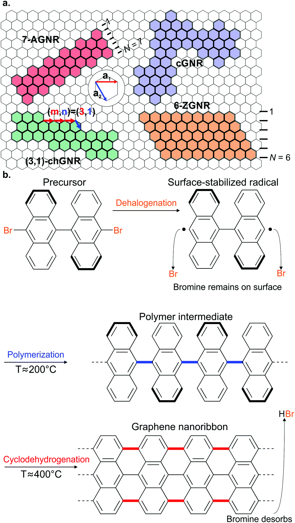 | ||
| Fig. 1 (a) Various GNR types and their classification. (b) Schematic overview of on-surface GNR fabrication for the case of a 7-AGNR. | ||
On the other hand, two parameters are required to uniquely identify chGNRs: their width and edge orientation. The edge orientation is determined by the number of graphene unit cell vectors, ma1 and na2, along the edge of the chGNRs unit cell (Fig. 1a).
There is no generally agreed upon classification scheme (although such a scheme has been proposed43) for cGNRs. cGNRs are GNRs with a meandering topology. They can possess a combination of armchair and zigzag edge terminations.
Since the seminal work of Cai et al.,37 who successfully fabricated the first atomically precise AGNR using on-surface synthesis, most GNRs have been synthesized using the same multistep process based on Ullmann-type coupling and cyclodehydrogenation. The first step involves the evaporation of a halogenated aromatic precursor on a well-defined (mainly single crystal) surface. Second, the halogen substituents are split off in a thermally-induced, surface-assisted Ullmann-type coupling reaction resulting in the formation of a polymer or metal–organic intermediate. Lastly, surface-assisted cyclodehydrogenation converts the polymer into a GNR with well-defined width and edge termination. Below, we will discuss the different steps involved in GNR on-surface synthesis.
Ullmann-type coupling
Ullmann coupling is a reaction where two aryl halides couple to form a biaryl, catalysed by Cu.44 The effectiveness of Ullmann-type coupling for the rational, bottom-up design of covalently coupled one- or two-dimensional nano-architectures on metallic substrates was shown in pioneering work by Grill et al.45 In the past few decades, Ullmann-type coupling has proven to be uniquely useful for the creation of surface-confined zero-dimensional clusters, one-dimensional (1D) chains and two-dimensional (2D) networks.46–48 For the specific purpose of synthesizing GNRs, Ullmann-type coupling is the most ubiquitous reaction for generating the polymer intermediate because it normally does not have side reactions and, if an appropriate molecular precursor is used, the polymer intermediate already has the correct geometry for subsequent cyclodehydrogenation.49 Ullmann-type coupling typically occurs in three distinct, time-separated steps: (i) dissociation of the halogen substituents, leaving a surface-stabilized radical (Fig. 1b), (ii) subsequent surface-confined diffusion of the radical and (iii) recombination of the radicals,37,49–53 forming a polymer intermediate. Below, we will discuss the design of the precursor and the role of both the substrate and substituted halogen.All precursors used so far are polycyclic aromatic hydrocarbons (PAHs) with at least two halogen substitutions. A large selection of precursors used so far, together with their resulting GNR structures, is given in Fig. 3. The simplest precursors are those with 2-fold rotational symmetry and halogen substitutions in a para position (Fig. 2, blue building blocks). These precursors lead to AGNRs with the same width as the precursor (e.g. the synthesis depicted in Fig. 2b) or a ribbon with periodic width modulation (e.g.79). Creating wider ribbons following this design strategy requires larger precursors which are more difficult to synthesize (e.g. synthesizing acenes higher than pentacene poses a significant challenge54) and might not even sublime due to increased mass and intermolecular interactions.55 To circumvent this issue, an effective strategy is to design the precursor such that steric hindrance favours/excludes the formation of certain bonds (e.g.11). Using such a design strategy, atomically precise 9-, 13- and 17-AGNRs have been successfully synthesized.56,57 In addition, steric hindrance has also been identified as a useful concept for the synthesis of cGNRs and chGNRs.
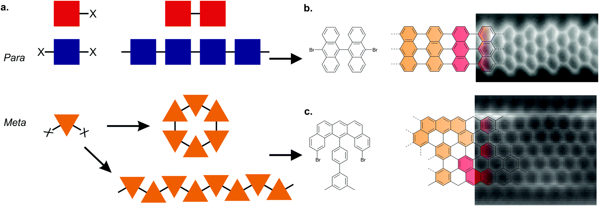 | ||
| Fig. 2 Precursor design determines the final product. (a) Schematic overview of the Ullmann coupling reaction in dependence of precursor design. X represents a halogen atom. Adapted with permission from ref. 49. Copyright 2017, the Royal Society of Chemistry. (b) Synthesis of a GNR from a precursor with halogen substitutions in opposite positions leading to an AGNR. The example depicts the formation of a 7-AGNR from dibromo-bianthryl together with a high-resolution non-contact (nc) atomic force microscopy (AFM) image recorded with a CO-functionalized tip. Adapted with permission from ref. 179. Copyright 2013, Springer Nature. (c) Synthesis of a GNR from a precursor having the halogens in the ‘meta’ position together with a high-resolution nc-AFM image recorded with a CO-functionalized tip. Steric repulsion prevents the formation of a cyclic nanographene. Adapted with permission from ref. 58. Copyright 2016, Springer Nature. | ||
Placing the halogen substitutions not on opposite ends of the precursor (e.g.50 and 65) can lead to the formation of a polymer with a zigzag structure (Fig. 2, orange building blocks). However, special care must be taken – for example by incorporating elements of steric hindrance – to prevent the formation of a cyclic nanographene. Using such design considerations, ZGNRs58 have been successfully synthesized (Fig. 2c), which are otherwise inaccessible as Ullmann-type coupling normally takes place along the armchair directions of graphene.
The use of prochiral precursors allows the fabrication of complex edge structures from relatively simple precursor molecules. In the case of homochiral coupling, the resulting GNR will be chiral (e.g.55 and 57) whereas in the case of heterochiral coupling, the resulting GNR will be achiral (e.g.42). However, a priori it is difficult to determine which coupling orientation will be preferred, which complicates the rational design using prochiral precursors.59 It should be noted that while the above discussed precursor design considerations allow for precise control over the width and edge orientation of GNRs, the precise control over their length remains a challenge which has not been solved until now.
During the second step (i.e. the diffusion of the surface stabilized radical) the substrate once again plays a vital role. For long-range ordered structures, a relatively high precursor mobility (i.e. a low diffusion barrier) is desirable, whereas the precursor reactivity should be low.60 Note that the on-surface reactivity of the precursor also depends on the catalytic activity of the substrate. A theoretical study of Björk et al.,52 using bromobenzene as a model molecule, showed that Cu(111) is the worst candidate of the three most commonly used (111)-oriented coinage metal surfaces in this respect since it has the highest diffusion barrier together with the largest catalytic activity. Interestingly, Ag(111) has a similar diffusion barrier as Au(111), but a lower catalytic activity making it the best surface for synthesizing highly ordered structures. In a combined experimental and theoretical study comparing Ag(111), Cu(111) and Au(111), using a sixfold iodine substituted cyclic precursor, Bieri et al.60 found similar results: the most well-ordered networks were formed on Ag(111), whereas the networks on Cu(111) were the least ordered. Nevertheless, Au(111) has remained the most widely used surface, also for GNR synthesis. When determining the right substrate for GNR synthesis another consideration has to be taken into account, namely the availability of metal adatoms originating from the metal surface. The surface-stabilized radicals left upon dehalogenation can – together with adatoms available from the metallic substrate – form metal–organic polymers which in some cases can67,68 and in other cases cannot59,68 be converted to GNRs. The energy required to generate adatoms on either Cu(111) or Ag(111) is less than on Au(111), i.e. adatoms are more abundant on the former two surfaces and thus, it is more likely to obtain metal–organic (intermediate) structures.69
Commonly, the (111)-oriented coinage metal surfaces have been used. However, the (110)-oriented coinage metal surfaces offer an anisotropic atomic arrangement with a row-like structure which provides the opportunity to guide the growth of GNRs. It nevertheless has to be considered that the synthesis is sensitive to the surface orientation as well. Using 10,10′-dibromo-9,9′-bianthracene (8) as a molecular precursor, a GNR could be readily formed on Cu(111),70–73 but on the more reactive74 Cu(110) substrate no GNR could be formed as the precursor bonded too strongly to the substrate.75 On Au(110), 8 can form a GNR, but owing to the lower mobility on this surface, the lengths of the formed GNRs were limited.76 A more successful strategy of aligning GNRs is to synthesize them on vicinal surfaces, such as Au(788) or Au(322).77–80 Because the terraces of these surfaces are Au(111) facets, results obtained on Au(111) can readily be replicated on Au(788), provided that the width of the GNR is not larger than the width of the terrace.
Lastly, the substrate material can influence how the precursors will couple to each other and that can even result in coupling schemes not intended for the designed precursor. For instance, on Au(111) 8 forms an AGNR as indicated in Fig. 1b37 whereas on Cu(111) it forms a chGNR with a combined armchair and zigzag edge (Fig. 3c) based on surface-assisted dehydrogenative coupling and not on Ullmann-type coupling.70–72
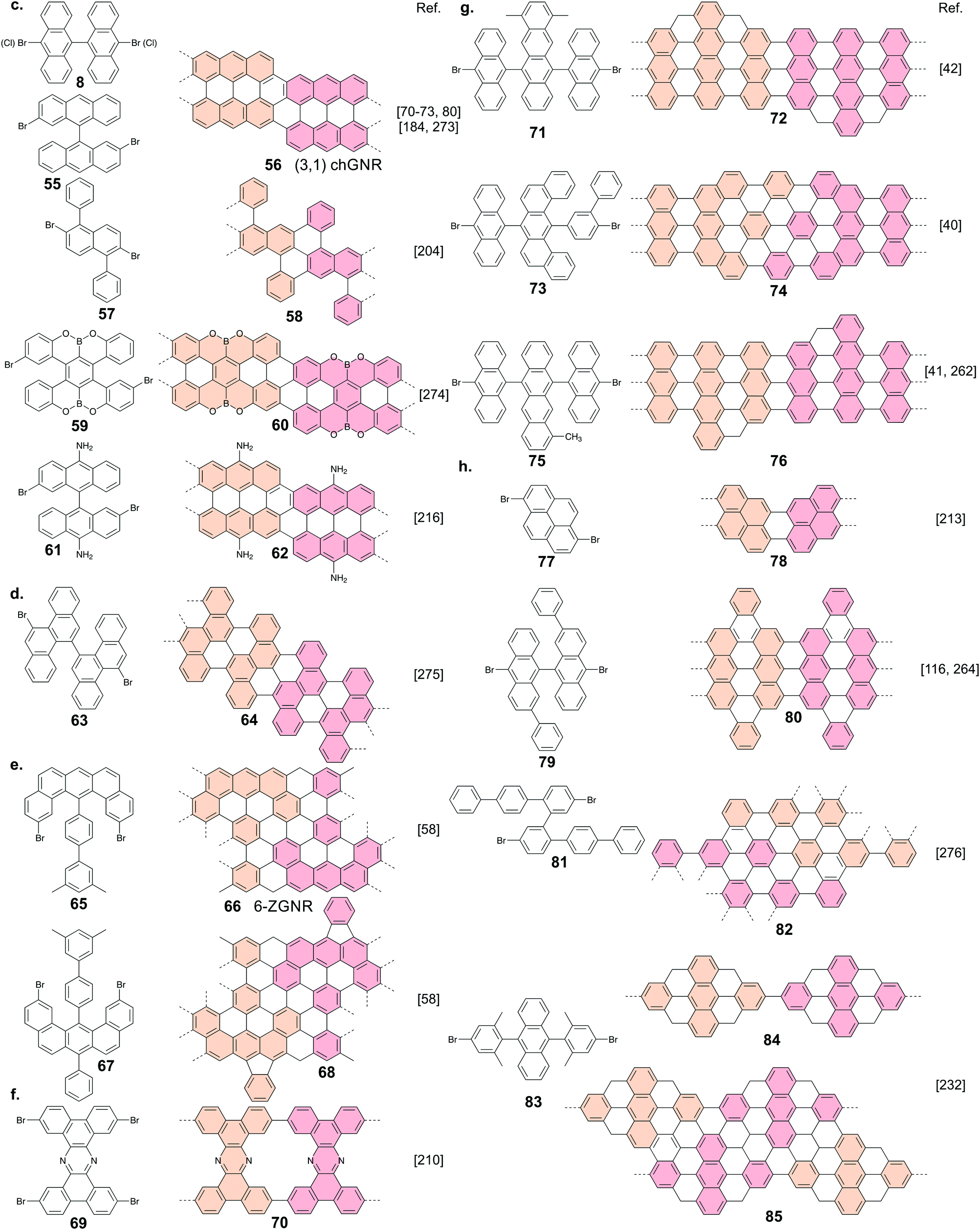 | ||
| Fig. 3 Register of precursors used so far for atomically precise GNR formation together with the resulting GNR structure. (a) Armchair GNRs, excluding ones resulting from the lateral fusion of ribbons. (b) Chevron-like GNRs. (c) Chiral GNRs. (d) Cove-edged GNRs, (e) zigzag GNRs. (f) Porous GNR. (g) GNRs with embedded topological states. (h) GNRs with other edge topology. | ||
The dissimilar amount of energy required for dehalogenation can be harnessed for hierarchical polymerization processes, where dissimilar halogen species are split off in a controllable, consecutive fashion, thereby allowing the formation of complex nano-architectures.83,87,88 An instructive example is the work of Bronner et al.,89 where a combination of iodinated and brominated precursors was used together with a ‘linker’ molecule, which had both an iodine and bromine substitution, to form GNR heterostructures with preferentially only a single junction per GNR. Without such hierarchical processes, the formation of GNR heterojunctions relies on stochastics and multiple junctions (of the same type) may form within a single ribbon.90–96
After the halogen bond has been cleaved, the split-off halogen can remain adsorbed on the surface. It has been suggested that the adsorbed halogens may hinder polymer growth,52,97 negatively affecting GNR quality. Typically the split-off halogens desorb upon cyclodehydrogenation as hydrogen halides, leaving pristine GNRs after the synthesis is completed.82,97,98 However, at that point the growth has already been negatively impacted. Adsorbed halogens can be removed by annealing, however this requires considerably higher temperatures than those required for the initial Ullmann-type coupling and is unfortunately also substrate dependent.52 A better option may be to dose H2,97,99,100 atomic hydrogen101 or Si102 which promotes the low-temperature desorption of halogens. Employing such techniques may help growing longer polymers and eventually GNRs, although care must be taken to avoid premature radical passivation with, for instance, hydrogen.103
Cyclodehydrogenation
The final step in GNR synthesis is the conversion of the polymer intermediate into a GNR through surface-assisted cyclodehydrogenation (Fig. 1b). Through cyclodehydrogenation, intramolecular aryl–aryl coupling occurs upon release of atomic hydrogen from the aryl units. Thereby, extra C–C bonds are formed and often a planarization of the molecule takes place. Although the experimental use of this reaction is abundant, relatively little theoretical work has been carried out with respect to the reaction mechanism.93,104,105The hydrogen released during the cyclodehydrogenation step was found to end ribbon growth by passivating the radical termini of the ribbons. Thus, after cyclodehydrogenation took place the ribbon can no longer increase in length.103
The requirement for the surface to be sufficiently catalytically active for cyclodehydrogenation to occur was demonstrated by the work of Kolmer et al.65 While 8 can polymerize through Ullmann-type coupling on the TiO2(011)-(2 × 1) surface, it cannot undergo cyclodehydrogenation as it does on Au(111).37 In recent work it was found that by strategically using fluorine substitutions (7) one can form nanographenes and GNRs on TiO2 through C–F bond activation, eliminating the need for a catalytically active substrate.109,110 This represents a milestone in the on-surface synthesis of GNRs, as growing GNRs directly on semiconducting or insulating surfaces foregoes the need for transfer when incorporating the ribbons in devices.
Electronic properties of graphene nanoribbons
As graphene is a gapless semimetal, it is unsuitable for applications for which a band gap is required, such as field effect and optoelectronic devices. As such, the principal interest in GNRs is their semiconducting behaviour caused by quantum confinement of the charge carriers. However, GNRs also host a plethora of rich electronic behaviours depending on their width and edge termination. For instance, AGNRs have width-dependent band gaps,6,29,118,119 whereas ZGNRs are expected to host spin-polarized edge states,29,119,120 making them promising candidates for spintronic applications. On the other hand, cGNRs, with meandering topology, are expected to be more suitable for thermoelectric and optoelectronic applications than their straight counterparts.121–127 Moreover, the excellent control over their structure provided through on-surface synthesis has been harnessed to create engineered topological states, which received increasing attention in both theoretical128–131 and experimental studies.40–42Subsequently, we will discuss the fundamentals of the electronic properties of different GNRs, as well as the experimental characterization of them.
Theoretical background
Due to the finite width of GNRs, the electron momenta are quantized in the transverse ribbon direction. An illustrative and intuitive way to approximate the band structure of GNRs is to start with the well-known tight-binding band structure of graphene and to make cuts along the allowed momentum values (Fig. 4a). In this way, a 1D band structure is formed out of the obtained conic sections. This approach is analogous to that employed for carbon nanotubes and the results are similar, too.132 Based on this approach, AGNRs can be divided into three classes: N = 3p, N = 3p + 1 and N = 3p + 2 where p is a natural number and N denotes the number of dimer lines along the edge, i.e. the width of the GNR (Fig. 1a). The AGNRs belonging to the 3p + 2 family are found to be semimetallic within this approximation, whereas the ribbons of the other two families are semiconducting.6,119,120 From LDA-DFT calculations, it has been found that all GNRs of finite width are semiconducting, including AGNRs belonging to the 3p + 2 family (Fig. 4b).29 The hydrogen passivation of the edges plays an important role in the opening of a band gap in the 3p + 2 family, as the hydrogen atoms change the on site energy of the outer carbon atoms compared to the inner ones and consequently the bond lengths at the edges are altered. When this alteration is taken into account within the tight-binding model, the 3p + 2 family is then also semiconducting.29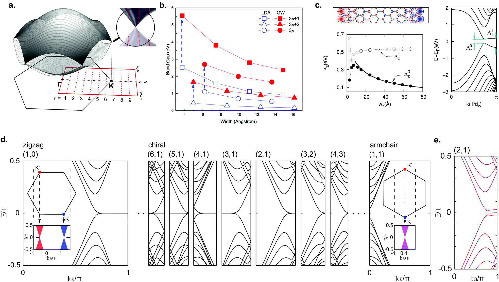 | ||
| Fig. 4 Electronic properties of graphene nanoribbons. (a) Formation of the band structure of GNRs by selecting cuts along allowed k-values for a 9-AGNR. Reprinted with permission from ref. 57. Copyright 2017, American Chemical Society. (b) LDA-DFT calculations of AGNR band gaps and quasiparticle correction. Reprinted figure with permission from ref. 118. Copyright 2007 by the American Physical Society. (c) Electronic structure of ZGNRs from LSDA-DFT calculations, showing the spin-polarized edge state, formation of a band gap and band gap as a function of ribbon width. Reprinted figure with permission from ref. 29. Copyright 2006 by the American Physical Society. (d) Band structure of various zigzag, chiral and armchair GNRs from tight-binding calculations. Reprinted figure with permission from ref. 135. Copyright 2011 by the American Physical Society. (e) Mean-field Hubbard model calculations for a (2,1) chiral GNR, showing the opening of a band gap. Reprinted figure with permission from ref. 135. Copyright 2011 by the American Physical Society. | ||
For ZGNRs, a flat band at the Fermi level, corresponding to an edge state that decays exponentially into the ribbon, arises from tight-binding calculations.6,120 The high DOS at the Fermi level originating from this flat band is expected to lead to a spin-polarization through electron–electron interactions, opening a band gap.119 Indeed, the Hubbard model and LSDA-DFT calculations predict a magnetic insulating ground state for ZGNRs.29,119,120,133 The spins are ferromagnetically ordered along one edge and antiferromagnetically coupled between edges (Fig. 4c). A band gap (Δ0) arises that is related to antiferromagnetic correlation between the two edges, whereas Δ1 is related to the ferromagnetic correlation along the edges.134 As the ribbon gets wider Δ0 decreases, similar to AGNRs, whereas Δ1 remains constant.29,118
With on-surface synthesis, GNRs with arbitrary edge structure can be synthesized. Two of the most common ribbon types with alternating edge topologies are the cGNR and chGNR. A chGNR can be defined by three variables: its width and the numbers m and n of the graphene unit cell vectors a1 and a2, respectively, within one ribbon unit cell (Fig. 1a). Using this description, (m,n) = (1,0) corresponds to a ZGNR, while (1,1) corresponds to an AGNR. Without considering electron–electron interactions, chGNRs having a structure close to the one of ZGNRs, i.e. those with a large amount of zigzag edges within a unit cell, exhibit flat band dispersion similar to ZGNRs, whereas for chGNRs close to AGNRs the flat band is almost completely suppressed (Fig. 4d).6,135 When electron–electron interactions are taken into account, a band gap opens for all chGNRs (Fig. 4e).28,135–137 The band gap of chGNRs, similar to AGNRs, decreases with increasing width, but not monotonically.28,137–139
cGNRs are meandering GNRs with a periodic edge structure. The edge orientation can be exclusively armchair, zigzag or a combination of both. The electronic properties of these ribbons were extensively studied with the Hubbard model, DFT and the many-body GW approach.43,140,141 Interestingly, all ribbons with a zigzag edge are expected to exhibit an antiferromagnetic ground state, which should survive on Au(111) according to DFT calculations.141
Direct comparison of theory with experimental values is difficult. In a typical experiment used to probe the electronic properties of GNRs, e.g. (angle-resolved) photoelectron spectroscopy (ARPES) or scanning tunneling spectroscopy (STS), one does not directly measure the electron energy levels. Instead, charged excitations are measured resulting from the addition or removal of electrons during the measurements. Thus, care has to be taken when comparing experimental data to calculations based on non-interacting particles (e.g. tight-binding and DFT). In the specific case of GNRs, e–e interactions play an important role due to the weak screening and GNRs’ (quasi-)1D nature.78,118,142–144 Using one-shot G0W0 calculations the quasiparticle gaps grow significantly when compared to single particle techniques like DFT (Fig. 4b).118 Lastly, the substrate plays a significant role through enhanced screening, lowering the quasiparticle bandgap when compared to an isolated ribbon. By combining G0W0 together with a semiclassical image-charge model good agreement between experiment and theory has been found.78,127,144,145
The possibility of quasiparticle-mediated charge transport – notably through polarons – has been extensively studied on the tight-binding level of theory.155–165 It was found that stable polarons might form in narrow (N ≤ 8) AGNRs.157 In addition, interactions of these polarons with defects have been investigated and it was found that while some defects fully transmit polarons, others can reflect them.158,164
For implementing GNRs in devices, not only the intra-ribbon transport is important but also the inter-ribbon transport (ribbon–ribbon hopping), since the length of the channel will typically be larger than the length of a single GNR. Richter et al.166 employed a model previously successfully applied to organic semiconducting thin films167,168 to correctly describe the behaviour of GNR thin film devices. For such devices they found that the limiting factor for charge transport is the inter-ribbon hopping.79,166
Experimental characterization of GNRs
The narrowest possible GNR is the 3-AGNR, which is a poly(p-phenylene) (PPP) wire. Unlike wider GNRs, PPP wires are non-planar and do not feature the same delocalized π-system as wider AGNRs. Up to now, PPP wires have been synthesized on Cu(110), Au(111) and vicinal Au(322).80,111,112,169,170 The band gap of these wires adsorbed on Au(111) was reported to be between 3.05 and 3.23 eV.80,112 However, the principle interest in PPP wires has been in the creation of 3p (medium-Δ) GNRs through lateral fusion (Fig. 5a). In this way, 6-, 9-, 12- and 15-AGNRs were obtained. Their characterization with STS112 yielded values for the band gaps of 1.69 eV, 1.35 eV, 1.13 eV and 1.03 eV, respectively. Note that, although the 9- and 15-AGNRs were synthesized using other precursors as well,57,171 at the time of writing the 6- and 12-AGNR remain inaccessible through other means.
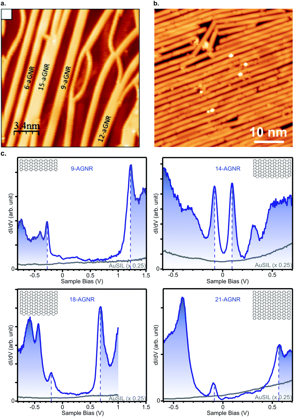 | ||
| Fig. 5 (a) Lateral fusion of poly(p-phenylene) wires leads to formation of 3p-AGNRs. Reprinted with permission from ref. 112. Copyright 2017, American Chemical Society. Provided under an ACS AuthorChoice License, requests for further permissions should be directed to the American Chemical Society. (b) Long 9-AGNRs formed on Au(111) from an iodine functionalized precursor. Reprinted with permission from ref. 82. Copyright 2017, American Chemical Society. (c) STS spectra for 9-, 14-, 18- and 21-AGNRs on Si/Au(111) from which the band gap can be determined. Reprinted with permission from ref. 114. Copyright 2017, American Chemical Society. | ||
The 5-AGNR is the narrowest in the small-Δ family of GNRs and is well-researched. The reported values for the band gap of the 5-AGNR differ significantly. The first time it was fabricated, by Zhang et al.,67 its band gap was identified as 2.8 eV with STS. This is significantly larger than the value of 1.32 eV which was obtained for isolated 5-AGNRs with many-body GW calculations. This discrepancy was explained by the hybridization of the GNRs with the Au(111) surface. Later, Kimouche et al.172 carried out a systematic study of the band gap versus ribbon length and identified additional orbitals which appeared less prominent in STS experiments and found a band gap of 100 meV for 5-AGNR on Au(111). Similar results were found by Zdetsis and Economou173 who found with time-dependent DFT that the band gap of long (>10 nm) ribbons is close to 100 meV. Recently, Lawrence et al.174 reported a band gap of 0.85 eV for the 5-AGNR on Au(111) and additionally identified two topological end-states (see also the theoretical work of Cao et al.129). The end-states only appear when the ribbon is sufficiently long (>16 unit cells, on shorter ribbons the end-states hybridize into a bonding and anti-bonding orbital and are delocalized over the ribbon). Since Kimouche et al.172 only report data for ribbons up to a length of 14 unit cells, it is feasible that what they identified as the valence and conduction band are the end-states identified by Lawrence et al.174 On Ag(111), the band gap of the 5-AGNR was reported to be 1.3 eV.68 Note that the surface also has some influence on the band gap of adsorbed GNRs.144,145
The first-ever synthesized and most well-researched GNR is the 7-AGNR. In addition, it is the narrowest GNR in the large-Δ family that has been synthesized so far. 7-AGNRs were synthesized from 8 on Au(111),37 Ag(111),113 and TbAu2/Au(111)175 and recently on TiO2(011)-(2 × 1)109 from 7. Its properties have been extensively studied with a myriad of techniques: with STS,78,109,113,114,175–182 Fourier transformed (FT-)STS,180,182 (angle-resolved) photoelectron spectroscopy (ARPES),77,78 X-ray photoelectron spectroscopy (XPS),183,184 Raman spectroscopy,37,113,185,186 UV-vis spectroscopy,185 two-probe conductance measurements,73,177,178 high-resolution electron energy loss spectroscopy (HREELS),187 (angle-resolved) two-photon photoelectron spectroscopy,187,188 inverse photoemission spectroscopy (IPE),77 reflection difference spectroscopy (RDS)189 and STM induced light emission experiments.177 The band gap of 7-AGNRs measured with STS range from 2.3 eV to 2.7 eV78,109,114,175,176,178,180,182 which is in good agreement with theory. Similarly, with HREELS, 2PPE and IPE the band gap of 7-AGNRs was found to be in the range of 2.6 to 2.8 eV.77,187,188 Note that the band gap depends somewhat on both the end termination of the ribbons (CH or CH2) and their length, especially for short (<8 nm) ribbons.103,176 With RDS, the optical gap of aligned 7-AGNRs was determined by Denk et al.189 to be 2.1 eV. For the case of optical excitation, the gap is reduced compared to GW calculations by the exciton binding energy whereas the surface plays a less dominant role than in the case of charged excitations (e.g. dI/dV point spectroscopy experiments).190
By aligning 7-AGNRs with the help of a vicinal substrate,77,78 the band structure of the occupied states can be examined. With ARPES the effective mass was determined to be mVB = 0.21–0.23 me78,191,192 and mVB = 1.07 me77 and the charge carrier velocity to be v = 8.2 × 10⁵ m s−1 (Fig. 6a).78 The effective masses found with AR-2PPE on randomly-oriented ribbons is mVB = 1.37 me for the valence band and mCB = 1.35 me for the conduction band.188 In FT-STS193,194 standing wave patterns caused by the diffraction of electrons are investigated by recording multiple STS point spectra along the length of a ribbon. In this way, the dispersion of individual GNRs can be obtained. Using this technique, effective masses of mVB = 0.41 me and mCB = 0.40 me were found for 7-AGNR on Au(111)182 and mVB = 0.32 me and mCB = 0.35 me on a decoupling NaCl layer (Fig. 6b).180 Obviously, the measured effective masses vary substantially. The origin of this effect was resolved by Senkovskiy et al.195 who found that the (first) valence band of aligned 7-AGNRs can only be observed with ARPES in a narrow range of emission angles. When the appropriate emission angle was chosen, the valence band was observed and an effective mass mVB = 0.4 me was obtained in excellent agreement with the FT-STS results. The result of mVB ≈ 0.2 me occurs when the second valence band is mistaken for the first one. The massive fermion behaviour of charge carriers in GNRs is a direct consequence of the opening of a band gap and GNRs with smaller band gap should thus have lower effective masses.78 This can be qualitatively understood from the ‘cutting scheme’ (Fig. 4a) described earlier: if the frontier cut is close to the Dirac point the resulting conic section will be ‘sharper’ and consequently the charge carriers have lower effective mass.
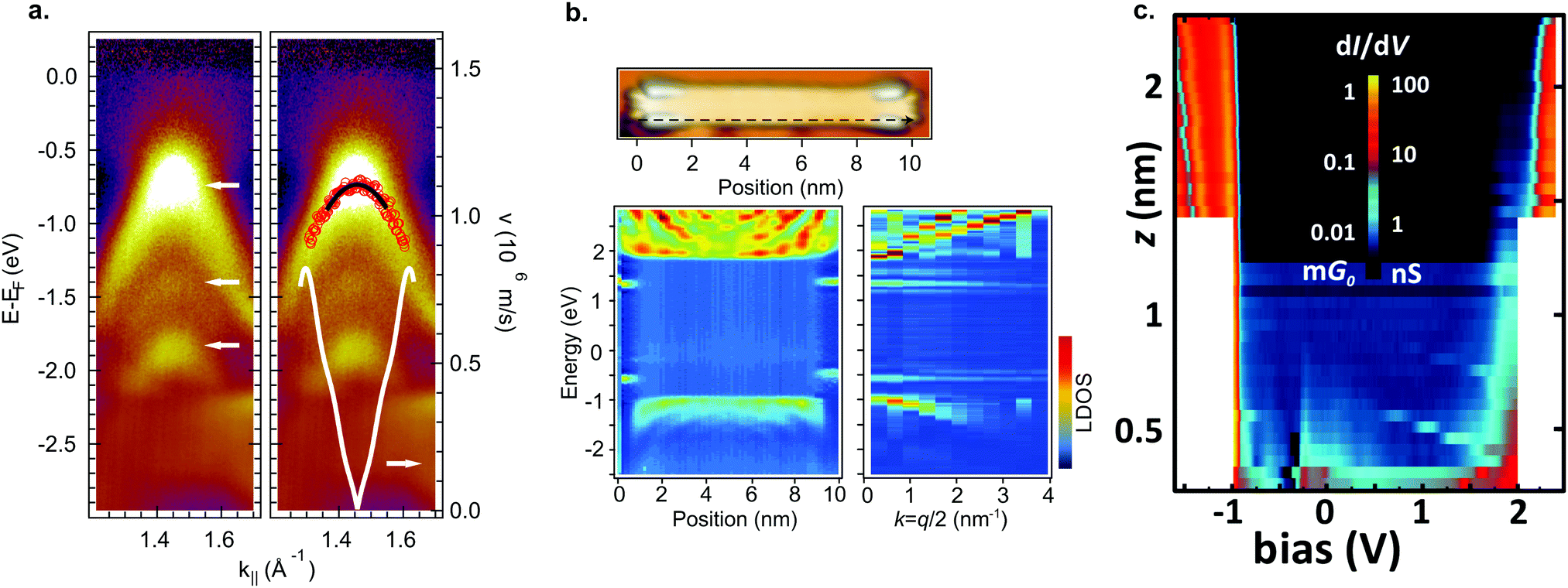 | ||
| Fig. 6 Electronic properties of 7-AGNRs. (a) ARPES data of aligned 7-AGNRs on Au(788). In the left panel 3 dispersive bands are marked by white arrows. The right panel shows a parabolic fit (black line) from which mVB = 0.21 me is extracted. The white curve indicates the carrier velocity. Reprinted with permission from ref. 78. Copyright 2012, American Chemical Society. (b) FT-STS for 7-AGNR on a monolayer NaCl on Au(111). The bottom left panel shows STS spectra taken along the black dashed line indicated in the top image. Bulk as well as end states are visible. The bottom right panel shows the Fourier transform of the bottom left panel. Dispersive bands around −1 eV and +2 eV are visible, as well as two non-dispersive bands around −0.5 eV and +1.4 eV corresponding to the end states. Adapted with permission from ref. 180. Copyright 2016, the Authors, published by Springer Nature. Provided under a Creative Commons CC BY 4.0 international license. (c) Conductance map for 7-AGNR on NaCl on Au(111). For small (<∼0.5 nm) tip-sample distances, there is some in gap, non-resonant tunneling present. At larger tip-sample distances, only resonant tunneling can be observed. Adapted with permission from ref. 73. Copyright 2018, American Chemical Society. | ||
In addition to the delocalized valence and conduction electrons, 7-AGNRs (at least those obtained from 8) host localized end states at their termini which are associated with the local zigzag edge orientation.6,103,176–180 These end states are predicted to be spin-split, but for 7-AGNRs on Au(111) they were observed in STS experiments as a single peak, which is possibly degenerate due to hole-doping, close to the Fermi level.179 However, for 7-AGNR adsorbed on NaCl, the zigzag end states are reported to split and a gap between them of 1.9 eV is opened. In line with the localized nature of these states, they are found to be non-dispersive with FT-STS (Fig. 6b).
By picking up a 7-AGNR with an STM tip, a two-probe conductance experiment can be performed.196 As the tip-sample distance L increases, the conductance is expected to decay as exp(−β(V)L) where β(V) is the conductance decay parameter.73,196 When the applied bias is equal to a molecular energy level of the ribbon, β decreases giving rise to resonant tunneling (Fig. 6c).73,178 The end states only provide a contribution to tunneling at small tip–sample distances due to their localized nature. Note that in this geometry (a part of) the ribbon is decoupled from the surface which leads to an alteration of their electronic properties compared to their adsorbed counterparts.
By lateral fusion of 7-AGNRs, both 14- and 21-AGNRs were obtained on Au(111) and Ag(111).113,114 A band gap of 0.2 eV and 0.7 eV, respectively, was obtained from STS on Si/Au(111)114 (Fig. 5c). The larger gap for 21-AGNRs can be qualitatively understood since they belong to the medium-Δ family, whereas the narrower 14-AGNR belongs to the small-Δ family.
On the other hand, by lateral fusion of either 5-AGNRs or 7-AGNRs with a PPP wire, 8-AGNRs or 10-AGNRs were formed on Au(111).197 The band gap of these ribbons was measured to be 1.0 eV and 2.0 eV, respectively. The value for the 8-AGNR presents a departure from the general trend that as the band gap decreases the wider the ribbons get, as the band gap for the smaller 5-AGNR, which belongs to the same (small-Δ) family, was determined to be 0.85 eV.174
The third and most well-researched AGNR in the medium-Δ family, the 9-AGNR, can be synthesized by clever use of steric hindrance from 11 on Au(111) (Fig. 5b).57 Its band gap is 1.4 eV on Au(111)57 and 1.5 eV on Si/Au(111) (Fig. 5c).114 With ARPES the effective mass mVB = 0.09 me was found, whereas with FT-STS mVB = 0.12 me and mCB = 0.11 me were obtained.57 Compared to the 7-AGNR, this is in agreement with the prediction that GNRs with narrower band gaps have lower effective charge carrier masses. Two fused 9-AGNRs forming an 18-AGNR were reported to exhibit a band gap of 0.9 eV on Si/Au(111) (Fig. 5c).114
The 13-AGNR, synthesized from 14, is the second-ever AGNR synthesized with atomic precision. Its band gap, determined with STS, is 1.4 eV on Au(111) and it has a localized, in-gap end state originating from the zigzag edges at its terminus.198 Recently, the 13-AGNR was also synthesized from 16 by Yamaguchi et al. on Au(111).56 This leads to a ribbon with identical interior, but notably with a different edge orientation at the termini. They reported a similar band gap of 1.34 eV. However, they reported no end state for their ribbons. In addition, using FT-STS they found effective masses of mCB = 0.14 me and mVB = 0.13 me.
Lastly, the widest GNR, which has been so far fabricated with atomic precision, is the 17-AGNR. It has a small band gap of 0.19 eV on Au(111) and with FT-STS an effective mass mCB = mVB= 0.06 me was found.56
From the experimental characterization of AGNRs, the three predicted Δ families become apparent in accordance with theory. When selecting AGNRs for devices, a tradeoff has to be made between band gap and effective mass, where wider band gaps lead to larger effective carrier masses and therefore, lower electron mobility. Conversely, AGNRs with narrower band gaps will have higher electron mobilities.
![[double bond, length as m-dash]](https://www.rsc.org/images/entities/char_e001.gif) C) can undergo lateral fusion. In contrast, only a single type of atomically precise nanoporous graphene forms in this case (Fig. 7b).117
C) can undergo lateral fusion. In contrast, only a single type of atomically precise nanoporous graphene forms in this case (Fig. 7b).117
 | ||
| Fig. 7 (a) nc-AFM image of an edge extended cGNR synthesized from 46. Reproduced with permission from ref. 201. Copyright 2019, Wiley-VCH. (b) Nanoporous graphene from lateral fusion of cGNRs using 38 (X = C) as a precursor. Reprinted with permission from ref. 117. Copyright 2020, American Chemical Society. (c) Nitrogen and boron doped chevron-like GNRs with partial zigzag edges fabricated from precursors 48 (right) and 50 (left). Reproduced with permission from ref. 203. Copyright 2020, the Authors, published by Wiley-VCH. Provided under a Creative Commons CC BY 4.0 international license. (d) Formation of (3,1)-chGNRs on Cu(111) based on the suggested synthesis of Sánchez-Sánchez et al. (ref. 72). (e) nc-AFM image of a (3,1) chiral GNR formed from 9,9′-bianthracene (8 without halogen substitutions) on Cu(111). Reprinted with permission from ref. 208. Copyright 2017, American Chemical Society. (f) dI/dV maps of the valence and conduction band of the (3,1) ch-GNR on Au(111). Reprinted with permission from ref. 209. Copyright 2017, American Chemical Society. (g) dI/dV maps of (3,1)-chGNR on NaCl. The top row reports the simulated data and the bottom row the experimental data. Reprinted with permission from ref. 73. Copyright 2018, American Chemical Society. | ||
In addition, the synthesis of further cGNRs has been successfully achieved. For instance, two heterodoped GNRs were fabricated by Fu et al.203 on Au(111) from the two similar precursors 48 and 50. Both GNRs are doped with nitrogen and boron. The electronic band gaps of GNRs 49 and 51 (Fig. 7c) were determined to be 1.5 eV and 0.9 eV, respectively. These cGNRs are unique in the sense that they are the only ones so far with a partial zigzag edge topology.
By using prochiral precursors, cGNRs can be created from relatively simple precursors. For instance, the delicate interplay of precursor and substrate led to the formation of the heterochiral GNR 42 on Au(111), a narrow cGNR.59
The theoretically predicted unique properties of cGNRs – besides the determination of their band gaps – have not been experimentally verified thus far. For instance, due to the lack of cGNRs with pristine zigzag edges, the predicted anti-ferromagnetic ground state of those cGNRs could not be verified.43
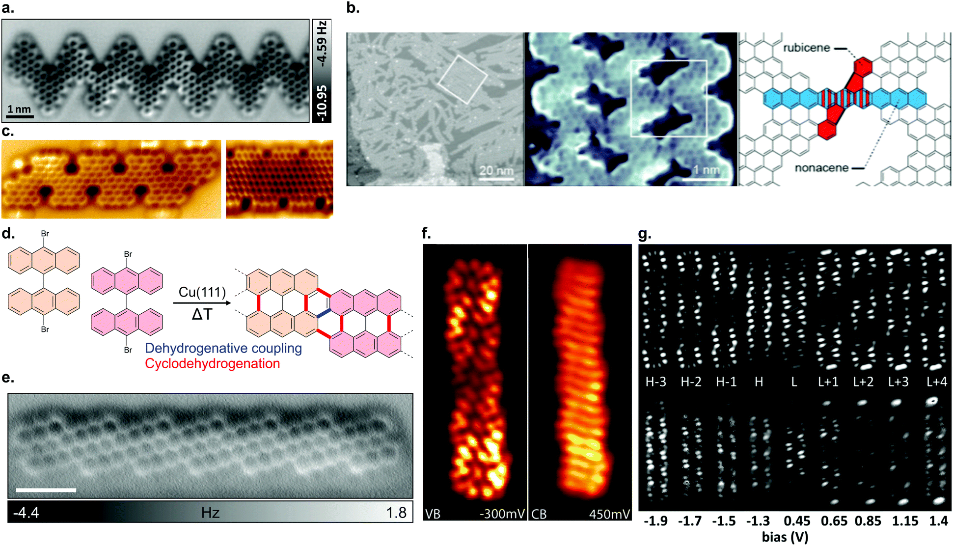
The formation of (3,1)-chGNRs from 8 on Cu(111) (Fig. 7d) was controversial with respect to the ribbon structure when the first reports appeared.71,205–207 With the help of nc-AFM imaging, the formation of a (3,1)-chGNR could be confirmed.72 It should be noted that 8 forms a 7-AGNR on Au(111). The formation of (3,1)-chGNRs from halogen-functionalized bianthryl precursors presents an exception: the formation is not based on Ullmann coupling but rather on a surface-assisted dehydrogenative coupling (blue bond in Fig. 7d).70–72,184,208 Indeed, 9,9′-bianthracene, without any halogen substitutions, forms a (3,1)-chGNR on Cu(111) as well (Fig. 7e).72,208
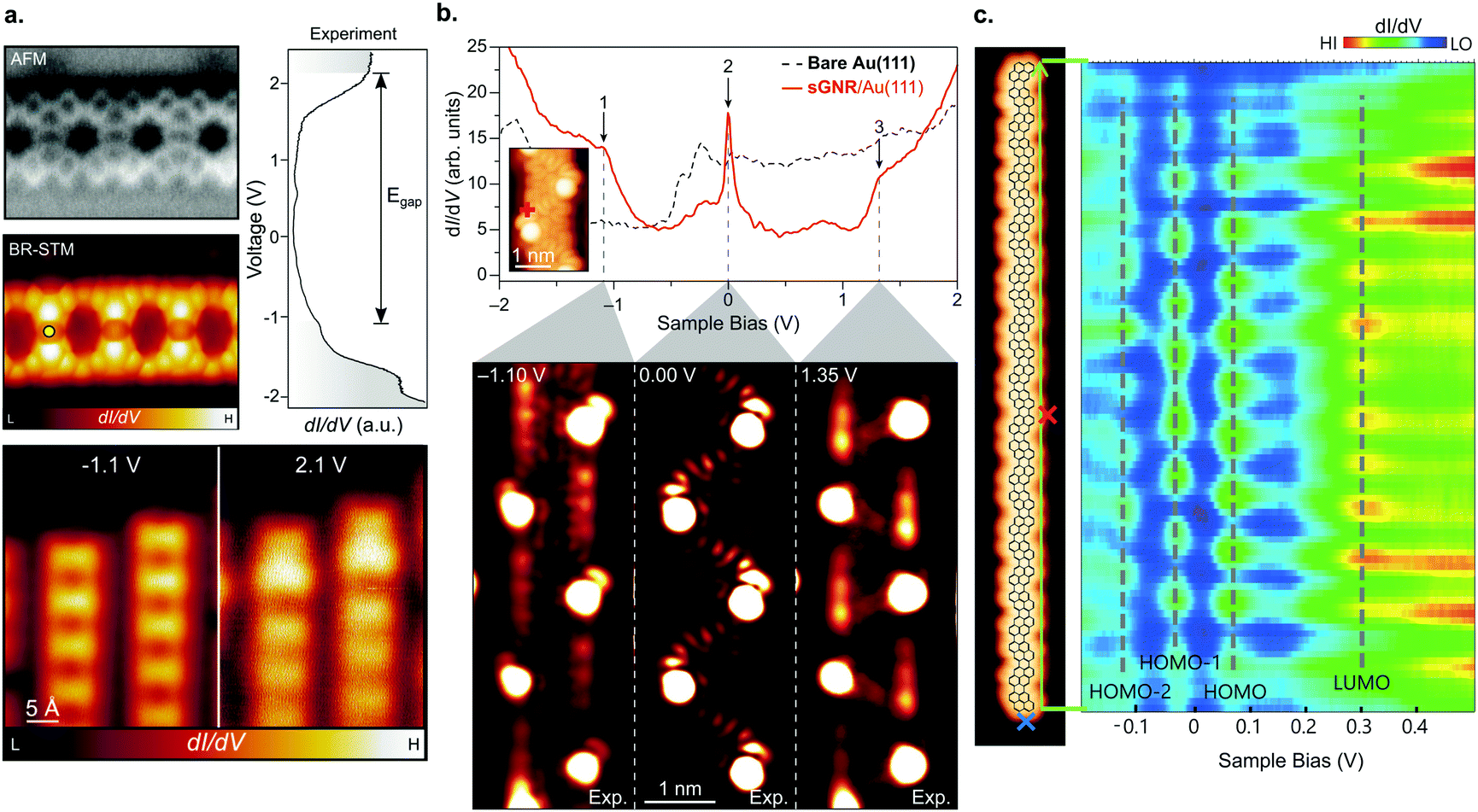
With STS, the band gap of (3,1)-chGNRs on Au(111) was determined to be 0.67 eV (to form (3,1)-chGNRs on Au(111) 55 must be used as a precursor).209 The spatial distribution of the valence and conduction bands is shown in Fig. 7f. The charge carriers have an effective mass of mVB = 0.34 me and mVB = 0.36 me obtained with FT-STS and ARPES, respectively, in good agreement with DFT calculations.209 Comparing this to the 7-AGNR, which has a comparable width, the effective masses are similar (the effective mass for the 7-AGNR is mVB = 0.41 me and mVB = 0.4 me obtained with FT-STS182 and ARPES195 respectively). However, the band gap of the 7-AGNR is much wider, approximately 2.4 eV.182 Thus, the trend that in the case of AGNRs narrow band gaps lead to lower effective masses does not hold for GNRs with more complicated edge structures. By decoupling the (3,1)-chGNR from the metallic substrate with a layer of NaCl, the electronic properties of the ribbon changed dramatically. The band gap widened to 1.8 eV and the electronic orbitals became more localized on the edges of the ribbon (Fig. 7d).73 Changes of this magnitude were not observed for AGNRs (compare for instance a 7-AGNR, which has a band gap of ∼2.4 eV on Au(111) and ∼2.9 eV on NaCl).180 A possible origin may lie within the stronger interaction of zigzag edges with the metal substrate (as compared with armchair edges), which was also observed for the 6-ZGNR.58
Although the predicted spin-split edge states have been observed for chGNRs originating from the chemical unzipping of CNTs,19 such results have not yet been found for bottom-up synthesized chGNRs.
 | ||
| Fig. 8 GNRs with unconventional topologies. (a) Porous GNRs (70) hosting a regular array of vacancies. High-resolution nc-AFM und STM images (left), together with their electronic structure (right). Reprinted with permission from ref. 210. Copyright 2020, American Chemical Society. (b) Electronic structure of sawtooth GNRs (76) revealing a zero-mode band at the Fermi level (marked with 2 at 0 V). The red spectrum (top image) was taken at the position indicated in the inset. The three lower images display the dI/dV maps recorded at the energies indicated by arrows in the top image. From ref. 41. Reprinted with permission from the American Association for the Advancement of Science. Copyright 2020, the Authors. (c) Electronic properties of pyrene-based GNRs (78) (STM image to the left) revealing their narrow band gap (line spectra to the right, taken along the green arrow given in the STM image). Reproduced with permission from ref. 213. Copyright 2020, Wiley-VCH. | ||
Another recent advancement in the field attracting considerable attention is the formation of engineered topological states in GNRs.40–42 The ribbons created up to now (Fig. 3f) have focused on what can be interpreted as periodically repeating 7–9 AGNR heterojunctions. Depending on the boundary region, the 7- and 9-AGNR sections may belong to inequivalent topological classes leading to the formation of topological interface states.129 This can be harnessed to introduce topologically derived in-gap bands (Fig. 8b).40–42
GNRs of unconventional shape may also be used to further tune the electronic properties of GNRs. For instance, pyrene GNRs (78) have a remarkably narrow band gap of Eg = 0.12 eV (Fig. 8c) and the lowest effective charge carrier masses mVB = mCB = 0.02 me reported up to date.213 This is an even narrower gap than the one reported for the 5- and 8-AGNRs which belong to the small-Δ family.
Edge doping (i.e. the dopant atoms are situated on the ribbon edges, such as in structures 35 and 37) with nitrogen atoms almost does not change the band gap compared to undoped ribbons, but it causes a downshift of 0.1 eV per nitrogen atom present in the precursor molecule of both the valence and conduction band (Fig. 9a).39,96 On the other hand, cyano-functionalization of 7-AGNR (27) was shown to narrow the band gap by 0.1 to 0.2 eV due to the extension of the π-system with an extra carbon atom. Since some CN moieties split off during the reaction, regions with both one and two cyano groups per unit cell were found in the ribbons. A rigid downshift of 0.2 to 0.3 eV per CN group present in the precursor was observed,214 much more than the shift per nitrogen atom for edge doping. Thus, not only the heteroatom species, but also the binding motif is important for tuning the GNR electronic properties through doping.
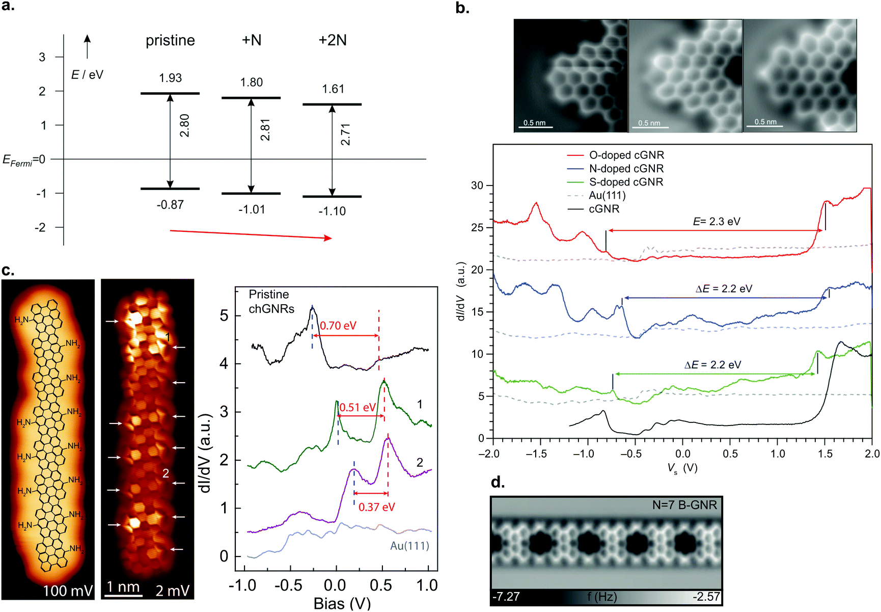 | ||
| Fig. 9 (a) Summary of band alignment of nitrogen doped cGNRs on Au(111) investigated by a combination of HREELS and UPS. Pristine (2N) corresponds to 30 (34), while 1N corresponds to a monomer with one pyridyl group. Reproduced with permission from ref. 39. Copyright 2013, Wiley-VCH. (b) Doping of cGNRs with (left to right) NH, O and S. The nc-AFM images detail the different appearances (left) while the right panel displays the respective STS spectra in comparison to a pristine cGNR. cGNR (doped cGNR) corresponds to 31 (39) in Fig. 3. Adapted with permission from ref. 200. Copyright 2017, American Chemical Society. (c) From left to right: STM image of an NH2 doped (3,1)-chGNR with overlaid structure model. Same area imaged with a CO-functionalized tip. STS spectra taken at the positions indicated in the STM image. Reprinted with permission from ref. 216. Copyright 2020, American Chemical Society. (d) nc-AFM image of a boron doped 7-AGNR. The boron substitutions appear dark in the image. Reproduced with permission from ref. 219. Copyright 2015, the Authors, originally published by Springer Nature. Provided under a Creative Commons CC BY 4.0 international license. | ||
Note that for the geometries of the above discussed GNRs the nitrogen atoms’ lone pairs are orthogonal to the extended π-system of the GNR. By using heteroatoms such that their lone pair overlaps with the extended π-system, the band gap of GNRs can be tuned, as well.200,215 For instance, cGNRs with either NH or O or S functionalization (39) have their band gap altered by approximately 0.2 eV compared to a pristine cGNR (31) (Fig. 9b).200 A recent study conducted by Li et al.216 showed that edge functionalization can even act to partially depopulate the valence band through hole doping (Fig. 9c).
In addition to edge doping, heteroatoms may be placed on the inner part of the ribbon. In this case, the heteroatoms must conform to a trigonal planar structure to fit with graphene's geometry. This has only been applied in two structures so far: 23 and 25. In 23 (Fig. 9d), the empty boron pz orbitals hybridize with the extended π-system of a 7-AGNR, leading to the formation of in-gap dopant bands with a band gap Eg = 1.2 eV.217–219 Thus, the electronic properties of B-doped 7-AGNRs are significantly altered with respect to their pristine counterpart.
So far we considered heavily doped GNRs, with dopant concentrations far exceeding those in conventional semiconductors. By mixing undoped and doped precursors, a more dilute doping regime can be achieved.218,220 Individual boron dimers were recently found to induce π-paramagnetism in 7-AGNRs due to the local disruption of its extended π-system.221 A summary of the electronic band gaps and effective masses of the discussed GNRs is given in Table 1.
| Precursor | Ribbon type | Band gap | Effective mass |
|---|---|---|---|
| a See discussion in article text. | |||
| 1, 3 | 3-AGNR | 3.05 eV,80 3.23 eV112 | |
| 4, 5 | 5-AGNR | 2.8 eV,a![[thin space (1/6-em)]](https://www.rsc.org/images/entities/char_2009.gif) 67 1.3 eV,68 0.85 eV,174 0.1 eV172 67 1.3 eV,68 0.85 eV,174 0.1 eV172 |
|
| 3 | 6-AGNR | 1.88 eV,80 1.69 eV112 | 0.15 me80 |
| 7, 8 | 7-AGNR | 2.3–2.8 eV77,78,109,114,175,176,178,180,182,187,188 | 0.32, 0.35 mea180 |
| 0.41, 0.40 me182 | |||
| 0.4 me195 | |||
| 3 + 4 | 8-AGNR | 1.0 eV197 | — |
| 11 | 9-AGNR | 1.35–1.5 eV57,112,114 | 0.09 me57 |
| 0.12 me, 0.11 me57 | |||
| 0.11 me192 | |||
| 3 + 8 | 10-AGNR | 2.0 eV197 | |
| 3 | 12-AGNR | 1.13 eV112 | |
| 14, 16 | 13-AGNR | 1.34 eV,56 1.4 eV198 | 0.13 me, 0.14 me56 |
| 8 | 14-AGNR | 0.2 eV114 | |
| 20 | 15-AGNR | 1.03 eV112 | |
| 18 | 17-AGNR | 0.19 eV56 | 0.06 me56 |
| 11 | 18-AGNR | 0.9 eV114 | |
| 8 | 21-AGNR | 0.7 eV114 | |
| 22 | Doped 7-AGNR | 2.4 eV219 | |
| 24 | Doped 7-AGNR | 2.3 eV88 | |
| 26 | Doped 7-AGNR | 2.3 eV214 | |
| 30 | CGNR | 2.4–2.5392,199,200 |
|
| 32 | CGNR | 2.1 eV89 | |
| 34 | Doped CGNR | 2.71 eV39 | — |
| 36 | Doped CGNR | 1.9 eV230 | |
| 38 | Doped CGNR | 2.2 eV (X = NH),200 2.3 eV (X = O),200 2.2 eV (X = S),200 2.33 eV (X = CO),92 2.4 eV (X = C)117 | |
| 40 | Doped CGNR | 1.28–1.78 eV231 | |
| 44 | CGNR | 2.5 eV202 | |
| 46 | CGNR | 2.2 eV201 | |
| 48 | Doped CGNR | 1.5 eV203 | |
| 50 | Doped CGNR | 0.9 eV203 | |
| 8, 55 | chGNR | 0.67 eV,209 1.8 eVa73 |
0.34 me,209 0.36 me209 |
| 57 | chGNR | 1.6 eV204 | |
| 65 | ZGNR | 1.5 eV58 | |
| 69 | Doped porous GNR | 2.7 eV210 | |
| 71 | Topological GNR | 0.65 eV42 | |
| 73 | Topological GNR | 0.74 eV40 | |
| 75 | Topological GNR | 0 eV41 | |
| 77 | Other | 0.12 eV213 | 0.02 me213 |
| 79 | Other | 1.0 eV116 | |
| 83 | Other | 1.7 eV232 (ribbon 84) | |
| 1.4 eV232 (ribbon 85) | |||
For instance, co-deposition of 30 and 36 leads to stochastically formed p–n GNR heterojunctions with a shift of the conduction band of approximately 0.5 V across the junction area.96 This effect can be rationalized by the downshift of 0.1 eV per nitrogen atom per monomer as discussed previously since 36 contains four N atoms.39
Instead of doping, the width-dependent electronic properties of GNRs can be harnessed to form molecular heterojunctions. One of the earliest examples of GNR heterojunctions was formed from 7-AGNRs and its only partially cyclodehydrogenated parent molecule. Thereby, the so-called 7–5+ GNR heterojunctions form between the fully and partially cyclodehydrogenated sections.93 This was later expanded upon by Ma et al.224 who utilized voltage pulses in an STM to directly write patterns into the 5+ sections.
Moreover, heterojunctions may even be formed from a single precursor molecule. Starting with a carbonyl-functionalized monomer (38, XCO), thermal annealing induced scission of carbonyl groups leading to a type II heterojunction (Fig. 10a).92 Single precursor based heterojunctions can also be achieved through divergent on-surface synthesis, i.e. a single precursor may undergo a multitude of on-surface reactions resulting in multiple reaction products.91,225
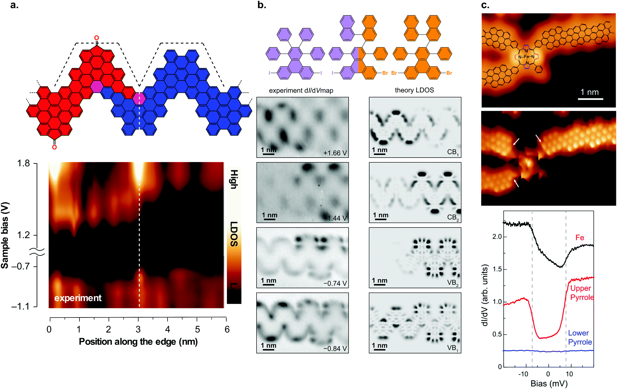 | ||
| Fig. 10 GNR heterostructures. (a) Structural model of a heterojunction between carbonyl-functionalized and pristine chevron GNRs together with dI/dV line spectra taken across the junction area. The formation of a type II heterojunction can be inferred from the dI/dV spectra. Reproduced with permission from ref. 92. Copyright 2017, Springer Nature. (b) Hierarchical formation of GNR heterojunctions through the use of a linker molecule. Below the structural model, the dI/dV maps on the junction area are shown together with the calculated LDOS. The dI/dV maps reveal that the frontier states are confined to one side of the junction. Adapted with permission from ref. 89. Copyright 2018, American Chemical Society. (c) Junction between three (3,1) ch-GNRs and an Fe porphyrin derivative. dI/dV spectra reveal that the spin state of the Fe atom is preserved upon contact with the GNRs. Reproduced with permission from ref. 226. Copyright 2018, the Authors, published by the American Association for the Advancement of Science. Provided under a Creative Commons CC BY-NC 4.0 international license. | ||
From a fabrication point of view, technological applications of these heterojunctions are not yet in view because their formation is based on stochastic processes. It is thus possible that multiple heterojunctions may form within one ribbon. By using two types of precursor molecules with different halogen substitutions (e.g. Br and I) together with a ‘linker molecule’, which has both halogen substitutions, ribbons with preferentially a single heterojunction may be formed as the two precursor molecules can only form a junction with the help of the linker molecule (Fig. 10b).89
Although research has in the beginning focused mainly on GNR–GNR junctions, a recent trend is co-deposition of small molecules to form heterostructures.226–229 Porphyrin derivatives are promising in this respect, as their central metal atom can be selected such that they possess a spin-polarized ground state. In addition, it has been shown that this spin state survives when contacted with GNRs (Fig. 10c).226 In addition, this spin state also survived in free-standing GNR–porphyrin heterostructures in two-probe conductance measurements.233 Recently, special nanographenes were found to host spin states, either due to sublattice imbalance212 or topological frustration.234–241 Thus, it may be possible to induce metal-free magnetism in nanographene–GNR heterostructures as well.
Applications
Almost a decade before the first successful synthesis of atomically precise GNRs, their electronic properties have been already predicted to be excellent for potential usage in nanoelectronic devices.28,29,146 While the previous sections deal with the synthesis and characterization of the electronic properties of GNRs, here we discuss the strategies to implement them in GNR-based devices, in particular field-effect transistors (FETs). Other applications are also under research (such as optoelectronics,228,242,243 gas sensors244 and DNA-sequencing245), but compared to FETs they are even more in their infancy.Ambient pressure chemical vapour deposition
On the road to large-scale production of GNRs and GNR-based devices, the current need for an ultra-high vacuum (UHV) environment (pressure better than 10−7 mbar) for their synthesis is one of the roadblocks with respect to both expenses and throughput.246,247 The first step to fabrication in a more readily available environment was taken by Sakaguchi et al.,246 who synthesized 5-, 7- and 9-AGNRs in a low-pressure (ca. 1 mbar) argon atmosphere using a three-stage chemical vapor deposition (CVD) process, shown in Fig. 11a. The precursor material is evaporated from a quartz boat and passes into a two-zone furnace. In the first zone, kept at 350 °C, the precursors collide with the quartz tube and dehalogenate. The biradicals then arrive at the Au/mica growth substrate in zone 2, which is kept at 250 °C and polymerize. After 15 minutes, the temperature of zone 2 is increased to 400 °C to induce cyclodehydrogenation. The setup is kept at a pressure of 1 torr of argon. These CVD-synthesized ribbons achieved lengths of up to 24 nm with an average length of around 10 nm. It should be noted that the substrate is kept at a temperature sufficient to dehalogenate the monomers, whereas it is uncertain whether biradicals are actually formed by collision with the quartz tube.248 The process was developed further by Chen et al.247 who were able to obtain 7- and 9-AGNRs as well as cGNRs (ribbon 31) with lengths up to 35 nm at ambient pressure, using a two-stage CVD process, omitting the high-temperature zone (see Fig. 11b) and increasing the pressure to atmospheric. The introduction of a small amount of hydrogen to the argon atmosphere during the synthesis was successfully shown to prevent the oxidation of the CVD-synthesized GNRs.247 XPS and HREELS data for the CVD-synthesized ribbons are comparable to UHV-synthesized GNRs, indicating that the composition of CVD-synthesized ribbons is the same as that of UHV-synthesized GNRs. The scalability of the approach is essentially only limited by the sample and setup dimensions. Optical images and Raman maps showed high uniformity over areas of square millimetres for transferred GNR films. However, the average length of the CVD-synthesized ribbons (around 10 nm) is significantly shorter than the one obtained for UHV-synthesized ribbons of various types (between 20 and 45 nm77,249,250). A comparison of UHV- and CVD-synthesized GNR FETs shows better performance for the ones containing UHV-synthesized ribbons, likely due to the difference in length.251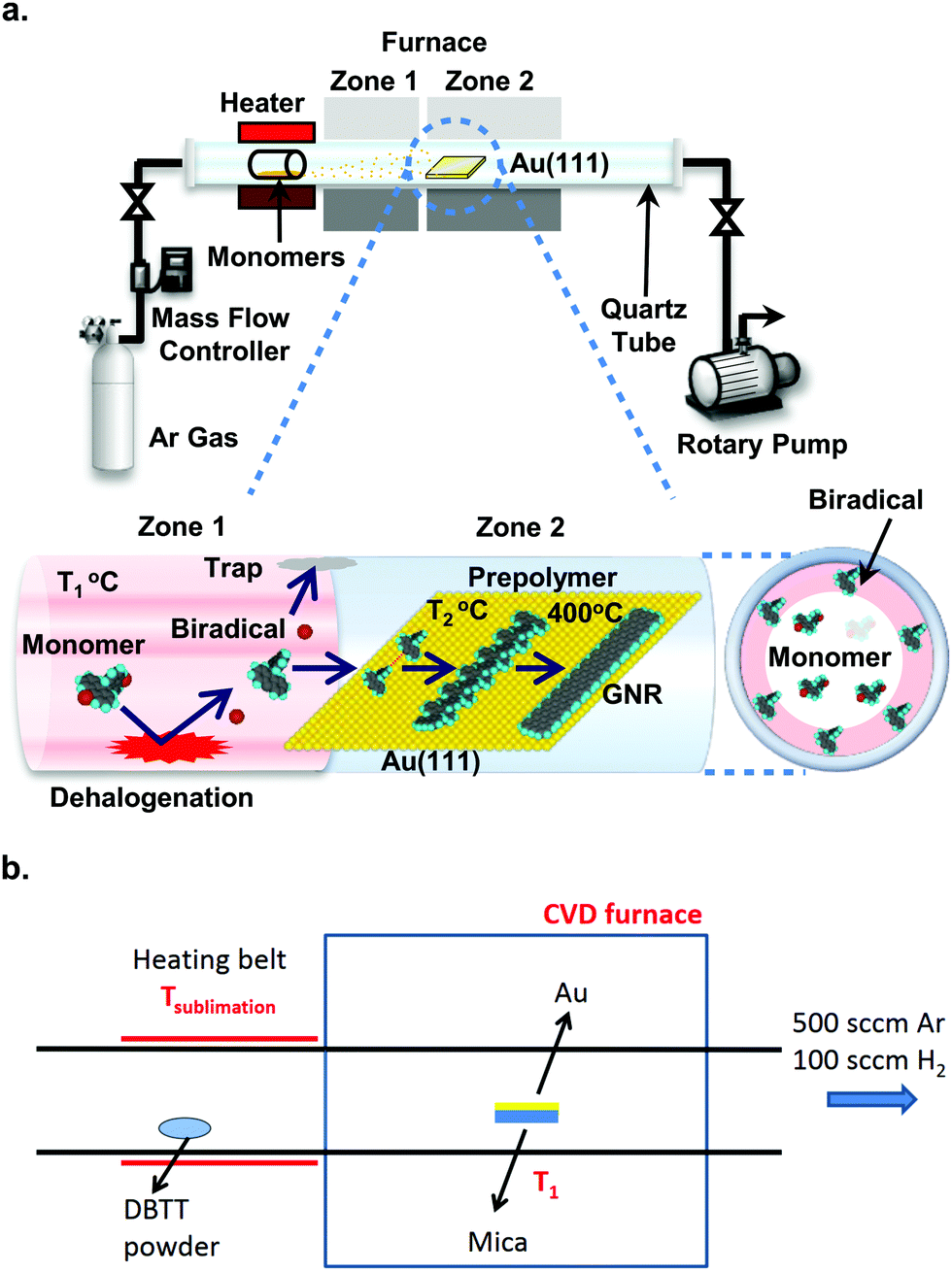 | ||
| Fig. 11 Chemical vapour deposition setups. (a) Three-stage setup developed by Sakaguchi et al. It is evacuated by a rotary pump and fed with Argon gas to a pressure of 1 torr. Stage 1: the precursor molecules are placed in a quartz boat from which they are evaporated at 250 °C. Stage 2: the precursors collide with the quartz tube wall kept at 350 °C and are dehalogenated. Stage 3: the dehalogenated precursors arrive at the Au(111)/mica substrate, which is held at 250 °C, and form polymer intermediates. These are converted to GNRs by raising the temperature of zone 2 to 400 °C. Reproduced with permission from ref. 246. Copyright 2014, Wiley-VCH. (b) Two-stage setup developed by Chen et al., which is kept at ambient pressure in a mixed argon/hydrogen atmosphere. Stage 1: the precursor is evaporated from a heating belt. Stage 2: the precursor is deposited on the Au/mica substrate, which is kept at 250 °C to form polymer intermediates. The polymers are converted to GNRs by increasing the temperature to 450 °C. Reprinted with permission from ref. 247. Copyright 2016, American Chemical Society. | ||
Besides finding ways for upscaling the fabrication conditions, the long-term stability of the ribbons under ambient conditions is also of great interest and importance. Raman spectroscopy measurements demonstrated that GNRs were stable in air up to months,252 whereas GNR FETs only showed consistent behaviour over this period in UHV and their stability under ambient conditions was limited to a handful of days.247
Aligned networks
While it is possible to fabricate single-ribbon devices, from an experimental point of view this is challenging.38,253 With a fabrication success rate of around 10% it is simply infeasible for industrial applications. Moreover, a single ribbon will also not be able to meet the performance requirements for devices (e.g. sufficient drain current for field-effect transistors79,250). Therefore, a method is sought-after to produce networks of parallel aligned GNRs, as the resistance along the ribbon is up to three orders of magnitude lower than the resistance between ribbons254 (the same principle also constitutes the main drive behind recent work to prepare aligned arrays of carbon nanotubes255,256).The synthesis of an aligned network of GNRs was first achieved by Linden et al.77 by the use of a vicinal Au(788) surface. Linden et al. demonstrated on this substrate the synthesis of aligned 7-AGNRs and chevron GNRs (31) (Fig. 12). Later studies used polarized Raman spectroscopy to show that the alignment persists over areas of up to 150 μm by 150 μm.243
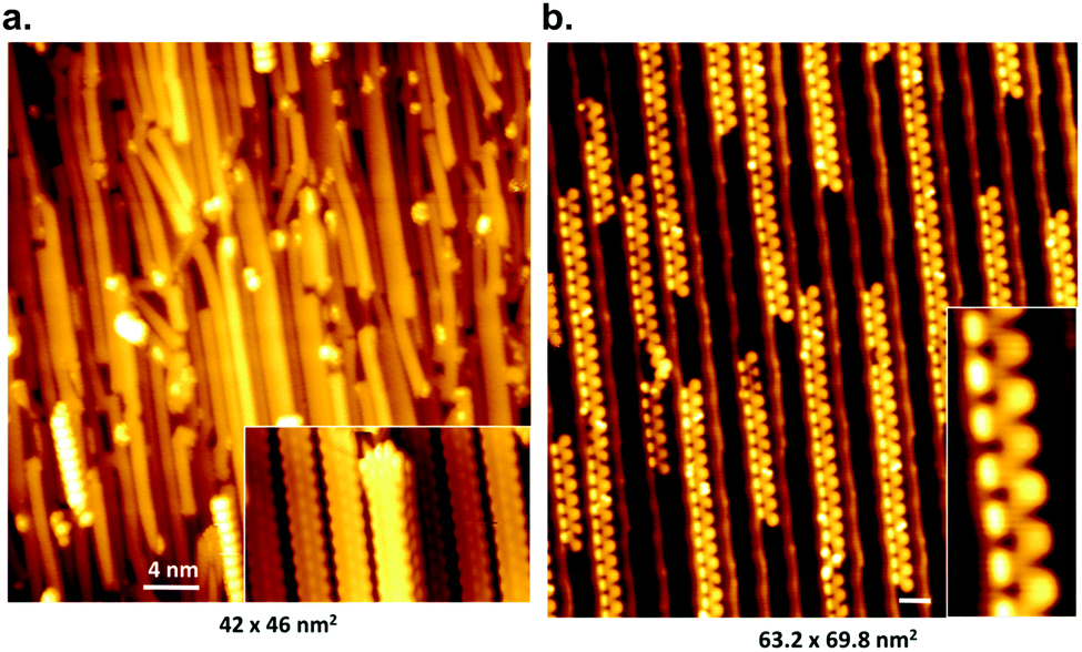 | ||
| Fig. 12 STM images of aligned graphene nanoribbons on Au(788), scale bars 4 nm. (a) 7-AGNR and (b) cGNRs (31). Reprinted figure with permission from ref. 77. Copyright 2012 by the American Physical Society. | ||
In addition to producing aligned, high-density arrays of GNRs, synthesis on a vicinal surface significantly reduces the occurrence of crosslinking defects. Lateral fusion, resulting in an array of GNRs with mixed width, is still possible but can mostly be avoided using sufficiently low temperatures during growth.79,251
Synthesis of unidirectionally aligned GNRs has also been demonstrated on the strongly anisotropic Au(110) surface, but the lower mobility on this surface results in shorter ribbons.76
Transfer methods
Regardless of the metal surface used to synthesize GNRs on, fabrication of any electronic device requires a transfer of the ribbons from the conducting metal surfaces to insulating ones, typically SiO2 on Si. Transfer by bringing the synthesis and transfer substrate into direct mechanical contact results in a transfer of some of the ribbons37 but the reproducibility of this technique is low.38 Two other methods have been developed, in particular for transfer from thin Au(111) films deposited on mica or glass. The first of these methods involves immersing the GNR/Au/mica-or-glass stack in a hydrofluoric acid solution that delaminates the GNR/Au film from its substrate. The target substrate is then used to pick up the floating GNR/Au film, and the gold is etched by a KI/I2 solution.38,246 The other common transfer method involves a poly-methyl methacrylate (PMMA) support layer, which is spin-coated onto the GNR/Au(111) sample. The mica and gold are removed as before, and then the PMMA/GNR film is brought into contact with a SiO2 substrate. This stack is heated to remove residual water and finally rinsed in acetone to remove the PMMA.38,247,253,257 The GNRs transferred this way are unfortunately distributed and oriented randomly, which hinders device fabrication as noted above.The vicinal surfaces used to synthesize aligned GNR networks are too expensive to be used only once since the etching step would dissolve them.79 However, modified versions of the support layer transfer method have been developed that preserve the Au(788) single crystal. For the first method, illustrated in Fig. 13, a hydrogen silsesquioxane (HSQ) layer is spin-coated on the GNR/Au(788) sample. The GNRs are then delaminated from the Au(788) substrate by intercalation of octanethiol (which strongly binds to noble metal surfaces258) and removed from the gold surface using a thermal release tape. This stack is placed onto the SiO2/Si substrate, the tape is removed by annealing and the HSQ layer by using a tetramethylammonium (TMAH) developer. The second method243 is based on the bubble transfer method introduced for delaminating epitaxial graphene from Cu259 and Pt260 foil. A PMMA support layer is spin-coated on the GNR/Au(788) sample and then placed in an electrochemical cell containing NaOH solution. When the gold is biased negatively, hydrogen bubbles form at the gold–GNR interface which delaminate the PMMA/GNR stack. The latter can then be transferred to the target substrate and the PMMA is removed. Both methods result in an aligned GNR film on SiO2, though polarized Raman spectroscopy shows a decrease of alignment in the GNR array after the transfer step.79,243
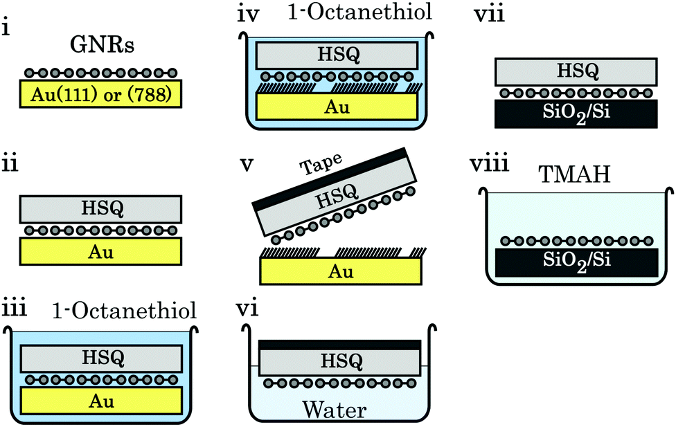 | ||
| Fig. 13 Schematic of the octanethiol-intercalation transfer method. (i) Aligned GNRs on Au(788). (ii) An HSQ support layer is spin-coated on the GNRs. (iii) The stack is submerged in an octanethiol solution. (iv) Octanethiol intercalates between GNRs and Au. (v) Thermal release tape is used to pick up the HSQ/GNR stack. (vi) Overnight immersion in water removes residual octanethiol molecules. (vii) The tape/HSQ/GNR stack is placed on SiO2/Si; the tape is removed by annealing at 120 °C. (viii) The HSQ support layer is removed by a 25% TMAH developer. Reprinted from ref. 79, with the permission of AIP Publishing. Copyright 2018, the Authors. | ||
Direct synthesis of the GNRs on insulating or semiconducting surfaces would eliminate the need for a transfer step, but challenges due to reasons highlighted above in the section on Ullmann-type coupling, have prevented this possibility until very recently.109
GNR field-effect transistor
The first studies of GNR FETs focused on the behaviour of single GNRs in an FET contacted by metal source and drain electrodes. FETs are fabricated by transfer of randomly aligned GNRs to a SiO2/Si substrate, after which metal electrodes are prepared by means of electron beam lithography and metal evaporation. Fabrication success rates for these devices were below 10% and no devices with a channel length over 30 nm (the average length of GNRs used in these studies) have so far been successfully fabricated.38 For functional devices, on/off current ratios from 103 to 105 are reported38,252,253 (approaching the typical on/off current ratios for conventional Si FETs, which range from 106 to 1010). Often the reported on/off ratio did not scale as expected with the bandgap of the different GNRs employed, although this might be explained by different experimental conditions as GNR FET characteristics are highly variable from study to study.79 On the other hand, Martini et al. compared 5- and 9-AGNR FETs and found the trend in on/off current ratio to match with the bandgaps of the ribbons.251Metal-contacted GNRs tend to be highly unstable p-type conductors in air, though might switch to n-type conduction after annealing in UHV.253 Longer channel lengths (up to 1 μm) are possible using a higher coverage of GNRs,247 but in any case device performance is limited by the Schottky-barrier contact between GNRs and metal electrodes.
Employment of graphene electrodes lowered the contact barrier, and resulted in nearly charge-neutral conducting devices regardless of environment.242,247,251 Two methods exist for preparing graphene electrodes. In the first, a graphene flake is transferred to SiO2 and a gap is opened by electroburning.251 In the second method, multilayer graphene is grown on SiC and subsequently etched into the desired shape. For both methods, the transfer of GNRs is the final step of the fabrication process. For a short channel length (up to 20 nm) and a high density of GNRs on the target substrate, a much higher reproducibility could be achieved: 30% for CVD-synthesised ribbons and up to 45% for UHV-synthesised ribbons.247,251 This difference is attributed to the difference in average length for CVD- and UHV-synthesised ribbons (there is no other difference in the structural quality of GNRs produced by each method38,247,257), as longer ribbons have a higher chance of bridging the gap between electrodes. FETs fabricated from UHV-synthesised GNRs also have a higher source–drain current. This, too, is because of the greater length of the GNRs, which leads to an increased contact area between the GNR and electrode and lowers the contact barrier.
A higher reproducibility is expected from FETs made with aligned GNR networks. Several 7-AGNR FETs79,250 have been fabricated, but the number of devices analysed is still too low to draw conclusions in a systematic way regarding the reproducibility. FETs with a channel shorter than average ribbon length show high source–drain currents while those with longer channels or ribbons aligned perpendicular to the channel show a lower source–drain current, see Fig. 14. The likely explanation for this is that the alignment of the ribbons is preserved during the device fabrication, and current is carried by GNRs spanning the channel for the first case, while in the latter two cases the resistance is dominated by ribbon–ribbon transport.
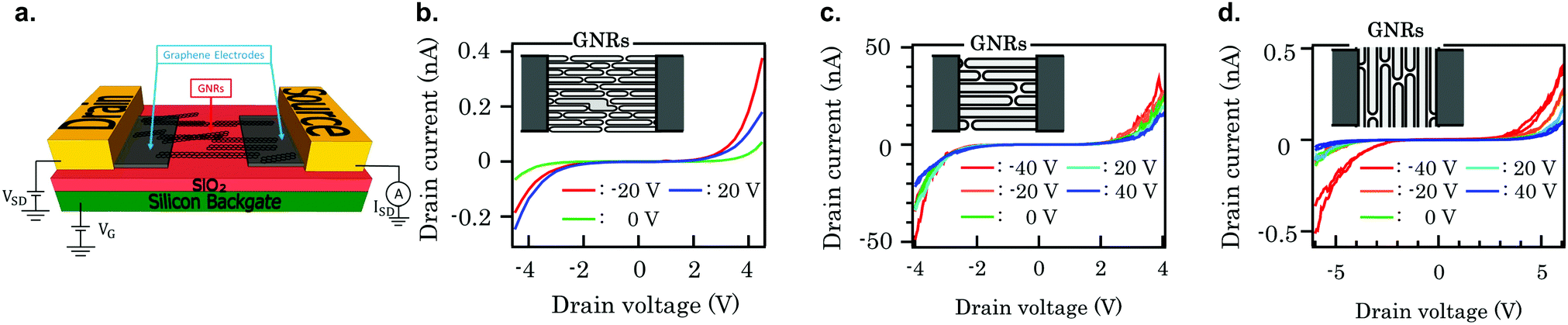 | ||
| Fig. 14 (a) Schematic of a GNR-based field effect transistor with graphene electrodes. The drain and source are metal electrodes deposited on the graphene electrodes. Reprinted from ref. 251. Copyright 2019, with permission from Elsevier. (b–d) Comparison of drain current vs drain voltage characteristics for three 7-AGNR FETs. (b) FET with a channel length L = 60 nm, width W = 50 μm, GNRs parallel to the channel. (c) FET with a channel length L = 20 nm, W = 500 nm, GNRs parallel to the channel. (d) FET with a channel length L = 20 nm, W = 500 nm, GNRs perpendicular to the channel. Reprinted from ref. 79, with the permission of AIP Publishing. Copyright 2018, the Authors. | ||
Conclusions and outlook
A decade of on-surface synthesis of GNRs has yielded a vast catalogue of synthesized and characterized GNRs, with various widths and edge structures. In this way, GNRs with varying electronic properties were synthesized, with a wide range of band gaps and in some cases even spin properties.174,261,262 The band gap of currently available GNRs ranges from approximately 0.12 to 2.4 eV,182,213 the reported effective carrier masses range from 0.02 to 0.4 me195,213 and it is very likely that newly synthesized GNRs will contribute to the extension of these ranges. The band alignment of GNRs can be effectively changed by atomically precise doping, which has only a minor impact on the band gap of the ribbons. This fine tuning of band alignment has been used to create various GNR heterojunctions, mostly based on cGNRS, in a facile manner. Since the electronic structure of GNRs is closely related to their width and edge termination, GNR heterojunctions can also be made by joining GNRs with different physical structures – something which is not possible for conventional heterostructures. GNRs offer great advantages over their parent material graphene, as they offer the possibility of having both a band gap and magnetic properties based only on their shape which is impossible for graphene. Whereas ten years ago the main focus of research was the synthesis of GNRs with various band gaps, now the field appears to be moving towards fabricating GNRs with unconventional edge structures, doping them to deliberately (fine) tune their properties and GNRs with additional phases, such as magnetic262 or topological-derived states.40–42Although much progress was made in the past ten years, some challenges remain. The predicted spin properties at the zigzag edges of ZGNRs and chGNRs could so far not be experimentally verified and, relative to the wide range of AGNRs, only a few have been synthesized. In particular, more effort should be devoted to establishing protocols for the synthesis of different ZGNRs, as only one ZGNR has been experimentally obtained thus far. Since the synthesis of these ZGNRs and chGNRs is not easily realized utilizing the most commonly employed on-surface synthesis strategy based on Ullmann-type coupling, it will be advantageous to consider other on-surface reactions, or combinations thereof. To this end, knowledge from the on-surface synthesis of 1D and 2D structures can be borrowed – a research field which has already seen a number of instructive review articles.46–48 This way GNRs which are difficult to synthesize with Ullmann-type coupling may come into reach. In addition, some of these reactions may even be suited for fabricating GNRs on semiconducting or insulating substrates or facilitate the low-temperature synthesis of GNRs. In view of getting GNRs ready for applications, these are important prerequisites.
A particularly promising route to add more functionalities to GNRs is in the form of GNR–molecule heterostructures where the molecules add properties which the GNRs do not exhibit. A few examples of such heterostructures already exist. For GNR–porphyrin junctions the spin state of the magnetic atom in the porphyrin core survived.226 In this way, magnetism can be added to GNRs. For GNR–nanographene junctions photoluminescence properties were reported.228 However, also other application possibilities are within reach. For instance, by using molecules which can undergo conformational changes mechanically moving contacts on the nanoscale are conceivable.
For moving towards device applications, it is imperative to improve ribbon length. With some notable exceptions,82,263 the typical length of on-surface synthesized GNRs is 20–45 nm, much shorter than those fabricated with other techniques, such as solution synthesis10 or lithography,8 which can produce ribbons several microns long. Since intraribbon transport is up to three orders of magnitude more efficient254 than interribbon transport this limits device performance. To increase the ribbon length, ways have to be found to stop (i) premature bonding of hydrogen to the ribbon termini and (ii) unwanted cross-linking of ribbons, for instance via ribbon alignment.
The growth of aligned bottom-up GNRs on vicinal surfaces is expected to further enhance device performance and reliability, and has prompted the development of transfer methods that do not require dissolution of the (gold) substrate used for synthesis. However, further research is needed to see whether aligned GNRs reliably perform better than unaligned ribbons grown on Au/mica samples. Nonetheless, even if performance turns out to be improved by use of aligned networks synthesized on vicinal surfaces, their increased cost might still prevent adaptation in an industrial application compared to relatively cheap Au/mica substrates.
Device fabrication requires the GNRs to be on a semiconducting or insulating surface, so for any GNR grown on a metallic substrate a transfer step is a crucial part of the device fabrication process. Further research on the transfer methods might also result in improvements of device reliability, regardless of the specific substrate used for synthesis. Inspiration might be taken from e.g. iodine intercalation to decouple covalent networks from the substrate they were synthesized on264 or the myriad methods developed to transfer transition metal dichalcogenides265–268 or graphene.269,270 Direct growth on a desired semiconductor surface, as only recently demonstrated for TiO2, is also very promising, as it completely eliminates the need for a transfer.
Synthesis outside UHV should be explored further, as UHV-synthesis is a time-consuming and expensive process. Atomically precise GNRs are expected to become more technologically appealing when their synthesis may be carried out at higher pressures. First steps have been made in this regard with ambient-pressure CVD GNR synthesis, although the length of these GNRs is even shorter than those synthesized in UHV.247 Nevertheless, CVD synthesis seems to be the way forward for GNR-based devices, as the throughput of CVD synthesis will be drastically increased compared to UHV synthesis.
In conclusion, bottom-up synthesized GNRs are a promising candidate for device applications. If the above challenges are overcome, applications of GNRs will become increasingly practical and attractive. The rapid development of bottom-up GNRs also makes the prospect of future spintronic devices increasingly likely as well.
Conflicts of interest
The authors declare no competing interests.Acknowledgements
This work was supported by the Netherlands Organization for Scientific Research (NWO) (Vici grant 680-47-633) and the Zernike Institute for Advanced Materials of the University of Groningen.Notes and references
- A. K. Geim and K. S. Novoselov, Nat. Mater., 2007, 6, 183–191 CrossRef CAS PubMed.
- D. G. Papageorgiou, I. A. Kinloch and R. J. Young, Prog. Mater. Sci., 2017, 90, 75–127 CrossRef CAS.
- A. H. Castro Neto, F. Guinea, N. M. R. Peres, K. S. Novoselov and A. K. Geim, Rev. Mod. Phys., 2009, 81, 109 CrossRef CAS.
- T. Zhang, S. Wu, R. Yang and G. Zhang, Front. Phys., 2017, 12, 127206 CrossRef.
- F. Schwierz, Nat. Nanotechnol., 2010, 5, 487 CrossRef CAS PubMed.
- K. Nakada, M. Fujita, G. Dresselhaus and M. S. Dresselhaus, Phys. Rev. B: Condens. Matter Mater. Phys., 1996, 54, 17954 CrossRef CAS PubMed.
- Z. Chen, Y. M. Lin, M. J. Rooks and P. Avouris, Phys. E, 2007, 40, 228–232 CrossRef CAS.
- M. Y. Han, B. Özyilmaz, Y. Zhang and P. Kim, Phys. Rev. Lett., 2007, 98, 206805 CrossRef PubMed.
- X. Yang, X. Dou, A. Rouhanipour, L. Zhi, H. J. Räder and K. Müllen, J. Am. Chem. Soc., 2008, 130, 4216–4217 CrossRef CAS PubMed.
- X. Li, X. Wang, L. Zhang, S. Lee and H. Dai, Science, 2008, 319, 1229–1232 CrossRef CAS PubMed.
- A. Radocea, T. Sun, T. H. Vo, A. Sinitskii, N. R. Aluru and J. W. Lyding, Nano Lett., 2017, 17, 170–178 CrossRef CAS PubMed.
- T. H. Vo, M. Shekhirev, D. A. Kunkel, M. D. Morton, E. Berglund, L. Kong, P. M. Wilson, P. A. Dowben, A. Enders and A. Sinitskii, Nat. Commun., 2014, 5, 3189 CrossRef PubMed.
- A. Narita, X. Y. Wang, X. Feng and K. Müllen, Chem. Soc. Rev., 2015, 44, 6616–6643 RSC.
- A. D. Senese and W. A. Chalifoux, Molecules, 2019, 24, 118 CrossRef PubMed.
- Y. Yano, N. Mitoma, H. Ito and K. Itami, J. Org. Chem., 2020, 85, 4–33 CrossRef CAS PubMed.
- K. Y. Yoon and G. Dong, Mater. Chem. Front., 2020, 4, 29–45 RSC.
- D. V. Kosynkin, A. L. Higginbotham, A. Sinitskii, J. R. Lomeda, A. Dimiev, B. K. Price and J. M. Tour, Nature, 2009, 458, 872–876 CrossRef CAS PubMed.
- D. V. Kosynkin, W. Lu, A. Sinitskii, G. Pera, Z. Sun and J. M. Tour, ACS Nano, 2011, 5, 968–974 CrossRef CAS PubMed.
- C. Tao, L. Jiao, O. V. Yazyev, Y.-C. Chen, X. Zhang, R. B. Capaz, J. M. Tour, A. Zettl, H. Dai and M. F. Crommie, Nat. Phys., 2011, 7, 616–620 Search PubMed.
- L. Jiao, X. Wang, G. Diankov, H. Wang and H. Dai, Nat. Nanotechnol., 2010, 5, 321–325 CrossRef CAS PubMed.
- M. Sprinkle, M. Ruan, Y. Hu, J. Hankinson, M. Rubio-Roy, B. Zhang, X. Wu, C. Berger and W. A. De Heer, Nat. Nanotechnol., 2010, 5, 727–731 CrossRef CAS PubMed.
- J. Hicks, A. Tejeda, A. Taleb-Ibrahimi, M. S. Nevius, F. Wang, K. Shepperd, J. Palmer, F. Bertran, P. Le Fèvre, J. Kunc, W. A. De Heer, C. Berger and E. H. Conrad, Nat. Phys., 2013, 9, 49–54 Search PubMed.
- M. S. Nevius, F. Wang, C. Mathieu, N. Barrett, A. Sala, T. O. Menteş, A. Locatelli and E. H. Conrad, Nano Lett., 2014, 14, 6080–6086 CrossRef CAS PubMed.
- J. Baringhaus, J. Aprojanz, J. Wiegand, D. Laube, M. Halbauer, J. Hübner, M. Oestreich and C. Tegenkamp, Appl. Phys. Lett., 2015, 106, 043109 CrossRef.
- A. Stöhr, J. Baringhaus, J. Aprojanz, S. Link, C. Tegenkamp, Y. Niu, A. A. Zakharov, C. Chen, J. Avila, M. C. Asensio and U. Starke, Ann. Phys., 2017, 529, 1700052 CrossRef.
- J. Baringhaus, M. Ruan, F. Edler, A. Tejeda, M. Sicot, A. Taleb-Ibrahimi, A. P. Li, Z. Jiang, E. H. Conrad, C. Berger, C. Tegenkamp and W. A. De Heer, Nature, 2014, 506, 349–354 CrossRef CAS PubMed.
- J. Aprojanz, S. R. Power, P. Bampoulis, S. Roche, A. P. Jauho, H. J. W. Zandvliet, A. A. Zakharov and C. Tegenkamp, Nat. Commun., 2018, 9, 4426 CrossRef PubMed.
- V. Barone, O. Hod and G. E. Scuseria, Nano Lett., 2006, 6, 2748–2754 CrossRef CAS PubMed.
- Y. W. Son, M. L. Cohen and S. G. Louie, Phys. Rev. Lett., 2006, 97, 216803 CrossRef PubMed.
- Y. Yoon and J. Guo, Appl. Phys. Lett., 2007, 91, 073103 CrossRef.
- D. Querlioz, Y. Apertet, A. Valentin, K. Huet, A. Bournel, S. Galdin-Retailleau and P. Dollfus, Appl. Phys. Lett., 2008, 92, 042108 CrossRef.
- D. Gunlycke, D. A. Areshkin and C. T. White, Appl. Phys. Lett., 2007, 90, 142104 CrossRef.
- L. Talirz, P. Ruffieux and R. Fasel, Adv. Mater., 2016, 28, 6222–6231 CrossRef CAS PubMed.
- X. Zhou and G. Yu, Adv. Mater., 2020, 32, 1905957 CrossRef CAS PubMed.
- M. Corso, E. Carbonell-Sanromà and D. G. De Oteyza, in On-Surface Synthesis II, ed. D. G. De Oteyza and C. Rogero, Springer, Cham, 2016, pp. 113–152 Search PubMed.
- Z. Chen, A. Narita and K. Müllen, Adv. Mater., 2020, 32, 2001893 CrossRef CAS PubMed.
- J. Cai, P. Ruffieux, R. Jaafar, M. Bieri, T. Braun, S. Blankenburg, M. Muoth, A. P. Seitsonen, M. Saleh, X. Feng, K. Müllen and R. Fasel, Nature, 2010, 466, 470–473 CrossRef CAS PubMed.
- J. P. Llinas, A. Fairbrother, G. Borin Barin, W. Shi, K. Lee, S. Wu, B. Yong Choi, R. Braganza, J. Lear, N. Kau, W. Choi, C. Chen, Z. Pedramrazi, T. Dumslaff, A. Narita, X. Feng, K. Müllen, F. Fischer, A. Zettl, P. Ruffieux, E. Yablonovitch, M. Crommie, R. Fasel and J. Bokor, Nat. Commun., 2017, 8, 633 CrossRef PubMed.
- C. Bronner, S. Stremlau, M. Gille, F. Brauße, A. Haase, S. Hecht and P. Tegeder, Angew. Chem., Int. Ed., 2013, 52, 4422–4425 CrossRef CAS PubMed.
- D. J. Rizzo, G. Veber, T. Cao, C. Bronner, T. Chen, F. Zhao, H. Rodriguez, S. G. Louie, M. F. Crommie and F. R. Fischer, Nature, 2018, 560, 204–208 CrossRef CAS PubMed.
- D. J. Rizzo, G. Veber, J. Jiang, R. McCurdy, T. Cao, C. Bronner, T. Chen, S. G. Louie, F. R. Fischer and M. F. Crommie, Science, 2020, 369, 1597–1603 CrossRef CAS PubMed.
- O. Gröning, S. Wang, X. Yao, C. A. Pignedoli, G. Borin Barin, C. Daniels, A. Cupo, V. Meunier, X. Feng, A. Narita, K. Müllen, P. Ruffieux and R. Fasel, Nature, 2018, 560, 209–213 CrossRef PubMed.
- E. Costa Girão, L. Liang, E. Cruz-Silva, A. G. S. Filho and V. Meunier, Phys. Rev. Lett., 2011, 107, 135501 CrossRef PubMed.
- F. Ullmann and J. Bielecki, Chem. Ber., 1901, 34, 2174–2185 CrossRef CAS.
- L. Grill, M. Dyer, L. Lafferentz, M. Persson, M. V. Peters and S. Hecht, Nat. Nanotechnol., 2007, 2, 687 CrossRef CAS PubMed.
- P. A. Held, H. Fuchs and A. Studer, Chem. – Eur. J., 2017, 23, 5874–5892 CrossRef CAS PubMed.
- L. Grill and S. Hecht, Nat. Chem., 2020, 12, 115–130 CrossRef CAS PubMed.
- S. Clair and D. G. De Oteyza, Chem. Rev., 2019, 119, 4717–4776 CrossRef CAS PubMed.
- M. Lackinger, Chem. Commun., 2017, 53, 7872–7885 RSC.
- A. Batra, D. Cvetko, G. Kladnik, O. Adak, C. Cardoso, A. Ferretti, D. Prezzi, E. Molinari, A. Morgante and L. Venkataraman, Chem. Sci., 2014, 5, 4419–4423 RSC.
- J. Björk, J. Phys.: Condens. Matter, 2016, 28, 083002 CrossRef PubMed.
- J. Björk, F. Hanke and S. Stafström, J. Am. Chem. Soc., 2013, 135, 5768–5775 CrossRef PubMed.
- M. T. Nguyen, C. A. Pignedoli and D. Passerone, Phys. Chem. Chem. Phys., 2011, 13, 154–160 RSC.
- R. Dorel and A. M. Echavarren, Eur. J. Org. Chem., 2017, 14–24 CrossRef CAS PubMed.
- F. R. Fischer, in From Polyphenylenes to Nanographenes and Graphene Nanoribbons, ed. K. Müllen and X. Feng, Springer, Cham, 2017, pp. 33–65 Search PubMed.
- J. Yamaguchi, H. Hayashi, H. Jippo, A. Shiotari, M. Ohtomo, M. Sakakura, N. Hieda, N. Aratani, M. Ohfuchi, Y. Sugimoto, H. Yamada and S. Sato, Commun. Mater., 2020, 1, 36 CrossRef.
- L. Talirz, H. Söde, T. Dumslaff, S. Wang, J. R. Sanchez-Valencia, J. Liu, P. Shinde, C. A. Pignedoli, L. Liang, V. Meunier, N. C. Plumb, M. Shi, X. Feng, A. Narita, K. Müllen, R. Fasel and P. Ruffieux, ACS Nano, 2017, 11, 1380–1388 CrossRef CAS PubMed.
- P. Ruffieux, S. Wang, B. Yang, C. Sanchez-Sanchez, J. Liu, T. Dienel, L. Talirz, P. Shinde, C. A. Pignedoli, D. Passerone, T. Dumslaff, X. Feng, K. Müllen and R. Fasel, Nature, 2016, 531, 489–492 CrossRef CAS PubMed.
- T. A. Pham, B. V. Tran, M. T. Nguyen and M. Stöhr, Small, 2017, 13, 1603675 CrossRef PubMed.
- M. Bieri, M.-T. Nguyen, O. Gröning, J. Cai, M. Treier, K. Aït-Mansour, P. Ruffieux, C. A. Pignedoli, D. Passerone, M. Kastler, K. Müllen and R. Fasel, J. Am. Chem. Soc., 2010, 132, 16669–16676 CrossRef CAS PubMed.
- C. Morchutt, J. Björk, S. Krotzky, R. Gutzler and K. Kern, Chem. Commun., 2015, 51, 2440–2443 RSC.
- T. Dienel, J. Gómez-Díaz, A. P. Seitsonen, R. Widmer, M. Iannuzzi, K. Radican, H. Sachdev, K. Müllen, J. Hutter and O. Gröning, ACS Nano, 2014, 8, 6571–6579 CrossRef CAS PubMed.
- W. Zhao, L. Dong, C. Huang, Z. M. Win and N. Lin, Chem. Commun., 2016, 52, 13225–13228 RSC.
- M. Kittelmann, M. Nimmrich, R. Lindner, A. Gourdon and A. Kühnle, ACS Nano, 2013, 7, 5614–5620 CrossRef CAS PubMed.
- M. Kolmer, A. A. Ahmad Zebari, J. S. Prauzner-Bechcicki, W. Piskorz, F. Zasada, S. Godlewski, B. Such, Z. Sojka and M. Szymonski, Angew. Chem., Int. Ed., 2013, 52, 10300–10303 CrossRef CAS PubMed.
- P. Rahe, R. Lindner, M. Kittelmann, M. Nimmrich and A. Kühnle, Phys. Chem. Chem. Phys., 2012, 14, 6544–6548 RSC.
- H. Zhang, H. Lin, K. Sun, L. Chen, Y. Zagranyarski, N. Aghdassi, S. Duhm, Q. Li, D. Zhong, Y. Li, K. Müllen, H. Fuchs and L. Chi, J. Am. Chem. Soc., 2015, 137, 4022–4025 CrossRef CAS PubMed.
- K. Sun, X. Li, L. Chen, H. Zhang and L. Chi, J. Phys. Chem. C, 2020, 124, 11422–11427 CrossRef CAS.
- P. Stoltze, J. Phys.: Condens. Matter, 1994, 6, 9495–9517 CrossRef.
- P. Han, K. Akagi, F. Federici Canova, R. Shimizu, H. Oguchi, S. Shiraki, P. S. Weiss, N. Asao and T. Hitosugi, ACS Nano, 2015, 9, 12035–12044 CrossRef CAS PubMed.
- P. Han, K. Akagi, F. Federici Canova, H. Mutoh, S. Shiraki, K. Iwaya, P. S. Weiss, N. Asao and T. Hitosugi, ACS Nano, 2014, 8, 9181–9187 CrossRef CAS PubMed.
- C. Sánchez-Sánchez, T. Dienel, O. Deniz, P. Ruffieux, R. Berger, X. Feng, K. Müllen and R. Fasel, ACS Nano, 2016, 10, 8006–8011 CrossRef PubMed.
- P. H. Jacobse, M. J. J. Mangnus, S. J. M. Zevenhuizen and I. Swart, ACS Nano, 2018, 12, 7048–7056 CrossRef CAS PubMed.
- S. Peljhan and A. Kokalj, Phys. Chem. Chem. Phys., 2011, 13, 20408–20417 RSC.
- K. A. Simonov, N. A. Vinogradov, A. S. Vinogradov, A. V. Generalov, E. M. Zagrebina, G. I. Svirskiy, A. A. Cafolla, T. Carpy, J. P. Cunniffe, T. Taketsugu, A. Lyalin, N. Mårtensson and A. B. Preobrajenski, ACS Nano, 2015, 9, 8997–9011 CrossRef CAS PubMed.
- L. Massimi, O. Ourdjini, L. Lafferentz, M. Koch, L. Grill, E. Cavaliere, L. Gavioli, C. Cardoso, D. Prezzi, E. Molinari, A. Ferretti, C. Mariani and M. G. Betti, J. Phys. Chem. C, 2015, 119, 2427–2437 CrossRef CAS.
- S. Linden, D. Zhong, A. Timmer, N. Aghdassi, J. H. Franke, H. Zhang, X. Feng, K. Müllen, H. Fuchs, L. Chi and H. Zacharias, Phys. Rev. Lett., 2012, 108, 216801 CrossRef CAS PubMed.
- P. Ruffieux, J. Cai, N. C. Plumb, L. Patthey, D. Prezzi, A. Ferretti, E. Molinari, X. Feng, K. Müllen, C. A. Pignedoli and R. Fasel, ACS Nano, 2012, 6, 6930–6935 CrossRef CAS PubMed.
- M. Ohtomo, Y. Sekine, H. Hibino and H. Yamamoto, Appl. Phys. Lett., 2018, 112, 021602 CrossRef.
- N. Merino-Díez, J. Lobo-Checa, P. Nita, A. Garcia-Lekue, A. Basagni, G. Vasseur, F. Tiso, F. Sedona, P. K. Das, J. Fujii, I. Vobornik, M. Sambi, J. I. Pascual, J. E. Ortega and D. G. De Oteyza, J. Phys. Chem. Lett., 2018, 9, 2510–2517 CrossRef PubMed.
- G. Galeotti, M. Di Giovannantonio, J. Lipton-Duffin, M. Ebrahimi, S. Tebi, A. Verdini, L. Floreano, Y. Fagot-Revurat, D. F. Perepichka, F. Rosei and G. Contini, Faraday Discuss., 2017, 204, 453–469 RSC.
- M. Di Giovannantonio, O. Deniz, J. I. Urgel, R. Widmer, T. Dienel, S. Stolz, C. Sánchez-Sánchez, M. Muntwiler, T. Dumslaff, R. Berger, A. Narita, X. Feng, K. Müllen, P. Ruffieux and R. Fasel, ACS Nano, 2018, 12, 74–81 CrossRef CAS PubMed.
- J. Eichhorn, D. Nieckarz, O. Ochs, D. Samanta, M. Schmittel, P. J. Szabelski and M. Lackinger, ACS Nano, 2014, 8, 7880–7889 CrossRef CAS PubMed.
- D. Peyrot and F. Silly, ACS Nano, 2016, 10, 5490–5498 CrossRef CAS PubMed.
- C. Bronner, T. Marangoni, D. J. Rizzo, R. A. Durr, J. H. Jørgensen, F. R. Fischer and M. F. Crommie, J. Phys. Chem. C, 2017, 121, 18490–18495 CrossRef CAS.
- P. H. Jacobse, A. van den Hoogenband, M. E. Moret, R. J. M. Klein Gebbink and I. Swart, Angew. Chem., Int. Ed., 2016, 55, 13052–13055 CrossRef CAS PubMed.
- L. Lafferentz, V. Eberhardt, C. Dri, C. Africh, G. Comelli, F. Esch, S. Hecht and L. Grill, Nat. Chem., 2012, 4, 215–220 CrossRef CAS PubMed.
- S. Kawai, S. Nakatsuka, T. Hatakeyama, R. Pawlak, T. Meier, J. Tracey, E. Meyer and A. S. Foster, Sci. Adv., 2018, 4, eaar7181 CrossRef PubMed.
- C. Bronner, R. A. Durr, D. J. Rizzo, Y.-L. Lee, T. Marangoni, A. M. Kalayjian, H. Rodriguez, W. Zhao, S. G. Louie, F. R. Fischer and M. F. Crommie, ACS Nano, 2018, 12, 2193–2200 CrossRef CAS PubMed.
- P. H. Jacobse, A. Kimouche, T. Gebraad, M. M. Ervasti, J. M. Thijssen, P. Liljeroth and I. Swart, Nat. Commun., 2017, 8, 119 CrossRef CAS PubMed.
- D. J. Rizzo, M. Wu, H.-Z. Tsai, T. Marangoni, R. A. Durr, A. A. Omrani, F. Liou, C. Bronner, T. Joshi, G. D. Nguyen, G. F. Rodgers, W.-W. Choi, J. H. Jørgensen, F. R. Fischer, S. G. Louie and M. F. Crommie, Nano Lett., 2019, 19, 3221–3228 CrossRef CAS PubMed.
- G. D. Nguyen, H. Z. Tsai, A. A. Omrani, T. Marangoni, M. Wu, D. J. Rizzo, G. F. Rodgers, R. R. Cloke, R. A. Durr, Y. Sakai, F. Liou, A. S. Aikawa, J. R. Chelikowsky, S. G. Louie, F. R. Fischer and M. F. Crommie, Nat. Nanotechnol., 2017, 12, 1077 CrossRef CAS PubMed.
- S. Blankenburg, J. Cai, P. Ruffieux, R. Jaafar, D. Passerone, X. Feng, K. Müllen, R. Fasel and C. A. Pignedoli, ACS Nano, 2012, 6, 2020–2025 CrossRef CAS PubMed.
- K. Sun, O. Krejči, A. S. Foster, Y. Okuda, A. Orita and S. Kawai, J. Phys. Chem. C, 2019, 123, 17632–17638 CrossRef CAS.
- Y.-C. Chen, T. Cao, C. Chen, Z. Pedramrazi, D. Haberer, D. G. de Oteyza, F. R. Fischer, S. G. Louie and M. F. Crommie, Nat. Nanotechnol., 2015, 10, 156–160 CrossRef CAS PubMed.
- J. Cai, C. A. Pignedoli, L. Talirz, P. Ruffieux, H. Söde, L. Liang, V. Meunier, R. Berger, R. Li, X. Feng, K. Müllen and R. Fasel, Nat. Nanotechnol., 2014, 9, 896–900 CrossRef CAS PubMed.
- C. Bronner, J. Björk and P. Tegeder, J. Phys. Chem. C, 2015, 119, 486–493 CrossRef CAS.
- A. Mairena, M. Baljozovic, M. Kawecki, K. Grenader, M. Wienke, K. Martin, L. Bernard, N. Avarvari, A. Terfort, K. H. Ernst and C. Wäckerlin, Chem. Sci., 2019, 10, 2998–3004 RSC.
- M. Abyazisani, J. M. MacLeod and J. Lipton-Duffin, ACS Nano, 2019, 13, 9270–9278 CrossRef CAS PubMed.
- B. V. Tran, T. A. Pham, M. Grunst, M. Kivala and M. Stöhr, Nanoscale, 2017, 9, 18305–18310 RSC.
- R. Zuzak, A. Jančařík, A. Gourdon, M. Szymonski and S. Godlewski, ACS Nano, 2020, 14, 13316–13323 CrossRef CAS PubMed.
- K. Sun, T. Nishiuchi, K. Sahara, T. Kubo, A. S. Foster and S. Kawai, J. Phys. Chem. C, 2020, 124, 19675–19680 CrossRef CAS.
- L. Talirz, H. Söde, J. Cai, P. Ruffieux, S. Blankenburg, R. Jafaar, R. Berger, X. Feng, K. Müllen, D. Passerone, R. Fasel and C. A. Pignedoli, J. Am. Chem. Soc., 2013, 135, 2060–2063 CrossRef CAS PubMed.
- M. Treier, C. A. Pignedoli, T. Laino, R. Rieger, K. Müllen, D. Passerone and R. Fasel, Nat. Chem., 2011, 3, 61–67 CrossRef CAS.
- J. Björk, S. Stafström and F. Hanke, J. Am. Chem. Soc., 2011, 133, 14884–14887 CrossRef PubMed.
- M. Koch, Z. Li, C. Nacci, T. Kumagai, I. Franco and L. Grill, Phys. Rev. Lett., 2018, 121, 47701 CrossRef CAS PubMed.
- P. Rempala, J. Kroulík and B. T. King, J. Org. Chem., 2006, 71, 5067–5081 CrossRef CAS PubMed.
- P. Rempala, J. Kroulík and B. T. King, J. Am. Chem. Soc., 2004, 126, 15002–15003 CrossRef CAS PubMed.
- M. Kolmer, A. K. Steiner, I. Izydorczyk, W. Ko, M. Engelund, M. Szymonski, A. P. Li and K. Amsharov, Science, 2020, 369, 571–575 CrossRef CAS PubMed.
- M. Kolmer, R. Zuzak, A. K. Steiner, L. Zajac, M. Engelund, S. Godlewski, M. Szymonski and K. Amsharov, Science, 2019, 363, 57–60 CrossRef CAS.
- A. Basagni, F. Sedona, C. A. Pignedoli, M. Cattelan, L. Nicolas, M. Casarin and M. Sambi, J. Am. Chem. Soc., 2015, 137, 1802–1808 CrossRef CAS PubMed.
- N. Merino-Díez, A. Garcia-Lekue, E. Carbonell-Sanromà, J. Li, M. Corso, L. Colazzo, F. Sedona, D. Sánchez-Portal, J. I. Pascual and D. G. De Oteyza, ACS Nano, 2017, 11, 11661–11668, DOI:10.1021/acsnano.7b06765.
- H. Huang, D. Wei, J. Sun, S. L. Wong, Y. P. Feng, A. H. C. Neto and A. T. S. Wee, Sci. Rep., 2012, 2, 983 CrossRef PubMed.
- O. Deniz, C. Sánchez-Sánchez, T. Dumslaff, X. Feng, A. Narita, K. Müllen, N. Kharche, V. Meunier, R. Fasel and P. Ruffieux, Nano Lett., 2017, 17, 2197–2203 CrossRef CAS PubMed.
- S. Wang, N. Kharche, E. Costa Girão, X. Feng, K. Müllen, V. Meunier, R. Fasel and P. Ruffieux, Nano Lett., 2017, 17, 4277–4283 CrossRef CAS PubMed.
- C. Moreno, M. Vilas-Varela, B. Kretz, A. Garcia-Lekue, M. V. Costache, M. Paradinas, M. Panighel, G. Ceballos, S. O. Valenzuela, D. Peña and A. Mugarza, Science, 2018, 360, 199–203 CrossRef CAS PubMed.
- P. H. Jacobse, R. D. McCurdy, J. Jiang, D. J. Rizzo, G. Veber, P. Butler, R. Zuzak, S. G. Louie, F. R. Fischer and M. F. Crommie, J. Am. Chem. Soc., 2020, 142, 13507–13514 CrossRef CAS PubMed.
- L. Yang, C.-H. Park, Y.-W. Son, M. L. Cohen and S. G. Louie, Phys. Rev. Lett., 2007, 99, 186801 CrossRef PubMed.
- K. Wakabayashi, K. I. Sasaki, T. Nakanishi and T. Enoki, Sci. Technol. Adv. Mater., 2010, 11, 054504 CrossRef PubMed.
- M. Fujita, K. Wakabayashi, K. Nakada and K. Kusakabe, J. Phys. Soc. Jpn., 1996, 65, 1920–1923 CrossRef CAS.
- W. Huang, J. S. Wang and G. Liang, Phys. Rev. B: Condens. Matter Mater. Phys., 2011, 84, 045410 CrossRef.
- L. Liang and V. Meunier, Appl. Phys. Lett., 2013, 102, 143101 CrossRef.
- A. Lherbier, L. Liang, J. C. Charlier and V. Meunier, Carbon, 2015, 95, 833–842 CrossRef CAS.
- R. Denk, A. Lodi-Rizzini, S. Wang, M. Hohage, P. Zeppenfeld, J. Cai, R. Fasel, P. Ruffieux, R. F. J. Berger, Z. Chen, A. Narita, X. Feng, K. Müllen, R. Biagi, V. De Renzi, D. Prezzi, A. Ruini and A. Ferretti, Nanoscale, 2017, 9, 18326–18333 RSC.
- S. Wang and J. Wang, J. Phys. Chem. C, 2012, 116, 10193–10197 CrossRef CAS.
- L. Liang and V. Meunier, J. Phys. Chem. C, 2015, 119, 775–783 CrossRef CAS.
- L. Liang and V. Meunier, Phys. Rev. B: Condens. Matter Mater. Phys., 2012, 86, 195404 CrossRef.
- J. P. Joost, A. P. Jauho and M. Bonitz, Nano Lett., 2019, 19, 9045–9050 CrossRef CAS PubMed.
- T. Cao, F. Zhao and S. G. Louie, Phys. Rev. Lett., 2017, 119, 076401 CrossRef PubMed.
- D.-X. Liu, X.-F. Li, X.-H. Zhang, X. Cao, X.-J. Zhu and D. Shi, J. Phys. Chem. C, 2020, 124, 15448–15453 CrossRef CAS.
- Y. L. Lee, F. Zhao, T. Cao, J. Ihm and S. G. Louie, Nano Lett., 2018, 18, 7247–7253 CrossRef CAS PubMed.
- R. Saito, M. Fujita, G. Dresselhaus and M. S. Dresselhaus, Phys. Rev. B: Condens. Matter Mater. Phys., 1992, 46, 1804 CrossRef CAS.
- H. Lee, Y. W. Son, N. Park, S. Han and J. Yu, Phys. Rev. B: Condens. Matter Mater. Phys., 2005, 72, 174431 CrossRef.
- J. Fernández-Rossier, Phys. Rev. B: Condens. Matter Mater. Phys., 2008, 77, 075430 CrossRef.
- O. V. Yazyev, R. B. Capaz and S. G. Louie, Phys. Rev. B: Condens. Matter Mater. Phys., 2011, 84, 115406 CrossRef.
- A. R. Carvalho, J. H. Warnes and C. H. Lewenkopf, Phys. Rev. B: Condens. Matter Mater. Phys., 2014, 89, 245444 CrossRef.
- Z. Jiang and Y. Song, Phys. B, 2015, 464, 61–67 CrossRef CAS.
- M. Ezawa, Phys. Rev. B: Condens. Matter Mater. Phys., 2006, 73, 045432 CrossRef.
- M. Ezawa, Phys. Status Solidi, 2007, 4, 489–492 CrossRef CAS.
- E. Costa Girão, E. Cruz-Silva, L. Liang, A. G. S. Filho and V. Meunier, Phys. Rev. B: Condens. Matter Mater. Phys., 2012, 85, 235431 CrossRef.
- L. Liang, E. C. Girão and V. Meunier, Phys. Rev. B: Condens. Matter Mater. Phys., 2013, 88, 035420 CrossRef.
- D. Prezzi, D. Varsano, A. Ruini and E. Molinari, Phys. Rev. B: Condens. Matter Mater. Phys., 2011, 84, 041401 CrossRef.
- D. Prezzi, D. Varsano, A. Ruini, A. Marini and E. Molinari, Phys. Rev. B: Condens. Matter Mater. Phys., 2008, 77, 041404 CrossRef.
- N. Kharche and V. Meunier, J. Phys. Chem. Lett., 2016, 7, 1526–1533 CrossRef CAS PubMed.
- J. B. Neaton, M. S. Hybertsen and S. G. Louie, Phys. Rev. Lett., 2006, 97, 216405 CrossRef CAS PubMed.
- K. Wakabayashi, Phys. Rev. B: Condens. Matter Mater. Phys., 2001, 64, 125428 CrossRef.
- E. C. Girão, E. Cruz-Silva and V. Meunier, ACS Nano, 2012, 6, 6483–6491 CrossRef PubMed.
- L. Salemi, A. Lherbier and J. C. Charlier, Phys. Rev. B, 2018, 98, 214204 CrossRef CAS.
- A. Lherbier, B. Biel, Y. M. Niquet and S. Roche, Phys. Rev. Lett., 2008, 100, 036803 CrossRef PubMed.
- F. Sánchez-Ochoa, J. Zhang, Y. Du, Z. Huang, G. Canto, M. Springborg and G. H. Cocoletzi, Phys. Chem. Chem. Phys., 2019, 21, 24867–24875 RSC.
- L. L. Cui, M. Q. Long, X. J. Zhang, X. M. Li, D. Zhang and B. C. Yang, Phys. Lett. A, 2016, 380, 730–738 CrossRef CAS.
- D. A. Areshkin and B. K. Nikolić, Phys. Rev. B: Condens. Matter Mater. Phys., 2010, 81, 155450 CrossRef.
- T. B. Martins, R. H. Miwa, A. J. R. Da Silva and A. Fazzio, Phys. Rev. Lett., 2007, 98, 196803 CrossRef CAS PubMed.
- M. Pizzochero, K. Čerņevičs, G. B. Barin, S. Wang, P. Ruffieux, R. Fasel and O. V. Yazyev, 2020, arXiv:2006.15075.
- P. H. De Oliveira Neto, J. F. Teixeira, W. F. Da Cunha, R. Gargano and G. M. E. Silva, J. Phys. Chem. Lett., 2012, 3, 3039–3042 CrossRef CAS PubMed.
- M. F. C. Fobasso, C. Kenfack-Sadem, E. Baloitcha, A. J. Fotué and L. C. Fai, Eur. Phys. J. Plus, 2020, 135, 471 CrossRef CAS.
- L. A. Ribeiro, W. F. Da Cunha, A. L. De Almeida Fonseca, G. M. e Silva and S. Stafström, J. Phys. Chem. Lett., 2015, 6, 510–514 CrossRef CAS PubMed.
- W. Ferreira Da Cunha, P. H. De Oliveira Neto, A. Terai and G. M. e Silva, Phys. Rev. B, 2016, 94, 014301 CrossRef.
- G. G. Silva, L. A. Ribeiro Junior, M. L. Pereira Junior, A. L. de Almeida Fonseca, R. T. de Sousa-Júnior and G. M. e Silva, Sci. Rep., 2019, 9, 11994 CrossRef.
- M. L. Pereira Júnior, G. M. e Silva and L. A. Ribeiro Junior, J. Phys. Chem. Lett., 2020, 11, 5538–5543 CrossRef PubMed.
- M. M. Fischer, L. A. Ribeiro Junior, W. F. da Cunha, L. E. de Sousa, G. M. e Silva and P. H. de Oliveira Neto, Carbon, 2020, 158, 553–558 CrossRef CAS.
- C. Kenfack-Sadem, M. F. C. Fobasso, F. Amo-Mensah, E. Baloitcha, A. Fotué and L. C. Fai, Physica E, 2020, 122, 114154 CrossRef CAS.
- M. L. Pereira Júnior, W. F. Da Cunha, R. T. De Sousa Junior, W. F. Giozza, G. M. e Silva and L. A. Ribeiro, J. Phys. Chem. C, 2020, 124, 22392–22398 CrossRef.
- Y. Sakai and A. Terai, J. Phys. Soc. Jpn., 2019, 88, 054718 CrossRef.
- M. L. Pereira Júnior, B. G. Enders Neto, W. F. Giozza, R. T. Sousa Júnior, G. M. e Silva and L. A. Ribeiro Júnior, J. Mater. Chem. C, 2020, 8, 12100–12107 RSC.
- N. Richter, Z. Chen, A. Tries, T. Prechtl, A. Narita, K. Müllen, K. Asadi, M. Bonn and M. Kläui, Sci. Rep., 2020, 10, 1988 CrossRef CAS PubMed.
- N. J. Van Der Kaap, I. Katsouras, K. Asadi, P. W. M. Blom, L. J. A. Koster and D. M. De Leeuw, Phys. Rev. B, 2016, 93, 140206(R) CrossRef.
- K. Asadi, A. J. Kronemeijer, T. Cramer, L. Jan Anton Koster, P. W. M. Blom and D. M. De Leeuw, Nat. Commun., 2013, 4, 1710 CrossRef PubMed.
- G. Vasseur, Y. Fagot-Revurat, M. Sicot, B. Kierren, L. Moreau, D. Malterre, L. Cardenas, G. Galeotti, J. Lipton-Duffin, F. Rosei, M. Di Giovannantonio, G. Contini, P. Le Fèvre, F. Bertran, L. Liang, V. Meunier and D. F. Perepichka, Nat. Commun., 2016, 7, 10235 CrossRef CAS PubMed.
- J. A. Lipton-Duffin, O. Ivasenko, D. F. Perepichka and F. Rosei, Small, 2009, 5, 592–597 CrossRef CAS PubMed.
- N. Abdurakhmanova, N. Amsharov, S. Stepanow, M. Jansen, K. Kern and K. Amsharov, Carbon, 2014, 77, 1187–1190 CrossRef CAS.
- A. Kimouche, M. M. Ervasti, R. Drost, S. Halonen, A. Harju, P. M. Joensuu, J. Sainio and P. Liljeroth, Nat. Commun., 2015, 6, 10177 CrossRef CAS PubMed.
- A. D. Zdetsis and E. N. Economou, Carbon, 2017, 116, 422–434 CrossRef CAS.
- J. Lawrence, P. Brandimarte, A. Berdonces-Layunta, M. S. G. Mohammed, A. Grewal, C. C. Leon, D. Sánchez-Portal and D. G. De Oteyza, ACS Nano, 2020, 14, 4499–4508 CrossRef CAS PubMed.
- Y. Que, B. Liu, Y. Zhuang, C. Xu, K. Wang and X. Xiao, J. Phys. Chem. Lett., 2020, 11, 5044–5050 CrossRef CAS PubMed.
- L. Talirz, H. Söde, S. Kawai, P. Ruffieux, E. Meyer, X. Feng, K. Müllen, R. Fasel, C. A. Pignedoli and D. Passerone, ChemPhysChem, 2019, 20, 2348–2353 CrossRef CAS PubMed.
- M. C. Chong, N. Afshar-Imani, F. Scheurer, C. Cardoso, A. Ferretti, D. Prezzi and G. Schull, Nano Lett., 2018, 18, 175–181 CrossRef CAS PubMed.
- M. Koch, F. Ample, C. Joachim and L. Grill, Nat. Nanotechnol., 2012, 7, 713–717 CrossRef CAS.
- J. Van Der Lit, M. P. Boneschanscher, D. Vanmaekelbergh, M. Ijäs, A. Uppstu, M. Ervasti, A. Harju, P. Liljeroth and I. Swart, Nat. Commun., 2013, 4, 2023 CrossRef PubMed.
- S. Wang, L. Talirz, C. A. Pignedoli, X. Feng, K. Müllen, R. Fasel and P. Ruffieux, Nat. Commun., 2016, 7, 11507 CrossRef CAS PubMed.
- C. Ma, Z. Xiao, H. Zhang, L. Liang, J. Huang, W. Lu, B. G. Sumpter, K. Hong, J. Bernholc and A. P. Li, Nat. Commun., 2017, 8, 14815 CrossRef CAS PubMed.
- H. Söde, L. Talirz, O. Gröning, C. A. Pignedoli, R. Berger, X. Feng, K. Müllen, R. Fasel and P. Ruffieux, Phys. Rev. B: Condens. Matter Mater. Phys., 2015, 91, 045429 CrossRef.
- K. A. Simonov, A. V. Generalov, A. S. Vinogradov, G. I. Svirskiy, A. A. Cafolla, C. McGuinness, T. Taketsugu, A. Lyalin, N. Mårtensson and A. B. Preobrajenski, Sci. Rep., 2018, 8, 3506 CrossRef CAS PubMed.
- P. H. Jacobse, K. A. Simonov, M. J. J. Mangnus, G. I. Svirskiy, A. V. Generalov, A. S. Vinogradov, A. Sandell, N. Mårtensson, A. B. Preobrajenski and I. Swart, J. Phys. Chem. C, 2019, 123, 8892–8901 CrossRef CAS PubMed.
- G. Borin Barin, A. Fairbrother, L. Rotach, M. Bayle, M. Paillet, L. Liang, V. Meunier, R. Hauert, T. Dumslaff, A. Narita, K. Müllen, H. Sahabudeen, R. Berger, X. Feng, R. Fasel and P. Ruffieux, ACS Appl. Nano Mater., 2019, 2, 2184–2192 CrossRef CAS.
- S. Zhao, G. B. Barin, T. Cao, J. Overbeck, R. Darawish, T. Lyu, S. Drapcho, S. Wang, T. Dumslaff, A. Narita, M. Calame, K. Müllen, S. G. Louie, P. Ruffieux, R. Fasel and F. Wang, Nano Lett., 2020, 20, 1124–1130 CrossRef CAS PubMed.
- C. Bronner, F. Leyssner, S. Stremlau, M. Utecht, P. Saalfrank, T. Klamroth and P. Tegeder, Phys. Rev. B: Condens. Matter Mater. Phys., 2012, 86, 085444 CrossRef.
- C. Bronner, M. Utecht, A. Haase, P. Saalfrank, T. Klamroth and P. Tegeder, J. Chem. Phys., 2014, 140, 024701 CrossRef PubMed.
- R. Denk, M. Hohage, P. Zeppenfeld, J. Cai, C. A. Pignedoli, H. Söde, R. Fasel, X. Feng, K. Müllen, S. Wang, D. Prezzi, A. Ferretti, A. Ruini, E. Molinari and P. Ruffieux, Nat. Commun., 2014, 5, 4253 CrossRef CAS PubMed.
- J. M. Garcia-Lastra and K. S. Thygesen, Phys. Rev. Lett., 2011, 106, 187402 CrossRef CAS PubMed.
- B. V. Senkovskiy, A. V. Fedorov, D. Haberer, M. Farjam, K. A. Simonov, A. B. Preobrajenski, N. Mårtensson, N. Atodiresei, V. Caciuc, S. Blügel, A. Rosch, N. I. Verbitskiy, M. Hell, D. V. Evtushinsky, R. German, T. Marangoni, P. H. M. van Loosdrecht, F. R. Fischer and A. Grüneis, Adv. Electron. Mater., 2017, 3, 1600490 CrossRef.
- B. V. Senkovskiy, D. Haberer, D. Y. Usachov, A. V. Fedorov, N. Ehlen, M. Hell, L. Petaccia, G. Di Santo, R. A. Durr, F. R. Fischer and A. Grüneis, Phys. Status Solidi RRL, 2017, 11, 1700157 CrossRef.
- A. Bergvall and T. Löfwander, Phys. Rev. B: Condens. Matter Mater. Phys., 2013, 87, 205431 CrossRef.
- L. Bürgi, L. Petersen, H. Brune and K. Kern, Surf. Sci., 2000, 447, L157–L161 CrossRef.
- B. V. Senkovskiy, D. Y. Usachov, A. V. Fedorov, D. Haberer, N. Ehlen, F. R. Fischer and A. Grüneis, 2D Mater., 2018, 5, 035007 CrossRef.
- N. J. Tao, Nat. Nanotechnol., 2006, 1, 173–181 CrossRef CAS PubMed.
- K. Sun, P. Ji, J. Zhang, J. Wang, X. Li, X. Xu, H. Zhang and L. Chi, Small, 2019, 15, 1804526 CrossRef PubMed.
- Y.-C. Chen, D. G. de Oteyza, Z. Pedramrazi, C. Chen, F. R. Fischer and M. F. Crommie, ACS Nano, 2013, 7, 6123–6128 CrossRef CAS PubMed.
- O. Deniz, C. Sánchez-Sánchez, R. Jaafar, N. Kharche, L. Liang, V. Meunier, X. Feng, K. Müllen, R. Fasel and P. Ruffieux, Chem. Commun., 2018, 54, 1619–1622 RSC.
- R. A. Durr, D. Haberer, Y.-L. Lee, R. Blackwell, A. M. Kalayjian, T. Marangoni, J. Ihm, S. G. Louie and F. R. Fischer, J. Am. Chem. Soc., 2018, 140, 807–813 CrossRef CAS PubMed.
- J. D. Teeter, P. Zahl, M. Mehdi Pour, P. S. Costa, A. Enders and A. Sinitskii, ChemPhysChem, 2019, 20, 2281–2285 CrossRef CAS PubMed.
- M. Shekhirev, P. Zahl and A. Sinitskii, ACS Nano, 2018, 12, 8662–8669 CrossRef CAS PubMed.
- Y. Fu, H. Yang, Y. Gao, L. Huang, R. Berger, J. Liu, H. Lu, Z. Cheng, S. Du, H. J. Gao and X. Feng, Angew. Chem., Int. Ed., 2020, 59, 8873–8879 CrossRef CAS PubMed.
- A. Keerthi, C. Sánchez-Sánchez, O. Deniz, P. Ruffieux, D. Schollmeyer, X. Feng, A. Narita, R. Fasel and K. Müllen, Chem. – Asian J., 2020, 15, 3807–3811 CrossRef CAS PubMed.
- K. A. Simonov, N. A. Vinogradov, A. S. Vinogradov, A. V. Generalov, E. M. Zagrebina, N. Mårtensson, A. A. Cafolla, T. Carpy, J. P. Cunniffe and A. B. Preobrajenski, J. Phys. Chem. C, 2014, 118, 12532–12540 CrossRef CAS.
- P. Han, K. Akagi, F. Federici Canova, H. Mutoh, S. Shiraki, K. Iwaya, P. S. Weiss, N. Asao and T. Hitosugi, ACS Nano, 2015, 9, 3404–3405 CrossRef CAS PubMed.
- K. A. Simonov, N. A. Vinogradov, A. S. Vinogradov, A. V. Generalov, E. M. Zagrebina, N. Mårtensson, A. A. Cafolla, T. Carpy, J. P. Cunniffe and A. B. Preobrajenski, ACS Nano, 2015, 9, 3399–3403 CrossRef CAS PubMed.
- F. Schulz, P. H. Jacobse, F. F. Canova, J. van der Lit, D. Z. Gao, A. van den Hoogenband, P. Han, R. J. M. Klein Gebbink, M.-E. Moret, P. M. Joensuu, I. Swart and P. Liljeroth, J. Phys. Chem. C, 2017, 121, 2896–2904 CrossRef CAS.
- N. Merino-Díez, J. Li, A. Garcia-Lekue, G. Vasseur, M. Vilas-Varela, E. Carbonell-Sanromà, M. Corso, J. E. Ortega, D. Peña, J. I. Pascual and D. G. De Oteyza, J. Phys. Chem. Lett., 2018, 9, 25–30 CrossRef PubMed.
- R. Pawlak, X. Liu, S. Ninova, P. D’Astolfo, C. Drechsel, S. Sangtarash, R. Häner, S. Decurtins, H. Sadeghi, C. J. Lambert, U. Aschauer, S. X. Liu and E. Meyer, J. Am. Chem. Soc., 2020, 142, 12568–12573 CrossRef CAS PubMed.
- J. J. Palacios, J. Fernández-Rossier and L. Brey, Phys. Rev. B: Condens. Matter Mater. Phys., 2008, 77, 195428 CrossRef.
- E. H. Lieb, Phys. Rev. Lett., 1989, 62, 1201–1204 CrossRef PubMed.
- Q. Sun, O. Gröning, J. Overbeck, O. Braun, M. L. Perrin, G. Borin Barin, M. El Abbassi, K. Eimre, E. Ditler, C. Daniels, V. Meunier, C. A. Pignedoli, M. Calame, R. Fasel, P. Ruffieux, G. B. Barin, M. El Abbassi, K. Eimre, E. Ditler, C. Daniels, V. Meunier, C. A. Pignedoli, M. Calame, R. Fasel and P. Ruffieux, Adv. Mater., 2020, 32, 1906054 CrossRef CAS PubMed.
- E. Carbonell-Sanromà, J. Hieulle, M. Vilas-Varela, P. Brandimarte, M. Iraola, A. Barragán, J. Li, M. Abadia, M. Corso, D. Sánchez-Portal, D. Peña and J. I. Pascual, ACS Nano, 2017, 11, 7355–7361 CrossRef PubMed.
- G. D. Nguyen, F. M. Toma, T. Cao, Z. Pedramrazi, C. Chen, D. J. Rizzo, T. Joshi, C. Bronner, Y.-C. Chen, M. Favaro, S. G. Louie, F. R. Fischer and M. F. Crommie, J. Phys. Chem. C, 2016, 120, 2684–2687 CrossRef CAS.
- J. Li, P. Brandimarte, M. Vilas-Varela, N. Merino-Díez, C. Moreno, A. Mugarza, J. S. Mollejo, D. Sánchez-Portal, D. Garcia De Oteyza, M. Corso, A. Garcia-Lekue, D. Peña and J. I. Pascual, ACS Nano, 2020, 14, 1895–1901 CrossRef CAS PubMed.
- R. R. Cloke, T. Marangoni, G. D. Nguyen, T. Joshi, D. J. Rizzo, C. Bronner, T. Cao, S. G. Louie, M. F. Crommie and F. R. Fischer, J. Am. Chem. Soc., 2015, 137, 8872–8875 CrossRef CAS PubMed.
- Z. Pedramrazi, C. Chen, F. Zhao, T. Cao, G. D. Nguyen, A. A. Omrani, H. Z. Tsai, R. R. Cloke, T. Marangoni, D. J. Rizzo, T. Joshi, C. Bronner, W. W. Choi, F. R. Fischer, S. G. Louie and M. F. Crommie, Nano Lett., 2018, 18, 3550–3556 CrossRef CAS PubMed.
- S. Kawai, S. Saito, S. Osumi, S. Yamaguchi, A. S. Foster, P. Spijker and E. Meyer, Nat. Commun., 2015, 6, 8098 CrossRef CAS PubMed.
- E. Carbonell-Sanromà, P. Brandimarte, R. Balog, M. Corso, S. Kawai, A. Garcia-Lekue, S. Saito, S. Yamaguchi, E. Meyer, D. Sánchez-Portal and J. I. Pascual, Nano Lett., 2020, 17, 50–56 CrossRef PubMed.
- N. Friedrich, P. Brandimarte, J. Li, S. Saito, S. Yamaguchi, I. Pozo, D. Peña, T. Frederiksen, A. Garcia-Lekue, D. Sánchez-Portal and J. I. Pascual, Phys. Rev. Lett., 2020, 125, 146801 CrossRef CAS PubMed.
- P. S. Costa, J. D. Teeter, A. Enders and A. Sinitskii, Carbon, 2018, 134, 310–315 CrossRef CAS.
- C. Ma, L. Liang, Z. Xiao, A. A. Puretzky, K. Hong, W. Lu, V. Meunier, J. Bernholc and A. P. Li, Nano Lett., 2017, 17, 6241–6247 CrossRef CAS PubMed.
- C. Ma, Z. Xiao, J. Huang, L. Liang, W. Lu, K. Hong, B. G. Sumpter, J. Bernholc and A. P. Li, Phys. Rev. Mater., 2019, 3, 016001 CrossRef CAS.
- T. Marangoni, D. Haberer, D. J. Rizzo, R. R. Cloke and F. R. Fischer, Chem. – Eur. J., 2016, 22, 13037–13040 CrossRef CAS PubMed.
- J. Li, N. M. Díez, E. C. Sanromà, M. Vilas-Varela, D. G. De Oteyza, D. Peña, M. Corso and J. I. Pascual, Sci. Adv., 2018, 4, eaaq0582 CrossRef PubMed.
- L. M. Mateo, Q. Sun, S. X. Liu, J. J. Bergkamp, K. Eimre, C. A. Pignedoli, P. Ruffieux, S. Decurtins, G. Bottari, R. Fasel and T. Torres, Angew. Chem., Int. Ed., 2020, 59, 1334–1339 CrossRef CAS PubMed.
- C. Ma, Z. Xiao, A. A. Puretzky, H. Wang, A. Mohsin, J. Huang, L. Liang, Y. Luo, B. J. Lawrie, G. Gu, W. Lu, K. Hong, J. Bernholc and A.-P. P. Li, ACS Nano, 2020, 14, 5090–5098 CrossRef CAS PubMed.
- X. Su, Z. Xue, G. Li and P. Yu, Nano Lett., 2018, 18, 5744–5751 CrossRef CAS PubMed.
- T. H. Vo, U. G. E. Perera, M. Shekhirev, M. Mehdi Pour, D. A. Kunkel, H. Lu, A. Gruverman, E. Sutter, M. Cotlet, D. Nykypanchuk, P. Zahl, A. Enders, A. Sinitskii and P. Sutter, Nano Lett., 2015, 15, 5770–5777 CrossRef CAS PubMed.
- Y. F. Zhang, Y. Zhang, G. Li, J. Lu, Y. Que, H. Chen, R. Berger, X. Feng, K. Müllen, X. Lin, Y. Y. Zhang, S. Du, S. T. Pantelides and H. J. Gao, Nano Res., 2017, 10, 3377–3384 CrossRef CAS.
- D. Beyer, S. Wang, C. A. Pignedoli, J. Melidonie, B. Yuan, C. Li, J. Wilhelm, P. Ruffieux, R. Berger, K. Müllen, R. Fasel and X. Feng, J. Am. Chem. Soc., 2019, 141, 2843–2846 CrossRef CAS PubMed.
- J. Li, N. Friedrich, N. Merino, D. G. de Oteyza, D. Peña, D. Jacob and J. I. Pascual, Nano Lett., 2019, 19, 3288–3294 CrossRef CAS PubMed.
- N. Pavliček, A. Mistry, Z. Majzik, N. Moll, G. Meyer, D. J. Fox, L. Gross, J. Su, M. Telychko, P. Hu, G. Macam, P. Mutombo, H. Zhang, Y. Bao, F. Cheng, Z. Huang and Z. Qiu, Sci. Adv., 2017, 12, eaav7717 Search PubMed.
- N. Pavliček, A. Mistry, Z. Majzik, N. Moll, G. Meyer, D. J. Fox and L. Gross, Nat. Nanotechnol., 2017, 12, 308–311 CrossRef PubMed.
- S. Mishra, X. Yao, Q. Chen, K. Eimre, O. Gröning, R. Ortiz, M. Di Giovannantonio, J. C. Sancho-García, J. Fernández-Rossier, C. A. Pignedoli, K. Müllen, P. Ruffieux, A. Narita and R. Fasel, 2020, arXiv:2003.03577.
- S. Mishra, D. Beyer, K. Eimre, J. Liu, R. Berger, O. Gro, C. A. Pignedoli, K. Mu, R. Fasel, X. Feng and P. Ruffieu, J. Am. Chem. Soc., 2019, 141, 10621–10625 CrossRef CAS PubMed.
- S. Mishra, D. Beyer, R. Berger, J. Liu, O. Gröning, J. I. J. I. Urgel, K. Müllen, P. Ruffieux, X. Feng and R. Fasel, J. Am. Chem. Soc., 2020, 142, 1147–1152 CrossRef CAS PubMed.
- S. Mishra, D. Beyer, K. Eimre, S. Kezilebieke, R. Berger, O. Gröning, C. A. Pignedoli, K. Müllen, P. Liljeroth, P. Ruffieux, X. Feng and R. Fasel, Nat. Nanotechnol., 2020, 15, 22–28 CrossRef CAS PubMed.
- S. Mishra, D. Beyer, K. Eimre, R. Ortiz, J. Fernández-Rossier, R. Berger, O. Gröning, C. A. Pignedoli, R. Fasel, X. Feng and P. Ruffieux, Angew. Chem., Int. Ed., 2020, 59, 12041–12047 CrossRef CAS PubMed.
- J. Li, S. Sanz, J. Castro-esteban, M. Vilas-varela, N. Friedrich, T. Frederiksen, D. Peña and J. I. Pascual, Phys. Rev. Lett., 2020, 124, 177201 CrossRef CAS PubMed.
- A. Candini, L. Martini, Z. Chen, N. Mishra, D. Convertino, C. Coletti, A. Narita, X. Feng, K. Müllen and M. Affronte, J. Phys. Chem. C, 2017, 121, 10620–10625 CrossRef CAS.
- B. V. Senkovskiy, M. Pfeiffer, S. K. Alavi, A. Bliesener, J. Zhu, S. Michel, A. V. Fedorov, R. German, D. Hertel, D. Haberer, L. Petaccia, F. R. Fischer, K. Meerholz, P. H. M. Van Loosdrecht, K. Lindfors and A. Grüneis, Nano Lett., 2017, 17, 4029–4037 CrossRef CAS PubMed.
- M. Mehdi Pour, A. Lashkov, A. Radocea, X. Liu, T. Sun, A. Lipatov, R. A. Korlacki, M. Shekhirev, N. R. Aluru, J. W. Lyding, V. Sysoev and A. Sinitskii, Nat. Commun., 2017, 8, 820 CrossRef PubMed.
- S. J. Heerema and C. Dekker, Nat. Nanotechnol., 2016, 11, 127–136 CrossRef CAS PubMed.
- H. Sakaguchi, Y. Kawagoe, Y. Hirano, T. Iruka, M. Yano and T. Nakae, Adv. Mater., 2014, 26, 4134–4138 CrossRef CAS PubMed.
- Z. Chen, W. Zhang, C. A. Palma, A. Lodi Rizzini, B. Liu, A. Abbas, N. Richter, L. Martini, X. Y. Wang, N. Cavani, H. Lu, N. Mishra, C. Coletti, R. Berger, F. Klappenberger, M. Kläui, A. Candini, M. Affronte, C. Zhou, V. De Renzi, U. Del Pennino, J. V. Barth, H. J. Räder, A. Narita, X. Feng and K. Müllen, J. Am. Chem. Soc., 2016, 138, 15488–15496 CrossRef CAS PubMed.
- G. Galeotti, M. Fritton and M. Lackinger, Angew. Chem., Int. Ed., 2020, 59, 22785–22789 CrossRef CAS.
- X. Y. Wang, J. I. Urgel, G. B. Barin, K. Eimre, M. Di Giovannantonio, A. Milani, M. Tommasini, C. A. Pignedoli, P. Ruffieux, X. Feng, R. Fasel, K. Müllen and A. Narita, J. Am. Chem. Soc., 2018, 140, 9104–9107 CrossRef CAS PubMed.
- V. Passi, A. Gahoi, B. V. Senkovskiy, D. Haberer, F. R. Fischer, A. Grüneis and M. C. Lemme, ACS Appl. Mater. Interfaces, 2018, 10, 9900–9903 CrossRef CAS.
- L. Martini, Z. Chen, N. Mishra, G. B. Barin, P. Fantuzzi, P. Ruffieux, R. Fasel, X. Feng, A. Narita, C. Coletti, K. Müllen and A. Candini, Carbon, 2019, 146, 36–43 CrossRef CAS.
- A. Fairbrother, J. R. Sanchez-Valencia, B. Lauber, I. Shorubalko, P. Ruffieux, T. Hintermann and R. Fasel, Nanoscale, 2017, 9, 2785–2792 RSC.
- P. B. Bennett, Z. Pedramrazi, A. Madani, Y. C. Chen, D. G. De Oteyza, C. Chen, F. R. Fischer, M. F. Crommie and J. Bokor, Appl. Phys. Lett., 2013, 103, 253114 CrossRef.
- P. Prins, F. C. Grozema, J. M. Schins, S. Patil, U. Scherf and L. D. A. Siebbeles, Phys. Rev. Lett., 2006, 96, 146601 CrossRef CAS PubMed.
- W. Sun, J. Shen, Z. Zhao, N. Arellano, C. Rettner, J. Tang, T. Cao, Z. Zhou, T. Ta, J. K. Streit, J. A. Fagan, T. Schaus, M. Zheng, S.-J. Han, W. M. Shih, H. T. Maune and P. Yin, Science, 2020, 368, 874–877 CrossRef CAS PubMed.
- L. Liu, J. Han, L. Xu, J. Zhou, C. Zhao, S. Ding, H. Shi, M. Xiao, L. Ding, Z. Ma, C. Jin, Z. Zhang and L.-M. Peng, Science, 2020, 368, 850–856 CrossRef CAS PubMed.
- Z. Chen, H. I. Wang, J. Teyssandier, K. S. Mali, T. Dumslaff, I. Ivanov, W. Zhang, P. Ruffieux, R. Fasel, H. J. Räder, D. Turchinovich, S. De Feyter, X. Feng, M. Kläui, A. Narita, M. Bonn and K. Müllen, J. Am. Chem. Soc., 2017, 139, 3635–3638 CrossRef CAS PubMed.
- C. Vericat, M. E. Vela, G. Benitez, P. Carro and R. C. Salvarezza, Chem. Soc. Rev., 2010, 39, 1805–1834 RSC.
- Y. Wang, Y. Zheng, X. Xu, E. Dubuisson, Q. Bao, J. Lu and K. P. Loh, ACS Nano, 2011, 5, 9927–9933 CrossRef CAS PubMed.
- L. Gao, W. Ren, H. Xu, L. Jin, Z. Wang, T. Ma, L.-P. Ma, Z. Zhang, Q. Fu, L.-M. Peng, X. Bao and H.-M. Cheng, Nat. Commun., 2012, 3, 699 CrossRef PubMed.
- Q. Sun, X. Yao, O. Gröning, K. Eimre, C. A. Pignedoli, K. Müllen, A. Narita, R. Fasel and P. Ruffieux, Nano Lett., 2020, 20, 6429–6436 CrossRef CAS PubMed.
- J. Li, S. Sanz, M. Corso, D. J. Choi, D. Peña, T. Frederiksen and J. I. Pascual, Nat. Commun., 2019, 10, 200 CrossRef PubMed.
- C. Moreno, M. Paradinas, M. Vilas-Varela, M. Panighel, G. Ceballos, D. Peña and A. Mugarza, Chem. Commun., 2018, 54, 9402–9405 RSC.
- A. Rastgoo-Lahrood, M. Lischka, J. Eichhorn, D. Samanta, M. Schmittel, W. M. Heckl and M. Lackinger, Nanoscale, 2017, 9, 4995–5001 RSC.
- K. K. Liu, W. Zhang, Y. H. Lee, Y. C. Lin, M. T. Chang, C. Y. Su, C. S. Chang, H. Li, Y. Shi, H. Zhang, C. S. Lai and L. J. Li, Nano Lett., 2012, 12, 1538–1544 CrossRef CAS PubMed.
- H. Jia, R. Yang, A. E. Nguyen, S. N. Alvillar, T. Empante, L. Bartels and P. X. L. Feng, Nanoscale, 2016, 8, 10677–10685 RSC.
- Z. Lin, Y. Zhao, C. Zhou, R. Zhong, X. Wang, Y. H. Tsang and Y. Chai, Sci. Rep., 2015, 5, 18596 CrossRef CAS PubMed.
- J. Xia, X. Huang, L. Z. Liu, M. Wang, L. Wang, B. Huang, D. D. Zhu, J. J. Li, C. Z. Gu and X. M. Meng, Nanoscale, 2014, 6, 8949–8955 RSC.
- M. Chen, R. C. Haddon, R. Yan and E. Bekyarova, Mater. Horiz., 2017, 4, 1054–1063 RSC.
- J. Kang, D. Shin, S. Bae and B. H. Hong, Nanoscale, 2012, 4, 5527–5537 RSC.
- Y. Zhang, Y. Zhang, G. Li, J. Lu, X. Lin, S. Du, R. Berger, X. Feng, K. Müllen and H. J. Gao, Appl. Phys. Lett., 2014, 105, 023101 CrossRef.
- D. Han, Q. Fan, J. Dai, T. Wang, J. Huang, Q. Xu, H. Ding, J. Hu, L. Feng, W. Zhang, Z. Zeng, J. M. Gottfried and J. Zhu, J. Phys. Chem. C, 2020, 124, 5248–5256 CrossRef CAS.
- D. G. De Oteyza, A. García-Lekue, M. Vilas-Varela, N. Merino-Díez, E. Carbonell-Sanromà, M. Corso, G. Vasseur, C. Rogero, E. Guitián, J. I. Pascual, J. E. Ortega, Y. Wakayama and D. Peña, ACS Nano, 2016, 10, 9000–9008 CrossRef CAS PubMed.
- L. Wang, H. Dong, Z. Guo, L. Zhang, T. Hou and Y. Li, J. Phys. Chem. C, 2016, 120, 17427–17434 CrossRef CAS.
- J. Liu, B. W. Li, Y. Z. Tan, A. Giannakopoulos, C. Sanchez-Sanchez, D. Beljonne, P. Ruffieux, R. Fasel, X. Feng and K. Müllen, J. Am. Chem. Soc., 2015, 137, 6097–6103 CrossRef CAS PubMed.
- H. Sakaguchi, S. Song, T. Kojima and T. Nakae, Nat. Chem., 2017, 9, 57–63 CrossRef CAS PubMed.
| This journal is © The Royal Society of Chemistry 2021 |