
Electronic effects of nano-confinement in functional organic and inorganic materials for optoelectronics
Jongkuk
Ko
ab,
Rüdiger
Berger
 c,
Hyemin
Lee
d,
Hyunsik
Yoon
*d,
Jinhan
Cho
*ae and
Kookheon
Char
*b
c,
Hyemin
Lee
d,
Hyunsik
Yoon
*d,
Jinhan
Cho
*ae and
Kookheon
Char
*b
aDepartment of Chemical and Biological Engineering, Korea University, 145 Anam-ro, Seongbuk-gu, Seoul 02841, Republic of Korea. E-mail: jinhan71@korea.ac.kr
bSchool of Chemical & Biological Engineering, Seoul National University, Seoul 08826, Republic of Korea. E-mail: khchar@plaza.snu.ac.kr
cPhysics at Interfaces, Max Planck Institute for Polymer Research, Ackermannweg 10, D-55128 Mainz, Germany
dDepartment of Chemical & Biomolecular Engineering, Seoul National University of Science & Technology, Seoul 01811, Republic of Korea. E-mail: hsyoon@seoultech.ac.kr
eKU-KIST Graduate School of Converging Science and Technology, Korea University, 145 Anam-ro, Seongbuk-gu, Seoul 02841, Republic of Korea
First published on 29th January 2021
Abstract
When various optically and/or electronically active materials, such as conjugated polymers, perovskites, metals, and metal oxides, are confined at the nanoscale, they can exhibit unique nano-confined behavior that significantly differs from the behavior observed at the macroscale. Although controlled nano-confinement of functional materials can allow modulation of their electronic properties without the aid of any synthetic methodologies or additional chemical treatments, limited assembly approaches for nano-confinement and insufficient analytical tools for electronic characterization remain critical challenges in the development of novel optoelectronic materials and the investigation of their modulated properties. This review describes how the nano-confined features of organic and inorganic materials are related to the control and improvement of their optoelectronic properties. In particular, we focus on various assembly approaches for effective nano-confinement as well as methods for nano-electronic characterization. Then, we briefly present challenges and perspectives on the direction of nano-confinement in terms of the preparation of optoelectronic materials with desired functionalities. Furthermore, we believe that this review can provide a basis for developing and designing next-generation optoelectronics through nano-confinement.
 Jongkuk Ko | Jongkuk Ko is a postdoctoral researcher at the Department of Chemical & Biological Engineering in Korea University in the group of Prof. Jinhan Cho. He received his PhD degree in Chemical and Biological Engineering from Seoul National University in February 2018. Under the supervision of Prof. Kookheon Char, he studied unique properties of nanoconfined conjugated polymers for optoelectronic applications. His research focuses on interfacial engineering of organic and inorganic functional materials for electronic and optoelectronic applications. |
 Rüdiger Berger | Rüdiger Berger is interested in surfaces and interface properties on the nanometer scale. He is focusing on Scanning Probe Microscopy methods. His specialty is the investigation of electrical properties of surfaces at the nanometer scale. In addition, he develops instruments for investigating drop sliding. After his physics studies in Erlangen (Germany), he developed micromechanical sensors at the IBM Research Laboratory in Rüschlikon (Switzerland). He did his doctorate in Basel (Switzerland). From 1998 to 2002 he worked at IBM Storage Systems Germany GmbH. Then he moved to the Max Planck Institute for Polymer Research in Mainz as a group leader. |
 Hyemin Lee | Hyemin Lee is a postdoctoral research fellow at Seoul National University of Science and Technology. She obtained her PhD degree from Seoul National University of Science and Technology in 2020 in the field of nanopatterning and their deformation under the supervision of Prof. Hyunsik Yoon. Her research interest is the micro/nano-patterning of various functional materials with unconventional lithography. |
 Hyunsik Yoon | Hyunsik Yoon is an associate professor in the Department of Chemical and Biomolecular Engineering at Seoul National University of Science and Technology. He obtained his PhD degree from Seoul National University in 2004 in the field of nanopatterning. After receiving his Ph. D. degree, he worked for Samsung Electronics as a senior engineer and returned to Seoul National University as a research professor. He has been a professor at Seoul National University of Science and Technology since 2012. His research interests are micro- and nanofabrication of functional materials and their applications for bio-inspired surfaces, biochips, and display/energy devices. |
 Jinhan Cho | Jinhan Cho is a professor at the Department of Chemical & Biological Engineering in Korea University since 2010. He completed MS and PhD degrees in POSTECH (1997) and Seoul National University (2001), respectively. Then, he was a postdoc at Max Planck Institute of Colloids and Interfaces (2001–2002) and University of Melbourne (2003). In 2003–2005, he was a senior researcher in LG Chemistry R&D center. In 2006–2010, he become an assistant professor in Kookmin University. His research interests are now focused on studying the surface chemistry and electrochemical properties of various organic/inorganic function materials onto textile substrates. |
 Kookheon Char | Kookheon Char is the Dean of Engineering and a Professor in the Department of Chemical and Biological Engineering at Seoul National University, Korea. He obtained his PhD degree from Stanford University in 1989 in the field of polymer physics. After the 2 year postdoctoral stint at IBM Almaden Research Center, he has served as the professor at Seoul National University since 1991. His research interests span the design, synthesis, and analysis of nano- and self-assembling materials targeting energy and IT applications. He is currently the regular member of the National Academy of Engineering of Korea. |
1. Introduction
The emergence of the Internet of Things in the era of the Fourth Industrial Revolution has greatly increased the demand for next-generation electronic devices with versatile functionality and high performance that can be embedded on curved surfaces, such as the human body. To satisfy this demand, a considerable amount of multidisciplinary research has been devoted to incorporating optoelectronic materials with a variety of functions onto soft, flexible, and curved substrates to replace conventional electronic devices based on rigid active materials with hard substrates. Particularly, the effective, robust, and selective deposition of optoelectronic materials onto soft substrates using a facile solution process as well as the synthesis of unique optoelectronic materials are key factors in the successful development of such electronic devices. That is, with the aid of spin-coating, printing, or dip-coating, a wide range of solution-processable organic and inorganic materials have been applied to various optoelectronic devices, including transistors, light emitting diodes (LEDs), photovoltaics (PVs), photodetectors, and sensors.1–7Although significant advances have been made in solution-processable optoelectronics, several unpredictable and complicated phenomena have been observed during the deposition process when changing from the solution-dispersible state to the dried/solid film state, which remain fundamental obstacles preventing complete understanding of solution-processable devices.4,8–13 Generally, solution processing of functional materials involves a series of physical operations as follows: (1) wetting of the solution on the target substrate, (2) nucleation-initiating supersaturation of the solution via solvent evaporation, (3) diffusion-induced growth of crystals, and (4) evaporation of the residual solvent. In this case, the morphological features of functional materials are sensitively influenced by slight changes in the solution conditions during the deposition process, which furthermore have a critical effect on the optoelectronic properties of the coated materials. Additionally, given that additional treatments (i.e., solution engineering, solvent annealing, and/or thermal annealing) of functional materials in the solution state (pre-treatment) and the dried state (post-treatment) can further modify the morphology of materials, various processing parameters (i.e., solvent type, deposition time, solution temperature, and annealing temperature) should also be considered during the deposition process. To our knowledge, most previous studies on controlling the nano-morphology of optoelectronic materials have mainly relied on empirical optimization because of such complicated phenomena combined with the process parameters. Thus, morphology engineering strategies using rational and predictive principles can provide a basis for developing and designing various next-generation electronics.8–13
Among the various morphology-controllable strategies, nano-confinement has substantial potential for the preparation of functional materials with desirable morphology or crystalline structures. That is, when the materials are assembled/crystallized in a nano-confined environment, their surface and interface effects in the nano-confined state operate as thermodynamically and kinetically more critical factors than those in the bulk state, which result in unusual structure behavior and functionalities. To this end, various structural confinement geometries can be used to impose different degrees of nano-confinement (i.e., 1D, 2D, and 3D), which increases the number of confining directions from one to three (Fig. 1). Specifically, thin film, cylindrical pore and spherical geometries provide ideal environments for 1D, 2D to 3D nano-confinement, respectively. For example, nano-confined polymers in thin films or cylindrical pores can exhibit morphological transformations (e.g., crystallinity, orientation and nanodomain) and dynamics that differ from those of bulk polymers, which directly affect various physical properties of the polymer, such as mechanical modulus, glass transition temperature, and viscoelastic thermodynamics.14–16 The crystallization of inorganic materials at the nanoscale can stabilize metastable phases or induce the formation of highly crystalline anisotropic structures that cannot be realized by conventional processes.17 However, despite these interesting phenomena, previous studies on nano-confinement have mainly focused on fundamental issues of structural behavior and simple physical properties rather than on device-related properties. In this regard, nano-confinement of optoelectronic materials can provide a basis for expansion to practical applications as well as comprehension of the underlying principles.
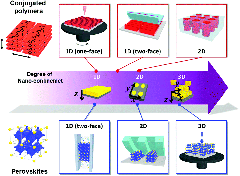 | ||
| Fig. 1 Schematic illustration of representative nano-confined assembly approaches of conjugated polymers and perovskites with different degree of nano-confinement from 1D to 3D, which increases the number of confining directions from one to three. Thin film, cylindrical pore and spherical geometries provide ideal environments for 1D, 2D to 3D nano-confinement, respectively. | ||
Conjugated polymers, as representative optoelectronic organic materials, have attracted tremendous attention due to their chemical diversity, facile processing, flexibility and chemically controllable optoelectronic properties.1–4,8,9 Additionally, solution-processable inorganic perovskites, in view of their high charge carrier mobility, long exciton diffusion length, and high absorption coefficient, have been reported to exhibit outstanding optoelectronic properties.5–7,18–20 Considerable advances in optoelectronic materials have been achieved in recent decades through material synthesis along with optimization of the processing conditions. However, as mentioned above, the complex morphological phenomena that occur during the solution process have a significant effect on the optical and electronic properties of the resultant optoelectronic material films, which are still recognized as technical difficulties. Particularly, given the intrinsic structural features of conjugated polymers with anisotropic chain molecules, the morphological features of conjugated polymers, such as the degree of crystallinity and/or chain orientation, are important factors in determining their optoelectronic properties.8,9 In the case of perovskites, engineering of rapid and strong crystallization behavior is required to produce smooth and dense perovskite films with large crystal grains.10–13 Furthermore, it is highly desirable that such films should be prepared through morphological engineering strategies based on rational and predictive principles rather than through conventional processes using empirically optimized parameters.
In line with these strategies, the effects of nano-confinement on conjugated polymers and perovskites have been intensively investigated. A few research groups have demonstrated remarkable morphological control that cannot be easily realized by conventional processes. Specifically, when poly(3-hexylthiophene-2,5-diyl) (P3HT) was infiltrated into anodized aluminum oxide (AAO) templates or imprinted with nanostructural templates, the chain orientation could be changed from edge-on to face-on or chain-on orientation, which is beneficial for out-of-plane charge transport.21–23 In addition, perovskites can form single-crystalline thin films of methylammonium lead triiodide (MAPbI3) or high-performing polymorph structures of α-phase cesium lead triiodide (CsPbI3) stabilized under ambient conditions.24–26 However, despite the effectiveness of nano-confinement, several critical issues still restrict the practical and extensive applications. That is, solution-processable optoelectronic materials have much difficulty in being incorporated into the confinement feature with the size below 100 nm. Additionally, the lack of electronic characterization tools is a critical barrier to the investigation of the structure-dependent electronic properties of optoelectronic materials at the nanoscale. Therefore, more advanced characterization tools as well as more unique assembly approaches are required for the design and development of nano-confinement-based practical applications.
In this review, we offer a comprehensive overview of the electronic effects of nano-confinement on optoelectronic materials (mainly conjugated polymers and perovskites) according to their confinement features (from 1D to 3D geometries) (Fig. 1). First, we introduce a variety of assembly approaches for nano-confinement and their characterization methods. In particular, we focus on nanoimprinting, transfer printing, and layer-by-layer (LbL) assembly, which can provide a versatile and facile way to prepare nano-confined states. Additionally, we describe the nanoscale electronic analysis of nano-confined optoelectronic materials using scanning force microscopy (SFM) in various operation modes. Furthermore, we discuss how the confinement features prepared via different assembly approaches could enhance the electronic properties and consequently improve device performance. Although a few review papers have reported nano-confinement effects on functional materials,27–29 they were mostly focused on specific aspects, such as nanoporous scaffolds to guide the crystallization and orientation of optoelectronic materials.29 Finally, we present a brief perspective on the directions of nano-confinement strategies for the realization of high-performance optoelectronic devices.
2. Solution-processable optoelectronic materials
Various types of semiconducting materials have emerged as candidates for next-generation optoelectronic devices such as photovoltaics (PVs), light emitting diodes (LEDs), photodiodes, and field effect transistors (FETs).1–7 In particular, the promise of large-area, low-cost and flexible electronics has motivated intense research on solution-processable organic or inorganic optoelectronic materials. Although solution processing of active materials has great potential as an inexpensive, facile and versatile fabrication method, solidification of materials in the solution state requires consideration of delicate physical operations, such as solution supersaturation via solvent evaporation, nucleation and crystal growth via solute movement, which significantly affect the resultant nano-morphology in an uncontrollable manner. Therefore, many methods for solution processing along with optimized deposition conditions have been suggested in accordance with the intrinsic characteristics of materials. Thus, the development of new morphological control methods, changing from empirical optimization to a predictive and controllable approach, is essential for obtaining the desired morphology and properties. Conjugated polymers and perovskites, which are among the most promising materials in this field, exhibit distinct properties of organic and inorganic materials, respectively. This review will focus on these two distinctive materials that could provide broad insight applicable to the overall field of optoelectronics. The morphological features of each material, the relationship between the nano-morphology and electronic properties and the previous approaches to control the nano-morphology will be briefly discussed in this section.2.1. Conjugated polymers
Conjugated polymers are organic macromolecules whose backbone chain is composed of alternating single and double bonds. Because of the delocalized π-electron system resulting for this chemical structure, conjugated polymers can possess various electronic and optical properties. In particular, since the electronic properties of conjugated polymers are largely determined by electron delocalization as a result of π-orbital overlap, charge transport in polymers is highly anisotropic. As shown in Fig. 2A, the charge carriers in polymers are transported along the backbone of a chain (intrachain transport) or through π–π stacking with an adjacent chain (interchain transport). Thus, the charge carrier mobility is the highest along the conjugated polymer backbone, followed by through π–π stacking structures. Therefore, macroscopic charge transport in conjugated polymers largely depends on the crystallinity, crystal size and orientation of the polymers in deposited films. In addition, different directions of charge transport in-plane (horizontal) and out-of-plane (vertical) direction with respect to the substrate should be considered when these polymers are applied to electronic devices.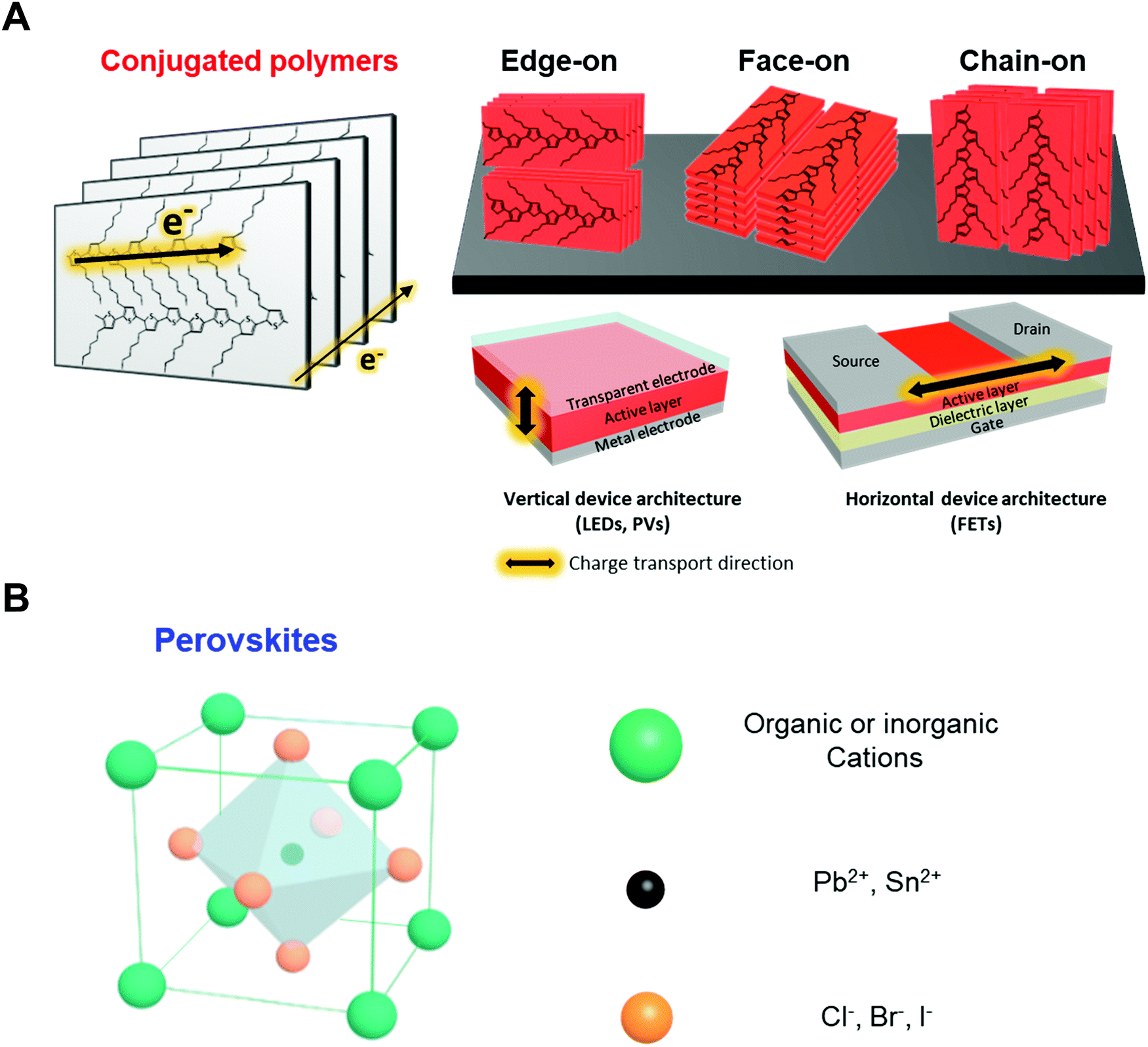 | ||
| Fig. 2 Schematic illustration of solution-processable optoelectronic materials. (A) Structural representation of conjugated polymer (P3HT) with different molecular orientations (i.e., edge-on, face-on and chain-on orientation) for different directions of charge transport and their corresponding optoelectronic applications. (B) Structural representation of perovskite, ABX3 where A is methylammonium (MA), formamidinium (FA) or Cs, B is Pb or Sn, and X is Cl, Br or I. | ||
The development of conjugated polymer devices has relied on the design and synthesis of new materials from polythiophenes to donor–acceptor conjugated copolymers. Poly(3-hexylthiophene-2,5-diyl) (P3HT)30–36 is the most widely studied conjugated polymer due to its simple chemical modification, facile processing and relatively high charge carrier mobility induced by its semicrystalline properties. Therefore, P3HT and its derivatives have been extensively employed as model polymer systems for the systematic investigation of structure–electronic property relationships. However, new types of conjugated polymers have been required due to the limited optical and electronic properties of polythiophenes (i.e., moderate level of charge mobility and limited range of optical absorption wavelengths). A new generation of conjugated polymers, donor–acceptor (D–A) conjugated copolymers, such as poly([2,6′-4,8-di(5-ethylhexylthienyl)benzo[1,2-b;3,3-b]dithiophene]{3-fluoro-2[(2-ethylhexyl)carbonyl]thieno[3,4-b]thiophenediyl}) (PTB7-th) and poly[N-9′-heptadecanyl-2,7-carbazole-alt-5,5-(4′,7′-di-2-thienyl-2′,1′,3′-benzothiadiazole)] (PCDTBT), have been synthesized and have demonstrated remarkable device performance.37–43 D–A copolymers consist of alternating electron-rich and electron-deficient units along the backbone, which leads to extensive variation in the optical and electronic properties by the appropriate choice of the donor and the acceptor units. However, these materials typically suffer from a high degree of disorder (amorphous structural properties), which has restricted their further advancement and applications, particularly for devices with vertical architectures requiring efficient out-of-plane charge transport. Approaches that can effectively control the nano-morphology of various types of conjugated polymers are highly desired.
Considering the intrinsic structural features of polymers, controlling the crystallinity and chain orientation of conjugated polymers in thin films is a crucial factor for achieving advanced electronic properties. In particular, in-plane or out-of-plane charge transport in deposited films should be considered depending on the optoelectronic device type. In contrast to transistors, which require effective charge transport along the in-plane direction, photovoltaics or photodetectors should have morphologies favorable for out-of-plane charge transport (Fig. 2A). Systematic studies are required for the rational design of assembly approaches for morphology engineering to obtain the desired functionalities.
2.2. Hybrid and all-inorganic perovskites
Perovskites usually possess the chemical composition ABX3, where X is an anion and A and B are cations of different sizes (Fig. 2B). In the case of hybrid perovskites, cation A is organic, generally methylammonium (CH3NH3+), and B is Pb2+. In all-inorganic perovskites, cation A is usually Cs+. Anion X is a halogen such as Cl−, Br−, or I−. Perovskites exhibit isotropic and highly crystalline structures that are significantly different from the structures of polymeric material. Therefore, controlling their rapid and strong crystallization during solution deposition, which has considerable effects on the optoelectronic properties, is critical. For instance, the diffusion length and mobility of charge carriers in perovskites strongly depend on the grain size of the crystals in deposited films. In particular, single crystal of MAPBI3 can exhibit diffusion lengths and charge carrier mobilities above 100 μm and 100 cm2 V−1 s−1, respectively, which are approximately two orders of magnitude higher than those of MAPBI3 in a polycrystalline state.44,45 Moreover, restricting the formation of grain boundaries, where decomposition of perovskites occurs, is critical to improve the stability of the devices.46,47 Morphology engineering has a substantial capability to enhance the performance and stability of perovskite devices.2.3. Previous approaches for controlling nano-morphology
Solution processing of optoelectronic materials requires consideration of delicate physical operations as follows: (1) wetting of the solution on the target substrate, (2) nucleation-initiating supersaturation of the solution by solvent evaporation, (3) diffusion-induced growth of crystals, and (4) evaporation of the residual solvent. A considerable amount of effort has been devoted to developing assembly approaches to optimize the nano-morphology, most of which are based on spin-coating and printing methods. Empirical optimization of the conditions of deposition methods along with additional treatments have allowed favorable nano-morphology of conjugated polymers and perovskites to be induced. However, critical challenges regarding morphology control remain, which are mainly attributed to the delicate deposition process and the requirement for complicated conditions of additional treatments of optoelectronic materials in solution states and dried states. Herein, previous approaches to morphology engineering of conjugated polymers and perovskites are briefly described for comparison to the nano-confinement based assembly approaches in the following sections.For conjugated polymers, a series of the morphological features, including the crystallinity, crystal size, and chain orientation, of deposited films must be considered due to their intrinsic molecular features. Spin-coating of conjugated polymer solutions coupled with several additional treatments has allowed good morphological control (Fig. 3A).48–54 The addition of additives,48 UV irradiation49,50 and solution aging51 have been used to induce formation of polymer crystallites in solution state. Thermal annealing53 and solvent annealing54 in the dried film state have also been shown to result in more crystalline structures. In addition to such spin-coating-based approaches, meniscus-guided deposition of polymers has recently exhibited effective morphological control based on directional assembly along with evaporation control of the solvent during deposition process.55,56 However, most of the previous approaches suffer from unpredictable morphological changes arising from the process conditions and a lack of rational design of the process steps. In particular, effective approaches to induce a morphology favorable for out-of-plane charge transport are lacking. For a more comprehensive description of the morphology engineering of conjugated polymers, the reader is referred to several recent reviews.8,9,57
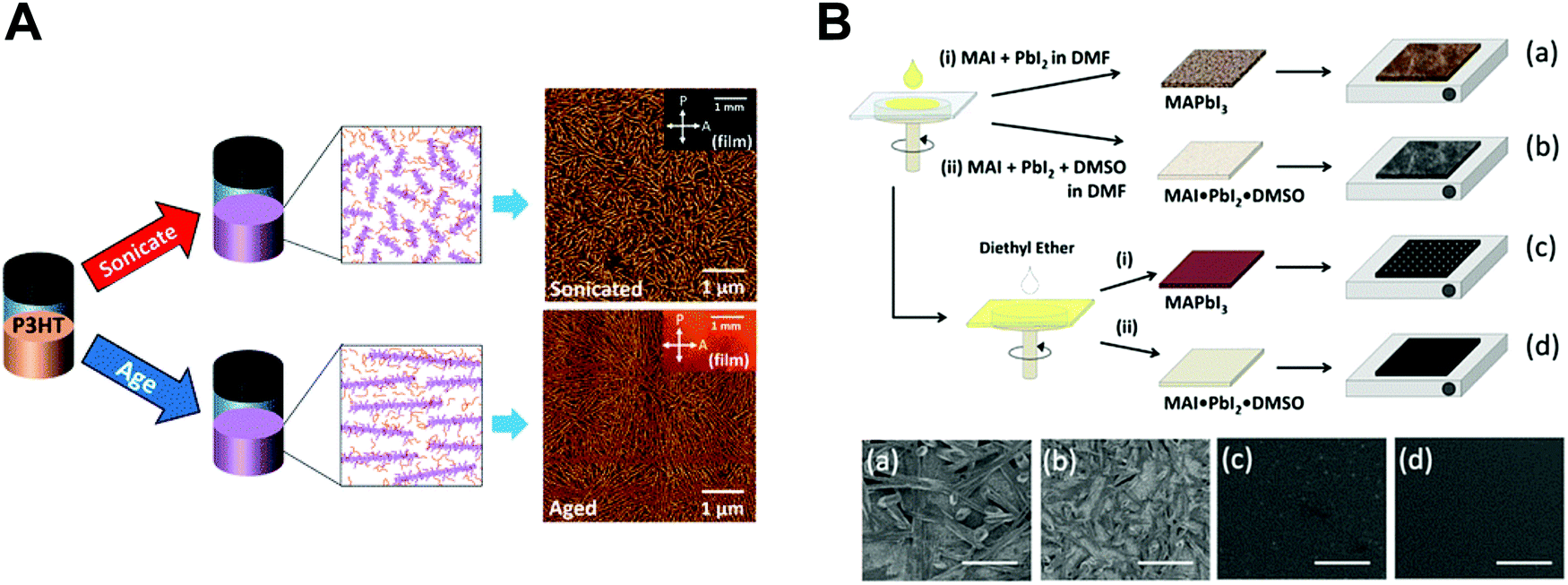 | ||
| Fig. 3 Previous approaches for controlling nano-morphology of conjugated polymers and perovskites. (A) Schematic illustration of solution engineering of conjugated polymers by ultrasonication and aging to induce crystallites and their corresponding AFM images. Adapted from ref. 51 with permission from American Chemical Society, copyright 2016. (B) Morphological changes of deposited perovskites (plane view SEM images) depending on different process conditions. Adapted from ref. 66 with permission from American Chemical Society, copyright 2015. | ||
High-quality perovskite films, which are uniform and smooth films with appropriate grain sizes, have been essential for the realization of high-performance optoelectronic devices. Rapid and uncontrollable crystallization of perovskites has made optimizing the nano-morphology of perovskites challenging.13,58–60 Thus, various morphological optimization methods such as compositional engineering,61 hot-casting,62 solvent engineering,63 and thermal/solvent annealing64,65 have been developed based on one-step66 or two-step67 deposition methods (Fig. 3B).68 The detailed development and challenges of each approach are described in previous reviews.10–13 However, most previous approaches require substantial effort to optimize the process conditions and are limited to specific process conditions for the fabrication of high-quality perovskite films. The exploration of other strategies for effective morphology engineering of optoelectronic materials must be considered.
3. Principles of nano-confinement
Nano-confined assembly/crystallization of organic and inorganic compounds has attracted multidisciplinary research interest in the areas of physics, chemistry and biology over several decades due to the large deviation in the properties from those of the bulk state.69–73 Nano-confined assembly/crystallization can have a dramatic influence on structural and physical properties depending on the confinement size and geometry. Therefore, the effects of confinement as well as subsequent structure–physical property relationships have been important subjects of previous research and reviews. These large deviations from the bulk properties are known to originate from thermodynamic and kinetic factors.16,17,29,74,75 Although the specific behavior differs according to the specific types of materials, confinement size and geometry, kinetic and thermodynamic factors enable non-equilibrium or metastable morphology/phase changes that are otherwise not achievable in a bulk process.The Gibbs free energy of the total system can be described as the sum of the volume free energy and surface free energy as follows:
| G = GV + GA |
where GV is the volume free energy, GA is the surface free energy, A is the mean total surface area, V is the mean volume, ρ is the bulk crystal density, and Gα is the average surface energy at the unit crystal surface. As the surface-to-volume ratio of confined materials increases (the confinement sizes decrease), the contribution of the surface free energy to the total Gibbs energy can be substantially increased, thus stabilizing metastable phases in the confined geometry.

A further effect of nano-confinement arising from kinetic effects is also expected. The crystallization behavior of various materials is typically determined by the nucleation and diffusion of the component materials. When crystallization occurs under nano-confinement, crystal growth is retarded due to the decreased nucleation and diffusion rates in the confined state. These effects are mainly attributed to the reduced crystallization volume, which limits the inclusion of impurities and the probability of nucleation as well as the diffusion of reacting materials. Therefore, crystallization under nano-confinement can lead to single-crystal or highly-crystalline structures of various materials. Moreover, confinement with an anisotropic geometry can result in an anisotropic crystal shape because of the faster growth along the unrestricted pore dimension.
Effective utilization and comprehensive understanding of nano-confinement effects could have potential impacts on various fields based on the ability to guide formation of desirable crystal structures and morphologies using various materials. In this section, previous studies on nano-confinement based on polymers and inorganic materials are briefly summarized.
3.1. Polymers under nano-confinement
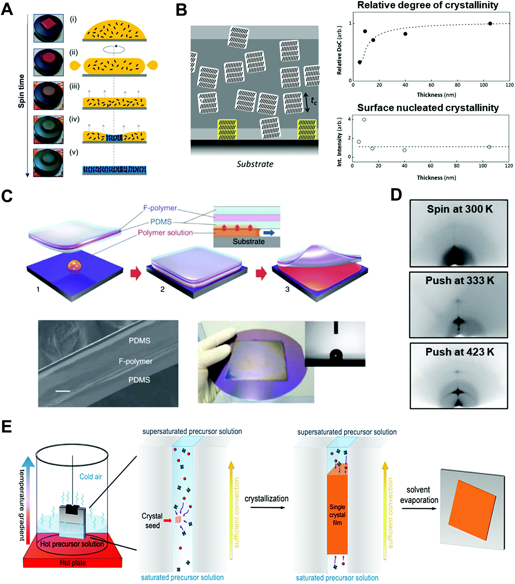
Polymers, composed of long repeating units of monomers, have a variety of conformational states (i.e., the spatial configuration of the connected monomers), which ultimately determine various properties of the polymers. In general, the processing of polymers follows a series of physical operations, such as solvent evaporation and solute movement, as well as forces exerted on the polymer chains, which alter the conformation of the polymers during the deposition process. Such complicated phenomena during the processing of polymers often result in unexpected morphological changes in the deposited states. Confinement of polymers at the nanoscale can have a dominant influence on the conformations of the macromolecular chain by spatial constraints76 and interfacial effects.77,78 Thus, the assembly of polymers under nano-confinement could be used to effectively control the conformation of polymers to achieve desired nano-morphologies and properties that have not been achievable via conventional processes.A number of previous studies on the nano-confinement effect on polymers have been conducted based on thin film states deposited on flat substrates. Spin-coating methods allow the preparation of polymeric thin films with controllable thickness for systematic studies on nano-confinement. A bilayer model (or trilayer model) has usually been used to describe the effects of nano-confinement on polymers, which consists of a bulk-like layer and an interfacial layer(s) (Fig. 4A).15,79–81 As the mobility of polymer chains is altered by confinement, nano-confinement was found to have considerable effects on the crystallization behavior of polymers, which results in unique film morphologies,15,82–84 and physical properties such as mechanical properties,85–87 glass transition temperatures,16,79,80 and melting temperatures.15,83,88 For example, the crystallization of PS/PEO layered films was significantly altered depending on the thickness of the films (confinement size) (Fig. 4B).82 The radial lamellar growth of PEO crystals in 21 μm-thick films changed into single-crystal-like lamellar structures oriented along the horizontal direction at a thickness under 100 nm. In addition, the deviation of Tg from the bulk value (Tg − Tbulkg) was highly correlated with the film thickness (confinement size), as shown in Fig. 4C.80
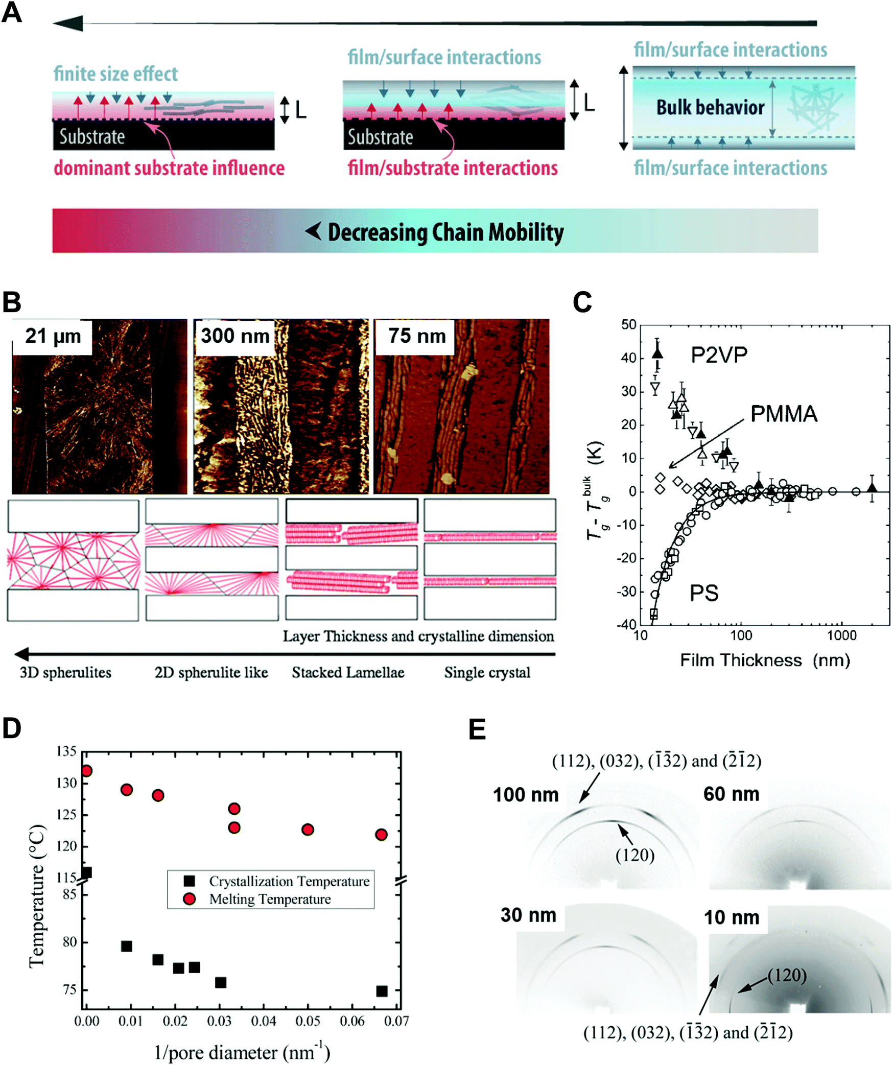 | ||
| Fig. 4 (A) Schematic illustration of bilayer model to explain nano-confinement effect on polymers. Adapted from ref. 81 with permission from American Chemical Society, copyright 2018. (B) AFM phase images of PS/PEO layered films with different thickness and schematic illustration showing morphology changes of PS/PEO films depending on film thickness. Adapted from ref. 82 with permission from American Chemical Society, copyright 2018 and from ref. 84 with permission from Material Research Science, copyright 2012. (C) Tg − Tbulkg of PS film, PMMA film and P2VP film as a function of film thickness. Adapted from ref. 80 with permission from American Chemical Society, copyright 2007. (D) Crystallization temperature and melting temperature of PE infiltrated in AAO templates as a function of the inverse of the pore diameter of AAO. Adapted from ref. 14 with permission from John Wiley and Sons, copyright 2014. (E) Wide-angle X-ray diffraction (WAXD) 2D patterns of PEO infiltrated in AAO with different pore sizes. Adapted from ref. 90 with permission from American Chemical Society, copyright 2013. | ||
More pronounced confinement can be achieved by using 2-dimensional or 3-dimensional geometries. In particular, because of a higher surface-to-volume ratio combined with a severely anisotropic geometry, 2D confinement has substantial impacts on the properties of polymers. Various types of polymers have been infiltrated into AAO templates to investigate nano-confinement effects. For example, when polymers (e.g., PE, PEO, and PS) crystallized in the nanopores of AAO, in addition to decrease in Tm (melting temperature) and Tc (crystallization temperature) (Fig. 4D),14,15,89 changes in the crystal orientation were observed depending on the sizes of the nanopores (Fig. 4E).14,15,90 The effects of nano-confinement with 3D geometries on polymers have also been investigated. For example, confined assembly of various block-copolymers in colloidal states (3D nano-confined state) showed unique morphological changes that significantly differed from those observed in thin films (1D nano-confined state) and cylindrical nanopores (2D nano-confined state).91–95 However, 3D confinement can have limited effects on the crystallization behavior of polymers and their subsequent physical properties due to the anisotropic molecular structures of polymers. Assembly of polymers under 2D nano-confinement will be highly desirable for further device-related applications, which can take advantage of the considerable anisotropy of polymers from 2D nano-confining geometries.
3.2. Inorganic compounds under nano-confinement
Inorganic materials exhibit different behavior under nano-confinement due to their rapid and strong crystallization characteristics. Thus, 2D or higher degrees of confined geometries have been widely exploited rather than 1D thin film states to offer an environment for more pronounced confinement. Several interesting phenomena have been observed depending on thermodynamic and kinetic factors. For instance, reducing the volumes for crystallization of inorganic compounds (i.e., increasing the surface-to-volume ratios) induces a surface-energy-driven phase transformation which involves crystalline structures that are metastable in the bulk state.17,96,97 In addition, retarded crystallization kinetics combined with anisotropic templates enable anisotropic single-crystalline structures or unique template-driven shapes.17,98,99 For example, the polymorph of potassium ferrocyanide (K4Fe(CN)6) was significantly affected when it was precipitated within pore glasses (CPGs) with pore diameters of 8, 48, and 362 nm. Specifically, slow transformation to the metastable tetragonal polymorph occurred, which was stable for a month in 8 nm pores.97 Moreover, calcium phosphate formed anisotropic crystals under a nanopore of membrane (Fig. 5A),98 and calcium carbonate formed crystals of unique porous shapes under a colloidal crystal template (Fig. 5B).99 These unusual crystalline structures and morphologies induced by nano-confinement have shown potential for application in various fields, such as biomineralization and synthesis of nanomaterials. However, the difficulty of removing templates from nano-confined materials seriously restricts their practical applications.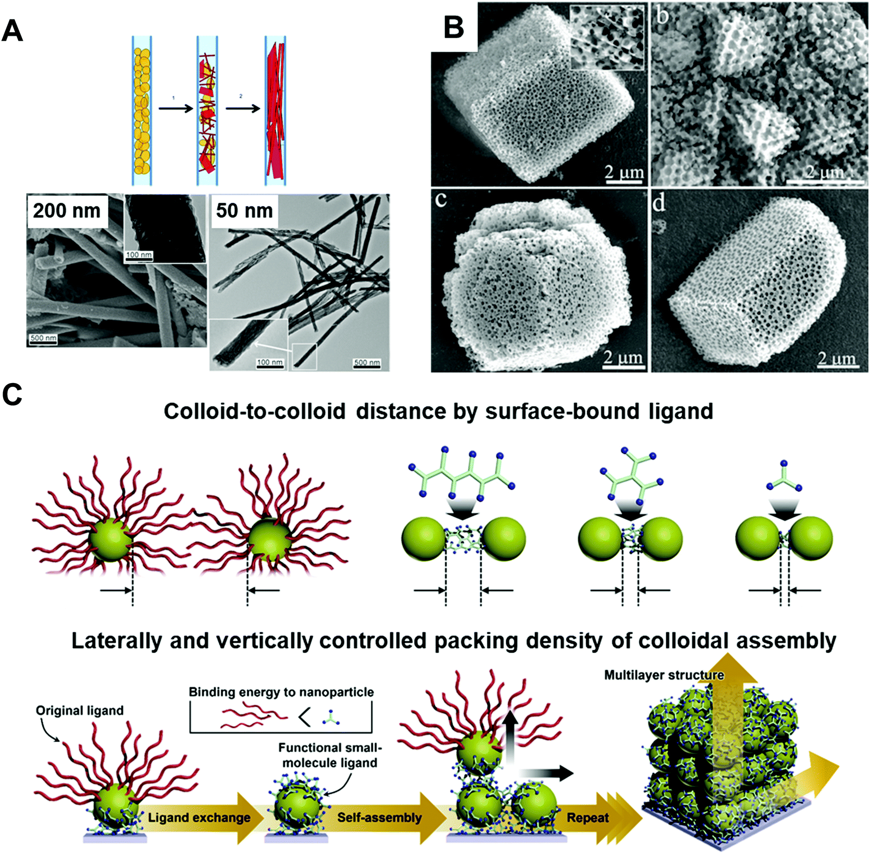 | ||
| Fig. 5 (A) Precipitation of calcium phosphate within nano-pores of the membrane with different pore-sizes showing preferential orientation along pore directions. Adapted from ref. 98 with permission from John Wiley and Sons, copyright 2013. (B) Calcium carbonate crystals precipitated in colloidal crystal template with various shapes. Adapted from ref. 99 with permission from John Wiley and Sons, copyright 2010. (C) Schematic illustration of assembled colloid composite with different structural parameters. Adapted from ref. 104 with permission from John Wiley and Sons, copyright 2020. | ||
Organic ligand-stabilized inorganic nano-colloids can provide a favorable interfacial environment for 3D nano-confinement through the type, size, and hydrophobicity/hydrophilicity of the organic ligands, and furthermore, synthetic condition-dependent size control of nano-colloids can be used to systematically investigate the relation between the nano-colloidal size and nano-confinement. Particularly, the physical properties of nano-colloids can be considerably different from those of the bulk state. For example, size-dependent phase diagrams of semiconducting nano-colloids such as quantum dots (CdSe, CdS, etc.)100,101 and a significant decrease in the melting temperature of metal nano-colloids (e.g., Au, Ag, and Pt)102,103 have been widely observed in previous studies.
In addition to nano-colloids themselves, nano-colloidal assembly to form a composite state as another 3D nano-confined system also shows unique and distinctive collective properties depending on various structural parameters, such as the colloid size, colloid-to-colloid distance, and thickness of the composite (Fig. 5C).17,104 Based on these properties, several different assembly approaches (i.e., spin-coating, drop-casting, and printing) have been applied to prepare nano-colloidal composites with collective properties. However, the abovementioned approaches suffer from the critical drawback that the composite thickness at the nanometer level, the colloid-to-colloid distance, and the interfacial interactions, which are important structural factors for 3D nano-confinement systems, cannot be precisely controlled. As an alternative, LbL assembly, particularly ligand-exchange LbL (LE-LbL) assembly based on the complementary interactions between neighboring components, has recently emerged as one of the most promising deposition approaches for 3D nano-confinement. This approach can be used to effectively fabricate nano-colloidal composites to obtain the desired physical (e.g., nanometer-level thickness, packing density, and loading amount from nanograms to micrograms per unit area) and chemical (e.g., chemical composition and hydrophobic/hydrophilic balance) properties irrespective of the substrate size and shape. More detailed explanations of this emerging technology as well as its applications using electronically and/or optically active nano-colloids will be given in the following sections.
4. Assembly approaches and electronic characterization for nano-confinement
Previous studies on nano-confinement have mainly focused on fundamental understanding of the peculiar behavior and the consequent deviation of the physical properties from those of the bulk state; thus, this approach is far from device-related practical applications. This review aims to extend the capability of nano-confinement to optoelectronic materials to modulate the electronic properties of materials to enhance device performance. Despite intense research efforts in this field, critical challenges remain that hinder further applications in optoelectronic devices, mainly stemming from the restricted assembly approaches for confinement and the lack of nanoscale electronic characterization. Previous methods, recent advances and emerging new technologies in assembly approaches and nano-characterization methods are summarized below.4.1. Assembly approaches for nano-confinement of optoelectronic materials
A high degree of confinement is desirable to obtain better morphological control of various materials. However, at the same time, this is often associated with difficulties in the assembly process. Moreover, when nano-confined materials are applied to optoelectronic devices, several other factors should also be considered, such as how to incorporate them into devices and how compatible they are with devices. Particularly, the nano-confined optoelectronic materials should be prepared on target electrodes without sacrificing their optoelectronic properties, and, furthermore, complementary interactions between vertically coated heterogeneous materials (e.g., metal electrode/optoelectronic materials or charge-transporting layer/optoelectronic material layer) should also be taken into account for the actual device applications. In this part, we describe previous assembly approaches for nano-confinement and evaluate their effectiveness based on two representative organic and inorganic optoelectronic materials: conjugated polymers and perovskites (summarized in Table 1).| Confined geometry | Assembly approach | Size range | Process condition | Material | Morphology feature | Ref. |
|---|---|---|---|---|---|---|
| a RT: room temperature. b g-Coated: graphene coated substrate. | ||||||
| 1D (one-face) | Spin-coating | 5–200 nm | RTa | P3HT | Edge-on orientation | 112 and 113 |
| Decreased crystallinity | ||||||
| Spin-coating on g-coatedb | 10–50 nm | RT | P3HT | Face-on orientation | 114 and 115 | |
| 1D (two-face) | Push coating | 10–1000 nm | 25–150 °C, 150 Pa, | P3HT | Edge-on orientation | 126 |
| Increased crystallinity | ||||||
| Soft cover | 250 nm–2 μm | 80–140 °C | MAPbI3 | Smooth surface | 129–131 | |
| Large grain size | ||||||
| Hard cover | 13 nm–200 μm | 90–100 °C | MAPbI3 | Thin single crystal | 24 and 132 | |
| 2D | Nanoimprint silicon mold (line) | 100 nm–560 μm | 150–170 °C | P3HT | Chain-on orientation | 21, 23, 141 and 142 |
| 30–50 bar | ||||||
| Nanoimprint AAO (pillar) | 150 nm | 250 °C | P3HT | Chain-on orientation | 22 | |
| Nanoimprint PDMS (pillar) | ∼6 μm | 200 °C | P3HT | Chain-on orientation | 143 | |
| Solvent-assisted nanoimprint silicon mold (line) | 50–210 nm | RT 60 bar | P3HT | Face-on orientation | 144 and 145 | |
| Solvent-assisted nanoimprint AAO (pillar) | 160 nm | RT 60 bar | P3HT | Face-on orientation | 146 | |
| Infiltration silicon mold | 200 nm | RT, solvent evaporation | P3HT/PCBM blend | Face-on orientation | 147 | |
| Transfer printing PTFE (pillar) | 30–170 nm | 40–50 °C | P3HT | Face-on orientation | 148 and 149 | |
| 4 bar | PCDTBT | |||||
| PTB-th Blends | ||||||
| Infiltration AAO (pillar) | 10–400 nm | Spin coating followed by annealing (100 °C) | MAPbI3 | − α-phase CsPbI3 | 25, 150 and 151 | |
| MAPbI3−xClx | − Uniform and well-crystallized layer | |||||
| CsPbBr3 | ||||||
| CsPbI3 | ||||||
| Infiltration AAO (pillar) | ∼40 nm | Electrochemical deposition | MAPbI3 | Single-crystal nanowire | 152 | |
| 2D | Solvent-assisted nanoimprint silicon, PUA (pillar) | 200–500 nm | 100 °C | MAPbI3 | – Smooth surface | 153–155 |
| 70–100 bar | – Improved crystallinity | |||||
| – Shrinkage of grain boundaries | ||||||
| Additive-assisted nanoimprint PDMS (line) | 200–500 nm | 80 °C | MAPbI3 | – Smooth surface | 156 and 157 | |
| <1 bar | CsPbI3 | – Improved crystallinity | ||||
| – α-Phase CsPbI3 | ||||||
| Filling by asymmetric wetting chemical line pattern | 1000 nm | 80 °C | CsPbI3 | – Improved crystallinity | 158 | |
| – α-Phase CsPbI3 | ||||||
| – Large grain size | ||||||
| Liquid phase transformation PDMS (line) | 735–1500 nm | 100 °C | MAPbI3 | – Smooth surface | 159 | |
| – Improved crystallinity | ||||||
| – Shrinkage of grain boundaries | ||||||
| 3D | Spin assisted LbL with nano-colloids | ∼100 nm per every step | Ambient conditions | CsPbI3 | Composite states with α-CsPbI3 | 26 and 185–187 |
 | ||
| Fig. 6 Thin film based 1D nano-confinement approaches for optoelectronic materials. (A) Videomicroscopy images and corresponding schematic illustration showing the spin-coating procedures. Adapted from ref. 52 with permission from American Chemical Society, copyright 2017. (B) (left) Schematic of three-layer model describing nano-confinement effect of P3HT thin films and (right) relative degree of crystallinity (DoC) and surface nucleated crystallinity of P3HT films as a function of film thickness measured by GIXD. Adapted from ref. 112 with permission from John Wiley and Sons, copyright 2013. (C) Schematic illustration of push coating of conjugated polymer films and (D) 2D X-ray diffraction images of P3HT films prepared at different processing conditions. Adapted from ref. 126 under a Creative Commons Attribution-NonCommercialShare Alike 3.0 Unported License (https://creativecommons.org/licenses/by-nc-sa/3.0/), copyright 2012 Springer Nature. (E) Schematic illustration of procedure for fabricating perovskite single-crystalline thin films by 1D-confined geometry. Adapted from ref. 24 with permission from American Chemical Society, copyright 2016. | ||
When the film thickness is above 100 nm, solvent properties such as boiling point and solute solubility play a crucial role on the self-assembly of conjugated polymers.119 For example, the use of solvents with higher boiling point can induce a higher degree of crystalline structures due to prolonged crystallization time occurring from slow evaporation of solvents.120,121 Particularly, Chang et al. reported that the crystallinity of P3HT was significantly enhanced by using 1,2,4-trichlorobenzene (boiling point of 213.5 °C) compared to chloroform (boiling point of 61.2 °C).122 Furthermore, the addition of poor solvent to conjugated polymer solution can increase the degree of crystallinity of conjugated polymers due to polymer aggregations by unfavorable interaction between poor solvent and polymer.123–125
On the other hand, when the film thickness is below 10 nm, interfacial interaction between a substrate and a conjugated polymer dominantly influences the resulting nano-morphology of conjugated polymers. More specifically, as the film thickness is decreased, a structural anisotropy of conjugated polymers within the thin films is significantly increased. For example, it was reported that the crystallite orientation of P3HT was changed from the random orientation to the edge-on orientation in the thin film with a thickness of approximately 10 nm, which was attributed to the interfacial interaction between the substrate and the conjugated polymer.112,113 Particularly, when the substrate was treated with self-assembled monolayers (e.g., octadecyltrichlorosilane and trichloro(1H,1H,2H,2H-perfluorooctyl)), the degree of the edge-on orientation could be further increased due to the preferential interactions between side chains of the polymers and the self-assembled monolayers on the substrate.112,113 This edge-on orientation can facilitate in-plane charge transport which is beneficial for FET applications. In contrast, when P3HT was deposited on graphene-coated substrates, the strong π–π interactions between the backbone of P3HT and graphene could lead to the preferential face-on orientation of P3HT crystallites.114,115 However, despite the preferential molecular orientation of P3HT near the substrate, the crystallinity and crystallite size of the polymer were considerably decreased near the substrate because of retarded nucleation occurring from interfacial effects (Fig. 6B).
Assembly approaches based on two-face 1D confinement have been introduced to obtain better controllability of the nano-morphology of conjugated polymers.126–128 Ikawa et al. reported a simple push coating method based on a stamp with a trilayer structure consisting of PDMS/fluorocarbon polymer (SIFEL2610 from Shin-Etsu Chemical)/PDMS (Fig. 6C).126 The P3HT solution was dropped at the center of the substrate, and then, the stamp was pressed uniformly so that a thin solution layer could spread at the interface between the stamp and the substrate. After pressing the stamp at a pressure of 130 Pa at 25–150 °C for 5–20 min, the stamp was peeled off, leaving a thin polymer film. The thickness of the P3HT films could be controlled by changing the concentration and volume of the confined solution in the range from 10–1000 nm. Slower crystallization kinetics of P3HT under nano-confinement by the push coating method resulted in highly enhanced crystalline structures of P3HT in the film state (Fig. 6D).
A similar assembly approach based on two-face 1D confinement can be used to effectively control the crystallization of perovskite thin films.24,129–132 Ye et al. suggested low-temperature soft-cover deposition methods for the formation of high-quality perovskite films. A precursor solution of the perovskite was confined between the substrate and the soft-cover layer (PI film) at temperatures between 80 and 140 °C.129 By peeling off the cover layer at a certain rate, a meniscus edge was formed at the interface of the substrate, which underwent solvent evaporation and crystallization. Compared spin-coating to prepare perovskite films, this method allows larger crystal grains because of the retarded and controlled crystallization. In addition to this soft-cover based nano-confinement,129–131 confining perovskite solutions between two hard substrates could lead to the formation of single-crystalline thin layers (Fig. 6E).24,132 Two hard substrates were clipped together and then vertically dipped in the perovskite precursor solution. The capillary force confined the solution between the two substrates. The thickness of the solution film could be varied from 13 nm to several micrometers by changing the clipping force. Crystallization under two-face hard templates resulted in a single-crystalline thin film that cannot be achieved through conventional approaches.
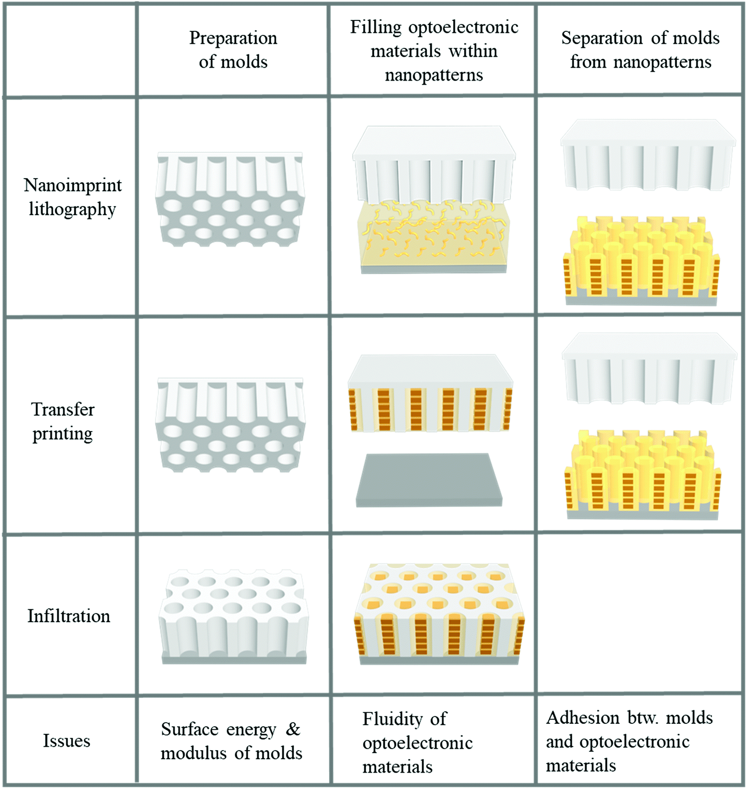
Two-dimensional nanopatterning methods, such as nanoimprint lithography, transfer printing after filling optoelectronic materials into nanopatterns, and infiltration into nanoholes, have been used to confine optoelectronic materials, such as conjugated polymers or perovskites, within nanoscale structures.21–23,25,141–159 In general, three steps are involved in 2D patterning methods for optoelectronic materials, as illustrated in Fig. 7. The first step is to prepare a mold with nanoscale structures. To obtain a nanoscale mold, e-beam lithography with a short wavelength to achieve high resolution followed by a dry etching process is conventionally used.135,136 This method can be used to fabricate designed structures such as lines and holes under the desired conditions; however, it requires sophisticated and expensive equipment. Self-assembly to obtain nanoscale patterns has also been employed for decades. Block copolymers (BCPs) have been used to create nanoscale patterns. The shape and size of patterns can be controlled by modulating the fraction and molecular weight of the constituent blocks within block copolymers. To fabricate a mold with nanoscale structure originating from self-assembled block copolymers, the control of surface chemistry on a substrate to manipulate the orientation of the nanoscale patterns, such as cylinders, is required.160,161 Dry etching process should follow the self-assembly of BCPs to transfer the BCPs to an inorganic substrate such as a silicon wafer, which is the limitation of using block copolymers to realize nanoscale molds. In addition to using ordinary BCPs as structural template, conjugated-amorphous BCPs can have a high degree of crystallization of phase-separated conjugated polymers by the nano-confinement of amorphous domains.162,163 Particularly, BCPs consisting of a solvophobic conjugated block and a solvophilic amorphous block can form highly-crystallized nano-colloids (e.g., nanofibril and nanoplatelet) in a selective solvent.164–167 Such self-assembled nanostructure of conjugated block polymers in thin films and solvents can generate enhanced electronic properties of conjugated polymers.
 | ||
| Fig. 7 Fabrication procedures for structural-template based confinements of optoelectronic materials. | ||
In the absence of sophisticated equipment such as photolithographic exposure equipment or a dry etcher to produce reactive ions, the formation of AAO can be one of the best candidates. Hexagonally ordered porous AAO can be prepared by two-step anodization.168,169 After the first anodization of aluminum films in an acid with a controlled voltage, the aluminum oxide is removed by another acid. During multiple anodization processes, AAO patterns with different shapes and sizes are obtained. Numerous research groups have used AAO as a master mold because of its low fabrication cost and the ability to create relatively large-area nanoscale patterns.168,169 The second step is filling functional materials into the void of the mold. Material fluidity and a driving force to move the materials into nanoscale holes are required to fill the optoelectronic materials into nanoscale structures. When a conjugated polymer is used, heat is applied to achieve fluidity. Organic materials, such as polymers, can be viscous when the temperature is above the glass transition temperature (Tg). For P3HT, however, the required temperature was substantially above the Tg because the crystalline structures were not movable around Tg.23,141 In addition, the applied pressure should be very high because the fluidity was not sufficient for filling. To achieve fluidity, many research groups have used additive-assisted nanoimprint lithography. They used a high-boiling point solvent or a small amount of polymeric additive to soften the optoelectronic materials even at room temperature. The driving forces, which are applied to fill a solution of functional materials into nanopatterns, are the external pressure and capillary pressure. The capillary pressure is given as below:
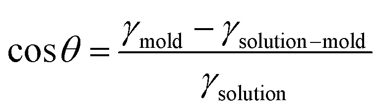
Pcapillary = 2γsolution![[thin space (1/6-em)]](https://www.rsc.org/images/entities/char_2009.gif) cosθ/r cosθ/r |
where γmold is the surface tension of a template/mold and γsolution–mold is the interfacial tension between a solution and a template. Given this relation, the capillary pressure can be higher when the surface tension of the mold surface is high, the interfacial tension is low, and the pattern size is small.
The final step of the two-dimensional patterning method is separation of the mold from the nano-confined optoelectronic materials attached to the substrate. Importantly, this final step is essential for maintaining the electronic properties of the functional materials. When a hard mold, such as silicon or AAO, is used to press the organic functional materials coated on a hard substrate, detachment of the mold from the substrate is difficult because they are bonded together too firmly.170 In addition, the mold surface should have a low surface energy to facilitate release of the nanoimprinted functional materials from the mold surfaces. Replica molding and a transfer method were proposed to resolve the issues of using nanoimprint lithography for nano-confinement of optoelectronic materials. When using a silicon wafer as a mold, pressure should be carefully applied to the substrate because it is very fragile. Replica molding is required to produce polymeric molds to use the silicon wafer as a mold.170–173 Thermoset polymers, such as PDMS, polyurethane (PU), polyurethane acrylate (PUA), and perfluoro-polyether (PFPE), were used as polymeric molds to fill functional materials within the nanoscale patterns.173,174 The Young's modulus should be high and the surface tension should be low to prevent lateral collapse between the structures to maintain nanoscale structures with a high aspect ratio.175 The modulus and surface tension can be modulated when preparing thermoset polymers by controlling the chain length, the number of acrylate groups for polymerization, and the fraction of fluorinated groups in the blend of copolymers.173 Although it is difficult to use a polymeric mold when the operating temperature is increased to provide optoelectronic material fluidity, a transfer method can be used when a solution of the materials is filled for the nano-confinement. When a solution of functional materials is coated on a replica mold, the solvent evaporates from the mold surface. After evaporation of the solvent from the mold, the mold containing the optoelectronic materials confined within the nanostructures is transferred onto the desired substrate. Importantly, the adhesion between the functional materials and the mold wall should be very low compared to the adhesion between the functional materials and the substrate surface to facilitate release of the nanostructures of the functional materials onto a substrate.176 The mold surfaces are treated by fluorinated self-assembled monolayers or low-surface-energy materials, such as PDMS and PFPE, which are used to achieve weak adhesion between the optoelectronic materials and the mold surface. Notably, the low surface tension of molds is contradictory to the condition of the high driving force by the capillary wetting discussed in the filling step. Therefore, the pattern size operates as an important factor for high capillary force regardless of adhesion issues. Even within impermeable molds, the capillary pressure could be higher than the atmospheric pressures in the nanoscale-level pattern size.177 In addition, optoelectronic organic materials should be attached to a polymer surface such as PEDOT:PSS, which is coated on a substrate to achieve adhesion and conductivity.
Aryal et al. used nanoimprint lithography to generate nanoscale structures with optoelectronic materials (Fig. 8A).21 They coated P3HT on a substrate and pressed it with silicon molds fabricated by conventional lithography followed by dry etching. They applied heat up to 170 °C to obtain P3HT film fluidity to fill the optoelectronic polymer into the nanosized grating and hole patterns. The images on the right in Fig. 8A are scanning electron microscopy (SEM) images of silicon molds (top) and nanoimprinted polymeric patterns (bottom).
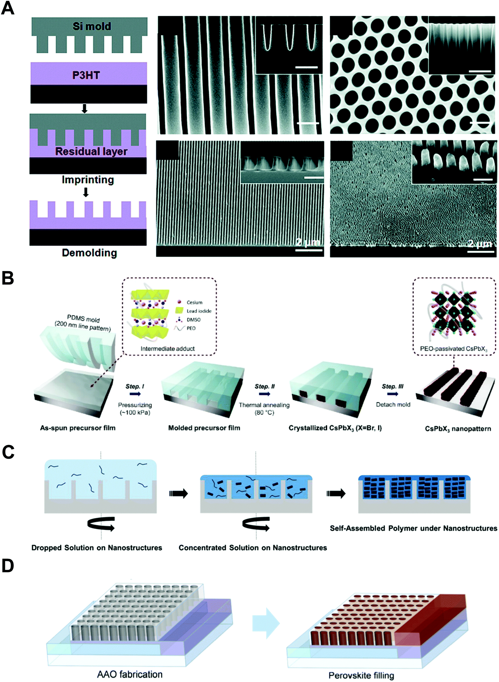 | ||
| Fig. 8 (A, left) Schematic illustrations of nanoimprint lithography of P3HT and SEM images of (right top) silicon molds and (right bottom) imprinted P3HT, (B) polymer-assisted nanoimprint of perovskite materials, (C) coating of optoelectronic polymers in nanoscale patterns, and (D) infiltration of perovskite precursors in AAO patterns. Adapted from ref. 21 with permission from American Chemical Society, copyright 2009, ref. 157 with permission from American Chemical Society, copyright 2020, ref. 148 under the terms of the Creative Commons CC BY license, copyright 2020 John Wiley and Sons, and ref. 151 with permission from John Wiley and Sons, copyright 2016, respectively. | ||
To achieve sufficient fluidity of the precursor films during nanoimprint lithography, high-boiling-temperature solvents such as dimethylformamide and N,N-dimethyl sulfoxide (DMSO) were added during the preparation of perovskite films. In addition, Jeong et al. incorporated a small amount (1%) of a polymer additive, such as poly(ethylene oxide) (PEO), into an inorganic halide perovskite (CsPbBr3) to make it moldable over a large area (Fig. 8B).156,157 After spin-coating the mixture of PEO and the precursor, the film remained in the soft state and could be deformed by imprinting it with a soft mold such as polydimethylsiloxane (PDMS). After nanoimprint lithography, the mold was removed by detaching it after crystallization of the perovskite material. Ko et al. demonstrated transfer printing of optoelectronic polymers confined in a nanoscale replica mold (Fig. 8C).148 This approach allowed preparation of various conjugated polymers under 2D nano-confinement. In particular, they also used a blend of P3HT and PTB7-th, which have different bandgaps to absorb light of different wavelengths, to enhance the crystallinity of the blend within the nanopatterns. They coated a solution of the polymer blend on a PFPE mold with nanoholes double replicated from AAO and allowed the solvent to evaporate slowly for crystallization with a favorable orientation. Another approach for endowing optoelectronic materials with fluidity is to fill functional materials as liquids and then solidify them within the nanostructures. When optoelectronic materials are filled in a liquid state, the applied pressure does not need to be high because the fluidity is sufficiently high. Kwon et al. used a mixed halide perovskite solution and coated it onto an AAO membrane fabricated on a conductive film.151 The nucleation density could be controlled by varying the concentration of the solution (Fig. 8D). Zhang et al. employed a similar procedure to form halide perovskite nanowires by a vapor–solid–solid reaction. They electrochemically deposited a metal Pb layer at the bottom of the AAO membrane and conducted the reaction with methylamine iodide vapor to form MAPbI3 nanowires confined in the AAO membrane.152
Nano-confinement of conjugated polymers by nanoimprint lithography or transfer printing has been achieved owing to the enhancement of the mobility by modulating the chain orientation from edge-on to chain-on or face-on alignment. Owing to the large hopping distance in the edge-on orientation, the charge (hole) mobility of P3HT is very low (10−10 cm2 V−1 s−1).142 In the case of chain-on or face-on alignment, in contrast, the hole mobility is very high (3.1 cm2 V−1 s−1) compared to that of edge-on orientation.143,146 Aryal et al. used nanoimprint lithography at a high temperature and high pressure to fill the optoelectronic polymers into nanosized grating patterns and suggested that the dominant orientation of P3HT was vertical orientation, and the degree of crystallinity increased after nanoimprint lithography of P3HT (Fig. 9A).21 Skrypnychuk et al. also explained that the chain-on (vertical chain)-oriented crystalline structures formed because of the shearing force of the viscous P3HT melt along the wall of the mold during the nanoimprinting process.143 Johnston et al. investigated P3HT crystallization in P3HT/PCBM blends infiltrated in nanogratings with widths of less than 200 nm.147 They used grazing incidence wide-angle X-ray scattering (GIWAXS) to examine the orientation of P3HT and found that the relative population of the edge-on orientation on flat surfaces was 30% and decreased to less than 5% when the blends were confined in nanogratings. Instead, the relative population of the face-on orientation was increased in the nanogratings, and the increasing tendency was higher for smaller grating widths.
 | ||
| Fig. 9 Schematic illustrations of (A) P3HT chain alignment during nanoimprint lithography (adapted from ref. 21 with permission from American Chemical Society, copyright 2009) and (B) chain alignment of polymer blends (P3HT & PTB7-th) after a transfer printing. (C) GIXD results of optoelectronic polymer nanopillars depending on different materials and diameters. Adapted from ref. 148 under the terms of the Creative Commons CC BY license, copyright 2020 John Wiley and Sons. (D) UV-Vis spectrum, GIWAXS results of CsPbI3 nanolines and SEM images of MAPbBr3 (left) and MAPbI3 (right) nanopatterns prepared by a polymer-assisted nanoimprint lithography. Adapted from ref. 157 with permission from American Chemical Society, copyright 2020. (E) Schematics of the crystallization mechanism of infiltrated inorganic perovskite precursors in different size of nanopatterns. Adapted from ref. 25 with permission from John Wiley and Sons, copyright 2019. | ||
Instead of using the Si or AAO templates that act as electrically insulating components in thin films, nanostructured inorganic semiconductors can be used for nano-confined templates as well as charge transporting layers. More specifically, vertically-aligned nanorods of inorganic semiconductors (e.g., TiO2, ZnO, GaN) have been incorporated into hybrid organic solar cells by the infiltration of conjugated polymers. For example, Letertre et al. prepared the array of vertically-aligned TiO2 nanorods with 200 nm height onto ITO substrates by magnetron sputtering method. After such process, P3HT-COOH was grafted onto the TiO2 nanorod surfaces through drop-casting, and then followed with rinsing with chlorobenzene to remove the excess layer of P3HT.178 Wang et al. reported the hybrid solar cells based on ZnO nanorods array. In this case, the ZnO nanorods with a height of 120 nm were formed on ITO substrates using hydrothermal method. Additionally, P3HT:PCBM blend solution was spun cast on the top of ZnO nanorods array.179 Recently, GaN nanowires array was also incorporated into P3HT:PCBM photoactive layer through spin-coating of P3HT:PCBM on GaN nanowires array.180 Although these hybrid systems can provide nano-confined environment during self-assembly of conjugated polymers, their nano-confinement effects have not been evidently identified.
Ko et al. performed systematic studies with grazing incidence X-ray diffraction (GIXD) on nanopillars of various geometric dimensions to investigate the crystalline structure and orientations of optoelectronic polymers (Fig. 9B).148 When the confinement dimension was smaller, the crystallinities of optoelectronic polymers, such as P3HT, PCDTBT, and PTB7-th, were increased, as shown by the strong π–π peaks in GIXD due to the strong nano-confinement effects induced by the interfacial interactions between the mold and the polymers (Fig. 9C).148 In the case of P3HT, the face-on orientation was increased to approximately 40 times compared to the population on a flat surface. The amorphous low-band gap polymers (PCDTBT and PTB7-th) also showed an increase in population of crystallites with face-on orientation. In addition, they examined the nano-confinement effect in nanocones and showed stronger crystallization at sharp tip areas. We note that the chain orientation changed dramatically to a favorable orientation in smaller nanopatterns regardless of the patterning method. The driving force of the shear force during nanoimprinting is a combination of external pressure and capillary force to fill the viscous melt into nanoscale structures. Because the capillary force is higher for small nanopatterns, the fraction of chain-on (vertical) orientation and the electrical mobility increase. As the pattern size decreases during coating of the solution onto a nanoscale pattern, evaporation within the nanostructures becomes slower, as predicted by the Kelvin equation.148 The hydrophobic polymer chains are then aligned to the surface of low-surface-tension molds under the thermodynamically favorable conditions, such as face-on orientation, due to the strong interfacial effect shown in thin film.
Jeong et al. investigated the nano-confinement effect on hybrid and inorganic perovskite materials fabricated by additive-assisted nanoimprint lithography.156,157 First, they used a high-boiling point solvent, such as DMSO, to obtain sufficient fluidity of the MAPbI3 and MAPbBr3 precursor films.156 After coating the precursor films on a substrate, the films were pressed with a PDMS mold at room temperature. Interestingly, a highly crystalline perovskite formed due to the slow evaporation of DMSO in the films within the nanopatterns. Additionally, they proposed polymer-assisted nanoimprint lithography to confine inorganic (CsPbI3) and hybrid (MAPbBr3 and MAPbI3) perovskite materials. They measured the UV-Vis absorbance of the nanopatterns and performed GIWAXS to confirm the formation of crystalline structures of cubic α-phase CsPbI3 (Fig. 9D).157 The lower part of Fig. 9D shows SEM images of MAPbBr3 and MAPbI3 fabricated by polymer-assisted nanoimprint lithography, which is an extension of polymer-assisted nanoimprint lithography for hybrid perovskite materials.
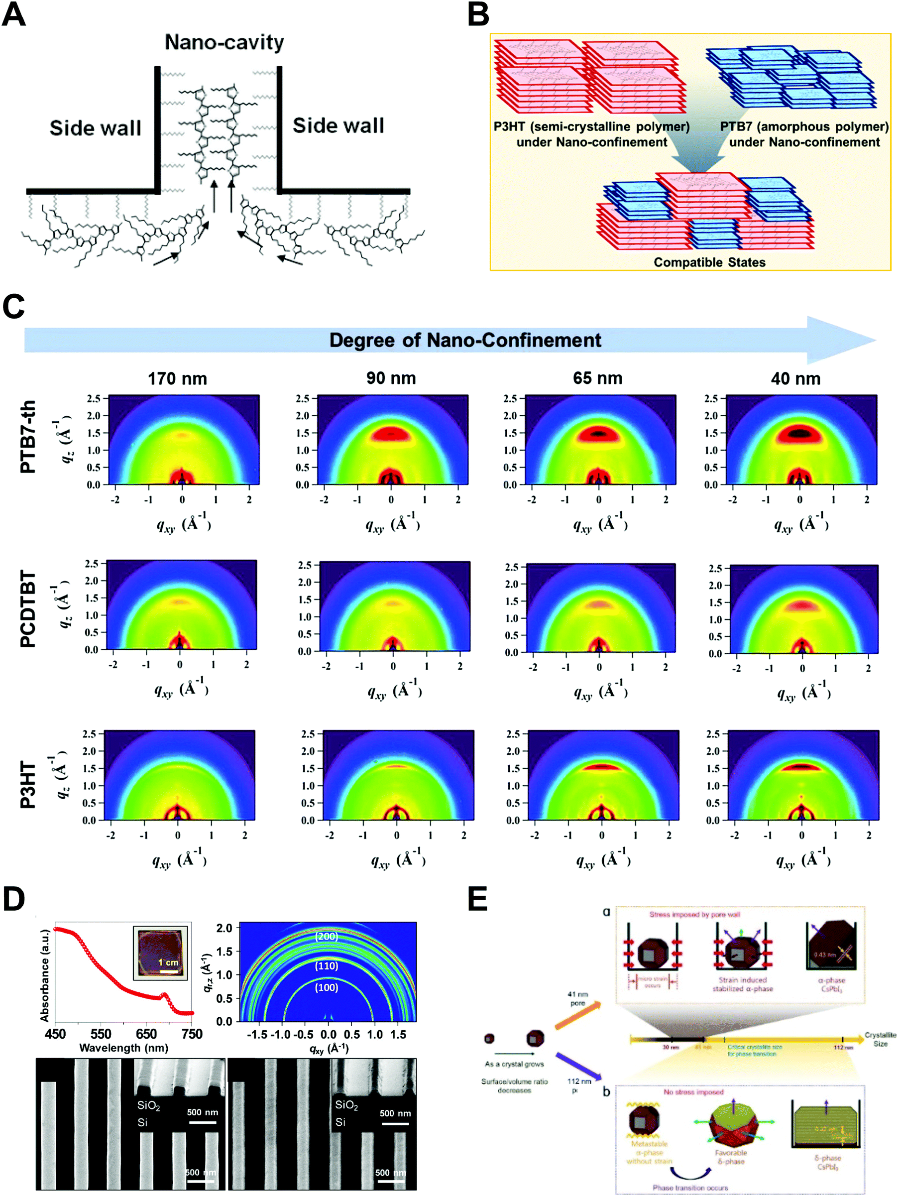
Ma et al. performed a systematic study on the strain-mediated stabilization of α-phase (cubic phase) α-CsPbI3 (Fig. 9E).25 CsPbI3 tends to form an inactive orthorhombic δ-phase under ambient conditions because of the small size of the cesium cation. Therefore, it has been essential to stabilize high-performance α-phase CsPbI3 under ambient conditions to improve device performance.25,29,181,182 The pore sizes of the AAO templates were controlled to control the degree of spatial confinement and manipulate the phase stability of CsPbI3, and the authors proposed a mechanism. When the pore size was small (41 nm), α-phase CsPbI3 crystals grew inside and maintained stability until the surface/volume ratio of the nanocrystals was sufficient, and the pore wall prevented the phase transition of the nanocrystals. In addition, anisotropic pores can lead to compressive strain in the perovskite lattice, which enhances the phase stability of α-CsPbI3. When the size of the AAO nanohole was 112 nm, α-phase CsPbI3 nanocrystals grew quickly without the strain effect and transformed into non-perovskite structures after the crystal size exceeded the critical point.
In this section, we discussed the previously reported assembly approaches for 2D nano-confinement and their effect on nano-confinement. Assembly approaches have been developed from fundamental studies on the effect of nano-confinement with nanoimprint lithography. For practical device fabrication on a large area, the mold materials should be flexible, and the operating temperature should be low to avoid deterioration of the device performance. To address these issues, additive-assisted fabrication methods have been proposed, but several limitations remain regarding the degradation of electronic properties. Therefore, transfer printing after infiltration of solutions and solvent-assisted nanoimprint lithography can provide insight into meeting the demand for practical assembly approaches of optoelectronic materials.
Nano-colloid state. The nano-colloid and composite states of perovskites have shown promise as advanced 3D confined systems for the application of optoelectronic devices. As described above, stabilizing the crystalline phase of perovskite nano-colloids under ambient conditions has been a critical issue for realizing high performance inorganic perovskite devices. For example, α-CsPbI3 nano-colloids with a cubic phase can be synthesized using long alkyl chains (oleic acid (OA) and oleylamine (OAm)) through hot-injection methods (Fig. 10A).26,183,184 The size of nano-colloids is easily controlled by changing the injection temperature within the range from 60 to 185 °C. Additionally, two-step purification can be used to obtain more stabilized CsPbI3 nano-colloids (Fig. 10B and C).185 These synthetic processes including surface-bound organic ligands significantly improved the phase stability of α-CsPbI3 nano-colloids, allowing the cubic phase to remain for a few months under ambient conditions.26 Moreover, additional ligand engineering of organic ligands bound to the bare surfaces of nano-colloids plays a critical role in determining the performance of optoelectronic devices. Although the surface-bound ligands can stabilize the cubic phase of CsPbI3, it should be noted that they can also notably hinder the charge transport between perovskite nano-colloids, which is closely related to the device performance.186 As a result, the size, interfacial interaction, and electronic and/or optical properties of organic ligands bound to nano-colloids should also be optimized to develop high-performance optoelectronic devices.
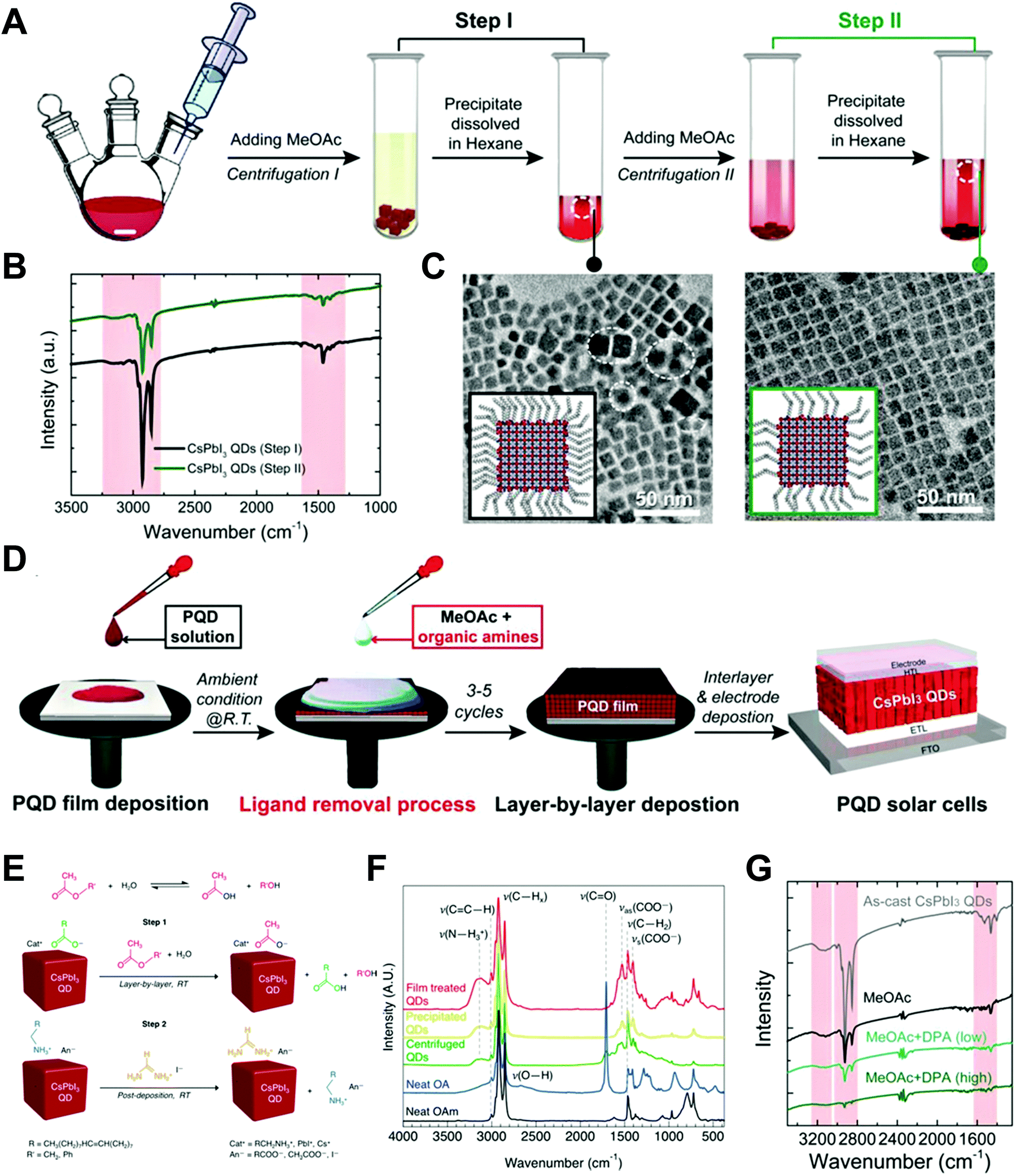 | ||
| Fig. 10 (A) Schematic illustration of synthesis of α-phase CsPbI3 nano-colloids. (B) FTIR spectra of CsPbI3 colloidal films based on step 1 purification and step 2 purification. (C) TEM images of step 1 purified and step 2 purified CsPbI3 nano-colloids. Schematic illustration of (D) procedures for fabricating CsPbI3 composite films by spin-assisted LbL assembly and (E) ligand-exchange reactions during the deposition process. (F) FTIR spectra of neat and MeOAc treated CsPbI3 colloidal films. (G) FTIR spectra of as-cast, MeOAc treated and MeOAc + DPA treated CsPbI3 colloidal films. (A–D and G) Adapted from ref. 185 with permission from John Wiley and Sons, copyright 2020 and (E and F) ref. 187 with permission from American Chemical Society, copyright 2018. | ||
Composite state. Among various assembly approaches for optoelectronic devices, spin-assisted LbL assembly has been widely applied to the preparation of perovskite nano-colloid-assembled composites (Fig. 10D).26,185–187 Specifically, in the case of CsPbI3 nano-colloidal composites, an alternating deposition process between spin-coating for hydrophobic CsPbI3 nano-colloids in octane and drop-casting (or dipping) for hydrophilic methyl acetate (MeOAc) treatment was repeatedly conducted on flat substrates until the desired thickness of the composites was reached. Generally, it is well-known that MeOAc solvent can effectively remove surface-bound organic ligands by ligand exchange reaction between native organic ligands and MeOAc (Fig. 10E–G).26,187 That is, perovskite nano-colloidal layers are deposited by spin-coating, and then, native organic ligands are chemically removed by MeOAc, which resultantly converts hydrophobic CsPbI3 nano-colloidal composites into hydrophilic composites. Based on these ligand engineering treatments, subsequent layers could be deposited without desorption of the underlying layers. However, this assembly process should be conducted carefully because excessive treatment with MeOAc induces agglomeration of hydrophobic CsPbI3 nano-colloids, and a further undesirable transition from the cubic phase to the unfavorable orthorhombic phase by destruction of the confinement environment. As a result, approximately 100 nm-thick CsPbI3 composites (from a CsPbI3 nano-colloidal solution with a concentration of 70 mg mL−1 in octane) can typically be deposited by a single step of the spin-assisted LbL assembly process (i.e., one LbL assembly process consists of spin-coating the CsPbI3 nano-colloid and MeOAc treatment). Although additional chemical treatments, such as formamidinium iodide186–188 or various organic amines,185 have been employed to further remove insulating native ligands from the composites, critical issues, such as conversion from native ligands to more effective and functional ligands, deposition onto various curved substrates beyond simple flat substrates and precise control of composite thickness per deposition layer, cannot be easily realized by these assembly approaches. Therefore, it is highly desirable that more versatile and effective assembly approach should be considered for the preparation of nano-colloidal composites for 3D nano-confinement.
4.2. Advanced composite fabrication using LbL and LE-LbL assembly
Among various approaches for preparing nano-confined organic, inorganic, or organic–inorganic nanomaterials, LbL assembly based on complementary interactions (i.e., electrostatic-, hydrogen-, or covalent-bonding interactions) between two different components has been considered as one of the most powerful and versatile solution-processable approaches.189–199 Since the first introduction of polyelectrolyte-based electrostatic LbL assembly by Decher and Hong in 1991,191 this LbL assembly approach has offered diverse opportunities to prepare vertically and laterally nano-confined multilayers with desired electrical, electrochemical, biological, optical and/or optoelectronic properties through delicate control of the film thickness, composition, and functionality on various substrates irrespective of their size and shape (Fig. 11A).200–211 Although the respective layers are alternately deposited onto the substrates, the formed multilayers exhibit an interdigitated interfacial structure rather than well-ordered, sharp interfaces between vertically adjacent layers due to insufficient surface coverage (i.e., low packing density of components per layer) in the lateral dimension, resulting in nano-blended films.212,213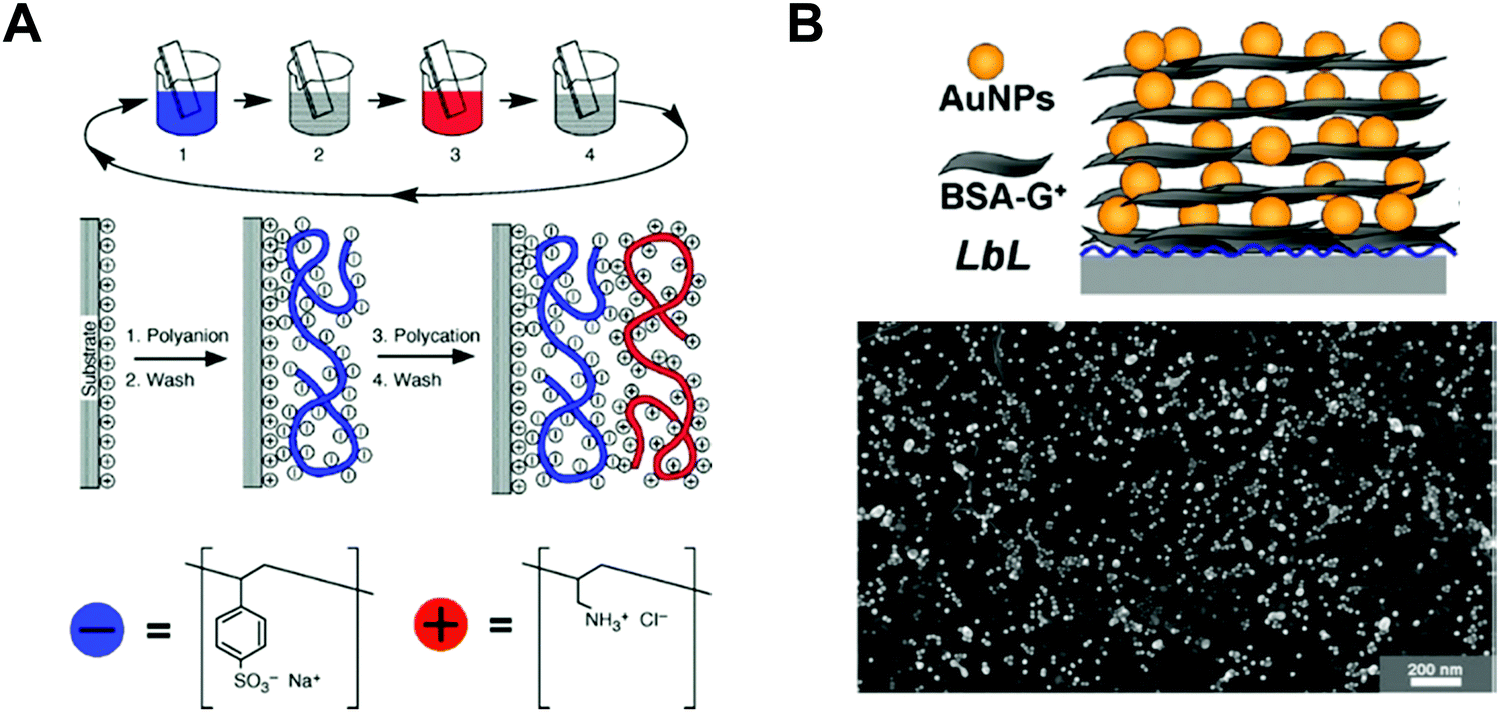 | ||
| Fig. 11 Schematic illustrations for the buildup of multilayer thin films via electrostatic interactions: (A) immersion of the charged substrate in the correspondent polyionic solution, alternating with washing steps; construction of the polyelectrolyte multilayers with n layers. Adapted from ref. 189 with permission from AAAS, copyright 1997. (B) Scheme for LbL-assembled multilayer films composed of anionic Au NPs and cationic bovine serum albumin (BSA)-functionalized graphene oxide nanosheets (BSA-G+) and SEM image of (BSA-G+/Au NP)n multilayers on Si-wafer. Adapted from ref. 214 with permission from American Chemical Society, copyright 2012. | ||
For example, negatively charged Au nano-colloids (Au NCs) can be consecutively LbL-assembled with positively charged polyelectrolytes using an electrostatic-interaction-induced LbL assembly in water (Fig. 11B).214 Although the packing density of charged Au NCs per layer in the lateral dimension can be further increased through pH control of the Au NC solution and the addition of an ionic salt as well as an increase in the Au NC concentration, the formation of densely packed NC films from aqueous NC dispersions is considerably restricted due to the strong electrostatic repulsion between NCs with the same charge, which, in most cases, results in a low surface coverage of less than approximately 30% (Fig. 11B).212–214 Moreover, the use of an insulating polyelectrolyte as a bulky polymer linker significantly increases the separation distance between vertically adjacent NCs as well as that between laterally adjacent NCs, which also has a detrimental effect on the charge transport between neighboring NCs.215–217 Particularly, given that this LbL assembly can be widely applied to various electronic, electrochemical, and/or optoelectronic devices, the charge transfer between neighboring functional nanomaterials within LbL-assembled films plays a critical role in determining the performance of the related functional devices.
Recently, a variety of conductive components (i.e., carbon nanotubes (CNTs), reduced graphene oxides, conducting polymers, metal NCs, and metal nanowires (NWs)) have been widely used for the preparation of LbL-assembled conductive films.203,207,215,216,218–221 However, numerous interface resistances (originating from the separation distance between conductive components, insulating organic ligands bound to the surface of conductive components, and/or bulky polymer binders or linkers) existing between neighboring conductive components have imposed a limit on the ability to sufficiently reveal the intrinsically high electrical conductivity of conductive components. For example, if highly conductive metal nanomaterials, such as Au NCs or Ag nanowires, are LbL-assembled with polymer linkers without the aid of thermal treatment and/or mechanical pressing, the formed films do not exhibit bulk metal-like electrical conductivity without thermal treatment, which is closely related to the interface resistances.216
A few years ago, Kim et al. reported that a free-standing conductive film could be prepared using LbL-assembled (anionic Au NC/cationic polyurethane)n=500 multilayers (i.e., 500 bilayer ∼ 1 laminated film or 1 × LbL), which exhibited an electrical conductivity of approximately 6.8 × 10³ S cm−1 after hot-pressing (at 120 °C and pressure of 20 MPa) (Fig. 12A and B).215 Additionally, when the number of laminated films was increased from 1 to 10 (i.e., 10 × LbL), their electrical conductivity was increased up to ∼104 S cm−1 and reached a plateau after 5 × LbL. However, considering that the electrical conductivity of the bulk Au film is approximately 4.1 × 10⁵ S cm−1 at 20 °C, the LbL-assembled film still exhibited a relatively low electrical conductivity, which also implied a number of contact resistances between neighboring Au NCs.
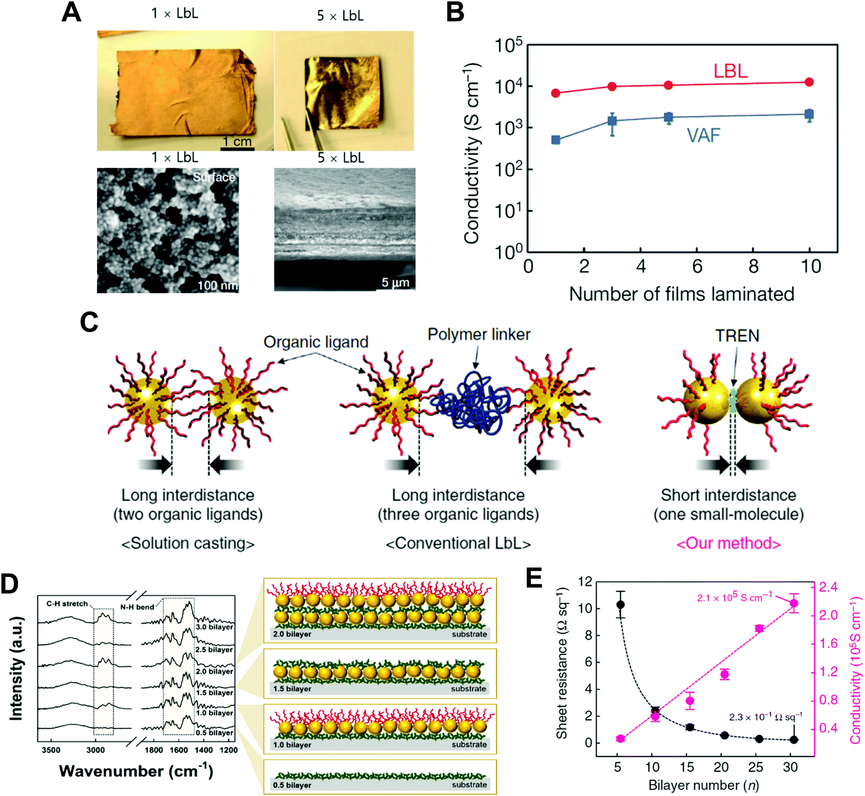 | ||
| Fig. 12 (A) Photographs and SEM-images of a free-standing film (PU/Au NP)500 (i.e., 1 × LbL) and 5 × LbL stack. (B) Conductivity data of laminated films composed of 1, 3, 5, and 10 consolidated films for LbL and VAF. Adapted from ref. 215 with permission from Springer Nature, copyright 2013. (C) Schematic diagram depicting the difference among the conventional solution casting of the metal NPs (left), traditional LbL assembly (middle), and small molecule linker-based LbL-assembly (right). (D) FTIR spectra and scheme of small molecule linker-based LbL-assembled (TREN/TOABr–Au NP)n multilayers as a function of the bilayer number (n). (E) Sheet resistances and electric conductivities of the (TREN/TOABr–Au NP)n multilayers coated onto quartz glass as a function of the bilayer number (n). Adapted from ref. 198 under the terms of the CC-BY Creative Commons Attribution 4.0 International License (https://creativecommons.org/licenses/by/4.0), copyright 2017 Springer Nature. | ||
As an alternative, Ko et al. reported that a small molecule linker-based LbL-assembly, which can induce a ligand exchange reaction between native ligands onto nanomaterials and small organic linkers during LbL deposition, could minimize the insulating barriers or interface resistances between neighboring nanomaterials (Fig. 12C–E).198 Specifically, tetraoctylammonium bromide (TOABr)-stabilized Au NCs in toluene were consecutively LbL-assembled with tris(2-aminoethyl)amine (TREN, Mw ∼ 146) in ethanol using complementary covalent-bonding interactions. In this case, the bulky TOABr ligands loosely bound to the surface of Au NCs were almost perfectly exchanged with amine (NH2)-functionalized TREN linkers due to the higher affinity of Au NCs with the NH2 groups of TREN during the repeated LbL assembly process (Fig. 12D). After such ligand exchange reaction, the organic layer existing between neighboring Au NCs buried within the LbL-assembled multilayers was only one TREN layer, inducing a tremendous decrease in the contact resistance between neighboring NCs. In the case of 30 bilayered film (i.e., (TREN/TOABr–Au NC)30 multilayers), it exhibited a metal-like electrical conductivity of 2.1 × 10⁵ S cm−1 and an extremely low sheet resistance of 0.23 Ω sq−1 without any thermal treatment and mechanical pressing (Fig. 12E), which were superior to those of metal nanomaterial-based conductors reported to date. That is, LbL assembly using a small-molecule-linker-induced ligand exchange reaction is very effective for enhancing or controlling the charge transfer within metal nanomaterial-based films. Further applications of LbL-assembled optoelectronic devices based on other electronically and/or optically active materials will be discussed in the following sections.
4.3. Nano-electronic characterization methods for nano-confined of optoelectronic materials
There have been only a few reports which have characterized the electronic properties of nano-confined materials, especially 2D-confined materials (see Tables 2 and 3). To comprehensively understand the electronic effects of nano-confinement, nanoscale as well as macroscale electronic characterization is necessary. Nanoscale imaging techniques combining electronic and topological information provide profound insights into the structure–electronic property relationship. To this end, SFM (also known as atomic force microscopy (AFM)) is one of the most promising tools for characterization (Fig. 13A). SFM enables a lateral resolution down to individual atoms. SFM can be operated in vacuum, liquids, inert atmospheres, and ambient conditions. The latter significantly simplifies the operation of the method and allows a variety of samples to be analyzed in their natural environments.| Confinement geometry | Assembly approach | Feature size | Electronic property (cm2 V−1 s−1) | Device performance | Ref. |
|---|---|---|---|---|---|
|
a IP: in-plane charge transport.
b OOP: out-of-plane charge transport.
c OPV: organic photovoltaic.
d PV: photovoltaic.
e 1:1 blend of P3HT and PTB7-th.
|
|||||
| 1D (one-face) | Spin-coating | <10 nm | (IPa) P3HT: <10−2 | — | 116 and 118 |
| (OOPb) P3HT: <10−4 | |||||
| Spin-coating on g-coated | 50 nm | (OOP) P3HT: ∼10−3 | — | 114 | |
| 1D (two-face) | Push coating | 100 nm | (OOP) P3HT: 0.47 | OPVc: 3.4% | 126 |
| 2D | Nanoimprint silicon mold (line) | 100 nm–560 μm | — | PVd: 3.43% | 142 |
| Nanoimprint AAO (pillar) | 150 nm | — | PV: 1.12% | 22 | |
| Nanoimprint PDMS (pillar) | ∼6 μm | (OOP) P3HT: 3.1 ± 0.7 | — | 143 | |
| Solvent-assisted nanoimprint silicon mold (line) | 50–210 nm | — | PV: 3.16% | 145 | |
| Solvent-assisted nanoimprint AAO (pillar) | 160 nm | — | PV: 1.85% | 146 | |
| Transfer printing PTFE (pillar) | 30–170 nm | (OOP) P3HT: 0.96 | — | 148 | |
| (OOP) PTB7-th: 0.036 | |||||
| (OOP) blende: 0.73 | |||||
| Confinement geometry | Assembly approach | Feature size | Electronic property (cm2 V−1 s−1) | Device performance | Ref. |
|---|---|---|---|---|---|
| a PD: photodetector. b Current efficiency. c EQE: external quantum efficiency. d FAI: formamidinium iodide. e DPA: di-n-propylamine. f MeOAc: methyl acetate. | |||||
| 1D (two-face) | Soft cover | 400 nm | — | MAPbI3 PV: 12.1% at 36.1 cm2 | 130 |
| 250 nm–2 μm | — | MAPbI3 PV: 15.5% at 5 cm2 17.7% at 0.09 cm2 | 131 | ||
| Hard cover | 10 μm | MAPbBr3 hole: 121 ± 15 electron: 36.8 ± 3.7 | MAPbBr3 PV: 17.8% | 132 | |
| 20 μm | — | MAPbI3 PV: 21.09% | 247 | ||
| 20 nm | — | MAPbI3 PDa: 5600 A W−1 | 249 | ||
| 2D | Infiltration AAO (pillar) | 10–400 nm | — | CsPbBr3 LED ∼0.09 cd A−1b |
150 |
| EQEc: ∼0.03%; | |||||
| Infiltration AAO (pillar) | ∼40 nm | — | MAPbI3−xClx PV: 13.23% | 151 | |
| Solvent-assisted nanoimprint silicon, PUA (pillar) | 200–500 nm | — | MAPbI3 PD: 34.7 A W−1 | 154 | |
| Additive-assisted nanoimprint PDMS (line) | 200–500 nm | — | CsPbI3 PD: 10−5 A W−1 | 157 | |
| Filling by asymmetric wetting chemical line pattern | 1000 nm | — | CsPbI3 PD: 1294 A W−1 | 158 | |
| Liquid phase transformation PDMS (line) | 735–1500 nm | — | MAPbI3 LED: 0.53 W (m2 sr)−1 | 159 | |
| 3D | Spin assisted LbL with nano-colloids | 150 nm | — | CsPbI3 PV: 10.77% | 26 |
| Spin assisted LbL with FAId treat | 100–400 nm | CsPbI3 (neat) 0.23 (FAI treat) 0.5 | CsPbI3 PV: 13.43% | 186 | |
| Spin assisted LbL with DPAe treat | 500 nm | CsPbI3 (MeOAcf only) 0.412 (DPA + MeOAc) 0.774 | CsPbI3 PV: 14.9% | 185 | |
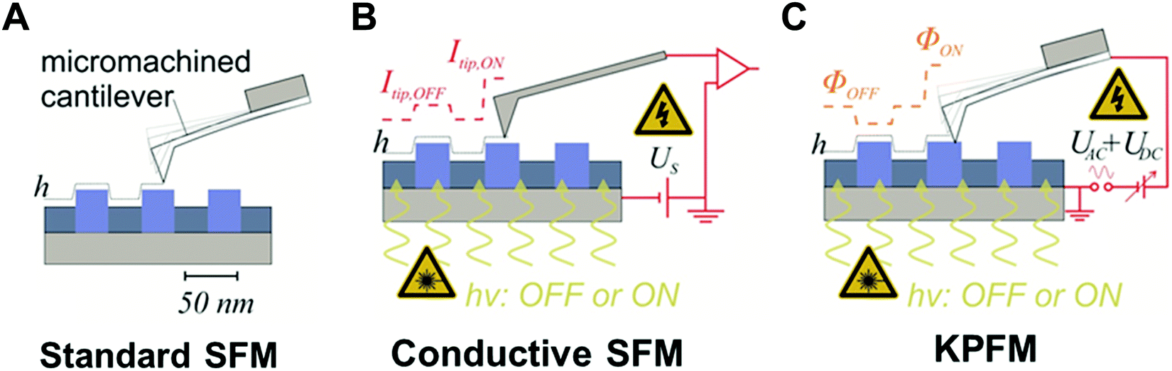 | ||
| Fig. 13 (A) Standard operation of scanning force microscopy (SFM): Illustrated is a micromachined cantilever having a tip at its end. By keeping the tip-sample forces constant, a height profile h can be recorded line-by-line. (B) Conductive scanning force microscopy (cSFM): conductive scanning force microscopy allows to measure the current flow between the tip and a nanostructure by implementing a voltage source and a current–voltage-amplifier between the cantilever support and the sample. Upon illumination with light (hν: ON), photo-excited charge carriers can be generated which increases the electrical current (Itip,ON). (C) In Kelvin Probe Force Microscopy (KPFM) an AC, as well as a DC potential is applied between tip and sample surface. When the sample is measured in dark (hν: OFF), the measured Kelvin probe signal corresponds to the work function difference between material A and B. When the sample is illuminated (hν: ON), the additional created surface charges are contributing to the measured signal. | ||
SFM has been widely used to investigate the surface topography from the μm scale down to the sub-nm scale. An atomically sharp tip is scanned over a surface line by line (Fig. 13A). When the tip comes close to the sample surface, it experiences the surface forces, leading to a deflection of the cantilever spring. Depending on the length, width, and thickness of the cantilever, spring constants from milli-N m−1 up to several tenths of N m−1 are commercially available. An electronic feedback circuit maintains a constant force between the tip and the sample surface by adjusting the tip-sample distance. For a comprehensive introduction to the plethora of SFM methods, the reader is referred to other books and reviews.222–225
Below, we will discuss SFM techniques that are useful for revealing confinement effects in optoelectronic materials. One of the main advantages of SFM is the possibility of using electrically conductive tips, which can probe local electronic properties on the nm scale. In particular, local optoelectronic properties can be studied in the dark and under light illumination. Below, we highlight the conductive SFM (cSFM) method (Fig. 13B) and the Kelvin probe force microscopy (KPFM) mode (Fig. 13C).
However, operating cSFM in contact mode can lead to mechanical damage of soft surfaces due to lateral forces while the tip scans. To reduce these lateral forces, new modes have been developed that excite the cantilever at its torsional resonance frequency. A more elegant approach brings the SFM tip periodically in contact with the sample surface (Fig. 14A). Such modes are called peak force or quantitative imaging modes and are implemented nowadays in most commercial instruments. (e.g., Peak Force and Quantitative Imaging Modes of Bruker, USA; Pin-Point Mode of Park Systems, Korea; Current Mapping with Fast Force Mapping of Oxford Instruments, USA). In addition, these modes allow to quantify adhesion and mechanical properties on nanometer scale.229 Particularly, detailed investigation of mechanical properties of thin films can often help understanding and measuring their electrical properties. In short, the tip vertically approaches the sample until a defined force setpoint, typically a few nN, is reached (Fig. 14A – step 1). Then, the tip is retracted again (step 2) and moved to the subsequent position (step 3). Then, the tip vertically approaches the sample again (step 4). As an example, we show a typical measurement of the force and current while a tip approaches a surface (Fig. 14B, corresponding to approach curve step 4, which is highlighted in red). When the tip touches the surface at a certain piezo position, a current is measured (red curve). This current increases with increasing normal force and reaches a maximum at the defined force setpoint. The maximum current value can then be used to represent the local conductance of a material. A conductance map is created by measuring the maximum current at each pixel of a topography image. This mode is essential for electronic characterization of fragile 2D-confined materials.228,230,231
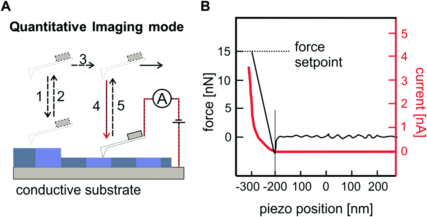 | ||
| Fig. 14 (A) Schematic illustration of the SFM tip that approaches the sample surface periodically. (B) The simultaneously recorded force and current can be plotted versus the piezo position. Current values are typically in the range between 1 pA up to 100 nA. The piezo position at which the conductive SFM-tip contacts the surface is marked with a vertical thin black line. | ||
Hole- and electron-accepting layers play a key role in optoelectronic applications. Zinc oxide (ZnO) is a transparent, wide bandgap semiconductor (3.3 eV). Importantly, ZnO can be processed from solution, allowing a large-scale roll-to-roll fabrication process.233 However, the orientation of ZnO nanostructures can influence the surface work function. Ultraviolet photoelectron spectroscopy (UPS) is routinely used to measure the work function of electronic materials. However, UV-illuminated areas typically have a diameter on the order of millimeters. Thus, work function variations on a smaller scale are overseen. Here, KPFM provides a means to analyze work function variations on the nm scale. Sharma et al. reported two distinct work function values separated by 0.1 eV on a sub-micrometer scale in nano-roughened, sol–gel-derived polycrystalline ZnO thin films.234 Heterogeneity in the work function of electron-accepting materials can significantly influence the interfacial charge transport across the materials.
KPFM also allows the detection of charging of the surfaces or interfaces of solar cell materials upon illumination. In this way, the photoresponse of bulk-heterojunction and perovskite surfaces has been investigated.235–237 Alternatively interfaces can be studied by breaking the cell and investigating the face side, i.e., the site of the fracture. However, simple breaking often creates a very rough surface on which KPFM cannot be performed at high resolution. Thus, the face side can be treated by ion milling to reduce the surface roughness. Bergmann et al. used KPFM to study the distribution of charges in mesoscopic MAPbI3 solar cells.238,239 These experiments were conducted in-operando, i.e., in the dark and under illumination. Under illumination and short-circuit conditions, holes accumulate in front of the hole-transport layer as a consequence of unbalanced charge transport in the device (Fig. 15A and B). This type of analysis was further refined by mapping the charge development upon a voltage pulse with sub-millisecond resolution.240 The authors reported the formation of a localized interfacial charge at the anode interface, which screened most of the electric field in the cell. In addition, the time-resolved measurements showed a contribution of mobile ions. In particular, the formation and release of interfacial charges is the dominant factor for current–voltage hysteresis. Schumacher et al. emphasized that the time resolution of charge detection is limited by the thermal noise in SFM.241 Using a pump–probe detection scheme allowed them to measure photocarrier decay times on the order of 1 ps for a GaAs sample.
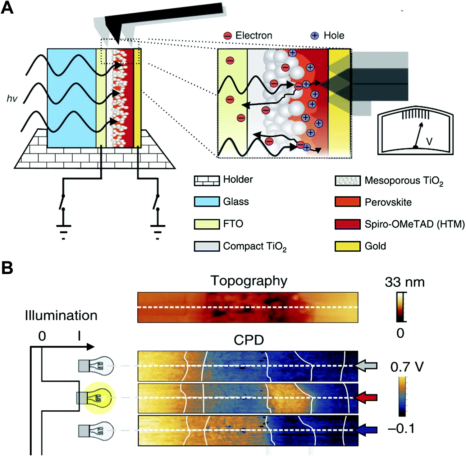 | ||
| Fig. 15 (A) Schematic illustration of SFM cantilever that scans the face side of a perovskite solar cell. (B) Topography and CPD maps of a perovskite solar cell under short circuit conditions, in dark and illuminated with light. Adapted from ref. 238 with permission from Springer Nature, copyright 2014. | ||
5. Conjugated polymers under nano-confinement
Various assembly approaches for nano-confinement (see Section 4.1) have provided an effective way to control the morphology of conjugated polymers in deposited states desirable for in-plane or out-of-plane charge transport. The enhancement of electronic properties, mainly the charge carrier mobility of P3HT, induced by various nano-confinement features and assembly approaches is discussed. Since P3HT has been widely employed as a model system material, it allows a comparison of the charge carrier mobility obtained by conventional approaches. In addition, although actual applications of optoelectronics devices are lacking, several preliminary optoelectronic devices prepared based on nano-confined materials are also described.5.1. Conjugated polymers under 1D nano-confined states
As previously discussed, varying the thickness of thin films by the spin-coating method, which corresponds to one-face 1D nano-confinement, had limitations in controlling the nano-morphology of conjugated polymers in the deposited states. Therefore, limited enhancement of charge mobility along both the in-plane and out-of-plane directions was achieved. In particular, significant challenges remain in increasing the charge carrier mobility along the out-of-plane direction.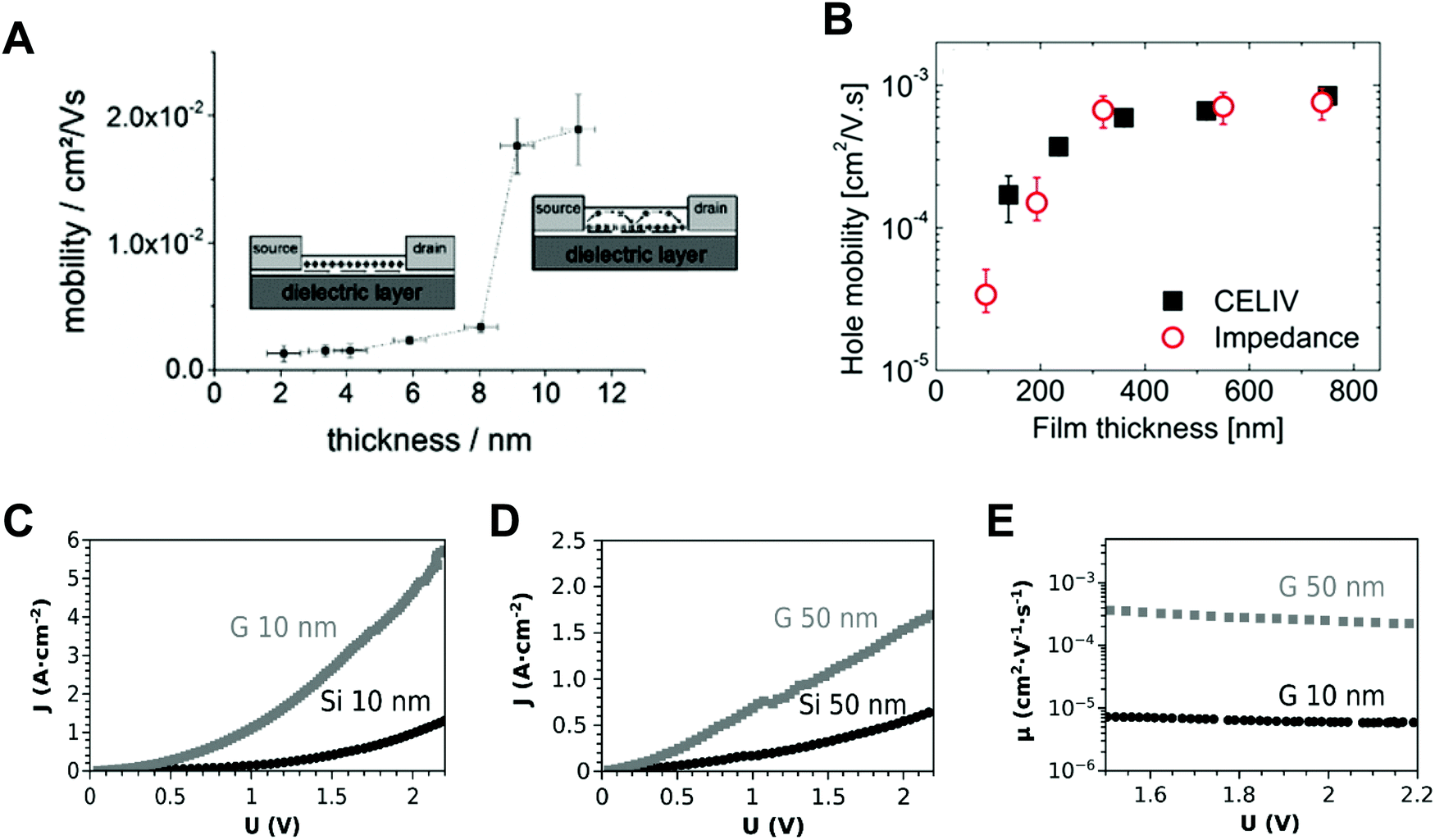 | ||
| Fig. 16 Film thickness dependent (A) in-plane and (B) out-of-plane charge carrier mobility of P3HT. Adapted from ref. 118 with permission from American Chemical Society, copyright 2017 and ref. 116 with permission from American Chemical Society, copyright 2013, respectively. Current density–voltage (J–V) characteristics of (C) 10 nm thick and (D) 50 nm thick P3HT films prepared on silicon (Si) and graphene. (E) Charge carrier mobility of 10 nm thick and 50 nm thick P3HT films prepared on silicon (Si) and graphene. Adapted from ref. 114 with permission from John Wiley and Sons, copyright 2014. | ||
5.2. Conjugated polymers under 2D nano-confined states
As discussed in Section 4.1.2, 2D nano-confinement is expected to be beneficial for out-of-plane charge transport based on preferential face-on or chain-on orientation of conjugated polymers. However, only a few examples of electronic properties and device performances have been reported, as summarized in Table 2. In this section, we discuss the effect of nano-confinement on conjugated polymers based optoelectronic devices such as photovoltaics. Conjugated polymers, such as P3HT, have received considerable research attention for organic photovoltaics because of the potential for large-area fabrication by the roll-to-roll process to achieve a low fabrication cost. The high charge mobility of P3HT is required to achieve a high-PCE over a large area in photovoltaic devices.The general procedure for the fabrication of photovoltaic structures confined in nanoscale structures is shown in Fig. 17A.146 After preparing a mold, a P3HT thin film coated on a PEDOT:PSS/indium tin oxide (ITO)/glass substrate was pressed by the mold. Ding et al. used solvent-assisted nanoimprint lithography to fabricate P3HT pillars at room temperature.146 After preparing the P3HT nanopillars, PCBM was spin-coated onto the pillars. PCBM was used as an acceptor material for a photovoltaic cell. Then, LiF and metal electrode were deposited on the PCBM. The ordered bulk heterojunction (OBHJ) photovoltaic cells were expected to be reproducible and well controlled. We note that the AAO mold should be removed after nanoimprint lithography. To release the AAO mold from the P3HT pillars, the AAO surface was treated with fluorinated materials. OBHJ cells with P3HT pillars of various diameters (OBHJ-100:100 nm, OBHJ-60:60 nm, and OBHJ-45:45 nm) were fabricated, and the performance of the photovoltaic devices was evaluated (Fig. 17B).146 The open-circuit voltages (Voc) were 0.50–0.51 V and were uniform throughout all the devices. In contrast, the short-circuit currents (Jsc) of cells with nanoconfined P3HT pillars (6.94 mA cm−2) were improved compared to that of the planar heterojunction (PHJ) (3.80 mA cm−2) due to the face-on orientation of P3HT within AAO nanoholes. External quantum efficiency (EQE) curves represented a broad response from 300 to 700 nm wavelength, and photovoltaic cells with a smaller diameter could achieve higher EQEs throughout the visible range due to the efficient transport of exciton. Lu et al. used P3HT/PCBM blends to perform nanoimprint lithography (Fig. 17C).141 They compared nanoimprinted P3HT/PCBM to pure P3HT and explained that the overall P3HT chain reorientation is greater in the blends. In addition, they showed significant polymer chain orientation during nanoimprinting at 150 °C compared to that at 100 °C. They claimed that face-on reorientation is induced due to the increased side-wall interfacial area at higher temperatures. The low-surface-energy groups at the interface led to rearrangement of the hexyl group. They measured the J–V characteristics with photovoltaic devices.141 When nanoimprinting was performed at 100 °C, no significant improvement occurred in the PV performances, such as Jsc and Voc, compared to that of planar devices. In contrast, when the blends were imprinted at 150 °C, the PCE was increased from 1.9% to 2.3% compared to that of the sample imprinted at 100 °C due to the improvement of charge carrier extraction by chain reorientation. The limitation of the estimation of the charge mobility from PV devices is that the PCE is low even compared to that of bulk heterojunction photovoltaic cells due to a lot of energy loss mechanisms. Skrypnychuk et al. proposed a method to measure the vertical charge mobility directly by applying a potential difference U between two conductive electrodes (Fig. 18A).143 They measured the macroscopic current density across the film and divided the current by the total area of the top surface of the pillars. They imprinted P3HT with a PDMS mold at 200 °C for 5 min, and the measured out-of-plane mobility of P3HT was 3.1 cm2 V−1 s−1 (Fig. 18B). They attributed the high mobility to the vertical (chain-on) orientation due to the shearing force during nanoimprint lithography. Ko et al. used transfer printing to confine homopolymers as well as polymer blends and measured the conductivity by scanning the entire area (Fig. 18C).148 They characterized both the nanoscale and macroscale electronic properties of a semicrystalline (P3HT), an amorphous polymer (PTB7-th), and a blend of P3HT and PTB7-th as a function of the diameter of the nanopillar. The conductivity increased considerably with decreasing diameter of the nanopillars of conjugated polymers from 170 to 40 nm, which corresponds to an increase in the fraction of face-on orientation. The trend of the enhancement in conductivity with nano-confinement was identical for the semicrystalline polymer (P3HT), the amorphous polymer (PTB7-th), and the blend of P3HT and PTB7-th. Higher absorbance of the imprinted samples was observed via UV-Vis spectroscopy (Fig. 18D) and higher mobility was demonstrated by the measured I–V characteristics (Fig. 18E). The out-of-plane charge mobilities of nanopillars with P3HT, PTB7-th, and the 1:1 blend were 0.96, 0.036, and 0.73 cm2 V−1 s−1, respectively. The increased vertical mobility corresponded to the GIXD results, showing an increase in the face-on orientation in the nanopillars.148
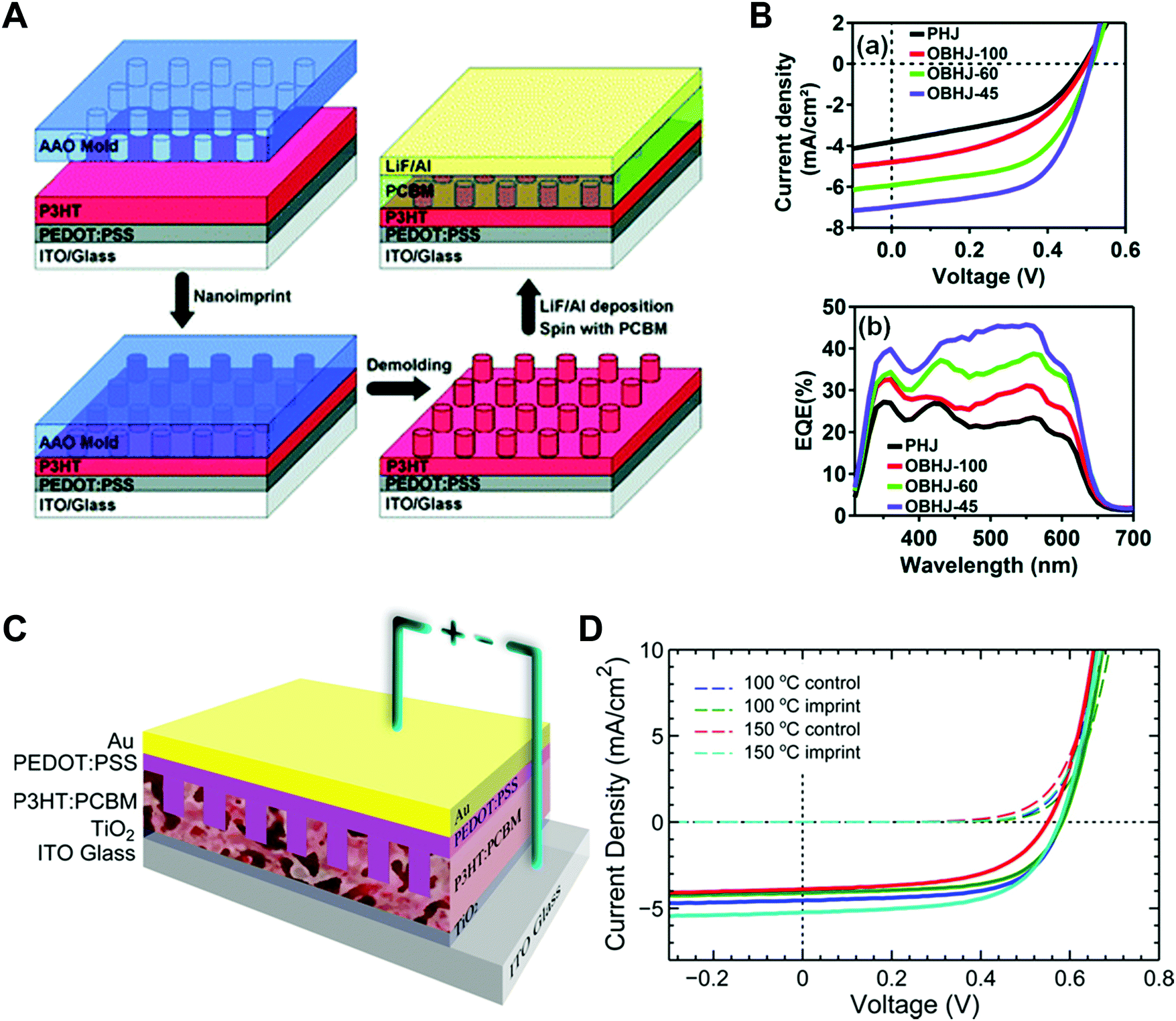 | ||
| Fig. 17 PV applications with conjugated polymers. (A) Schematic illustration of solvent assisted nanoimprint lithography for P3HT to fabricate ordered bulk heterojunction (OBHJ) photovoltaics. (B) J–V and external quantum efficiency (EQE) curves of planar heterojunction (PHJ) and OBHJ photovoltaics. Adapted from ref. 146 with permission from Royal Society of Chemistry, copyright 2015. (C) Schematic illustration of a photovoltaic cell after imprinting a P3HT/PCBM blend film. (D) J–V curves of devices imprinted at different temperatures. Adapted from ref. 141 with permission from American Chemical Society, copyright 2015. | ||
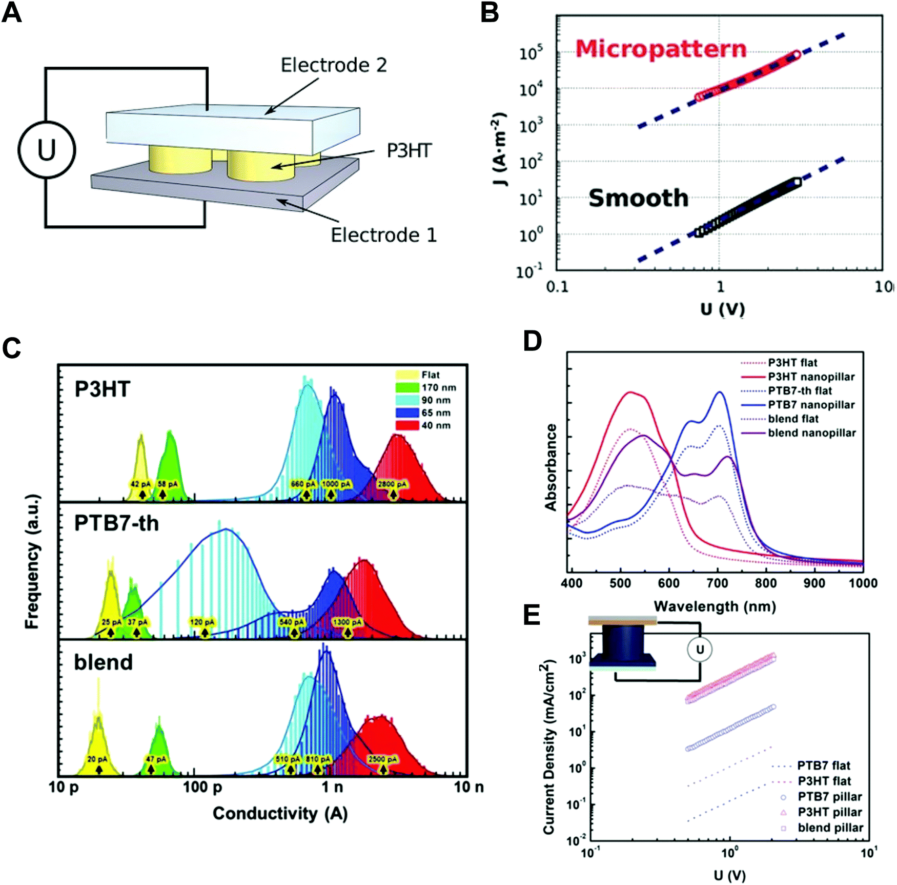 | ||
| Fig. 18 (A) Schematic illustration of the setup for macroscopic measurements of imprinted samples. (B) Plots of vertical current density in a smooth film, and in a patterned film of P3HT. Adapted from ref. 143 with permission from John Wiley and Sons, copyright 2016. (C) Conductance histograms of nanopillars consisted by P3HT, PTB7-th and 1:1 blends after a transfer printing. (D) UV-Vis results of samples in different conditions. (E) Plots of vertical current density in flat and patterned samples. Adapted from ref. 148 under the terms of the Creative Commons CC BY license, copyright 2020 John Wiley and Sons. | ||
5.3. Nanoscale characterization by SFM methods
The local electronic properties can be investigated with SFM methods. Skrypnychuk et al. conducted cSFM measurements in contact mode on pillars composed of P3HT that were several μm in diameter.143 The measured cSFM current map evidently showed different local conductivities at different positions. On top of the pillars, a current was measured, while between the pillars, i.e., in the flat areas between the pillars, the current was significantly decreased. The different current flow is attributed to the nano-confinement of P3HT. Moreover, the edge areas of the pillars showed the highest conductance, even higher than the value measured in the central area of the pillars. This observation is thought to originate from interactions at the side wall of the template, which consistent with the nano-confinement effect on the electronic properties. On the other hand, the highest conductance values were always oriented along the scanning direction. Therefore, the conductance map could also simply be an artifact related to the conical tip shape leading to larger contact areas at the edge of the pillars beyond the effect attributed to elastic deformation.When the diameter of conjugated polymer pillars is less than 100 nm with a higher aspect ratio, free-standing, vertically aligned, conductive nanostructures can be very fragile. Such structures bend and break while scanning with the SFM-tip in contact mode. Weber et al. used scanning conductive torsion mode microscopy to characterize the local conductivity in fragile free-standing nanopillar arrays (Fig. 19A and B).245 These polymeric pillars were fabricated by using an AAO template. Individual nanopillars were studied, and the current–voltage dependence suggested space-charge-limited conduction in the semiconducting nanopillars. In a recent publication, Ko et al. used the quantitative imaging mode to show that the vertical electrical current increased by more than 50 times when the pillar diameter was decreased from 170 to 40 nm (see Fig. 18C).148 The authors attributed this behavior to enhanced crystallinity corresponding to the face-on orientation of conjugated polymers. The enhanced crystallinity was a direct result of the increase in confinement by fabricating thinner pillars.
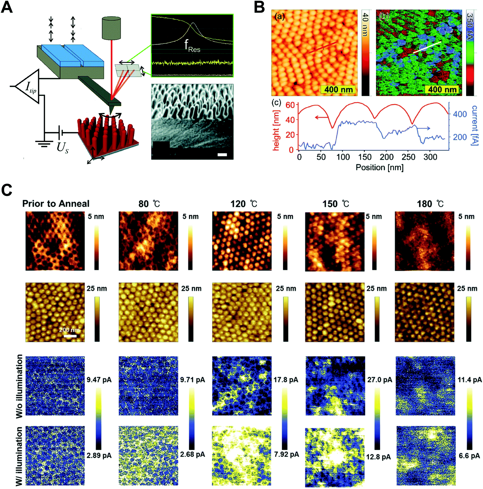 | ||
| Fig. 19 (A) Schematics of scanning conductive microscopy with torsional mode. The tips oscillate laterally over the sample because of the torsional movement of the cantilever. (B) Topography and current map of conjugated polymer (thermally cross-linked N,N′-bis(4-methoxyphenyl)-N,N′-bisphenyl-(1,1′-biphenyl)-4,4′-diamine (TPD) derivative) nanopillar arrays measured by scanning conductive torsion mode microscopy. Adapted from ref. 245 with permission from American Chemical Society, copyright 2010. (C) Height and conductivity (in dark state and illuminated state) images of nanostructured P3HT/PCBM prepared at different annealing conditions. Adapted from ref. 246 with permission from John Wiley and Sons, copyright 2016. | ||
In addition, heterojunction solar cells have been prepared by nanoimprinting the electron-donor polymer P3HT.246 The spaces between the electron-donor polymer (P3HT) were filled with PCBM, which is an electron-acceptor material. A subsequent annealing step allowed interdiffusion of both materials. This process led to vertically aligned, bulk heterojunctions. For these heterojunction structures, cSFM was used to study current transport in the dark and upon illumination. A clear relationship between the nano-morphology and the microelectronic properties and device performance was observed (Fig. 19C). Thus, cSFM can be used to evaluate the success of a donor–acceptor morphology without the need to fabricate a working device.
6. Perovskites under nano-confinement
The crystalline structures of hybrid and all-inorganic perovskites can be significantly influenced by nano-confinement based assembly approaches, which is expected to result in enhanced electronic properties as described in Section 4.1. The electronic properties of perovskites modulated by various assembly approaches of different nano-confinement features are discussed based on the charge carrier mobility, diffusion length, and performance parameters of the optoelectronic devices.6.1. Perovskites under 1D nano-confined states
Assembly approaches based on two-face 1D confinement have been successfully applied to perovskite materials, resulting in highly enhanced electronic properties. Soft-cover methods enabled formation of dense and pinhole-free perovskite films with large crystal grains over a large substrate for application in photovoltaic devices.129–131 They reported MAPBI3 photovoltaics with an efficiency of 12.1% at 36.1 cm2130 and 15.5% at 5 cm2,131 which were the highest efficiencies for the measured areas.
In addition to soft-cover based 1D confinement, Chen et al. reported the two hard substrates based 1D confinement assembly approach that can result in single-crystalline thin films of MAPbI3.132,247 The hole and electron mobilities of the single-crystalline thin films were reported to be 121 ± 15 cm2 V−1 s−1 and 36.8 ± 3.7 cm2 V−1 s−1, respectively, which were comparable to those of bulk single crystals. In addition, the hole diffusion length and electron diffusion length were 24.7 and 13.6 μm, respectively, which were greatly increased compared to those of polycrystalline perovskites. The PCE of the best device also increased to 21.09% with a Jsc of 23.5 mA cm−2, a Voc of 1.08 V, and a FF of 83.5%,247 compared to the efficiency of approximately 4% for previously reported single-crystalline thick perovskite-based solar cells.44,248 Notably, the flexible photodetector composed of ultrathin (thickness of 20 nm) single-crystalline MAPbI3 exhibited a significantly enhanced responsivity of 5600 A W−1, which is more than 2 orders of magnitude higher than that of previously reported flexible perovskite photodetectors.249
6.2. Perovskites under 2D nano-confined states
2D nano-confined perovskite materials have been used to fabricate optoelectronic devices such as photodetectors, photovoltaics and LEDs. Confinement led to improvement of the crystallinity and stability of the perovskite devices. Wang et al. demonstrated the nanopatterned photodetector with improved crystallinity and optical properties (Fig. 20A).154 They used solvent-assisted nanoimprint lithography. After preparing a silicon mold (line pattern, pitch = 275 and 600 nm), they pressed the mold against a MAPbI3 film coated on a SiO2 surface at 100 °C and a pressure of 7 MPa. They investigated the effect of nanoimprint lithography on crystallization by SEM and X-ray diffraction (XRD). The grain boundaries disappeared, and the crystallite sizes increased from 68 to 188 nm after nanoimprinting. After the deposition of Au films onto the nanograting, perovskite photodetectors were fabricated to examine the effect of nano-confinement on the photodetector performance, such as responsivity versus irradiance at λ = 635 nm (bias voltage = 1 V). The responsivity generally decreased with increasing light irradiance. Interestingly, the responsivity of the nanograting photodetector at 2 nW cm−2 was 6.2 A W−1, which is much higher than that of the thin-film photodetector. At an irradiance of 4.5 nW cm−2, the responsivity of the nanograting photodetector was 58.5 A W−1, which is much higher than that of a commercial photodetector.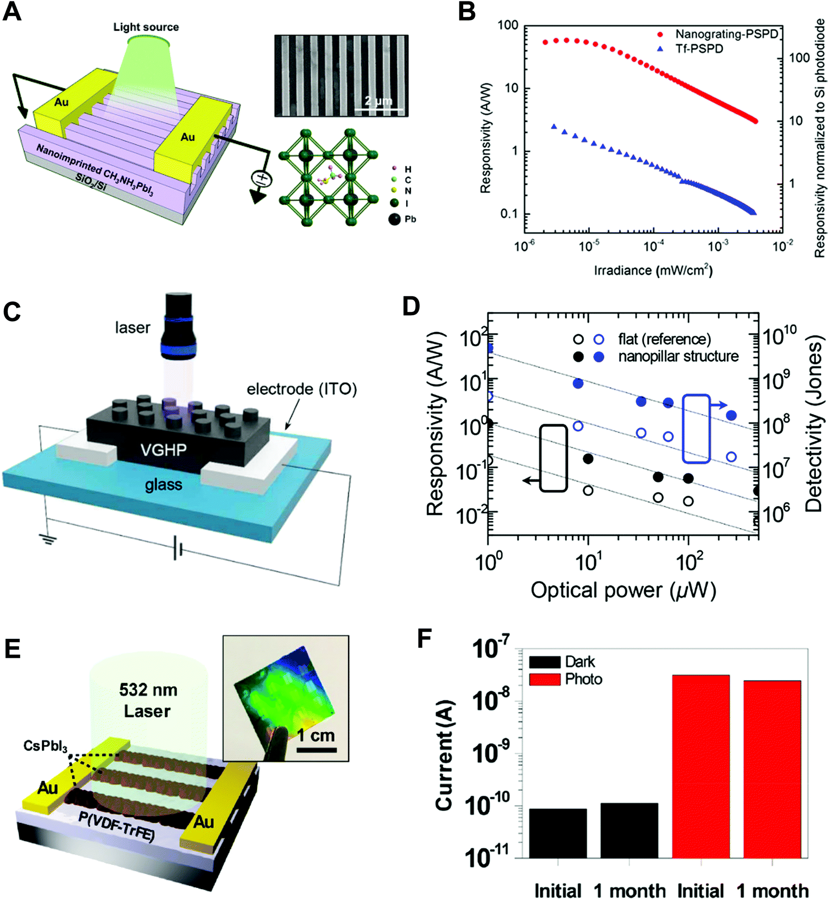 | ||
| Fig. 20 Photodetector applications with perovskite materials. (A) Schematic illustration and SEM image of nanograting a perovskite photodetector. (B) Plot of irradiance-dependent responsivity at λ = 635 nm. Adapted from ref. 154 with permission from American Chemical Society, copyright 2016. (C) Schematic illustration of a vertically grown halide perovskite (VGHP) photodetector. (D) Plots of responsivity and detectivity of flat and VGHP photodetectors. Adapted from ref. 153 with permission from American Chemical Society, copyright 2018. (E) Schematic and photographic image of a parallel type photodetector fabricated by polymer-assisted nanoimprinting of CsPBI3 and backfilled by PVDF-TrFE. (F) Dark and photocurrent of a device before and after a month showing the stability. Adapted from ref. 157 with permission from American Chemical Society, copyright 2020. | ||
Chun et al. also fabricated a photodetector by nanoimprinting MaPbI3 films (Fig. 20C).153 They prepared a two-terminal photodetector with patterned ITO electrodes. After spin-coating MAPbI3 films on the ITO surfaces, they stamped a polyurethane acrylate (PUA) mold against the perovskite films at 100 °C. During the imprint procedure, the MAPbI3 film was crystallized. They investigated crystallization by XRD and found that nano-confinement improved the crystalline orientation. The responsivity and the specific detectivity of the nano-confined perovskite films were improved by an order of magnitude compared to those of flat films (Fig. 20D).153 When the optical power was 1 μW, the responsivity and specific detectivity of the photodetector with a vertically grown hybrid perovskite material were 1 A W−1 and 5 × 10⁹ Jones, respectively.
Jeong et al. fabricated photodetectors after molding a soft perovskite precursor film with a polymer additive, which exhibited environmental and phase stability after overcoating with polyvinylidene fluoride-co-trifluoroethylene (PVDF-TrFE) by confining crystallization (Fig. 20E).157 They prepared two parallel Au electrodes (channel length = 50 μm) and patterned CsPbI3 with a PDMS mold (580 nm period) by polymer-assisted nanoimprint lithography. They irradiated the devices with a laser with a wavelength of 532 nm, which can be absorbed by α-phase CsPbI3. Although the responsivity was low (10−5 A W−1) compared to the results reported by other groups, the photocurrent remained stable before and after storage for 1 month (humidity = 40%, excitation power = 81 mW, bias = 5 V).
Demchyshyn et al. used nano-confined perovskite crystals to improve the LED performance (Fig. 21A).150 They infiltrated perovskite precursor solutions into nanoscale membranes fabricated on a substrate and then induced crystallization in nano-confinement. The confinement of perovskite materials within nanostructures, such as nanoholes and nanogratings, can shift the photoluminescence emission to shorter wavelengths. For example, infrared-emitting materials, such as MAPbI3, become visibly red and green-emitting materials, such as CsPbBr3, show blue emission. The perovskite quantum wire fabricated by infiltration within an AAO membrane showed significant enhancement of the internal photoluminescence quantum yield and light out-coupling. Owing to the blue-shifted photoluminescence and conductivity enhancement of perovskite nanostructures, performance improvement of LEDs, and photodetectors were demonstrated after nano-confinement. Optical devices, such as LEDs, were fabricated after infiltration of perovskite materials into AAO membranes prepared as insulating layers of transparent conductive films to exploit the vertical electrical property enhancement. A nanoporous AAO membrane was obtained after deposition of a bilayer of Ti and Al and the precursor solution was filled into the pores to produce nanocrystals. Subsequently, a hole transport layer (HTL) and MoOx/Ag electrodes were deposited onto the nanocrystals. The electroluminescence of the CsPbBr3 LED device was demonstrated, with a sharp green/cyan color (Fig. 21B). Kwon et al. also demonstrated a red-emitting LED device with a configuration of Au/spiro-OMeTAD/CsPbI3 confined within AAO membrane/TiO2/FTO/glass (Fig. 21C).151 They also used a similar device structure to fabricate semitransparent photovoltaic devices. The AAO height and the thickness of the perovskite films were controlled. The open-circuit voltage (Voc) and the short-circuit current (Jsc) were increased in perovskites films with a greater thickness, and the PCE was 13.27% (Fig. 21D). Moreover, the long-term stability of the photovoltaic devices was improved due to the suppression of ion migration in the perovskite nanopillars.
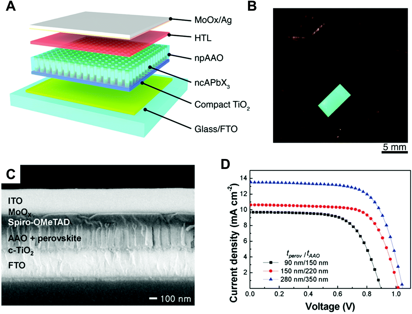 | ||
| Fig. 21 LED and PV applications with perovskite materials. (A) Schematic illustration of a LED fabricated by the infiltration of nanocrystalline perovskite materials within nanoporous AAO. (B) Photographic image of a LED displaying cyan-green light over the pixel. Adapted from ref. 150 under the terms of the CC BY-NC, Creative Commons Attribution NonCommercial License 4.0 (https://creativecommons.org/licenses/by-nc/4.0), copyright 2017 AAAS. (C) Cross-sectional SEM image of a photovoltaic cell prepared by the infiltration of a perovskite material within an AAO template. (D) J–V curves of devices with different layer thicknesses. Adapted from ref. 151 with permission from John Wiley and Sons, copyright 2016. | ||
6.3. Composite states with perovskite nano-colloids
As described in Section 4.1.3, α-CsPbI3 nano-colloids with favorable optoelectronic properties can be formed into composite states by spin-assisted LbL assembly. Initially, Swarnkar et al. reported that a 150 nm-thick CsPbI3-assembled composite for photovoltaic applications could be prepared by repeating the processes of spin-coating of α-CsPbI3 nano-colloids and chemical treatment of MeOAc.26 The resultant photovoltaic devices exhibited a PCE of 10.77%. However, the device performance of this CsPbI3 composite was lower than those of other CsPbI3-based devices, mainly because of the relatively low short-circuit current density (Jsc) arising from the inferior carrier transport in the composite. Since the presence of insulating ligands bound to the surface of nano-colloids has an adverse effect on the charge carrier transport within composites, additional chemical treatments are required to further remove the residual bulky ligands from the perovskite nano-colloidal composites.Several groups reported that the PCE of CsPbI3 nano-colloidal composite-based devices could be increased up to above 12%186,187 by an aid of the additional treatment with formamidinium iodide (FAI) on the neat MeOAc-treated CsPbI3 composite, which was mainly due to the enhanced charge carrier mobility (Fig. 22A and B).186 Wang et al. also investigated the effects of various organic amine-based treatments on the device performance.185 Additionally, they reported that treatment of the CsPbI3 composite with a combination of MeOAc and di-n-propylamine (DPA) could further remove residual native ligands (i.e., OA and OAm). Based on this treatment, the enhanced charge carrier mobility resulted in a high PCE of 14% (Fig. 22C and D). However, it should be noted that the spin-coating-based assembly methods without a washing process after nano-colloids deposition resulted in thick deposition of nano-colloids (∼100 nm) per each step (i.e., spin-coating of solution and MeOAc treatment), which led to considerable difficulty in investigating charge transport within a few nanometer-level thickness. In this view, if ligand-exchange reaction-mediated LbL (see Section 4.2) allowing precise control of the nanometer thickness can be applied to the preparation of perovskite nano-colloidal composites, we envision that more detailed and systematic studies on charge transport within perovskite composites will be performed for development of high-performance optoelectronic devices.
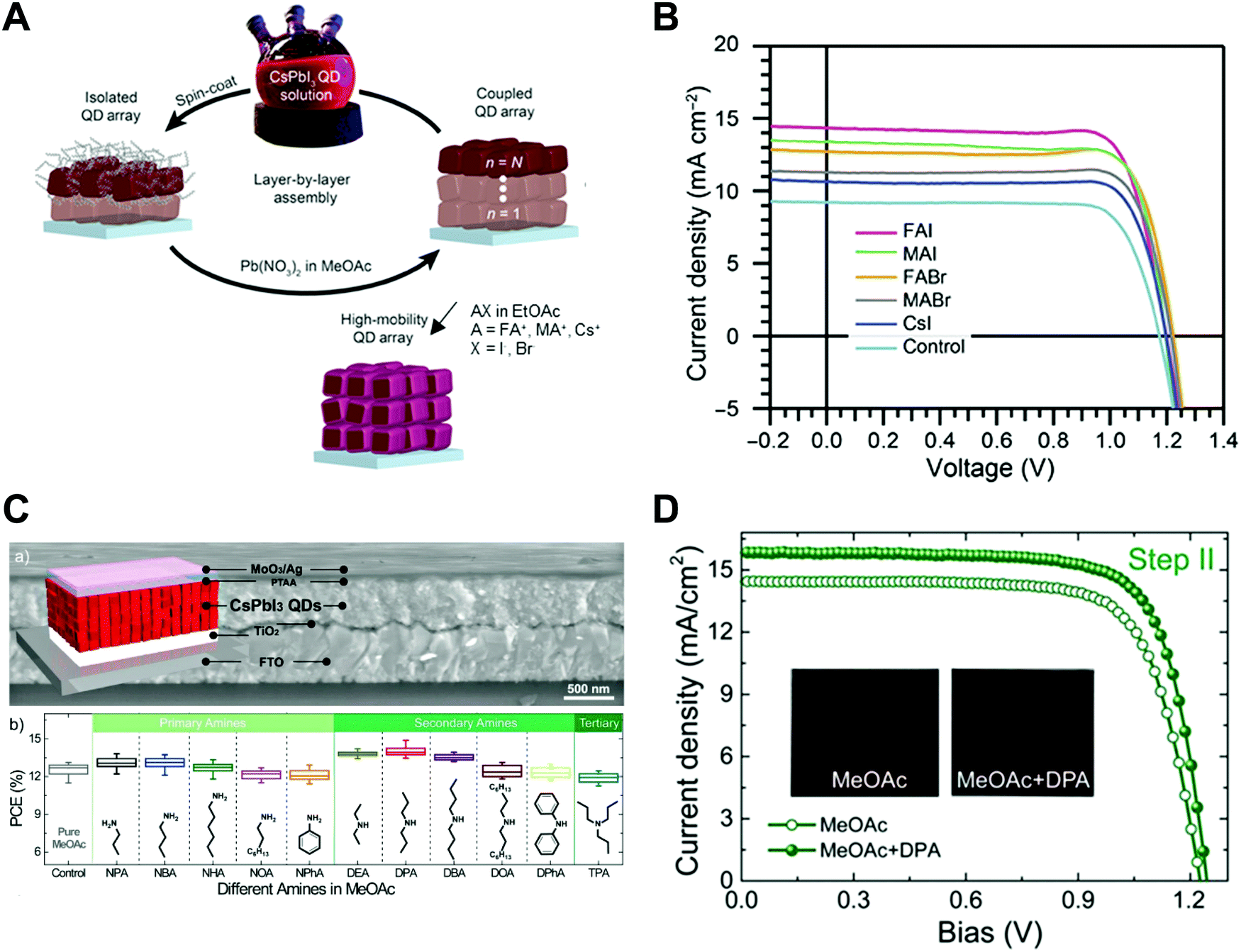 | ||
| Fig. 22 PV applications based on spin-assisted LbL assembly of perovskites nano-colloids. (A) Schematic illustration of CsPbI3 composite preparation process and AX salts post-treatment. (B) J–V curves of CsPbI3 composite based devices treated with FAI, methylammonium iodide (MAI), formamidinium bromide (FABr), methylammonium bromide (MABr), cesium iodide (CsI), and neat EtOAc control. Adapted from ref. 186 under the terms of the CC BY-NC, Creative Commons Attribution NonCommercial License 4.0 (https://creativecommons.org/licenses/by-nc/4.0), copyright 2017 AAAS. (C, top) Schematics and cross-sectional SEM image of the CsPbI3 nano-colloid assembled solar cell and (bottom) PCEs of CsPbI3 nano-colloid assembled solar cells depending on different post-treatment by various organic amines (see Fig. 10D). (D) J–V curves of CsPbI3 nano-colloid assembled solar cells treated by MeOAc w/wo DPA. Adapted from ref. 185 with permission from John Wiley and Sons, copyright 2020. | ||
6.4. Enhancement of optical and electronic properties by controlled composite states
Several examples of composites fabricated by LE-LbL assembly with optically and electronically active nano-colloids are described in this section. As explained above, LE-LbL assembly can provide an efficient way to fabricate various nano-colloidal composites with high-packing density, precise thickness control, desired multilayer structure, and favorable interfacial interactions in a controlled manner. Herein, we describe how the optical or electronic properties of nano-confined materials in LbL-assembled composite states can be enhanced according to the control of their structural parameters.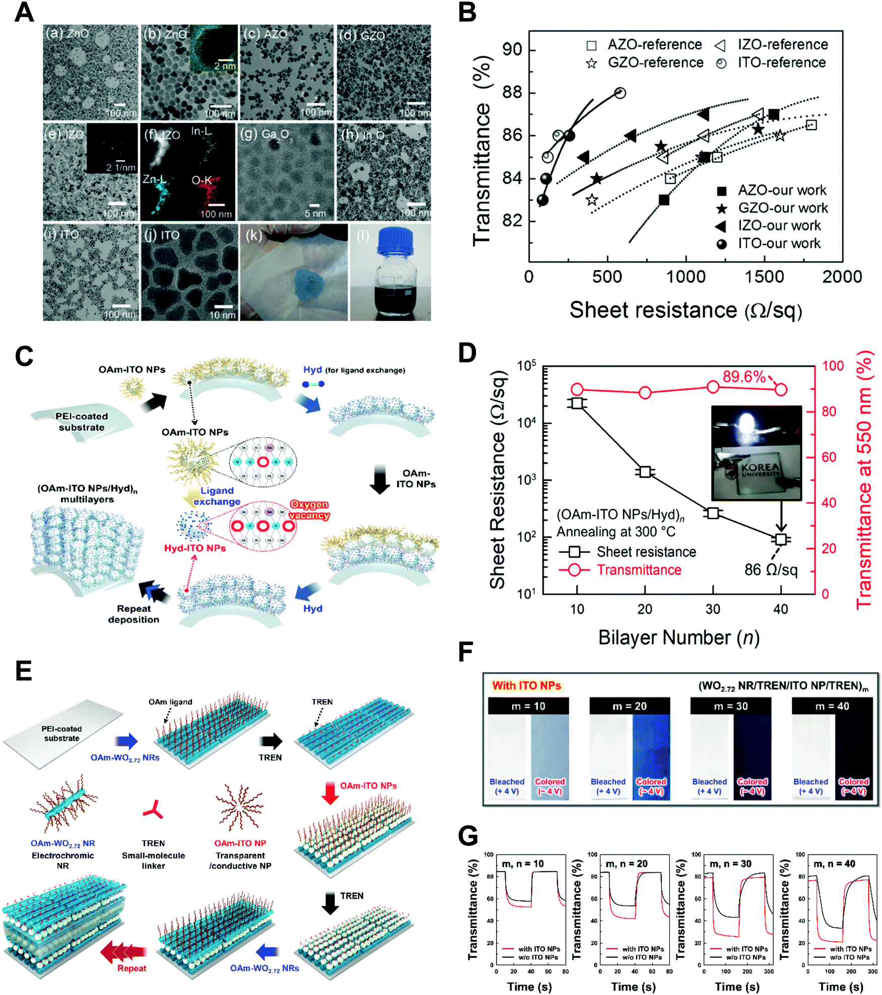 | ||
| Fig. 23 (A) TEM images of ZnO NPs, aluminum-doped ZnO (AZO) NPs, gallium-doped ZnO (GZO) NPs, indium-doped ZnO (IZO) NPs (the inset shows STEM image and elemental mappings of IZO NPs), Ga2O3 NPs, In2O3 NPs and ITO NPs (additionally, photographic images of powder of ITO NPs synthesized on a large scale and 30 mL of ITO NP ink after redispersion in toluene). (B) Integrated performances of transmittance and sheet resistance in this study (solid line), compared to the recently reported results (hollo: AZO, GZO, IZO, and ITO). Adapted from ref. 255 with permission from John Wiley and Sons, copyright 2014. (C) Schematic illustration of the preparation of ITO NP-based transparent conductive electrodes by NH2-functionalized hydrazine linker-induced LbL assembly. These hydrazine linkers with strong chemical reducing properties minimize the separation distance between adjacent ITO NPs by substituting bulky native ligands, and simultaneously, increase the level of oxygen vacancies within the ITO NPs. (D) Sheet resistance and optical transmittance at 550 nm of (OAm-ITO NPs/Hyd)n multilayers on quartz glasses after thermal annealing at 300 °C as a function of bilayer number (n). The inset shows a photograph of (OAm-ITO NPs/Hyd)40 multilayers on quartz glass connected with an LED. Adapted from ref. 263 with permission from John Wiley and Sons, copyright 2020. (E) Scheme for the formation of electrochromic nanocomposite films based on WO2.72 NRs and transparent/conductive ITO NPs by a LbL-assembly using small-molecule linkers. (F) Photographic images of (WO2.72 NR/TREN/ITO NP/TREN)m multilayers under applied potentials of +4.0 V (bleached state) and −4.0 V (colored state) as a function of periodic number (m). (G) Comparison of EC switching behaviors between WO2.72 NR-based EC films with ITO NPs and those without ITO NPs at the same number of WO2.72 NR layers. Adapted from ref. 266 with permission from Royal Society of Chemistry, copyright 2019. | ||
The Sun group reported that monodisperse 11 nm-sized ITO NCs could be synthesized by thermal decomposition of indium acetylacetonate and tin bis(acetylacetonate)dichloride in octadecene containing OAm and OA stabilizers.260 Additionally, to increase the amount of oxygen deficiencies within pristine ITO NCs, spin-coated ITO NC assemblies were thermally annealed at 300 °C for 6 h under Ar and 5% H2 gases. Generally, it is well known that the presence of oxygen deficiencies within oxide materials can act as n-type dopants, transforming an insulating oxide into an electrically conductive oxide.261–263 However, despite this thermal annealing process, the formed ITO NC assemblies exhibited a relatively high sheet resistance of 356 Ω sq−1 (optical transparency ∼93% at a wavelength of 550 nm), which was inferior to that (sheet resistance <30 Ω sq−1) of commercial ITO glass. Although a higher thermal annealing process (>400 °C) can induce a lower sheet resistance of the ITO NC assemblies, their optical transparency can be notably decreased due to the carbonization of the residual organic ligands with long alkyl chains, resulting in strong light absorption.264 Therefore, effective removal of residual organic ligands without thermal treatment is critical for resolving this troublesome trade-off between electrical conductivity and optical transparency.
Although Fafarman et al. reported that bulky organic ligands could be removed from NCs through chemical treatment using ammonium thiocyanate, the reported approach could destabilize the NC films assembled onto the substrate.265 As an alternative, Cho et al. reported that extremely small hydrazine molecules composed of only two amine groups without carbon atoms could be LbL-assembled with OAm-ITO NCs through a consecutive ligand exchange reaction between hydrazine and native OAm ligands, which could allow the preparation of robust ITO NP films (Fig. 23C).263 They also demonstrated that hydrazine molecules could significantly increase the amount of oxygen deficiencies within ITO NCs due to their strong chemical reducing property during simple LbL deposition and could furthermore effectively prevent the carbonization-induced light absorption arising from high thermal annealing. As a result, the (OAm-ITO NC/hydrazine)40 film annealed at 300 °C exhibited a low sheet resistance of 86 Ω sq−1 and a high optical transmittance of ∼89.6% (at a wavelength of 550 nm) (Fig. 23D).
This approach using small organic linkers and ligand exchange reactions can be further applied to various other optoelectronic films as well as transparent conductive films. Yun et al. also reported that LbL-assembled films composed of OAm-WO2.72 nanorod (OAm-WO2.72 NR), TREN, and OAm-ITO NCs could exhibit high-performance electrochromic properties with high color contrast (i.e., optical modulation), fast switching times (i.e., coloration/bleaching times), and high coloration efficiencies (Fig. 23E–G).266 Considering that the electrochromic mechanism of WOx in a lithium electrolyte is based on the reversible insertion/extraction of Li+ ions and electrons under applied potentials, the poor electrical conductivity of WO2.72 as well as the bulky OAm ligands onto WO2.72 nanorods caused sluggish charge transfer, resulting in low electrochromic performance. However, they demonstrated that the ligand exchange reaction using TREN molecule linkers and periodic incorporation of conductive ITO NCs into WO2.72-based films could significantly improve the charge transfer within the multilayers and resultantly realize much higher electrochromic performance than that of ITO NP-free WO2.72 or polymer linker-based WO2.72 films (Fig. 23F and G). These phenomena evidently show that effective interface control between neighboring active nanomaterials has a critical impact on the charge transfer within and corresponding performance of transparent/conductive NC films.
Recently, Cho and coworkers reported that OA-QDs (i.e., CdSe core–CdS shell, shortly CdSe@CdS nano-colloids) could be chemically deposited onto an NH2-functionalized poly(amidoamine) dendrimer (PAD)-coated electron transport layer (i.e., a ZnO ETL) through a ligand exchange reaction between OA ligands and NH2 groups of PAD, and additionally these PAD ligands could control the electron injection rate from the ETL into QDs by partially changing the electronic levels of the ZnO surface (Fig. 24A).274 Consistent with these phenomena, the resultant device efficiency (particularly the maximum EQE) was dramatically increased from 3.86 to 11.36% when the native OA ligands were replaced by PAD linkers (specifically, PAD with generation 3 or PAD-G3) (Fig. 24B). Furthermore, they demonstrated that ligand-asymmetric QDs composed of hydrophilic bottom ligands (i.e., NH2-PAD-G3) and hydrophobic top ligands (i.e., dodecylamine, DA) could be sandwiched between a hydrophilic ETL and a hydrophobic hole transporting layer (HTL), which could have a significant effect on the device performance (Fig. 24C–E).275 Specifically, the bottom ligands of the QDs in contact with the ZnO ETL operated as an effective electron blocking layer, and on the other hand the top ligands induced uniform deposition of the HTL (i.e., 1,3-bis(N-carbazolyl)benzene (mCP)) with an enhanced hole injection property. That is, because of the suppressed electron overflow (by the bottom ligand/ETL pair) and the stimulated hole injection (by the top ligand/HTL pair), the balance of charge injection in the QDs was synergistically increased. As a result, the EQE of the ligand-asymmetric QD-based device (i.e., the DA (top ligand)/QD/PAD (bottom ligand)-structured device) was significantly enhanced compared to those of other devices (i.e., OA/QD/OA- or OA/QD/PAD-structured devices) (Fig. 24D and E). These results evidently imply that ligand-controlled nano-confinement of QDs plays a pivotal role in determining their optoelectronic properties.
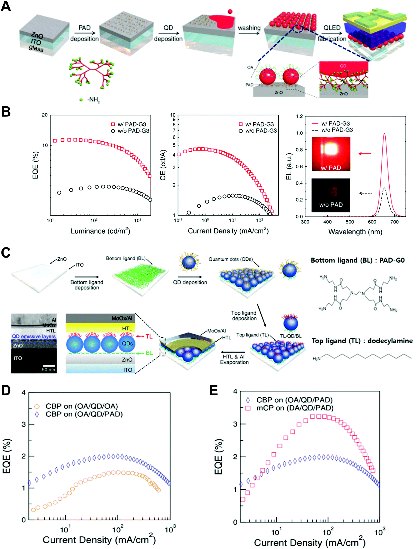 | ||
| Fig. 24 (A) Schematic illustration of ligand exchange process, PAD ligand, and interface between QDs and ZnO layer. (B) External quantum efficiency (EQE) vs. luminance (left data), current efficiency (CE) vs. luminance (middle data), and electroluminescence (EL) spectra (at a current density of 10 mA cm−2) and photographs (the inset) of QLEDs with native ligands (w/o PAD-G3, black) and dendrimer ligands (w/PAD-G3) (right data). Adapted from ref. 274 with permission from American Chemical Society, copyright 2017. (C) Scheme for fabrication process for blue QLED incorporating ligand-asymmetric Janus QDs and its cross-sectional transmission electron microscopy (TEM) image (left image). Chemical structures of bottom ligand (PAD-G0) and top ligand (dodecylamine) (right image). (D) External quantum efficiency (EQE) vs. current density of QLEDs with CBP on (OA/QD/OA) and (OA/QD/PAD). (E) EQE vs. current density of QLEDs with CBP on (OA/QD/PAD) and mCP on (DA/QD/PAD). Adapted from ref. 275 with permission from American Chemical Society, copyright 2018. | ||
7. Challenges and perspectives
In this review, we systematically discussed how confinement features could affect the electronic properties of optoelectronic materials based on conjugated polymers and perovskites. We also demonstrated that nano-confined optoelectronic materials could exhibit a high degree of morphological control through different confinement geometries (from 1D to 3D geometries), showing remarkable electronic properties and device performance. Despite significant advances in this field, high-performance optoelectronic devices that can outperform the devices prepared by conventional approaches are still lacking. We discuss several significant challenges and perspectives for each confinement geometry for further advancement in this field.1D nano-confinement
To enhance the controllability of the nano-morphology of optoelectronic materials under 1D nano-confinement, it is desirable that specific methods such as directional force-assisted control should be further considered. That is, the directional force occurring during deposition of optoelectronic materials can contribute to the control of their crystallization behavior, in addition to the nano-confinement-induced finite size and interfacial effects. For example, the push coating method (by Ikawa et al.) and the soft-cover method (by Ye et al.) use the moving meniscus at the edges of the cover layer during the peeling-off procedures to impose directional forces. Although these methods could show better controllability of organic and inorganic optoelectronic materials, the additional contribution of directional forces to the resultant morphology has not yet been exactly identified and fully understood. Therefore, systematic studies on the additional effects of directional forces by varying the directions and speed of the forces applied to solutions are highly required for the framework of nano-confinement principles.2D nano-confinement
Significant advances in nanofabrication methods have also been achieved for 2D nano-confinement. Structural templates can be easily removed from 2D nano-confined materials under mild conditions with the aid of a pattern-transfer method with flexible molds, which is very effective for preparing vertical-standing nanopillar or nanograting structures. However, despite this effectiveness, 2D nano-confined materials have much difficulty in being directly applied to actual devices without in-depth consideration of complementary interactions between vertically coated heterogeneous materials (e.g., metal electrode/optoelectronic materials or charge-transporting layer/optoelectronic material layer). For example, when the optoelectronic active layer is sandwiched between top and bottom electrodes or between the charge transporting layer and an electrode, unfavorable interactions at the heterogeneous interfaces has a poor effect on the charge extraction/injection that is closely related to the device performance. Therefore, the preparation of high-performance optoelectronic devices requires a fabrication approach that could deposit heterogeneous materials without disturbing the coating qualities of underlying active materials. Moreover, detailed characterization and analysis are required to elucidate the structure-dependent electronic properties of nano-confined optoelectronic materials. It should be noted that there have been only a few reports characterizing the electronic properties of 2D nano-confined materials (see Tables 2 and 3), and nanoscale characterization has rarely been performed on 2D nano-confined systems. SFM technology with various operation modes can provide a facile characterization tool for effectively understanding the structure–electronic property relationships induced by nano-confinement.3D nano-confinement
As a 3D nano-confinement system, the assembly of nano-colloids shows distinctive collective properties, depending on the structural parameters, that are different from those of the bulk state. In contrast to conventional deposition methods for nano-colloidal assembly, LE-LbL assembly can allow the deposition of nano-colloids with controllable packing density. Furthermore, LbL-assembled nano-colloids (e.g., Au, ITO, WOx, CdSe nano-colloids) can exhibit the structural parameter (i.e., packing density in lateral and vertical dimension)-dependent optical and electronic properties. Further studies on perovskites nano-colloids with controlled chemical compositions are expected to provide a new avenue for developing nano-confinement-based optoelectronic applications.Despite considerable progress in the assembly approaches for 1D, 2D, and 3D nano-confinement, there has been still a lack of fundamental understanding of nano-morphology formation process of optoelectronic materials under nano-confinement. As a consequence, further experimental and theoretical studies should be performed to elucidate mechanism and prediction models for nano-confined self-assembly of optoelectronic materials. To this end, in situ and in operando characterization methods are required for exploring the kinetic process of the self-assembly in real time. Among various methods suggested, in situ grazing incidence small/wide-angle X-ray scattering (i.e., GISAXS and GIWAXS) is one of the best known methods, which enables the investigation of nanostructure ranging from sub-nm to 100 nm with fast time resolution (<1 s). Particularly, morphology evolution124,277–283 and degradation process284–291 of organic and inorganic optoelectronic materials have been intensively investigated by using in situ GISAXS and GIWAXS methods. These characterization techniques and analysis methods can be effectively employed to investigate the kinetics of nano-confined self-assembly of optoelectronic materials.
In addition to in situ kinetic investigations, theories and computational simulations are required in order to capture further insight into nano-confined assembly process as well as to develop their prediction models. Several different types of theories and simulation methods can be employed for this purpose. For instance, Monte Carlo simulation,292 self-consistent field theory,293 dynamical density functional simulations,294 and simulated annealing method on a lattice model295,296 have been successfully used to predict the unusual self-assembly behavior of block copolymers under nano-confinement. Specifically, these modeling methods have allowed for predicting the shape, size and orientation of nanodomains of nano-confined block copolymers, which can also be effectively used for predicting the nano-confined self-assembly behavior of optoelectronic materials. Furthermore, an effective combination of experimental, theoretical, and simulation studies will provide important insights for fundamentally understanding the nano-confined self-assembly behavior of optoelectronic materials.
In this review, we demonstrate that nano-confined self-assembly/crystallization of optoelectronic materials is a rational and predictive approach to induce the formation of favorable morphology/crystallinity of materials, and furthermore enhance their electronic properties. However, for better advanced next-generation optoelectronic devices through the effective nano-confinement of optoelectronic materials, the development of more ingenious and novel solution process is highly desired, which, in turn, also contributes to addressing significant challenges associated with the empirical optimization of conventional approaches. Moreover, if this nano-confinement approach addressed in this review can be further expanded to other functional materials (i.e., metal–organic frameworks, metal oxides, ionic liquids, and biomolecules), we believe that it can also prompt a basis for developing and designing a variety of applications related to catalysis, photonics, bioelectronics and electrochemistry.
Conflicts of interest
The authors declare no conflict of interest.Acknowledgements
This work was supported by the National Research Foundation of Korea (NRF) grant funded by the Korea government (MSIT; Ministry of Science and ICT) (2019R1A4A1027627; 2020R1A2C1011571; 2010-0018290). We acknowledged the support of Alexander Klasen (MPI-P) and we thank the International Research Training Group 1404 ‘Self-organized Materials for Optoelectronics’ (DFG) for their financial support.References
- J. H. Burroughes, D. D. C. Bradley, A. R. Brown, R. N. Marks, K. Mackay, R. H. Friend, P. L. Burns and A. B. Holmes, Nature, 1990, 347, 539–541 CrossRef CAS.
- J. J. M. Halls, C. A. Walsh, N. C. Greenham, E. A. Marseglia, R. H. Friend, S. C. Moratti and A. B. Holmes, Nature, 1995, 376, 498–500 CrossRef CAS.
- G. Yu, J. Gao, J. C. Hummelen, F. Wudl and A. J. Heeger, Science, 1995, 270, 1789–1791 CrossRef CAS.
- S. R. Forrest, Nature, 2004, 428, 911–918 CrossRef CAS PubMed.
- M. M. Lee, J. Teuscher, T. Miyasaka, T. N. Murakami and H. J. Snaith, Science, 2012, 338, 643–647 CrossRef CAS PubMed.
- L. Dou, Y. M. Yang, J. You, Z. Hong, W.-H. Chang, G. Li and Y. Yang, Nat. Commun., 2014, 5, 1–6 Search PubMed.
- Z.-K. Tan, R. S. Moghaddam, M. L. Lai, P. Docampo, R. Higler, F. Deschler, M. Price, A. Sadhanala, L. M. Pazos, D. Credgington, F. Hanusch, T. Bein, H. J. Snaith and R. H. Friend, Nat. Nanotechnol., 2014, 9, 687–692 CrossRef CAS PubMed.
- H. Lee, C. Park, D. H. Sin, J. H. Park and K. Cho, Adv. Mater., 2018, 30, 1800453 CrossRef PubMed.
- F. Zhao, C. Wang and X. Zhan, Adv. Energy Mater., 2018, 8, 1703147 CrossRef.
- Y. Li, L. Ji, R. Liu, C. Zhang, C. H. Mak, X. Zou, H.-H. Shen, S.-Y. Leu and H.-Y. Hsu, J. Mater. Chem. A, 2018, 6, 12842–12875 RSC.
- H. Choi, K. Choi, Y. Choi, T. Kim, S. Lim and T. Park, Small Methods, 2020, 4, 1900569 CrossRef CAS.
- N. K. Tailor, M. Abdi-Jalebi, V. Gupta, H. Hu, M. I. Dar, G. Li and S. Satapathi, J. Mater. Chem. A, 2020, 8, 21356–21386 RSC.
- L. Zeng, S. Chen, K. Forberich, C. J. Brabec, Y. Mai and F. Guo, Energy Environ. Sci., 2020, 13, 4666–4690 RSC.
- R. M. Michell, I. Blaszczyk-Lezak, C. Mijangos and A. J. Müller, J. Polym. Sci., Part B: Polym. Phys., 2014, 52, 1179–1194 CrossRef CAS.
- R. M. Michell and A. J. Mueller, Prog. Polym. Sci., 2016, 54, 183–213 CrossRef.
- S. Napolitano, E. Glynos and N. B. Tito, Rep. Prog. Phys., 2017, 80, 036602 CrossRef PubMed.
- F. C. Meldrum and C. O'Shaughnessy, Adv. Mater., 2020, 32, 2001068 CrossRef CAS PubMed.
- S. D. Stranks, G. E. Eperon, G. Grancini, C. Menelaou, M. J. P. Alcocer, T. Leijtens, L. M. Herz, A. Petrozza and H. J. Snaith, Science, 2013, 342, 341–344 CrossRef CAS PubMed.
- S. De Wolf, J. Holovsky, S.-J. Moon, P. Löper, B. Niesen, M. Ledinsky, F.-J. Haug, J.-H. Yum and C. Ballif, J. Phys. Chem. Lett., 2014, 5, 1035–1039 CrossRef CAS PubMed.
- G. E. Eperon, S. D. Stranks, C. Menelaou, M. B. Johnston, L. M. Herz and H. J. Snaith, Energy Environ. Sci., 2014, 7, 982–988 RSC.
- M. Aryal, K. Trivedi and W. Hu, ACS Nano, 2009, 3, 3085–3090 CrossRef CAS PubMed.
- J. S. Kim, Y. Park, D. Y. Lee, J. H. Lee, J. H. Park, J. K. Kim and K. Cho, Adv. Funct. Mater., 2010, 20, 540–545 CrossRef CAS.
- H. Hlaing, X. Lu, T. Hofmann, K. G. Yager, C. T. Black and B. M. Ocko, ACS Nano, 2011, 5, 7532–7538 CrossRef CAS PubMed.
- Y.-X. Chen, Q.-Q. Ge, Y. Shi, J. Liu, D.-J. Xue, J.-Y. Ma, J. Ding, H.-J. Yan, J.-S. Hu and L.-J. Wan, J. Am. Chem. Soc., 2016, 138, 16196–16199 CrossRef CAS PubMed.
- S. Ma, S. H. Kim, B. Jeong, H. C. Kwon, S. C. Yun, G. Jang, H. Yang, C. Park, D. Lee and J. Moon, Small, 2019, 15, 1900219 CrossRef PubMed.
- A. Swarnkar, A. R. Marshall, E. M. Sanehira, B. D. Chernomordik, D. T. Moore, J. A. Christians, T. Chakrabarti and J. M. Luther, Science, 2016, 354, 92–95 CrossRef CAS PubMed.
- M. Ramanathan, I. S. Michael Kilbey, Q. Ji, J. P. Hill and K. Ariga, J. Mater. Chem., 2012, 22, 10389–10405 RSC.
- D. Gentili, F. Valle, C. Albonetti, F. Liscio and M. Cavallini, Acc. Chem. Res., 2014, 47, 2692–2699 CrossRef CAS PubMed.
- X. Kong, K. Zong and S. S. Lee, Chem. Mater., 2019, 31, 4953–4970 CrossRef CAS.
- Z. Bao, A. Dodabalapur and A. J. Lovinger, Appl. Phys. Lett., 1996, 69, 4108–4110 CrossRef CAS.
- H. Sirringhaus, N. Tessler and R. H. Friend, Science, 1998, 280, 1741–1744 CrossRef CAS PubMed.
- H. Sirringhaus, P. J. Brown, R. H. Friend, M. M. Nielsen, K. Bechgaard, B. M. W. Langeveld-Voss, A. J. H. Spiering, R. A. J. Janssen, E. W. Meijer, P. Herwig and D. M. de Leeuw, Nature, 1999, 401, 685–688 CrossRef CAS.
- P. Schilinsky, C. Waldauf and C. J. Brabec, Appl. Phys. Lett., 2002, 81, 3885–3887 CrossRef CAS.
- Y. Li and Y. Zou, Adv. Mater., 2008, 20, 2952–2958 CrossRef CAS.
- J.-S. Kim, J.-H. Kim, W. Lee, H. Yu, H. J. Kim, I. Song, M. Shin, J. H. Oh, U. Jeong, T.-S. Kim and B. J. Kim, Macromolecules, 2015, 48, 4339–4346 CrossRef CAS.
- H. Park, B. S. Ma, J.-S. Kim, Y. Kim, H. J. Kim, D. Kim, H. Yun, J. Han, F. S. Kim, T.-S. Kim and B. J. Kim, Macromolecules, 2019, 52, 7721–7730 CrossRef CAS.
- N. Blouin, A. Michaud and M. Leclerc, Adv. Mater., 2007, 19, 2295–2300 CrossRef CAS.
- S. H. Park, A. Roy, S. Beaupre, S. Cho, N. Coates, J. S. Moon, D. Moses, M. Leclerc, K. Lee and A. J. Heeger, Nat. Photonics, 2009, 3, 297–302 CrossRef CAS.
- Y. Liang, Z. Xu, J. Xia, S. T. Tsai, Y. Wu, G. Li, C. Ray and L. Yu, Adv. Mater., 2010, 22, E135–E138 CrossRef CAS PubMed.
- Z. He, C. Zhong, S. Su, M. Xu, H. Wu and Y. Cao, Nat. Photonics, 2012, 6, 591–595 CrossRef.
- L. Dou, Y. Liu, Z. Hong, G. Li and Y. Yang, Chem. Rev., 2015, 115, 12633–12665 CrossRef CAS PubMed.
- Z. He, B. Xiao, F. Liu, H. Wu, Y. Yang, S. Xiao, C. Wang, T. P. Russell and Y. Cao, Nat. Photonics, 2015, 9, 174–179 CrossRef CAS.
- M. Kim, S. U. Ryu, S. A. Park, K. Choi, T. Kim, D. Chung and T. Park, Adv. Funct. Mater., 2020, 30, 1904545 CrossRef CAS.
- Q. Dong, Y. Fang, Y. Shao, P. Mulligan, J. Qiu, L. Cao and J. Huang, Science, 2015, 347, 967–970 CrossRef CAS.
- X. D. Wang, W. G. Li, J. F. Liao and D. B. Kuang, Solar RRL, 2019, 3, 1800294 CrossRef.
- Y. Liu, Y. Zhang, Z. Yang, D. Yang, X. Ren, L. Pang and S. Liu, Adv. Mater., 2016, 28, 9204–9209 CrossRef CAS PubMed.
- H.-S. Rao, B.-X. Chen, X.-D. Wang, D.-B. Kuang and C.-Y. Su, Chem. Commun., 2017, 53, 5163–5166 RSC.
- J. Peet, J. Y. Kim, N. E. Coates, W. L. Ma, D. Moses, A. J. Heeger and G. C. Bazan, Nat. Mater., 2007, 6, 497–500 CrossRef CAS PubMed.
- G. Wang, N. Persson, P.-H. Chu, N. Kleinhenz, B. Fu, M. Chang, N. Deb, Y. Mao, H. Wang, M. A. Grover and E. Reichmanis, ACS Nano, 2015, 9, 8220–8230 CrossRef CAS PubMed.
- P.-H. Chu, N. Kleinhenz, N. Persson, M. McBride, J. L. Hernandez, B. Fu, G. Zhang and E. Reichmanis, Chem. Mater., 2016, 28, 9099–9109 CrossRef CAS.
- N. Kleinhenz, N. Persson, Z. Xue, P. H. Chu, G. Wang, Z. Yuan, M. A. McBride, D. Choi, M. A. Grover and E. Reichmanis, Chem. Mater., 2016, 28, 3905–3913 CrossRef CAS.
- J. Y. Na, B. Kang, S. G. Lee, K. Cho and Y. D. Park, ACS Appl. Mater. Interfaces, 2017, 9, 9871–9879 CrossRef CAS PubMed.
- F. Padinger, R. S. Rittberger and N. S. Sariciftci, Adv. Funct. Mater., 2003, 13, 85–88 CrossRef CAS.
- G. Li, Y. Yao, H. Yang, V. Shrotriya, G. Yang and Y. Yang, Adv. Funct. Mater., 2007, 17, 1636–1644 CrossRef CAS.
- Y. Diao, Y. Zhou, T. Kurosawa, L. Shaw, C. Wang, S. Park, Y. Guo, J. A. Reinspach, K. Gu, X. Gu, B. C. K. Tee, C. Pang, H. Yan, D. Zhao, M. F. Toney, S. C. B. Mannsfeld and Z. Bao, Nat. Commun., 2015, 6, 1–10 Search PubMed.
- X. Gu, L. Shaw, K. Gu, M. F. Toney and Z. Bao, Nat. Commun., 2018, 9, 1–16 CrossRef PubMed.
- S. Agbolaghi and S. Zenoozi, Org. Electron., 2017, 51, 362–403 CrossRef CAS.
- J. W. Lee, D. K. Lee, D. N. Jeong and N. G. Park, Adv. Funct. Mater., 2019, 29, 1807047 CrossRef CAS.
- J. A. Aguiar, S. Wozny, T. G. Holesinger, T. Aoki, M. K. Patel, M. Yang, J. J. Berry, M. Al-Jassim, W. Zhou and K. Zhu, Energy Environ. Sci., 2016, 9, 2372–2382 RSC.
- J. Cao, X. Jing, J. Yan, C. Hu, R. Chen, J. Yin, J. Li and N. Zheng, J. Am. Chem. Soc., 2016, 138, 9919–9926 CrossRef CAS PubMed.
- N. J. Jeon, J. H. Noh, W. S. Yang, Y. C. Kim, S. Ryu, J. Seo and S. I. Seok, Nature, 2015, 517, 476–480 CrossRef CAS PubMed.
- W. Nie, H. Tsai, R. Asadpour, J.-C. Blancon, A. J. Neukirch, G. Gupta, J. J. Crochet, M. Chhowalla, S. Tretiak and M. A. Alam, Science, 2015, 347, 522–525 CrossRef CAS PubMed.
- N. J. Jeon, J. H. Noh, Y. C. Kim, W. S. Yang, S. Ryu and S. I. Seok, Nat. Mater., 2014, 13, 897–903 CrossRef CAS PubMed.
- A. Dualeh, N. Tétreault, T. Moehl, P. Gao, M. K. Nazeeruddin and M. Grätzel, Adv. Funct. Mater., 2014, 24, 3250–3258 CrossRef CAS.
- Z. Xiao, Q. Dong, C. Bi, Y. Shao, Y. Yuan and J. Huang, Adv. Mater., 2014, 26, 6503–6509 CrossRef CAS PubMed.
- N. Ahn, D.-Y. Son, I.-H. Jang, S. M. Kang, M. Choi and N.-G. Park, J. Am. Chem. Soc., 2015, 137, 8696–8699 CrossRef CAS PubMed.
- J. Burschka, N. Pellet, S.-J. Moon, R. Humphry-Baker, P. Gao, M. K. Nazeeruddin and M. Grätzel, Nature, 2013, 499, 316–319 CrossRef CAS PubMed.
- J.-H. Im, H.-S. Kim and N.-G. Park, APL Mater., 2014, 2, 081510 CrossRef.
- E. Beniash, J. Aizenberg, L. Addadi and S. Weiner, Proc. R. Soc. B, 1997, 264, 461–465 CrossRef CAS.
- M. Beiner, G. T. Rengarajan, S. Pankaj, D. Enke and M. Steinhart, Nano Lett., 2007, 7, 1381–1385 CrossRef CAS PubMed.
- T. Giesa and M. J. Buehler, Annu. Rev. Biophys., 2013, 42, 651–673 CrossRef CAS PubMed.
- Y. Liu, J. Goebl and Y. Yin, Chem. Soc. Rev., 2013, 42, 2610–2653 RSC.
- H. Ping, H. Xie and Z. Fu, J. Materiomics, 2017, 3, 83–95 CrossRef.
- B. D. Hamilton, J.-M. Ha, M. A. Hillmyer and M. D. Ward, Acc. Chem. Res., 2012, 45, 414–423 CrossRef CAS.
- Q. Jiang and M. D. Ward, Chem. Soc. Rev., 2014, 43, 2066–2079 RSC.
- G. Reiter, Europhys. Lett., 1993, 23, 579 CrossRef CAS.
- P. G. de Gennes, Macromolecules, 1980, 13, 1069–1075 CrossRef CAS.
- P. K. Brazhnik, K. F. Freed and H. Tang, J. Chem. Phys., 1994, 101, 9143–9154 CrossRef CAS.
- C. J. Ellison and J. M. Torkelson, Nat. Mater., 2003, 2, 695–700 CrossRef CAS PubMed.
- C. B. Roth, K. L. McNerny, W. F. Jager and J. M. Torkelson, Macromolecules, 2007, 40, 2568–2574 CrossRef CAS.
- M. Tesfaye, D. I. Kushner, B. D. McCloskey, A. Z. Weber and A. Kusoglu, ACS Macro Lett., 2018, 7, 1237–1242 CrossRef CAS.
- H. Wang, J. K. Keum, A. Hiltner and E. Baer, Macromolecules, 2009, 42, 7055–7066 CrossRef CAS.
- H. Wang, J. K. Keum, A. Hiltner and E. Baer, Macromolecules, 2010, 43, 3359–3364 CrossRef CAS.
- J. M. Carr, D. S. Langhe, M. T. Ponting, A. Hiltner and E. Baer, J. Mater. Res., 2012, 27, 1326 CrossRef CAS.
- C. M. Stafford, B. D. Vogt, C. Harrison, D. Julthongpiput and R. Huang, Macromolecules, 2006, 39, 5095–5099 CrossRef CAS.
- X. Cheng, K. W. Putz, C. D. Wood and L. C. Brinson, Macromol. Rapid Commun., 2015, 36, 391–397 CrossRef CAS PubMed.
- M.-C. Ma and Y.-L. Guo, Chin. J. Polym. Sci., 2020, 38, 565–578 CrossRef CAS.
- H. Schönherr and C. W. Frank, Macromolecules, 2003, 36, 1199–1208 CrossRef.
- E. Woo, J. Huh, Y. G. Jeong and K. Shin, Phys. Rev. Lett., 2007, 98, 136103 CrossRef PubMed.
- Y. Guan, G. Liu, P. Gao, L. Li, G. Ding and D. Wang, ACS Macro Lett., 2013, 2, 181–184 CrossRef CAS.
- L. Li, K. Matsunaga, J. Zhu, T. Higuchi, H. Yabu, M. Shimomura, H. Jinnai, R. C. Hayward and T. P. Russell, Macromolecules, 2010, 43, 7807–7812 CrossRef CAS.
- Z. Jin and H. Fan, Soft Matter, 2014, 10, 9212–9219 RSC.
- H. Yabu, T. Higuchi and H. Jinnai, Soft Matter, 2014, 10, 2919–2931 RSC.
- K. H. Ku, J. M. Shin, H. Yun, G. R. Yi, S. G. Jang and B. Kim, Adv. Funct. Mater., 2018, 28, 1802961 CrossRef.
- J. J. Shin, E. J. Kim, K. H. Ku, Y. J. Lee, C. J. Hawker and B. J. Kim, ACS Macro Lett., 2020, 9, 306–317 CrossRef CAS.
- Z. Zhang, D. Gekhtman, M. S. Dresselhaus and J. Y. Ying, Chem. Mater., 1999, 11, 1659–1665 CrossRef CAS.
- C. Anduix-Canto, Y.-Y. Kim, Y.-W. Wang, A. Kulak, F. C. Meldrum and H. K. Christenson, Cryst. Growth Des., 2016, 16, 5403–5411 CrossRef CAS.
- B. Cantaert, E. Beniash and F. C. Meldrum, Chem. – Eur. J., 2013, 19, 14918–14924 CrossRef CAS PubMed.
- N. B. J. Hetherington, A. N. Kulak, Y. Y. Kim, E. H. Noel, D. Snoswell, M. Butler and F. C. Meldrum, Adv. Funct. Mater., 2011, 21, 948–954 CrossRef CAS.
- S. H. Tolbert and A. P. Alivisatos, Science, 1994, 265, 373–376 CrossRef CAS PubMed.
- A. P. Alivisatos, Science, 1996, 271, 933–937 CrossRef CAS.
- T. Castro, R. Reifenberger, E. Choi and R. P. Andres, Phys. Rev. B: Condens. Matter Mater. Phys., 1990, 42, 8548 CrossRef CAS PubMed.
- C. C. Yang and S. Li, J. Phys. Chem. C, 2008, 112, 16400–16404 CrossRef CAS.
- Y. Ko, C. H. Kwon, S. W. Lee and J. Cho, Adv. Mater., 2020, 32, 2001924 CrossRef CAS PubMed.
- J. Yang, Z. Zhao, S. Wang, Y. Guo and Y. Liu, Chem, 2018, 4, 2748–2785 CAS.
- K. Zhao, X. Yu, R. Li, A. Amassian and Y. Han, J. Mater. Chem. C, 2015, 3, 9842–9848 RSC.
- D. Kajiya and K.-i. Saitow, ACS Appl. Energy Mater., 2018, 1, 6881–6889 CrossRef CAS.
- H. Yan, Z. Chen, Y. Zheng, C. Newman, J. R. Quinn, F. Dötz, M. Kastler and A. Facchetti, Nature, 2009, 457, 679–686 CrossRef CAS PubMed.
- R. S. Jordan and Y. Wang, J. Polym. Sci., Part B: Polym. Phys., 2019, 57, 1592–1605 CrossRef CAS.
- M. Noebels, R. E. Cross, D. A. Evans and C. E. Finlayson, J. Mater. Sci., 2014, 49, 4279–4287 CrossRef CAS.
- H.-W. Hsu and C.-L. Liu, RSC Adv., 2014, 4, 30145–30149 RSC.
- L. H. Jimison, S. Himmelberger, D. T. Duong, J. Rivnay, M. F. Toney and A. Salleo, J. Polym. Sci., Part B: Polym. Phys., 2013, 51, 611–620 CrossRef CAS.
- B. X. Dong, J. K. Wenderott and P. F. Green, Colloid Polym. Sci., 2020 DOI:10.1007/s00396-020-04725-1.
- V. Skrypnychuk, N. Boulanger, V. Yu, M. Hilke, S. C. B. Mannsfeld, M. F. Toney and D. R. Barbero, Adv. Funct. Mater., 2015, 25, 664–670 CrossRef CAS.
- S. Chae, K. H. Cho, S. Won, A. Yi, J. Choi, H. H. Lee, J. H. Kim and H. J. Kim, Adv. Mater. Interfaces, 2017, 4, 1701099 CrossRef.
- H. Yang, E. Glynos, B. Huang and P. F. Green, J. Phys. Chem. C, 2013, 117, 9590–9597 CrossRef CAS.
- L. Janasz, D. Chlebosz, M. Gradzka, W. Zajaczkowski, T. Marszalek, K. Müllen, J. Ulanski, A. Kiersnowski and W. Pisula, J. Mater. Chem. C, 2016, 4, 11488–11498 RSC.
- L. Janasz, M. Gradzka, D. Chlebosz, W. Zajaczkowski, T. Marszalek, A. Kiersnowski, J. Ulanski and W. Pisula, Langmuir, 2017, 33, 4189–4197 CrossRef CAS PubMed.
- M. T. Dang, G. Wantz, H. Bejbouji, M. Urien, O. J. Dautel, L. Vignau and L. Hirsch, Sol. Energy Mater. Sol. Cells, 2011, 95, 3408–3418 CrossRef CAS.
- Z. Bao, A. Dodabalapur and A. Lovinger, Appl. Phys. Lett., 1996, 69, 4108–4110 CrossRef CAS.
- H. Yang, T. J. Shin, L. Yang, K. Cho, C. Y. Ryu and Z. Bao, Adv. Funct. Mater., 2005, 15, 671–676 CrossRef CAS.
- J.-F. Chang, B. Sun, D. W. Breiby, M. M. Nielsen, T. I. Sölling, M. Giles, I. McCulloch and H. Sirringhaus, Chem. Mater., 2004, 16, 4772–4776 CrossRef CAS.
- S. Guo, E. M. Herzig, A. Naumann, G. Tainter, J. Perlich and P. Müller-Buschbaum, J. Phys. Chem. B, 2014, 118, 344–350 CrossRef CAS.
- E. F. Manley, J. Strzalka, T. J. Fauvell, N. E. Jackson, M. J. Leonardi, N. D. Eastham, T. J. Marks and L. X. Chen, Adv. Mater., 2017, 29, 1703933 CrossRef PubMed.
- C. McDowell, M. Abdelsamie, M. F. Toney and G. C. Bazan, Adv. Mater., 2018, 30, 1707114 CrossRef PubMed.
- M. Ikawa, T. Yamada, H. Matsui, H. Minemawari, J. Y. Tsutsumi, Y. Horii, M. Chikamatsu, R. Azumi, R. Kumai and T. Hasegawa, Nat. Commun., 2012, 3, 1–8 Search PubMed.
- S. Kobayashi, D. Kaneto, S. Fujii, H. Kataura and Y. Nishioka, J. Chin. Adv. Mater. Soc., 2015, 3, 1–8 CrossRef CAS.
- V. Vohra, W. Mróz, S. Inaba, W. Porzio, U. Giovanella and F. Galeotti, ACS Appl. Mater. Interfaces, 2017, 9, 25434–25444 CrossRef CAS.
- F. Ye, H. Chen, F. Xie, W. Tang, M. Yin, J. He, E. Bi, Y. Wang, X. Yang and L. Han, Energy Environ. Sci., 2016, 9, 2295–2301 RSC.
- H. Chen, F. Ye, W. Tang, J. He, M. Yin, Y. Wang, F. Xie, E. Bi, X. Yang, M. Grätzel and L. Han, Nature, 2017, 550, 92–95 CrossRef CAS PubMed.
- F. Ye, W. Tang, F. Xie, M. Yin, J. He, Y. Wang, H. Chen, Y. Qiang, X. Yang and L. Han, Adv. Mater., 2017, 29, 1701440 CrossRef PubMed.
- Z. Chen, Q. Dong, Y. Liu, C. Bao, Y. Fang, Y. Lin, S. Tang, Q. Wang, X. Xiao, Y. Bai, Y. Deng and J. Huang, Nat. Commun., 2017, 8, 1–7 CrossRef.
- Y. Xia and G. M. Whitesides, Angew. Chem., Int. Ed., 1998, 37, 550–575 CrossRef CAS.
- D. Qin, Y. Xia and G. M. Whitesides, Nat. Protoc., 2010, 5, 491–502 CrossRef CAS PubMed.
- S. Y. Chou, P. R. Krauss and P. J. Renstrom, Science, 1996, 272, 85–87 CrossRef CAS.
- L. J. Guo, Adv. Mater., 2007, 19, 495–513 CrossRef CAS.
- K. Y. Suh, Y. S. Kim and H. H. Lee, Adv. Mater., 2001, 13, 1386–1389 CrossRef CAS.
- K. Y. Suh and H. H. Lee, Adv. Funct. Mater., 2002, 12, 405–413 CrossRef CAS.
- M. Cavallini, D. Gentili, P. Greco, F. Valle and F. Biscarini, Nat. Protoc., 2012, 7, 1668–1676 CrossRef CAS PubMed.
- D. Gentili, G. Foschi, F. Valle, M. Cavallini and F. Biscarini, Chem. Soc. Rev., 2012, 41, 4430–4443 RSC.
- X. Lu, H. Hlaing, C.-Y. Nam, K. G. Yager, C. T. Black and B. M. Ocko, Chem. Mater., 2015, 27, 60–66 CrossRef CAS.
- Y. Yang, K. Mielczarek, M. Aryal, A. Zakhidov and W. Hu, Nanoscale, 2014, 6, 7576–7584 RSC.
- V. Skrypnychuk, G. J. A. H. Wetzelaer, P. I. Gordiichuk, S. C. B. Mannsfeld, A. Herrmann, M. F. Toney and D. R. Barbero, Adv. Mater., 2016, 28, 2359–2366 CrossRef CAS.
- G. Ding, K. Wang, X. Li, C. Wang, Z. Hu and J. Liu, Polym. Chem., 2017, 8, 2666–2674 RSC.
- X. He, F. Gao, G. Tu, D. Hasko, S. Huttner, U. Steiner, N. C. Greenham, R. H. Friend and W. T. S. Huck, Nano Lett., 2010, 10, 1302–1307 CrossRef CAS PubMed.
- G. Ding, C. Li, X. Li, Y. Wu, J. Liu, Y. Li, Z. Hu and Y. Li, Nanoscale, 2015, 7, 11024–11032 RSC.
- D. E. Johnston, K. G. Yager, H. Hlaing, X. Lu, B. M. Ocko and C. T. Black, ACS Nano, 2014, 8, 243–249 CrossRef CAS PubMed.
- J. Ko, Y. Kim, J. S. Kang, R. Berger, H. Yoon and K. Char, Adv. Mater., 2020, 32, 1908087 CrossRef CAS PubMed.
- T. Kim, H. Yoon, H. J. Song, N. Haberkorn, Y. Cho, S. H. Sung, C. H. Lee, K. Char and P. Theato, Macromol. Rapid Commun., 2012, 33, 2035–2040 CrossRef CAS PubMed.
- S. Demchyshyn, J. M. Roemer, H. Groiß, H. Heilbrunner, C. Ulbricht, D. Apaydin, A. Böhm, U. Rütt, F. Bertram and G. Hesser, Sci. Adv., 2017, 3, e1700738 CrossRef PubMed.
- H. C. Kwon, A. Kim, H. Lee, D. Lee, S. Jeong and J. Moon, Adv. Energy Mater., 2016, 6, 1601055 CrossRef.
- D. Zhang, L. Gu, Q. Zhang, Y. Lin, D.-H. Lien, M. Kam, S. Poddar, E. C. Garnett, A. Javey and Z. Fan, Nano Lett., 2019, 19, 2850–2857 CrossRef CAS PubMed.
- D. H. Chun, Y. J. Choi, Y. In, J. K. Nam, Y. J. Choi, S. Yun, W. Kim, D. Choi, D. Kim and H. Shin, ACS Nano, 2018, 12, 8564–8571 CrossRef CAS PubMed.
- H. Wang, R. Haroldson, B. Balachandran, A. Zakhidov, S. Sohal, J. Y. Chan, A. Zakhidov and W. Hu, ACS Nano, 2016, 10, 10921–10928 CrossRef CAS.
- N. Pourdavoud, S. Wang, A. Mayer, T. Hu, Y. Chen, A. Marianovich, W. Kowalsky, R. Heiderhoff, H. C. Scheer and T. Riedl, Adv. Mater., 2017, 29, 1605003 CrossRef PubMed.
- B. Jeong, I. Hwang, S. H. Cho, E. H. Kim, S. Cha, J. Lee, H. S. Kang, S. M. Cho, H. Choi and C. Park, ACS Nano, 2016, 10, 9026–9035 CrossRef CAS PubMed.
- B. Jeong, H. Han, H. H. Kim, W. K. Choi, Y. J. Park and C. Park, ACS Nano, 2020, 14, 1645–1655 CrossRef CAS PubMed.
- G. Chen, J. Feng, H. Gao, Y. Zhao, Y. Pi, X. Jiang, Y. Wu and L. Jiang, Adv. Funct. Mater., 2019, 29, 1808741 CrossRef.
- J. Mao, W. E. Sha, H. Zhang, X. Ren, J. Zhuang, V. A. L. Roy, K. S. Wong and W. C. H. Choy, Adv. Funct. Mater., 2017, 27, 1606525 CrossRef.
- H.-C. Kim, S.-M. Park and W. D. Hinsberg, Chem. Rev., 2010, 110, 146–177 CrossRef CAS PubMed.
- C. M. Bates, M. J. Maher, D. W. Janes, C. J. Ellison and C. G. Willson, Macromolecules, 2014, 47, 2–12 CrossRef CAS.
- I. Botiz and S. B. Darling, Mater. Today, 2010, 13, 42–51 CrossRef CAS.
- J.-S. Kim, Y. J. Lee, J. P. Coote, G. E. Stein and B. J. Kim, Macromolecules, 2019, 52, 4475–4482 CrossRef CAS.
- X. Li, P. J. Wolanin, L. R. MacFarlane, R. L. Harniman, J. Qian, O. E. C. Gould, T. G. Dane, J. Rudin, M. J. Cryan, T. Schmaltz, H. Frauenrath, M. A. Winnik, C. F. J. Faul and I. Manners, Nat. Commun., 2017, 8, 1–9 CrossRef PubMed.
- L. Han, M. Wang, X. Jia, W. Chen, H. Qian and F. He, Nat. Commun., 2018, 9, 1–12 CrossRef CAS PubMed.
- J.-S. Kim, J.-E. Choi, H. Park, Y. Kim, H. J. Kim, J. Han, J. M. Shin and B. J. Kim, Polym. Chem., 2019, 10, 3030–3039 RSC.
- L. R. MacFarlane, H. Shaikh, J. D. Garcia-Hernandez, M. Vespa, T. Fukui and I. Manners, Nat. Rev. Mater., 2021, 6, 7–26 CrossRef CAS.
- A. M. M. Jani, D. Losic and N. H. Voelcker, Prog. Polym. Sci., 2013, 58, 636–704 Search PubMed.
- K. Wang, G. Liu, N. Hoivik, E. Johannessen and H. Jakobsen, Chem. Soc. Rev., 2014, 43, 1476–1500 RSC.
- Y. Zhang, C.-W. Lo, J. A. Taylor and S. Yang, Langmuir, 2006, 22, 8595–8601 CrossRef CAS PubMed.
- G. J. Slavik, G. Ragetly, N. Ganesh, D. J. Griffon and B. T. Cunningham, J. Mater. Chem., 2007, 17, 4095–4101 RSC.
- A. Carlson, A. M. Bowen, Y. Huang, R. G. Nuzzo and J. A. Rogers, Adv. Mater., 2012, 24, 5284–5318 CrossRef CAS PubMed.
- S.-J. Choi, H. N. Kim, W. G. Bae and K.-Y. Suh, J. Mater. Chem., 2011, 21, 14325–14335 RSC.
- S. H. Sung, H. Yoon, J. Lim and K. Char, Small, 2012, 8, 826–831 CrossRef CAS.
- K. G. Sharp, G. S. Blackman, N. J. Glassmaker, A. Jagota and C.-Y. Hui, Langmuir, 2004, 20, 6430–6438 CrossRef CAS PubMed.
- H. Yoon, S. H. Lee, S. H. Sung, K. Y. Suh and K. Char, Langmuir, 2011, 27, 7944–7948 CrossRef CAS PubMed.
- H. Yoon, T.-I. Kim, S. Choi, K. Y. Suh, M. J. Kim and H. H. Lee, Appl. Phys. Lett., 2006, 88, 254104 CrossRef.
- L. Letertre, R. Roche, O. Douhéret, H. G. Kassa, D. Mariolle, N. Chevalier, Ł. Borowik, P. Dumas, B. Grévin, R. Lazzaroni and P. Leclère, Beilstein J. Nanotechnol., 2018, 9, 2087–2096 CrossRef CAS PubMed.
- M. Wang, Y. Li, H. Huang, E. D. Peterson, W. Nie, W. Zhou, W. Zeng, W. Huang, G. Fang, N. Sun, X. Zhao and D. L. Carroll, Appl. Phys. Lett., 2011, 98, 55 Search PubMed.
- G. Tchutchulashvili, K. P. Korona, W. Mech, S. Chusnutdinow, M. Sobanska, K. Klosek, Z. R. Zytkiewicz and W. Sadowski, J. Nanopart. Res., 2020, 22, 1–9 CrossRef.
- G. E. Eperon, G. M. Paternò, R. J. Sutton, A. Zampetti, A. A. Haghighirad, F. Cacialli and H. J. Snaith, J. Mater. Chem. A, 2015, 3, 19688–19695 RSC.
- S. Dastidar, C. J. Hawley, A. D. Dillon, A. D. Gutierrez-Perez, J. E. Spanier and A. T. Fafarman, J. Phys. Chem. Lett., 2017, 8, 1278–1282 CrossRef CAS PubMed.
- L. Protesescu, S. Yakunin, M. I. Bodnarchuk, F. Krieg, R. Caputo, C. H. Hendon, R. X. Yang, A. Walsh and M. V. Kovalenko, Nano Lett., 2015, 15, 3692–3696 CrossRef CAS PubMed.
- X. Li, Y. Wu, S. Zhang, B. Cai, Y. Gu, J. Song and H. Zeng, Adv. Funct. Mater., 2016, 26, 2435–2445 CrossRef CAS.
- Y. Wang, J. Yuan, X. Zhang, X. Ling, B. W. Larson, Q. Zhao, Y. Yang, Y. Shi, J. M. Luther and W. Ma, Adv. Mater., 2020, 32, 2000449 CrossRef CAS PubMed.
- E. M. Sanehira, A. R. Marshall, J. A. Christians, S. P. Harvey, P. N. Ciesielski, L. M. Wheeler, P. Schulz, L. Y. Lin, M. C. Beard and J. M. Luther, Sci. Adv., 2017, 3, eaao4204 CrossRef PubMed.
- L. M. Wheeler, E. M. Sanehira, A. R. Marshall, P. Schulz, M. Suri, N. C. Anderson, J. A. Christians, D. Nordlund, D. Sokaras and T. Kroll, J. Am. Chem. Soc., 2018, 140, 10504–10513 CrossRef CAS PubMed.
- S. Shivarudraiah, M. Ng, C. A. Li and J. E. Halpert, ACS Appl. Energy Mater., 2020, 3, 5620–5627 CrossRef CAS.
- G. Decher, Science, 1997, 277, 1232–1237 CrossRef CAS.
- G. Decher, J. D. Hong and J. Schmitt, Thin Solid Films, 1992, 210, 831–835 CrossRef.
- G. Decher and J. D. Hong, Makromol. Chem., Macromol. Symp., 1991, 46, 321–327 CrossRef CAS.
- F. Caruso, R. A. Caruso and H. Möhwald, Science, 1998, 282, 1111–1114 CrossRef CAS PubMed.
- J. A. Hiller, J. D. Mendelsohn and M. F. Rubner, Nat. Mater., 2002, 1, 59–63 CrossRef CAS PubMed.
- J.-S. Lee, J. Cho, C. Lee, I. Kim, J. Park, Y.-M. Kim, H. Shin, J. Lee and F. Caruso, Nat. Nanotechnol., 2007, 2, 790–795 CrossRef CAS PubMed.
- G. K. Such, A. P. R. Johnston and F. Caruso, Chem. Soc. Rev., 2010, 40, 19–29 RSC.
- Y. Ko, Y. Kim, H. Baek and J. Cho, ACS Nano, 2011, 5, 9918–9926 CrossRef CAS PubMed.
- J. J. Richardson, J. Cui, M. Björnmalm, J. A. Braunger, H. Ejima and F. Caruso, Chem. Rev., 2016, 116, 14828–14867 CrossRef CAS PubMed.
- Y. Ko, M. Kwon, W. K. Bae, B. Lee, S. W. Lee and J. Cho, Nat. Commun., 2017, 8, 1–11 CrossRef CAS PubMed.
- C. H. Kwon, Y. Ko, D. Shin, M. Kwon, J. Park, W. K. Bae, S. W. Lee and J. Cho, Nat. Commun., 2018, 9, 1–11 CrossRef CAS PubMed.
- J. Ko, D. Kim, Y. Song, S. Lee, M. Kwon, S. Han, D. Kang, Y. Kim, J. Huh, J.-S. Koh and J. Cho, ACS Nano, 2020, 14, 11906–11918 CrossRef CAS PubMed.
- S. Lee, Y. Song, Y. Ko, Y. Ko, J. Ko, C. H. Kwon, J. Huh, S. W. Kim, B. Yeom and J. Cho, Adv. Mater., 2020, 32, 1906460 CrossRef CAS PubMed.
- J. F. Quinn, A. P. R. Johnston, G. K. Such, A. N. Zelikin and F. Caruso, Chem. Soc. Rev., 2007, 36, 707–718 RSC.
- S. W. Lee, B.-S. Kim, S. Chen, Y. Shao-Horn and P. T. Hammond, J. Am. Chem. Soc., 2009, 131, 671–679 CrossRef CAS.
- Y. Song, D. Kim, S. Kang, Y. Ko, J. Ko, J. Huh, Y. Ko, S. W. Lee and J. Cho, Adv. Funct. Mater., 2019, 29, 1806584 CrossRef.
- J. Choi, D. Nam, D. Shin, Y. Song, C. H. Kwon, I. Cho, S. W. Lee and J. Cho, ACS Nano, 2019, 13, 12719–12731 CrossRef CAS PubMed.
- Y. Ko, H. Baek, Y. Kim, M. Yoon and J. Cho, ACS Nano, 2013, 7, 143–153 CrossRef CAS PubMed.
- M. Park, Y. Kim, Y. Ko, S. Cheong, S. W. Ryu and J. Cho, J. Am. Chem. Soc., 2014, 136, 17213–17223 CrossRef CAS PubMed.
- T. Ogoshi, S. Takashima and T.-A. Yamagishi, J. Am. Chem. Soc., 2015, 137, 10962–10964 CrossRef CAS PubMed.
- Y. Wang, L. Hosta-Rigau, H. Lomas and F. Caruso, Phys. Chem. Chem. Phys., 2011, 13, 4782–4801 RSC.
- S. T. Dubas, T. R. Farhat and J. B. Schlenoff, J. Am. Chem. Soc., 2001, 123, 5368–5369 CrossRef CAS PubMed.
- M. Yoon, J. Choi and J. Cho, Chem. Mater., 2013, 25, 1735–1743 CrossRef CAS.
- J. Schmitt, G. Decher, W. J. Dressick, S. L. Brandow, R. E. Geer, R. Shashidhar and J. M. Calvert, Adv. Mater., 1997, 9, 61–65 CrossRef CAS.
- J. Cho, K. Char, J. D. Hong and K. B. Lee, Adv. Mater., 2001, 13, 1076–1078 CrossRef CAS.
- Q. Xi, X. Chen, D. G. Evans and W. Yang, Langmuir, 2012, 28, 9885–9892 CrossRef CAS PubMed.
- Y. Kim, J. Zhu, B. Yeom, M. Di Prima, X. Su, J.-G. Kim, S. J. Yoo, C. Uher and N. A. Kotov, Nature, 2013, 500, 59–63 CrossRef CAS PubMed.
- N. Olichwer, E. W. Leib, A. H. Halfar, A. Petrov and T. Vossmeyer, ACS Appl. Mater. Interfaces, 2012, 4, 6151–6161 CrossRef CAS PubMed.
- Y. Joseph, I. Besnard, M. Rosenberger, B. Guse, H.-G. Nothofer, J. M. Wessels, U. Wild, A. Knop-Gericke, D. Su, R. Schlögl, A. Y. Yasuda and T. Vossmeyer, J. Phys. Chem. B, 2003, 107, 7406–7413 CrossRef CAS.
- Y. Ko, D. Shin, B. Koo, S. W. Lee, W.-S. Yoon and J. Cho, Nano Energy, 2015, 12, 612–625 CrossRef CAS.
- H. J. Lee, G. Anoop, H. J. Lee, C. Kim, J.-W. Park, J. Choi, H. Kim, Y.-J. Kim, E. Lee and S.-G. Lee, Energy Environ. Sci., 2016, 9, 2806–2811 RSC.
- R. Xiong, K. Hu, S. Zhang, C. Lu and V. V. Tsukruk, ACS Nano, 2016, 10, 6702–6715 CrossRef CAS PubMed.
- C. Kim, H. An, A. Jung and B. Yeom, J. Colloid Interface Sci., 2017, 493, 371–377 CrossRef CAS PubMed.
- S. V. Kalinin and A. Gruverman, Scanning probe microscopy: electrical and electromechanical phenomena at the nanoscale, Springer, New York, 2007 Search PubMed.
- B. Bhushan, Scanning probe microscopy in nanoscience and nanotechnology 2, Springer, New York, 2010 Search PubMed.
- B. Voigtländer, Scanning Probe Microscopy, Springer, New York, 2015 Search PubMed.
- R. Garcia, Chem. Soc. Rev., 2020, 49, 5850–5884 RSC.
- R. Li, T. Taniguchi, K. Watanabe and J. Xue, Rev. Sci. Instrum., 2020, 91, 073702 CrossRef CAS PubMed.
- A. Klasen, P. Baumli, Q. Sheng, E. Johannes, S. A. Bretschneider, I. M. Hermes, V. W. Bergmann, C. Gort, A. Axt, S. A. L. Weber, H. Kim, H.-J. Butt, W. Tremel and R. Berger, J. Phys. Chem. C, 2019, 123, 13458–13466 CrossRef CAS PubMed.
- A. Stern, S. Aharon, T. Binyamin, A. Karmi, D. Rotem, L. Etgar and D. Porath, Adv. Mater., 2020, 32, 1907812 CrossRef CAS PubMed.
- T. J. Young, M. A. Monclus, T. L. Burnett, W. R. Broughton, S. L. Ogin and P. A. Smith, Meas. Sci. Technol., 2011, 22, 125703 CrossRef.
- X. Yang, R. Liu, Y. Lei, P. Li, K. Wang, Z. Zheng and D. Wang, ACS Appl. Mater. Interfaces, 2016, 8, 16476–16485 CrossRef CAS PubMed.
- U. Celano, Electrical Atomic Force Microscopy for Nanoelectronics, Springer, New York, 2019 Search PubMed.
- S. Sadewasser and T. Glatzel, Kelvin Probe Force Microscopy: From Single Charge Detection to Device Characterization, Springer, New York, 2018 Search PubMed.
- F. C. Krebs, S. A. Gevorgyan and J. Alstrup, J. Mater. Chem., 2009, 19, 5442–5451 RSC.
- A. Sharma, M. Untch, J. S. Quinton, R. Berger, G. Andersson and D. A. Lewis, Appl. Surf. Sci., 2016, 363, 516–521 CrossRef CAS.
- H. Hoppe, T. Glatzel, M. Niggemann, A. Hinsch, M. C. Lux-Steiner and N. S. Sariciftci, Nano Lett., 2005, 5, 269–274 CrossRef CAS PubMed.
- P. Qin, A. L. Domanski, A. K. Chandiran, R. Berger, H.-J. Butt, M. I. Dar, T. Moehl, N. Tetreault, P. Gao, S. Ahmad, M. K. Nazeeruddin and M. Grätzel, Nanoscale, 2014, 6, 1508–1514 RSC.
- S. Li, C. Zhong, A. Henning, V. K. Sangwan, Q. Zhou, X. Liu, M. S. Rahn, S. A. Wells, H. Y. Park, J. Luxa, Z. Sofer, A. Facchetti, P. Darancet, T. J. Marks, L. J. Lauhon, E. A. Weiss and M. C. Hersam, ACS Nano, 2020, 14, 3509–3518 CrossRef CAS PubMed.
- V. W. Bergmann, S. A. L. Weber, F. J. Ramos, M. K. Nazeeruddin, M. Grätzel, D. Li, A. L. Domanski, I. Lieberwirth, S. Ahmad and R. Berger, Nat. Commun., 2014, 5, 1–9 Search PubMed.
- V. W. Bergmann, Y. Guo, H. Tanaka, I. M. Hermes, D. Li, A. Klasen, S. A. Bretschneider, E. Nakamura, R. D. Berger and S. A. L. Weber, ACS Appl. Mater. Interfaces, 2016, 8, 19402–19409 CrossRef CAS PubMed.
- S. A. L. Weber, I. M. Hermes, S.-H. Turren-Cruz, C. Gort, V. W. Bergmann, L. Gilson, A. Hagfeldt, M. Graetzel, W. Tress and R. Berger, Energy Environ. Sci., 2018, 11, 2404–2413 RSC.
- Z. Schumacher, A. Spielhofer, Y. Miyahara and P. Grutter, Appl. Phys. Lett., 2017, 110, 053111 CrossRef.
- M. Chang, J. Lee, P.-H. Chu, D. Choi, B. Park and E. Reichmanis, ACS Appl. Mater. Interfaces, 2014, 6, 21541–21549 CrossRef CAS PubMed.
- M. Jang, Y.-I. Huh and M. Chang, Polymers, 2020, 12, 1188 CrossRef CAS PubMed.
- B. Huang, E. Glynos, B. Frieberg, H. Yang and P. F. Green, ACS Appl. Mater. Interfaces, 2012, 4, 5204–5210 CrossRef CAS PubMed.
- S. A. L. Weber, N. Haberkorn, P. Theato and R. Berger, Nano Lett., 2010, 10, 1194–1197 CrossRef CAS PubMed.
- J. Ko, J. Song, H. Yoon, T. Kim, C. Lee, R. Berger and K. Char, Adv. Mater. Interfaces, 2016, 3, 1600264 CrossRef.
- Z. Chen, B. Turedi, A. Y. Alsalloum, C. Yang, X. Zheng, I. Gereige, A. AlSaggaf, O. F. Mohammed and O. M. Bakr, ACS Energy Lett., 2019, 4, 1258–1259 CrossRef CAS.
- Y. Liu, X. Ren, J. Zhang, Z. Yang, D. Yang, F. Yu, J. Sun, C. Zhao, Z. Yao, B. Wang, Q. Wei, F. Xiao, H. Fan, H. Deng, L. Deng and S. F. Liu, Sci. China: Chem., 2017, 60, 1367–1376 CrossRef CAS.
- H. Jing, R. Peng, R.-M. Ma, J. He, Y. Zhou, Z. Yang, C.-Y. Li, Y. Liu, X. Guo, Y. Zhu, D. Wang, J. Su, C. Sun, W. Bao and M. Wang, Nano Lett., 2020, 20, 7144–7151 CrossRef CAS PubMed.
- K. Ellmer, Nat. Photonics, 2012, 6, 809–817 CrossRef CAS.
- H. Wu, D. Kong, Z. Ruan, P.-C. Hsu, S. Wang, Z. Yu, T. J. Carney, L. Hu, S. Fan and Y. Cui, Nat. Nanotechnol., 2013, 8, 421–425 CrossRef CAS PubMed.
- S. Lin, X. Bai, H. Wang, H. Wang, J. Song, K. Huang, C. Wang, N. Wang, B. Li, M. Lei and H. Wu, Adv. Mater., 2017, 29, 1703238 CrossRef PubMed.
- Y. Sun, M. Chang, L. Meng, X. Wan, H. Gao, Y. Zhang, K. Zhao, Z. Sun, C. Li, S. Liu, H. Wnag, J. Liang and Y. Chen, Nat. Electron., 2019, 2, 513–520 CrossRef CAS.
- Y. Zhang, S.-W. Ng, X. Lu and Z. Zheng, Chem. Rev., 2020, 120, 2049–2122 CrossRef CAS PubMed.
- J. Song, S. A. Kulinich, J. Li, Y. Liu and H. Zeng, Angew. Chem., Int. Ed., 2015, 127, 472–476 CrossRef.
- J. Song and H. Zeng, Angew. Chem., Int. Ed., 2015, 54, 9760–9774 CrossRef CAS PubMed.
- S. C. Dixon, D. O. Scanlon, C. J. Carmalt and I. P. Parkin, J. Mater. Chem. C, 2016, 4, 6946–6961 RSC.
- Z. Kan, Z. Wang, Y. Firdaus, M. Babics, H. N. Alshareef and P. M. Beaujuge, J. Mater. Chem. A, 2018, 6, 10176–10183 RSC.
- D. Li, W. Y. Lai, Y. Z. Zhang and W. Huang, Adv. Mater., 2018, 30, 1704738 CrossRef PubMed.
- J. Lee, S. Lee, G. Li, M. A. Petruska, D. C. Paine and S. Sun, J. Am. Chem. Soc., 2012, 134, 13410–13414 CrossRef CAS PubMed.
- K. Szot, W. Speier, G. Bihlmayer and R. Waser, Nat. Mater., 2006, 5, 312–320 CrossRef CAS PubMed.
- C. Lee, I. Kim, H. Shin, S. Kim and J. Cho, Langmuir, 2009, 25, 11276–11281 CrossRef CAS PubMed.
- I. Cho, Y. Song, S. Cheong, Y. Kim and J. Cho, Small, 2020, 16, 1906768 CrossRef CAS PubMed.
- Y. Jiao, D. Han, Y. Ding, X. Zhang, G. Guo, J. Hu, D. Yang and A. Dong, Nat. Commun., 2015, 6, 1–8 Search PubMed.
- A. T. Fafarman, S.-H. Hong, S. J. Oh, H. Caglayan, X. Ye, B. T. Diroll, N. Engheta, C. B. Murray and C. R. Kagan, ACS Nano, 2014, 8, 2746–2754 CrossRef CAS PubMed.
- J. Yun, Y. Song, I. Cho, Y. Ko, C. H. Kwon and J. Cho, Nanoscale, 2019, 11, 17815–17830 RSC.
- V. L. Colvin, M. C. Schlamp and A. P. Alivisatos, Nature, 1994, 370, 354–357 CrossRef CAS.
- S. Coe, W.-K. Woo, M. Bawendi and V. Bulović, Nature, 2002, 420, 800–803 CrossRef CAS PubMed.
- D. V. Talapin, J.-S. Lee, M. V. Kovalenko and E. V. Shevchenko, Chem. Rev., 2010, 110, 389–458 CrossRef CAS PubMed.
- X. Dai, Z. Zhang, Y. Jin, Y. Niu, H. Cao, X. Liang, L. Chen, J. Wang and X. Peng, Nature, 2014, 515, 96–99 CrossRef CAS PubMed.
- T. Kim, K.-H. Kim, S. Kim, S.-M. Choi, H. Jang, H.-K. Seo, H. Lee, D.-Y. Chung and E. Jang, Nature, 2020, 586, 385–389 CrossRef CAS PubMed.
- V. I. Klimov, A. A. Mikhailovsky, D. W. McBranch, C. A. Leatherdale and M. G. Bawendi, Science, 2000, 287, 1011–1013 CrossRef CAS PubMed.
- J. Lim, B. G. Jeong, M. Park, J. K. Kim, J. M. Pietryga, Y. S. Park, V. I. Klimov, C. Lee, D. C. Lee and W. K. Bae, Adv. Mater., 2014, 26, 8034–8040 CrossRef CAS PubMed.
- I. Cho, H. Jung, B. G. Jeong, J. H. Chang, Y. Kim, K. Char, D. C. Lee, C. Lee, J. Cho and W. K. Bae, ACS Nano, 2017, 11, 684–692 CrossRef CAS PubMed.
- I. Cho, H. Jung, B. G. Jeong, D. Hahm, J. H. Chang, T. Lee, K. Char, D. C. Lee, J. Lim, C. Lee, J. Cho and W. K. Bae, ACS Appl. Mater. Interfaces, 2018, 10, 22453–22459 CrossRef CAS PubMed.
- W. K. Bae, J. Kwak, J. W. Park, K. Char, C. Lee and S. Lee, Adv. Mater., 2009, 21, 1690–1694 CrossRef CAS.
- K. W. Chou, B. Yan, R. Li, E. Q. Li, K. Zhao, D. H. Anjum, S. Alvarez, R. Gassaway, A. Biocca, S. T. Thoroddsen, A. Hexemer and A. Amassian, Adv. Mater., 2013, 25, 1923–1929 CrossRef CAS PubMed.
- A. T. Barrows, S. Lilliu, A. J. Pearson, D. Babonneau, A. D. F. Dunbar and D. G. Lidzey, Adv. Funct. Mater., 2016, 26, 4934–4942 CrossRef CAS.
- L. H. Rossander, T. T. Larsen-Olsen, H. F. Dam, T. M. Schmidt, M. Corazza, K. Norrman, I. Rajkovic, J. W. Andreasen and F. C. Krebs, CrystEngComm, 2016, 18, 5083–5088 RSC.
- R. Munir, A. D. Sheikh, M. Abdelsamie, H. Hu, L. Yu, K. Zhao, T. Kim, O. E. Tall, R. Li, D. M. Smilgies and A. Amassian, Adv. Mater., 2017, 29, 1604113 CrossRef PubMed.
- M. Alsari, O. Bikondoa, J. Bishop, M. Abdi-Jalebi, L. Y. Ozer, M. Hampton, P. Thompson, M. T. Hörantner, S. Mahesh, C. Greenland, J. E. Macdonald, G. Palmisano, H. J. Snaith, D. G. Lidzey, S. D. Stranks, R. H. Friend and S. Lilliu, Energy Environ. Sci., 2018, 11, 383–393 RSC.
- K. S. Wienhold, V. Körstgens, S. Grott, X. Jiang, M. Schwartzkopf, S. V. Roth and P. Müller-Buschbaum, Solar RRL, 2020, 4, 2000086 CrossRef CAS.
- D. Yang, S. Grott, X. Jiang, K. S. Wienhold, M. Schwartzkopf, S. V. Roth and P. Müller-Buschbaum, Small Methods, 2020, 4, 2000418 CrossRef CAS.
- C. J. Schaffer, C. M. Palumbiny, M. A. Niedermeier, C. Jendrzejewski, G. Santoro, S. V. Roth and P. Müller-Buschbaum, Adv. Mater., 2013, 25, 6760–6764 CrossRef CAS PubMed.
- W. Wang, C. J. Schaffer, L. Song, V. Körstgens, S. Pröller, E. D. Indari, T. Wang, A. Abdelsamie, S. Bernstorff and P. Müller-Buschbaum, J. Mater. Chem. A, 2015, 3, 8324–8331 RSC.
- C. J. Schaffer, C. M. Palumbiny, M. A. Niedermeier, C. Burger, G. Santoro, S. V. Roth and P. Müller-Buschbaum, Adv. Energy Mater., 2016, 6, 1600712 CrossRef.
- L. Song, W. Wang, V. Körstgens, D. M. González, F. C. Löhrer, C. J. Schaffer, J. Schlipf, K. Peters, T. Bein, D. Fattakhova-Rohlfing, S. V. Roth and P. Müller-Buschbaum, Nano Energy, 2017, 40, 317–326 CrossRef CAS.
- L. Song, W. Wang, S. Pröller, D. Moseguí González, J. Schlipf, C. J. Schaffer, K. Peters, E. M. Herzig, S. Bernstorff, T. Bein, D. Fattakhova-Rohlfing and P. Müller-Buschbaum, ACS Energy Lett., 2017, 2, 991–997 CrossRef CAS.
- D. Yang, F. C. Löhrer, V. Körstgens, A. Schreiber, S. Bernstorff, J. M. Buriak and P. Müller-Buschbaum, ACS Energy Lett., 2019, 4, 464–470 CrossRef CAS.
- K. S. Wienhold, W. Chen, S. Yin, R. Guo, M. Schwartzkopf, S. V. Roth and P. Müller-Buschbaum, Solar RRL, 2020, 4, 2000251 CrossRef CAS.
- D. Yang, F. C. Löhrer, V. Körstgens, A. Schreiber, B. Cao, S. Bernstorff and P. Müller-Buschbaum, Adv. Sci., 2020, 7, 2001117 CrossRef CAS PubMed.
- X. He, M. Song, H. Liang and C. Pan, J. Chem. Phys., 2001, 114, 10510–10513 CrossRef CAS.
- A. W. Bosse, C. J. Garcia-Cervera and G. H. Fredrickson, Macromolecules, 2007, 40, 9570–9581 CrossRef CAS.
- G. J. A. Sevink, A. V. Zvelindovsky, J. G. E. M. Fraaije and H. P. Huinink, J. Chem. Phys., 2001, 115, 8226–8230 CrossRef CAS.
- B. Yu, P. Sun, T. Chen, Q. Jin, D. Ding, B. Li and A.-C. Shi, Phys. Rev. Lett., 2006, 96, 138306 CrossRef PubMed.
- Y. Kim, A. Kumagai, X. Hu, A.-C. Shi, B. Li, H. Jinnai and K. Char, Macromolecules, 2019, 52, 4803–4811 CrossRef CAS.
| This journal is © The Royal Society of Chemistry 2021 |