
 Open Access Article
 This Open Access Article is licensed under a Creative Commons Attribution-Non Commercial 3.0 Unported Licence
In situ solid-state nanopore fabrication
Jasper P.
Fried
 a,
Jacob L.
Swett
a,
Binoy Paulose
Nadappuram
b,
Jan A.
Mol
c,
Joshua B.
Edel
b,
Aleksandar P.
Ivanov
b and
James R.
Yates
*d
a,
Jacob L.
Swett
a,
Binoy Paulose
Nadappuram
b,
Jan A.
Mol
c,
Joshua B.
Edel
b,
Aleksandar P.
Ivanov
b and
James R.
Yates
*d
aDepartment of Materials, University of Oxford, Oxford, OX1 3PH, UK
bDepartment of Chemistry, Imperial College London, Molecular Science Research Hub, White City Campus, 82 Wood Lane, W12 0BZ, UK
cSchool of Physics and Astronomy, Queen Mary University of London, Mile End Road, E1 4NS, UK
dInstituto de Tecnologia Química e Biológica António Xavier, Universidade Nova de Lisboa, Av. da República, 2780-157 Oeiras, Portugal. E-mail: jyates@itqb.unl.pt
First published on 24th February 2021
Abstract
Nanopores in solid-state membranes are promising for a wide range of applications including DNA sequencing, ultra-dilute analyte detection, protein analysis, and polymer data storage. Techniques to fabricate solid-state nanopores have typically been time consuming or lacked the resolution to create pores with diameters down to a few nanometres, as required for the above applications. In recent years, several methods to fabricate nanopores in electrolyte environments have been demonstrated. These in situ methods include controlled breakdown (CBD), electrochemical reactions (ECR), laser etching and laser-assisted controlled breakdown (la-CBD). These techniques are democratising solid-state nanopores by providing the ability to fabricate pores with diameters down to a few nanometres (i.e. comparable to the size of many analytes) in a matter of minutes using relatively simple equipment. Here we review these in situ solid-state nanopore fabrication techniques and highlight the challenges and advantages of each method. Furthermore we compare these techniques by their desired application and provide insights into future research directions for in situ nanopore fabrication methods.
 Jasper P. Fried | Jasper Fried is a PhD student at the University of Oxford within the Department of Materials. He has completed a BSc and MPhys at the University of Western Australia. His PhD research focuses on the development of electrical breakdown methods to fabricate nanoelectronic single molecule biosensors. He is interested in the development of ultra-sensitive biosensors for applications in clinical diagnostics and disease monitoring. |
 Jacob L. Swett | Jacob L. Swett received his BS summa cum laude in Physics and Applied Mathematics with honors and distinction from Missouri State University. He worked for several years in industrial research on nanoporous graphene membranes for immunoisolation and separation applications. At the University of Oxford his doctoral thesis focused on developing secondary electron EBIC as a technique in transmission electron microscopes and developing and demonstrating a novel form of dielectrophoresis, in collaboration with Oak Ridge National Laboratory and Imperial College London. His research interests include solid-state nanopores, dielectrophoresis, nanofabrication, electron beam induced current imaging, graphene, and bioelectronics. |
 Binoy Paulose Nadappuram | Dr Binoy Paulose Nadappuram is currently a research associate at Imperial College London. He received his PhD from the University of Warwick, where his research was focussed on the development of new electrochemical scanning probe techniques for quantitative visualization of interfacial fluxes. His research interests include, single molecule manipulation, single cell analysis and nanopore sensing. |
 Joshua B. Edel | Prof. Joshua B. Edel received his PhD on the development of single molecule detection within microfluidic systems at Imperial College London in 2003. This was followed by postdoctoral fellowships at Cornell University and Harvard University. Joshua is currently a Professor in the Department of Chemistry at Imperial College London. In 2011 he was awarded a prestigious ERC Starting Grant on “Nanoporous Membranes for High Throughput Rare Event Bioanalysis” and in 2016 he was awarded an ERC Consolidator Grant related to the development of selective single molecule biosensors. |
 Aleksandar P. Ivanov | Dr Aleksandar P. Ivanov is a Lecturer (Assistant Professor) at the Department of Chemistry, Imperial College London. His research focuses on the innovation of novel nanoscale sensors and platforms for single-molecule detection that enable the studying of fundamentally important molecules in biology, and medicine. Examples include tunnelling probes and nanopore platforms for nucleic acid and protein analysis, multi-channelled nanopore platforms for confinement and detection of single molecules, transistor-based single-molecule probes, and single-molecule nanotweezers for gene expression analysis and organelles manipulation in single living cells, to name a few. |
 James R. Yates | Dr James R. Yates is a research associate at ITQB NOVA in Oeiras, Portugal. He studied for a DPhil in Biochemistry with David Sherratt at the University of Oxford before moving to Portugal to carry out postdoctoral work on the immunogenicity of bacterial peptidoglycan with Sérgio Filipe. Since 2012 he has been an independent researcher working with biological and solid-state nanopores. His research is focused on nanopore-based sensing of polymers and nanomaterials. He is particularly interested in how materials and methodologies influence the shape and functionality of nanopores fabricated in thin film dielectrics. |
Single-molecule detection is one of the ultimate goals in the field of biosensing. By avoiding the averaging effects in ensemble measurements, single-molecule sensors have the ability to provide a wealth of information on the chemical and physical properties of biomolecules.1,2 Information that can be extracted from these measurements include kinetics of biomolecules,3 as well as their conformational4 and electronic properties.5 Outside of fundamental biological studies, single-molecule biosensors are being developed for commercial applications such as DNA sequencing,6–8 protein analysis,9,10 and analyte detection in ultra-dilute samples.11–13 As such, single-molecule biosensing devices hold promise for future applications such as early stage diagnostics and personalised medicine.
Over the last two decades nanopores have emerged as promising sensors capable of analyte detection and characterisation at the single-molecule level.14 These devices consist of a nanometre-sized hole in an impermeable membrane that separates two chambers of electrolyte solution. When a voltage is applied across the membrane, ions flow through the pore resulting in a steady-state ionic current. Changes in the ionic current as an analyte traverses the pore are then typically used as the sensing modality15 [Fig. 1]. Nanopore devices can be categorised as biological,16 solid-state,17 or a combination of these two.18 Biological nanopores typically consist of pore forming proteins that self assemble and insert into lipid or synthetic membranes. Solid-state nanopores are usually fabricated in thin (<50 nm) synthetic membranes, commonly made of dielectric materials such as silicon nitride.
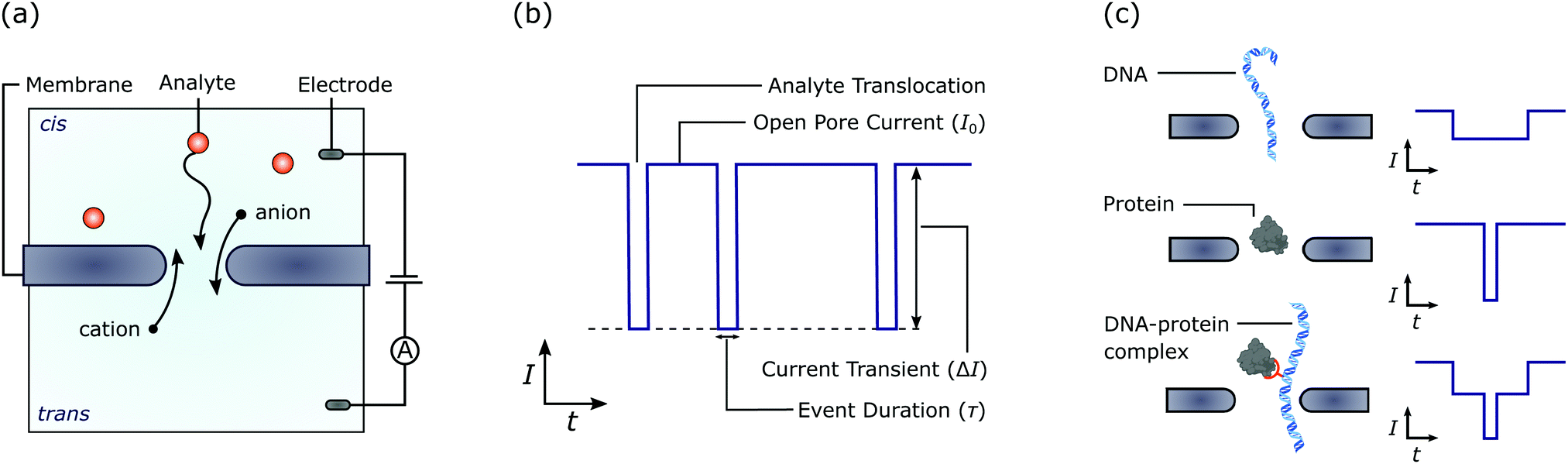 | ||
| Fig. 1 Schematics demonstrating the basic principle of ionic current based sensing using a solid-state nanopore. (a) A schematic of the experimental setup. A nanopore in a membrane (e.g. SiNx) separates two chambers of electrolyte solution (e.g. KCl). Applying a voltage across the membrane via electrodes (e.g. Ag/AgCl) results in a measurable ionic current. When a molecule translocates through the pore it affects the passage of ions resulting in a change in the ionic current. Depending on the properties of the molecule and electrolyte, the net ionic current may increase or decrease. (b) Schematic of a ionic current measurment trace. The magnitude of the change in current between the open and transient state, as well as the event duration can be used to infer properties such as the size and charge of the molecule. (c) Examples of the translocation of various biomolecules through a nanopore and schematics of the corresponding measurement trace. These schematics represent only a few examples of the vast array of molecules that have been sensed using solid-state nanopores. | ||
Interest in nanopore sensors has often focused on DNA sequencing,19 however, these devices have been used for a wide range of applications. In particular, nanopores have been developed for protein fingerprinting,20–22 polymer data storage,23,24 biomarker detection,12,25 enzymology,26 ultra-sensitive ion detectors,27 nanoparticle fabrication,28 and nanoscale chemical reactors29,30 to name only some. Given this wide range of applications, it is important to be able to vary the nanopore dimensions and operate these devices in a wide range of environmental conditions. In this regard, solid-state nanopores provide advantages over their biological counterparts. Moreover, solid-state nanopores can be more easily integrated with complementary nanostructures via well-developed semiconductor fabrication techniques. Such nanostructures can be used to enhance the detection capabilities of nanopores including increasing the detection bandwidth,31,32 enabling greater device densities,31 and providing sensitivity to molecular properties not possible using ionic current based detection.33–35
Given the potential of solid-state nanopores, a range of methods to fabricate these devices have been developed.36 In the past, these techniques had a large barrier to entry,37 lacked scalability,38 or showed difficulty in fabricating nanopores with diameters down to a few nanometres as required for many of the applications described above.39–41 Recently, several techniques have emerged whereby solid-state nanopores are fabricated in electrolyte solutions (i.e. the same environment which subsequent experiments are performed in42–45). These in situ nanopore fabrication techniques are promising as they offer methods to deliver pores with diameters down to a single nanometre in a matter of minutes and can be performed using easily accessible equipment. As a result, these fabrication methods are helping to democratise and increase the pace of solid-state nanopore research.
Here we review the latest advances in the field of in situ solid-state nanopore fabrication, whereby pores are fabricated directly in the environment in which sensing is performed. We will focus on techniques that enable the fabrication of nanopores with diameters of a few nanometres or less as required for many of the applications described above. These in situ nanopore fabrication methods can be categorised into four general techniques. These are (i) controlled breakdown (CBD), (ii) electrochemical reaction (ECR), (iii) laser etching, and (iv) laser-assisted controlled breakdown (la-CBD). We review each of these methods, discuss their advantages and challenges, and highlight future areas of research that may be pursued to optimise and enhance each technique. Moreover, each method is compared with the aim of providing researchers with insight into the preferable fabrication technique for a desired application.
1 Solid state nanopores
We will first provide a brief overview of solid-state nanopores. A recent review of solid-state nanopores for single-molecule biosensing applications can be found in ref. 46. Solid-state nanopores are typically fabricated in thin (<50 nm) low-stress SiNx membranes suspended above a Si handle. The fabrication of these devices is discussed elsewhere.47 Silicon is generally used as the substrate since fabrication processes for this material have been well developed by the semiconductor community (however glass substrates have also been used to reduce the device capacitance48,49 and therefore the high frequency noise50). Low-stress Si-rich SiNx is often used for the membrane given its mechanical stability, high resistivity, and dielectric strength.51 However, several other dielectric membranes have also been used. For example Al2O3,52,53 HfO2,54 and TiO255 have been used to improve the nanopore surface charge, pore stability, and membrane photoluminescence respectively. Two-dimensional membranes such as graphene,56,57 MoS2,58 hBN,59 WS260 and MXenes,61 have also received attention for nanopore applications. For these devices, a micron-sized aperture is typically fabricated in a SiNx membrane and the two-dimensional film suspended across the aperture.62 Solid-state nanopores have also been created in quartz capillaries,38 however, these devices have the drawback that they can not be integrated as easily with semiconductor processes for the up-scaling in production required for many applications.The most typical sensing strategy for solid-state nanopores is based on measuring changes in the ionic current through the pore due to analyte translocation. Here, a voltage is applied across the membrane resulting in a measurable ionic current through the nanopore [Fig. 1(a)]. When a biomolecule is drawn into and through the pore (typically via electrophoretic forces), it affects the passage of ions resulting in a measurable change in the ionic current [Fig. 1(b)]. The duration and amplitude of the change in ionic current can then be used to infer properties of the molecule such as the size, charge, and interactions with the pore surface [Fig. 1(c)]. In some cases, changes in the current level during a translocation event can also be used to infer the shape, dipole moment, and sequence of the translocating entity. Matching the diameter of the nanopore to be close, but slightly larger, than the size of the analyte generally maximises the signal, highlighting the need to fabricate pores with variable diameters down to a single nanometre. This sensing modality has demonstrated significant success in detecting a wide range of molecules, including but not limited to, DNA,63 RNA,64 proteins,65 and nanoparticles.66 However, this technique does suffer from several limitations such as restricted bandwidth as a result of high frequency noise.50 Moreover, each nanopore must be electrically and fluidically isolated to maximise the signal to noise ratio and avoid signal convolution which limits the attainable device density.31
To overcome these limitations, several alternative nanopore sensing strategies have been proposed and demonstrated. One such technique relies on integrating nanoelectrode structures such as field-effect sensors31,67–71 and electron tunnelling nanogaps72–76 with a nanopore. Changes in the current through these nanoelectrode structures occur as a result of analytes translocating through an integrated or nearby nanopore. Optical detection strategies have also received significant interest in recent years. These methods can be based on the detection of fluorescent labels,77,78 light scattering,79 and surface enhanced Raman spectroscopy.80–82 Optical based detection strategies are often enhanced by integrating plasmonic nanostructres with the nanopore.83–86 Given the ability of these alternate sensing modalities to overcome several of the fundamental limitations of ionic current based sensing, they will likely continue to attract interest in the coming years. It is therefore important for nanopore fabrication techniques to be able to integrate pores with the complementary nanostructures required for these alternate sensing strategies. Reviews focusing on nanopore sensing using complementary nanoelectrodes and optical detection can be found in ref. 87, 83 and ref. 88 respectively.
2 Chronology of solid-state nanopore fabrication
Before discussing in situ nanopore fabrication techniques, it is useful to provide a perspective of other methods used to fabricate solid-state nanopores. Given the significant interest in these devices, a number of techniques to fabricate pores have been demonstrated.36 As such, it is not practical to discuss all of these methods. Rather, we will focus on some of the most commonly used techniques. A timeline of the development of these techniques is shown in Fig. 2, as well as the approximate minimum pore size that has been demonstrated with each technique. Note that in some cases the fabrication technique shown in the timeline may have been used at a prior date to create larger nanopores not used for single-molecule sensing. Although there has not been a drastic change in the minimum nanopore diameter obtainable over the past two decades, there has been significant progress towards the development of accessible and reliable nanopore fabrication techniques using commonly available equipment and requiring minimal user expertise.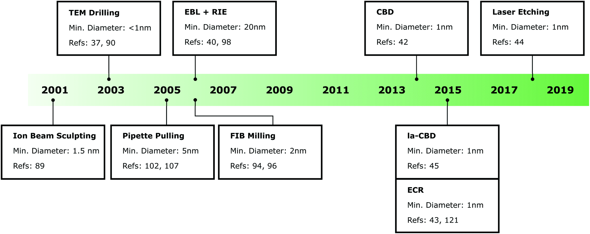 | ||
| Fig. 2 A timeline showing the development of different solid-state nanopore fabrication techniques. The approximate minimum pore diameter that has been obtained to date is also shown for each technique. The last four methods shown in the timeline are the in situ nanopore fabrication techniques. These techniques utilise equipment that is commonly found in a nanopore research laboratory and require significantly lower user expertise than many of the other methods. | ||
Solid-state nanopores with dimensions on the order of a few nanometres were first reported in 2001 using an ion beam sculpting technique.89 A bowl-shaped cavity was fabricated in a stoichiometric Si3N4 membrane using reactive ion etching. Following this, energetic Ar+ ions were used to thin the membrane on the opposite side to the cavity. When the planar surface intercepts the bowl-shaped cavity, a nanopore was created in the membrane. Nanopore formation was detected by monitoring the transmission of Ar+ ions through the membrane enabling the controlled fabrication of pores with diameters down to 1.5 nm.
Shortly after, solid-state nanopores were fabricated using a transmission electron microscope (TEM).90 In the initial demonstration of this, relatively large pores (∼20 nm) were first created in the membrane using electron beam lithography and anisotropic etching.90 The pore was then exposed to the electron beam from a TEM which fluidises the membrane. Depending on the pore size and membrane thickness, this can lead to shrinking of the nanopore diameter due to a decrease in surface tension. The nanopore diameter can be monitored in real time using the TEM and when the electron beam is removed the pore retains its shape thus enabling controlled fabrication of nanopores with diameters down to a single nanometre. However, currently it is more common to directly drill nanopores in a solid-state membrane using a TEM.37,91,92 Here, the membrane is subjected to a tightly focused electron beam with a spot size typically less than a few nanometres. When the high energy electrons (typically accelerated at ∼200 kV) interact with the membrane they cause sputtering of the material resulting in the formation of a nanopore.
Direct drilling of nanopores using charged particles can also be performed using a focused ion beam (FIB). This can be done using a range of different ions, however, Ga+ (ref. 93 and 94) and He+ (ref. 95 and 96) are currently the most common. These microscopes have wider beam profiles compared to a TEM thus reducing the obtainable resolution. Nanopores with diameters down to approximately 5 nm93 and 1.3 nm96 have been fabricated using Ga+ and He+ ions respectively. However, reproducibly obtaining such small pore sizes can be difficult and requires an experienced operator. Fabricating nanopores using a FIB has the advantage that (unlike in a TEM) multiple devices can be loaded into the microscope, thus enabling automated drilling of nanopores over relatively large areas.41 Drilling of nanopores in a FIB can also be largely automated (whereas a TEM is typically manually operated) making the production of nanopore arrays easier. Note that direct drilling of nanopores using charged particles can result in damage to surrounding nanostructures, making these techniques incompatible with some nanopore devices.40,74,97 Drilling nanopores using charged particles can also lead to changes in the fundamental membrane composition which may decrease the pore stability.54,92
Another technique used to fabricate solid-state nanopores relies on the well-developed nanofabrication techniques of electron beam lithography (EBL) and reactive ion etching (RIE).40,98,99 Here, nanopores are patterned into an electron sensitive resist using EBL and this pattern is transferred to the membrane via RIE. Similar to FIB milling, this technique can be used to create high density arrays of nanopores over large areas.39 However, it is challenging to reproducibly fabricate pores with diameters less than approximately 20 nm using this technique. The obtainable pore diameter can be reduced by performing atomic-layer deposition following nanopore fabrication100 or by using anisotropic etching rather than RIE to create the pore.101
All of the techniques discussed above have utilised specialised equipment which require highly trained personnel to operate. This initially limited the availability of solid-state nanopores to a relatively small community. Outside of the in situ nanopore fabrication methods which are the focus of this review, laser-assisted pulling of pipettes is one other fabrication technique that is democratising solid-state nanopores. These pores are typically fabricated from glass or quartz capillaries by the application of heat and applying a pulling force from each end of the capillary.102–106 By adjusting the fabrication parameters (e.g. applied heat, pulling force and time), it is possible to produce nanopipettes with opening diameters of several nanometres.107 While the simplest nanopipettes contain just a single nanopore at their tip, nanopipettes with two108 and four109 barrels, each containing a nanopore, have also been demonstrated. In these configurations, each nanopore is independently addressable and can be used for sensing and trapping with multiple pores. Moreover, the barrels can be selectively filled with conductive materials that can be used for field-effect gated molecular transport or to enable additional detection modalities.46,110 The surface of nanopipettes can also be easily functionalised via salinization chemistry to attach analyte-specific binding molecules, such as aptamers and antibodies for selective capturing and detection of analyte molecules with high specificity.111–114 As such, nanopipettes have been used for the detection of a range of analyte molecules including nucleic acids, proteins, and nucleic acid protein complexes.23,25,115–120 Nevertheless, their wider deployment is limited by difficulties in the production of pore arrays and nanopipettes with reproducible pore sizes.
The in situ pore fabrication methods described below have the potential to overcome the issues associated with these prevalent nanopore fabrication techniques. Most notably the in situ fabrication techniques; (i) require comparatively little capital cost and can be performed with equipment often found in research labs, (ii) do not require significant user experience, (iii) can fabricate pores in a matter of minutes and be integrated with common nano/micro fabrication techniques and, (iv) can create pores with diameters down to a single nanometre with real-time feedback on the pore size. The in situ nature of these pore fabrication techniques also minimises device contamination and facilitates easy wetting of the nanopore. The latter of these can be challenging for nanopores fabricated ex situ, especially for devices that do not allow for the use of harsh cleaning procedures to render the surface hydrophilic.121,122 However, as will be highlighted in the following sections, in situ nanopore fabrication techniques remain in varying stages of development with each method requiring continued research to reach its full potential.
3 Controlled breakdown
Controlled breakdown (CBD) is the most developed in situ nanopore fabrication technique having first been reported in 2014.42 This technique can be used to create nanopores in dielectric membranes (typically SiNx with thicknesses ≤30 nm123). Fig. 3(a) shows schematics of a typical experimental setup (i), nanopore fabrication measurement (ii), and pore formation mechanism (iii) for CBD. Here, an electric field in the range of 0.6–1 V nm−1 is applied across the membrane which results in a small, measurable leakage current. After a period of time, a jump in the current is observed signifying breakdown and nanopore formation. When this occurs, the voltage is quickly reduced to zero (typically within 1–100 ms42,124) to avoid catastrophic failure of the membrane. Note that, although a constant voltage is shown in the schematic of Fig. 3(a), CBD has also been performed by applying a voltage ramp,124 voltage pulses,125 and a constant current.126 Indeed, CBD is a general phenomenon and will result whenever a sufficiently large electric field is applied across the membrane. CBD can be performed using essentially the same experimental setup required for nanopore sensing with the addition of a voltage source capable of applying a potential of up to approximately 30 V (the specific voltage required will depend on the membrane being used). A current amplifier capable of measuring large currents and applying high voltages may also be required since most commercial amplifiers used for nanopore sensing are limited to apply 1 V and measure up to 200 nA.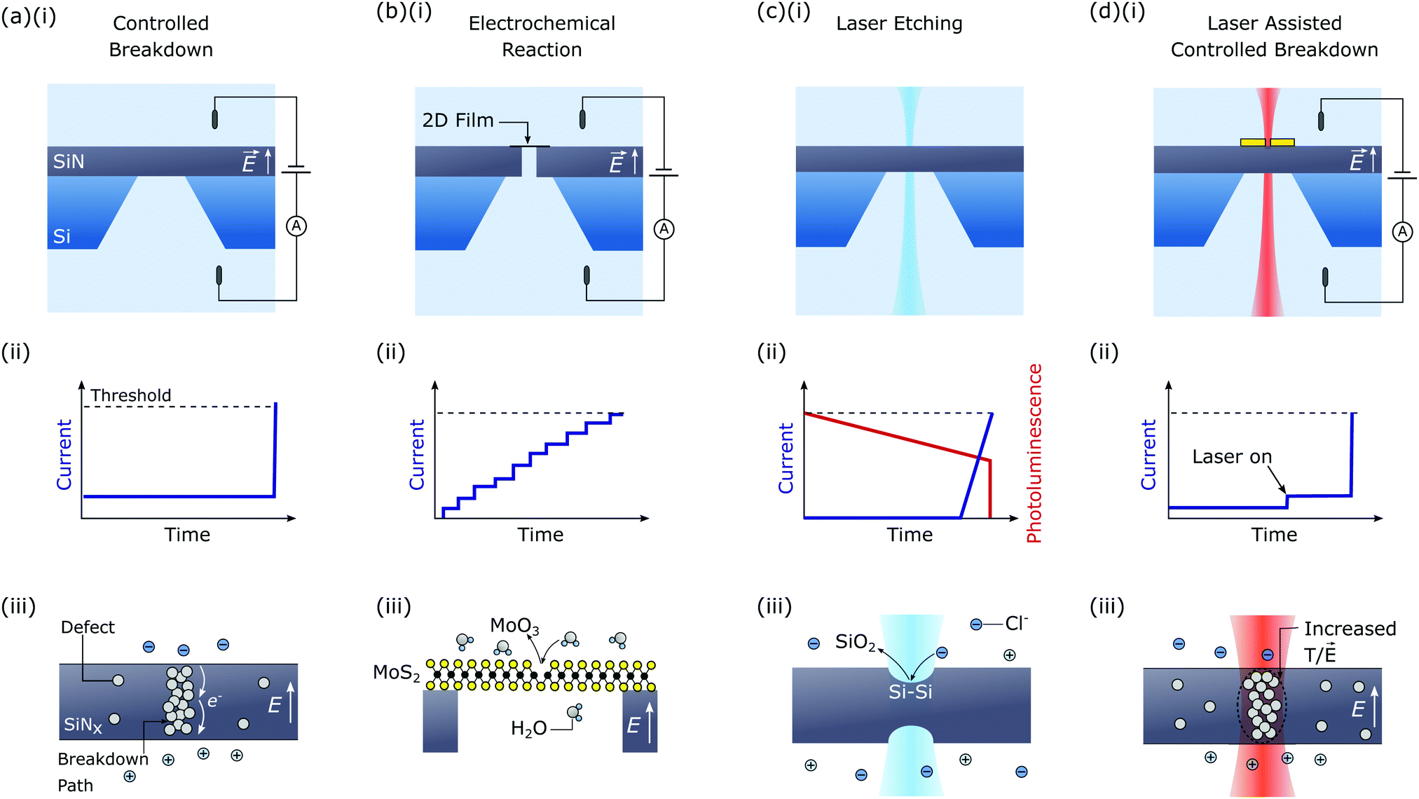 | ||
| Fig. 3 Schematics of the experimental setup (top), measurement trace (middle), and pore formation mechanism (bottom) for the four in situ pore fabrication techniques. (a) Controlled breakdown (CBD) whereby nanopores are formed by applying a large electric field (∼0.6–1 V nm−1) across a dielectric membrane. Such electric fields result in charge trap accumulation which form a percolation path and result in physical breakdown in the membrane as a result of Joule heating. (b) Electrochemical reaction (ECR) where nanopores are formed in suspended two-dimensional films due to electrochemical reactions originating from a defect in the film. (c) Laser etching whereby nanopores are formed as a result of photochemical etching of Si-rich SiNx membranes in solution. (d) Laser-assisted controlled breakdown (la-CBD) whereby a laser is focused on the membrane simultaneous to the application of an electric field to induce breakdown at the focal point of the laser. This can be due to either localised heating, laser etching or enhanced electromagnetic fields. Note that the threshold current shown in the experimental measurement trace schematics will not be the same magnitude for each technique. | ||
The mechanism of pore formation during CBD is generally assumed to result from the same process as dielectric breakdown in semiconductor devices. In particular, when an electric field is applied across a dielectric a leakage current flows through the material due to electric field assisted electron transport through charge traps (defects) in the dielectric. At some point, these charge traps form a percolation path leading to a spike in the current across the membrane.127,128 This increase in current results in physical damage to the dielectric, potentially as a result of significant Joule heating. However, it should be noted that the situation is somewhat more complex for CBD since here the electric field is applied via an electrolyte solution. As such, electrochemical reactions must occur at the membrane–electrolyte interface to inject and remove charge from the membrane.129,130 These electrochemical reactions may limit the leakage current across the membrane and therefore affect the breakdown dynamics. Indeed, it has previously been shown that the pH of the electrolyte solution significantly affects the voltage at which breakdown occurs.42,130
Following CBD, the diameter of the nanopore can be enlarged enabling tailoring of the pore size to the analyte dimensions. The maximum pore size has typically been limited to 20 nm to avoid the formation of multiple pores, although, as described below, methods to address this issue have recently been reported.131 Nanopore expansion is achieved by applying voltage pulses and measuring the pore conductance at low bias between each pulse to enable feedback on the pore size.122 The expansion voltage pulses should have reduced amplitude (∼0.3–0.5 V per nm membrane thickness) compared to the breakdown voltage to enable widening of a pre-existing pore while reducing the probability of creating additional pores.124,132 It should be noted, however, that pore enlargement via the application of voltage pulses proceeds via a fundamentally different mechanism to nanopore formation using CBD. Although not well understood, it was recently suggested that nanopore enlargement occurs via the electrochemical dissolution of membrane material along the pore walls driven by the flow of ionic current.131 A detailed description of the procedure to form nanopores via CBD and subsequent pore enlargement using large electric fields is provided in ref. 124. Software for the automation of the CBD procedure and a description of the hardware required is also available in ref. 124, highlighting the accessibility of this technique.
3.1 Advantages of controlled breakdown
In addition to its accessibility, CBD also possesses some unique advantages over other pore fabrication methods. Firstly, this technique does not require direct line-of-sight to the membrane. Rather, nanopores can be created using CBD as long as there is a fluidic connection between the electrodes and membrane. This opens up the possibility to fabricate nanopores integrated with complex, potentially non-planar, geometries not possible using other pore fabrication methods. Utilising this advantage, nanopores were fabricated in a SiNx membrane which was separated from a nanoporous membrane by a sub-micron sized cavity.135–137 Using this device structure, it was demonstrated that the conformation of DNA could be controlled by passing the molecules through the nanoporous membrane prior to translocation through the nanopore. This resulted in a narrower distribution of dwell times and in some cases a reduction in the number of folded translocation events, an important result for practical sensing applications. The ability to create nanopores via CBD without line-of-sight also enables the integration of nanopores within microfluidic nanostructures which can be used for multiplexing.138,139 Microfluidic structures have also been integrated with a nanopore to enable isotachophoretic140 and convection based141 focusing of analytes at the nanopore.Another advantage of CBD is that the breakdown process is a general phenomena and can be used to create nanopores in a range of membrane materials. This is in contrast to methods, such as laser etching, which rely on specific photochemical reactions to create pores. While most studies have created pores in SiNx,42,125,129,142–145 CBD has also been used to create pores in other dielectrics such as SiO2,42 TiO2,55 and HfO2.146 Nanopores have also been fabricated via CBD in membranes where gold was deposited on top of SiNx.147 This may be important for the fabrication of nanopore devices with integrated electrodes.40,74,148 Given the generalisability of this technique, one might anticipate seeing CBD extended to different dielectric materials such as sapphire149 and Al2O352,53 in the coming years.
Recent studies have also demonstrated the ability to control the surface properties of SiNx nanopores fabricated via CBD. Controlling the surface properties of solid-state nanopores is important to reduce pore clogging resulting from analyte–membrane interactions. Moreover, it offers a route towards selective biomolecular detection.71,150,151 It was recently demonstrated that adding NaClO to the solution during CBD resulted in a significant change in the nanopore surface charge even after the electrolyte was replaced.152 For DNA translocation experiments, this change in the surface charge resulted in an increased event frequency and less pore clogging due to reduced electrostatic interactions between the pore walls and the translocating molecule. The mechanism by which the addition of NaClO during CBD affects the nanopore surface charge is not well understood and may be an interesting area for future research. CBD has also enabled functionalisation of the pore walls with a number of molecules via photohydrosilylation.153 Such functionalisation of SiNx films generally requires the removal of a native oxide layer via hydrofluoric acid etching.154,155 However, this is not suitable for nanopore functionalisation as it results in unacceptable widening of the pore.153 Instead, the in situ nature of CBD means photohydrosilylation can be performed without exposing the pore to the atmosphere thus preventing the formation of a native oxide layer.
3.2 Challenges of controlled breakdown
Despite the promise of controlled breakdown, there are also several challenges in using this technique to create solid-state nanopores [Fig. 4]. One such challenge is that CBD can result in the formation of multiple nanopores123,132 [Fig. 4(b)]. The formation of multiple pores is a particular issue if the desired pore diameter is large (>20 nm). This is because, during the pore expansion phase, the membrane will be subjected to large electric fields for time periods comparable to those required to induce new breakdown events. However, it was recently shown that increasing the conductivity of the solution during the pore expansion phase decreased the probability of forming multiple pores. This is because nanopore expansion is driven by electrochemical reactions arising from significant ionic current flow through the pore. As such, increasing the conductivity of the solution allows higher current at lower potentials, thus enabling nanopore expansion with a decreased risk of new breakdown events occurring.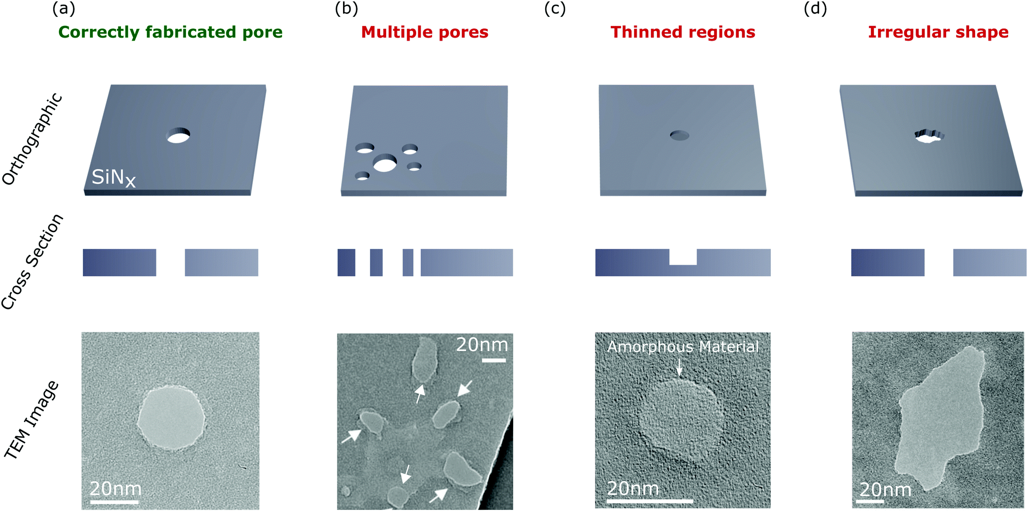 | ||
| Fig. 4 Orthographic schematic (upper), cross-section schematic (middle), and TEM images (lower) of some commonly encountered issues when fabricating nanopores via CBD. (a) A correctly fabricated pore. (b) Multiple pores forming in the membrane. Such pores can occur in close proximity to each other (as shown in the TEM image) or as independent events in different regions of the membrane. (c) Formation of thinned regions in the membrane. Significant conductance (nanosiemens) can result from such thinned regions. (d) Irregularly shaped pores. Such irregular shaped nanopores become increasingly evident when pores are expanded to large diameters (≥20 nm) and may lead to a misinterpretation of the translocation data. TEM images were taken with permission from (a–c) ref. 133 and (d) ref. 134. | ||
Despite these advances, it still may be useful for researchers developing CBD techniques to test if the protocol/experimental conditions being used result in the formation of multiple nanopores. Unfortunately, multiple pores can not be easily distinguished from a single pore using conductance measurements (although more information can be obtained by performing translocation experiments121,131). As a result, several techniques have been developed to detect the presence of multiple pores created via CBD. One method is to measure the change in pore conductance resulting from coating the pore in a self-assembled monolayer.21,132,156 The basis of this technique is that coating multiple small nanopores will result in a larger change in the conductance than coating a single pore of equivalent area. Unfortunately, it is difficult to obtain conclusive results using this method since incomplete coating of the pore leads to significant uncertainties.132
Fluorescence microscopy has also been used to detect the presence of multiple pores created during CBD. This technique utilises Ca2+ and a Ca2+ indicator dye such as Fluo-4 to create a highly localised fluorescent signal at the nanopore opening.157,158 This enables the detection of multiple nanopores as well as the position of each pore with sub-diffraction limit resolution.158 Indeed, using this technique it was demonstrated that for one batch of devices, a disproportionate number of nanopores created via CBD form at the membrane edge (for another batch of devices the pores formed at random locations).158 Although the reason for this remains unclear, the fact that this phenomena is batch dependent suggests that it results from variations in the fabrication process. Spatial constrains may alter the translocation dynamics of long biomolecules with a radius of gyration comparable to the distance between the pore and the membrane edge. Laser-enhanced ionic current mapping can also be used to detect multiple nanopores and determine the position of each pore.159 Here, a laser is scanned across the membrane while simultaneously measuring the ionic current through the nanopore. When the laser position is aligned with the nanopore, an increase in ionic current is observed due to localised photothermal heating resulting in a decreased electrolyte viscosity.160
It has generally been assumed that the formation of multiple nanopores during CBD occurs as independent processes, with each pore forming at random locations in the membrane. It was therefore thought that by ensuring the time-to-breakdown is much longer than the time required to reduce the voltage once breakdown is detected, the formation of multiple pores could be avoided.129 However, TEM imaging of nanopores formed by CBD demonstrated that without adequate feedback conditions for membranes that require large voltages to undergo breakdown (>20 V), multiple pores may be formed in close proximity to each other [Fig. 4(b)]. The presence of multiple pores could not be explained by the statistics governing independent breakdown events. Instead, it was suggested that Joule heating, resulting from large ionic current through the initial nanopore, can lead to localised heating of the substrate promoting subsequent adjacent breakdown events.133 Unfortunately, due to limits in resolution, the fluorescence microscopy and laser-enhanced current mapping techniques can not easily distinguish between pores in close proximity.
Another interesting result obtained from TEM imaging nanopores fabricated via CBD is that this process can result in the formation of a thinned region in the membrane rather than a nanopore [Fig. 4(c)].133,134 Interestingly, these thinned regions demonstrated non-negligible transmembrane conductance (tens of nanosiemens) but could be distinguished from nanopores due to significant rectification in the measured current.133,134 Unfortunately, it is not clear whether such thinned regions are a widespread phenomena that have remained undetected in other studies, or are specific to the experimental conditions used in these works. It is noted that for SiNx films thicker than 10 nm, the effective length of the nanopore fabricated via CBD has been reported to be approximately one third of the membrane thickness.125,143,144,158 This suggests that membrane thinning may be present in these studies as a precursor step to pore formation. Further to this point, it was shown that such thinned regions can be penetrated to form nanopores by applying voltage pulses of opposite polarity to the initial breakdown voltage.133 Such pulses are routinely applied during what is assumed to be a pore expansion phase. However, following the above study, it may be the case that in some works these voltage pulses are penetrating a thinned region rather than expanding a pre-existing nanopore. Performing CBD in a high pH solution (pH > 12) can also create nanopores rather than thinned regions in the membrane.134 However, in general the best results in the literature (in terms of consistency of creating nanopores of a desired diameter) have been obtained at pH 8–10.124
Lastly, CBD can result in irregularly shaped nanopores [Fig. 4(d)] which are particularly apparent for large pore diamaters (>20 nm). Such irregularly shaped pores may result in a misinterpretation of the ionic current changes resulting from the translocation of a biomolecule through the nanopore. While we have highlighted some of the challenges of CBD above, it should be emphasised that this remains a powerful technique to create nanopores with diameters down to a single nanometre. Many of the challenges described above can be largely avoided by optimising the fabrication procedure for a given membrane composition/geometry and electrolyte environment. Indeed, it was recently shown that using optimised procedures, CBD could create nanopores with acceptable properties for sensing experiments in approximately 85% of cases.124 It is hoped that this value will continue to increase with further studies into the fundamental CBD process.
3.3 Advanced controlled breakdown methods
One of the challenges of CBD is that the stochastic nature of the process results in nanopores forming at random locations in the membrane. This is particularly problematic if pores are to be integrated with complementary nanostructures required to enable sensing modalities in addition to ionic current based detection. Positioning of nanopores is also required for dual nanopore devices which have been used to control the translocation dynamics of biomolecules.161–163To overcome this issue, various techniques have been demonstrated that enable positioning of nanopores fabricated via CBD. These techniques are shown in Fig. 5, along with a schematic representing how each method has been achieved to date. The first of these methods relies on selectively thinning a portion of the membrane [Fig. 5(a)]. Given the breakdown voltage depends approximately linearly on the membrane thickness,143 this will result in nanopores forming at the thinnest part of the membrane. This technique has been demonstrated using a He+ FIB164 and EBL followed by RIE12,158 to locally thin regions of the membrane. However, the large capital cost of these instruments limits the availability of this method for many researchers. Rather than thinning the membrane, a dielectric could also be patterned on the membrane surface to localise nanopore formation.
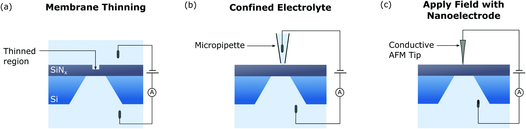 | ||
| Fig. 5 The three advanced CBD methods that can be used to control the nanopore position and examples of each method. (a) Controlling the nanopore position by thinning a region of the membrane. This has previously been demonstrated using a He-FIB/EBL+RIE to thin the membrane. (b) Controlling the nanopore position by confining the electrolyte on one side of the membrane. This has been demonstrated by using a micropipette in contact with the membrane (as shown in the schematic) or microfluidics structures on the membrane surface. (c) Controlling the nanopore position by applying the electric field with a nanoelectrode. This has been demonstrated using a conductive AFM tip to apply the electric field. | ||
Another technique to control the position of CBD created nanopores is to confine the electrolyte on one side of the membrane. This has previously been done using a micropipette filled with electrolyte to contact the top of the membrane.126,165 Performing CBD by applying the breakdown voltage between the electrolyte in the pipette and a backside reservoir resulted in pore formation localised to the area where the meniscus contacts the membrane (∼1 μm in diameter). Controlling the pipette position using a micromanipulator enabled the creation of high density arrays of nanopores thus significantly increasing the number of biosensing experiments that can be performed per membrane.126 Nanopore position can also be controlled by confining the electrolyte using microfluidic structures fabricated on top of the membrane.138
The last advanced CBD method that enables control over the position of the fabricated nanopore relies on localising the electric field by applying the voltage via a nanoelectrode. This has been achieved by applying a large voltage between a conductive atomic force microscope (AFM) tip and a backside electrolyte reservoir.166 The small diameter of an AFM tip (∼10 nm) enables highly localised positioning of the nanopore. As a result, large electric fields can be applied with a reduced probability of forming multiple pores, thus enabling rapid nanopore fabrication. However, this technique is not truly in situ as devices must be transferred to a setup whereby electrolyte is present on both sides of the membrane to perform sensing.
To date, these techniques have demonstrated limited ability to integrate nanopores with complementary nanostructures. Methods discussed above that rely on confining the electrolyte on one side of the membrane demonstrate insufficient localisation for this to be possible. In the case of breakdown using an AFM tip or thinning of the membrane using a FIB/EBL+RIE, integration with complementary nanostructures is likely possible. However, this would necessitate time consuming alignment processes that require significant user input. As discussed in Section 6, la-CBD has been used to self-align nanopores with plasmonic nanostructures.45 However, this method is limited in that it can only be used to integrate nanopores with plasmonic nanostructures. Advanced CBD techniques that enable self-alignment with other nanostructures, such as field-effect sensors and tunnelling nanogaps, would greatly ease the fabrication of these devices. This would represent significant progress in the development of these devices, which have often been limited by their time consuming and low yield fabrication processes.68,167,168
4 Electrochemical reaction
The next in situ nanopore fabrication technique that we will discuss is electrochemical reaction (ECR). Schematics of the experimental setup, measurement trace, and pore formation mechanism for ECR are shown in Fig. 3(b). Like CBD this technique can be performed using the equipment required for nanopore sensing with the addition of a voltage source capable of supplying up to ∼10 V.The term ECR was first coined in 2015 when using a large electric field to create nanopores in a MoS2 film suspended above an aperture in a SiNx membrane.43 Here, the transmembrane voltage was increased in steps of 100 mV while simultaneously monitoring the current. When the transmembrane voltage reached 800 mV, an increase in the current was observed indicating nanopore formation. The voltage was then maintained at 800 mV to expand the nanopore until the measured current exceeded a predefined threshold, at which point the voltage was reduced to zero. In this process, nanopore formation was assumed to initiate at a defect in the film and then widen via electrochemical removal of exposed atoms. Removal of atoms was thought to result from the oxidation of MoS2 to MoO3 which detaches into solution [Fig. 3(b)(iii)], however, the oxidation of MoS2 into other valence states was not discounted. Interestingly, step-like increases in the current are observed during ECR indicating the electrochemical removal of single atoms from the lattice.43 Studies have demonstrated that the threshold voltage at which pore formation occurs can range between 800–2500 mV and depends on the number of MoS2 layers, the presence of contamination, and the film quality.62
Nanopores have also been created in suspended graphene films via ECR.43,121,169 The first demonstration of this121 utilised voltage pulses with an amplitude of 7 V and a duration of 250 ns to create nanopores. Following pore formation the pulse amplitude was decreased to 5 V to reduce the probability of forming multiple nanopores. By applying a self-assembled coating after nanopore formation and measuring the resulting change in conductance it was demonstrated that this technique was able to reproducibly create single nanopores. To better understand the mechanism of nanopore formation, a recent study used in situ atomic force microscopy to image supported graphene films when a large voltage is applied between the graphene and an electrolyte solution.169 Here, etching of the graphene originating at the grain boundaries (which contain defects) was observed. This study also utilised the voltage pulse protocol described above (albeit with longer durations of 50 ms) to create nanopores in graphene films suspended across an aperture in a glass chip. The use of glass chips decreased the device capacitance, thus reducing the high frequency noise in ionic current measurements.50
Given the above discussion, it may be clear to the reader that ECR utilises the same experimental procedure as CBD. In particular, an electric field is applied across the membrane to induce nanopore formation while the resulting current is monitored as a feedback mechanism. As such, it is worth highlighting how these two techniques relate to each other. As previously discussed, the leakage current during CBD (which drives nanopore formation) is determined by two processes, (i) electrochemical reactions that occur at the membrane interface to inject electrons into the membrane and, (ii) charge transport across the membrane, generally assumed to be through defects in the dielectric. For the case of two dimensional conductive materials such as graphene and MoS2, charge transport across the membrane does not limit the pore formation process. Rather, nanopore formation is assumed to proceed as a result of electrochemical reactions that occur at a defect in the membrane. Based on this understanding, it is perhaps useful to think of ECR as a unique case of CBD that arises when scaling down to a two-dimensional membrane whereby charge transport across the membrane no longer limits nanopore formation. We stress however, that this understanding is based on current descriptions of these processes in the literature. Indeed, there have been few studies on the mechanism of pore formation via ECR to date. One simple study would be to vary the electrolyte composition during ECR to better understand the mechanism of pore formation.
Creating nanopores in two-dimensional materials has several advantages compared to pores in thicker dielectric membranes. The atomic thickness of these films leads to a larger ionic current (and a larger blockade current resulting from molecule translocation) compared to equivalent sized pores in thicker SiNx membranes.56,170 These nanopores have also received significant attention in polymer sequencing applications due to their atomic thickness.58,171–173 For example, in DNA sequencing applications the thickness of graphene is comparable to the spacing between nucleobases along a DNA strand (although multiple nucleobases may still contribute to the signal due to the access resistance of the pore14). This may simplify the complex signal decovolution processes currently required to sequence DNA using biological nanopores where multiple bases reside within the pore at a given time. Graphene and MoS2 can also be used as field-effect sensors56,69,167,174 that when integrated with nanopores offer larger detection bandwidths and increased device densities compared to what is possible using ionic current measurements.
Despite the promise of this method, there still remains research that should be performed to further develop ECR as a reliable nanopore fabrication technique. Firstly, as discussed above, performing ECR in different electrolyte compositions should provide further insight into the mechanism of pore formation during this process. A better understanding of this would aid in developing protocols for this technique to reproducibly create single nanopores of a desired size in a range of two-dimensional membranes. The ability to fabricate high quality, suspended, two-dimensional films is also challenging. This process usually involves growing the film on a substrate such as copper or sapphire (depending on the film being grown) and then transferring it to SiNx membranes with pre-patterned apertures. However, the transfer process may damage the film and usually requires a polymer coating which leaves unwanted residues.175 Optimised methods for transferring MoS2 films to apertures in SiNx membranes on the wafer scale have been published,62,176 however, transfer was only successful in 70% of the devices.176 To overcome this, a method to grow MoS2177 and graphene178 directly over apertures in SiNx membranes has been developed. However, it remains challenging to create single layer films using this technique.62 Lastly, it should be noted that nanopores in two-dimensional membranes typically display increased low frequency noise compared to dielectric membranes.179 This is thought to be a result of mechanical fluctuations in the membrane and limits the obtainable signal to noise ratio for these nanopores.179
5 Laser etching
Laser etching is a technique that enables the fabrication of nanopores with diameters down to a single nanometre using a low power (approximately 10 mW), highly focused laser and a confocal microscope.44 As discussed below, laser etching has only been demonstrated in Si-rich SiNx membranes using a blue-green laser. Etching of the membrane is induced by photochemical destabilisation of Si–Si bonds, resulting in localised thinning of the membrane and eventually pore formation. Nanopore formation and subsequent expansion can be tracked by applying a small transmembrane voltage (∼200 mV) simultaneous to laser illumination and monitoring the resulting ionic current. Schematics of the experimental setup, measurement trace, and pore formation mechanism for laser etching are shown in Fig. 3(c).The experimental setup required for laser etching is slightly more complex than for CBD/ECR. A detailed depiction of it is shown Fig. 6. The equipment required for laser etching may already be found in single-molecule biosensing research laboratories. The laser etching setup consists of a high numerical aperture objective (ca. 1.2) mounted on a confocal microscope for spatially resolved laser illumination of the membrane. An electron multiplying charge coupled device (EMCCD) camera is used for wide-field viewing and an avalanche photodiode (APD) detector for monitoring the photoluminescence (PL) from the SiNx membrane.44 The SiNx membrane is enclosed in an optically accessible fluidic cell and a low noise current amplifier is used to measure the ionic current during nanopore formation and for subsequent sensing experiments.
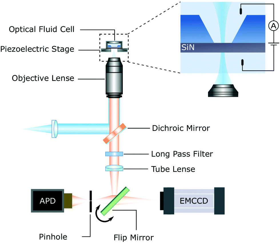 | ||
| Fig. 6 A typical experimental setup for laser etching (variations are possible). Drilling of a nanopore is induced by illuminating the membrane with a blue-green laser with milliwatt power focused on the membrane using a high numerical aperture objective. The emitted light is collected by the objective, filtered, and directed to an avalanche photodiode (APD) detector for monitoring of the photoluminescence. The emission pathway can be switched to a Electron Multiplying Charge Coupled Device (EMCCD) using a flip mirror for wide field viewing. The formation of a nanopore is tracked by monitoring the ionic current across the SiNx membrane induced by the application of a small transmembrane bias (∼200 mV). Figure adapted with permission from ref. 44. | ||
Following the initial demonstration, several works have studied the mechanism by which a focused laser induces etching of a SiNx membrane.180,181 It was shown that etching resulted from photochemical destabilisation of Si–Si bonds in the membrane material. In particular, blue-green light activates charge separation between Si bonds leading to their destabilisation. This process was observed to depend on the Si content of the membrane with small increases in the Si![[thin space (1/6-em)]](https://www.rsc.org/images/entities/char_2009.gif) :N ratio significantly enhancing the etch rate due to an increased density of dangling Si bonds at the membrane surface.181 Upon illumination, the photoactivated Si forms transient compounds with the anions (e.g. Cl−) present in solution.180 These transient compounds form SiO2 upon oxidation that solubilises in water resulting in etching of the membrane. Indeed, an increased anion concentration at the membrane–electrolyte interface was shown to accelerate pore formation.180 Similarly, the etch rate is increased in alkaline solutions as a result of enhanced hydrolysis of SiO2 by the hydroxyl ions in solution.181
:N ratio significantly enhancing the etch rate due to an increased density of dangling Si bonds at the membrane surface.181 Upon illumination, the photoactivated Si forms transient compounds with the anions (e.g. Cl−) present in solution.180 These transient compounds form SiO2 upon oxidation that solubilises in water resulting in etching of the membrane. Indeed, an increased anion concentration at the membrane–electrolyte interface was shown to accelerate pore formation.180 Similarly, the etch rate is increased in alkaline solutions as a result of enhanced hydrolysis of SiO2 by the hydroxyl ions in solution.181
Laser etching is a particularly promising pore fabrication method for optical based nanopore sensing techniques. These sensing strategies can be based on the detection of fluorescent labels,77,116 light scattering,79 and surface enhanced Raman spectroscopy.80,81 However, the need for precise alignment of the optical path with the nanopore remains a bottleneck for these experiments. Nanopores fabricated via laser etching partially overcome this issue by creating pores that are self-aligned with the optical path (although stage drift can be problematic and result in misalignment). Moreover, laser etching can also be used to create high density arrays of nanopores.181 This is useful for optical nanopore sensing techniques whereby the signal from each nanopore can be read out independently without the need for electronic and fluidic isolation.77 Additionally, laser etching creates ultra-thin nanopores (∼5 nm) since pores are formed from a thinning process. As discussed in the previous section, thin nanopores are preferable to enhance the signal amplitude and enable increased spatial resolution along the length of a translocating molecule.
Continued research into laser etching should extend the capabilities of this technique. In particular, while it has been demonstrated that this technique can be used to create nanopores in Si-rich SiNx films, it remains to be seen if it can be extended to other dielectric membranes. However, in situ laser illumination has been used to widen preexisting nanopores60 and create nanoporous membranes182 in WS2 films. Similar to the other in situ nanopore fabrication techniques described here, laser etching can also be susceptible to forming multiple undesired nanopores. In particular, it was demonstrated that multiple nanopores form in close proximity if laser illumination is not terminated shortly after pore formation181 (i.e. within a matter of seconds). As such, laser etching protocols may require further optimisation to enable the creation of single nanopores with diameters larger than 10 nm.
6 Laser-assisted controlled breakdown
The last in situ pore fabrication technique we will discuss is laser-assisted controlled breakdown (la-CBD). Schematics of the la-CBD experimental setup, experimental trace, and nanopore formation mechanism are shown in Fig. 3(d). Similar to the CBD approach discussed in Section 3, this method relies on applying a large electric field across a dielectric membrane. However, here a laser with power of approximately 5–50 mW is also focused on the membrane, resulting in breakdown occurring at the focal point of the laser. As shown in Fig. 7, there are three mechanisms by which this can occur. These are; (i) localised thinning due to photochemical etching, (ii) localised heating, and (iii) enhanced electromagnetic field. In general, all of these mechanisms may contribute to breakdown when a laser is focused on the membrane. However, as discussed below, the relative contribution of each mechanism will depend on the experimental conditions, such as membrane material, electrolyte composition, laser wavelength, and the presence of any plasmonic nanostructures.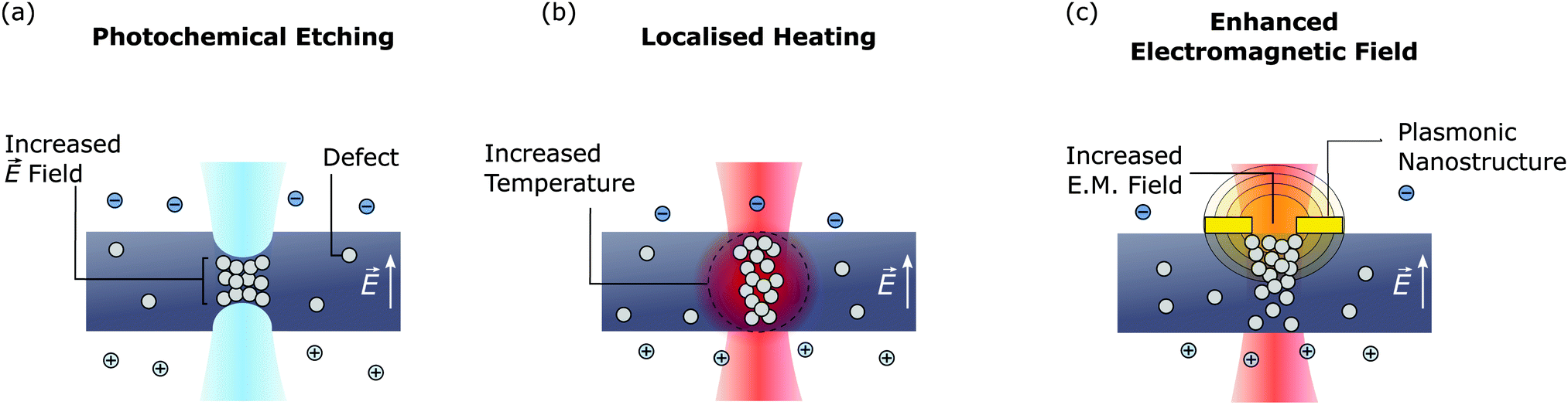 | ||
| Fig. 7 The three mechanisms by which laser illumination can assist in controlled breakdown. These are (a) laser etching, (b) localised heating, and (c) enhanced electromagnetic field. Each of these mechanisms may be present in a given la-CBD experiment. However, their relative contributions will depend on the experimental conditions such as laser wavelength, membrane material, electrolyte composition, and the presence of plasmonic nanostructures. | ||
The first of these la-CBD mechanisms relies on localised thinning of the membrane due to laser induced etching [Fig. 7(a)].180 Such photochemical etching was described in Section 5 and relies on illuminating a Si-rich SiNx membrane with a highly focused blue/green laser to destabilise Si–Si bonds.181 Performing CBD simultaneous to laser illumination results in breakdown occurring at the focal point of the laser180 given the membrane is thinnest in this region. Moreover, by varying the laser power and the electric field strength, it is possible to control the length of the created pore. This is typically challenging to do using other pore fabrication techniques and may be desirable depending on the chosen application. For example, ultra-thin membranes are advantageous for polymer sequencing applications.170,173,183 On the other hand, longer pores may be preferable when analysing the signal from larger, non-linear molecules such as proteins, as changes in the current transient during a translocation event can unveil information on the shape, rotational properties and dipole moment of the molecule.21
The second la-CBD mechanism that has been demonstrated relies on localised heating of the membrane [Fig. 7(b)]. Here, an infrared laser was used which induces negligible etching in the membrane.132 It was shown that performing CBD simultaneous to laser illumination results in pore formation at the focal point of the laser.132 This was attributed to a local increase in the temperature of the membrane, which lowers the electric field strength required to cause breakdown in SiNx.127,128 Based on the change in nanopore conductance during laser illumination, the local increase in temperature was estimated to be ∼8 °C.160 The authors also studied the formation of multiple pores by measuring the change in conductance resulting from a self-assembled monolayer coating. Here, it was demonstrated that continuing to focus the laser on the nanopore during pore expansion using large electric fields122 significantly decreased the probability of forming multiple nanopores when the desired diameter is 20–50 nm.132 Such large nanopores enabled the authors to translocate proteins through the pores and extract information about the size and shape of each molecule. It has also been suggested that a local increase in leakage current through the dielectric resulting from photoconductivity of SiNx under laser illumination may lead to localised breakdown.184 In practise, however, it may be hard to distinguish this effect from la-CBD resulting from localised heating.
The last la-CBD mechanism that has been demonstrated relies on enhancing the local electromagnetic field to induce breakdown [Fig. 7(c)]. This method was demonstrated by fabricating a plasmonic bowtie on a SiNx membrane.45 When this plasmonic nanostructure is illuminated by a laser, it creates a highly localised optical hotspot at the centre of the bowtie. By performing CBD simultaneous to laser illumination, it was shown that nanopores form at the centre of the bowtie, which was attributed to an increase in the local electromagnetic field. This method is appealing as it creates nanopores that are self-aligned with a plasmonic nanostructure. Such devices have received significant interest in recent years83,84 as they can increase the detection bandwidth of nanopores,185–187 provide sensitivity to molecular properties not possible using ionic current measurements,188,189 and control the translocation dynamics of biomolecules.79,190 Indeed, this is the only method discussed that has demonstrated self-alignment of nanopores with complementary nanostructures. This represents significant progress in the development of nanopore devices integrated with complementary nanostructures, which have typically relied on challenging fabrication processes.68,168
7 Comparison of techniques
One of the advantages of in situ nanopore fabrication techniques is that they have a low barrier for entry. Therefore, these techniques are highly appealing to researchers entering the field of solid-state nanopores. The equipment available to a researcher is one of the main considerations when deciding which of these techniques to use. For instance, if the researcher has easy access to optical equipment, then laser etching or la-CBD may be the preferable nanopore fabrication method (although it is noted that an optically accessible fluidic cell may be more complex than that usually required for nanopore sensing). If this is not the case, then CBD or ECR are perhaps better options as the experimental setup required for these techniques is somewhat less complex.On top of basic considerations such as equipment available, the choice of technique will also be dictated by the experimental need. For example, fabricating nanopores in ultra-thin membranes minimises the pore resistance thus increasing the signal amplitude resulting from a translocating molecule. Therefore, for applications that are limited by the signal to noise ratio, it may be preferable to fabricate pores via laser etching (ECR could also be used to create pores in 2D membranes however these devices show large noise levels179). On the other hand, applications which require long-term nanopore stability may require pores to be fabricated in HfO2 membranes (which offer increased stability compared to SiNx191). As such, CBD may need to be used for nanopore fabrication. Although the above examples only represent a few of the necessary considerations, it is hopefully clear that one in situ nanopore fabrication technique may not be optimal for all desired applications. Rather, it is envisioned that a researcher could select a given technique based on the desired application. This should be possible given the accessibility of each method.
In Table 1 we show a comparison of some of the important considerations when choosing an in situ nanopore fabrication technique. This includes the additional equipment required, the membrane materials it has been demonstrated on, whether the technique requires manual steps, the approximate fabrication time, the demonstrated pore diameters to date, and the resulting pore length. The additional equipment required shown in the table should only be used as a guide, as variations in the nanopore fabrication procedures are possible and may have different equipment requirements. The fabrication time is also an estimate taken from the literature and may vary depending on the exact protocol used. Another useful consideration not shown in the table is the cost of the equipment for each technique. In general, the cost to build a new experimental setup for laser etching or la-CBD (ca. £50000–100000) is an order of magnitude larger than CBD and ECR (ca. £1000–10000). However, we emphasise this cost is only a rough estimate and may be reduced by purchasing second hand hardware or developing in house equipment. Moreover, some of the experimental equipment required may already be present in many single-molecule biosensing labs that are looking to expand into solid-state nanopore research. The precision of each technique is also an important consideration. The precision of CBD and ECR has been reported to be approximately ±1 nm. While the precision of laser etching and la-CBD has not been reported in the literature, it is likely that with the optimisation of these techniques a similar value will be obtained. We hope that Table 1 and the discussion above will be a useful starting point for researchers deciding which fabrication technique is optimal for their desired application.
| Technique | Additional equipment required | Materials | Manual steps? | Fabrication time | Demonstrated pore diameter | Resulting pore length |
|---|---|---|---|---|---|---|
| a t is the membrane thickness. | ||||||
| CBD | •High voltage source (up to ∼±30 V) | SiNx, SiO2, HfO2, TiO2, metalised SiNx | No | ∼30 min | ≤20 nm | 1/3t − ta |
| •Current amplifier capable of measuring at high voltages | ||||||
| ECR | •High voltage source (up to ∼±10 V) | Graphene, MoS2 | No | ∼5 min | ≤10 nm | 2D |
| •Current amplifier capable of measuring at high voltages | ||||||
| Laser etching | •Milliwatt power laser (∼488 nm) | Si-rich SiNx | Focusing laser | ∼5 min | ≤10 nm | ≤5 nm |
| •Inverted microscope with high numerical aperture objective | ||||||
| •Optically accessible fluidic cell | ||||||
| •Piezoelectric stage | ||||||
| •Avalanche photodiode detector | ||||||
| •EMCCD | ||||||
| la-CBD | •Laser (wavelength and power depending on the procedure) | SiNx | Focusing laser | ∼30 min | ≤50 nm | Depends on procedure |
| •Inverted microscope with high numerical aperture objective | ||||||
| •Optically accessible fluidic cell | ||||||
| •Piezoelectric stage | ||||||
| •High voltage source (up to ∼±30 V) | ||||||
| •Current amplifier capable of measuring at high voltages | ||||||
8 Outlook
Solid-state nanopores are highly promising single-molecule sensing devices for a wide range of applications. These devices have already been used to study a range of biological and chemical processes. There has also been significant progress in recent years towards nanopore sensing in complex biological media,12,13,192 thus paving a way towards the commercialisation of solid-state nanopore devices for point-of-care diagnostics. In situ nanopore fabrication techniques have the potential to advance both of these research directions. In particular, the low barrier to entry of these techniques promises to make solid-state nanopores widely accessible to the research community. Moreover, these techniques can rapidly produce nanopores at low cost using largely automated processes. In situ nanopore fabrication techniques may therefore offer a path towards the fabrication of these devices for commercial applications.Although much research has already been done into the development of in situ nanopore fabrication methods, these techniques will benefit from continued research. Developing an increased understanding of the mechanism by which nanopores are formed via CBD, as well as the dependence on membrane material and environmental conditions would be beneficial. This would likely further increase the ability of this technique to create nanopores with optimised properties. CBD would also benefit from the development of techniques that enable the easy alignment of nanopores with complementary nanostructures. ECR is currently limited by difficulties in fabricating high quality two-dimensional suspended membranes. It is hoped that this technique will continue to develop as the synthesis and integration of two-dimensional materials continues to mature in the coming years. This may enable the development of ECR for other two-dimensional materials such as MXenes.193 Such materials may be of interest given the ability to easily functionalise their surface, thus potentially enabling tailoring of the nanopore properties for a given application.61 Laser etching is the most recently developed in situ pore fabrication method. Further studies on using this technique to create nanopores in a range of membrane materials will be of interest. Overall, in situ nanopore fabrication techniques are already significantly advancing solid-state nanopore sensors, however, it is hoped that further research into these techniques will continue to enhance their capabilities leading to a range of exciting new platforms for single-molecule sensing.
Conflicts of interest
J. Y. is a principal in Nanopore Solutions which produces fluidic devices that can be used for in situ nanopore fabrication and nanopore studies. All other authors have no conflicts to declare.Acknowledgements
J. Y. was funded by an FCT contract according to DL57/2016, [SFRH/BPD/80071/2011]. Work in J. Y.s lab was funded by national funds through FCT – Fundação para a Ciência e a Tecnologia, I. P., Project MOSTMICRO-ITQB with ref. UIDB/04612/2020 and UIDP/04612/2020 and Project PTDC/NAN-MAT/31100/2017. J. F. would like to thank the Oxford Australia Scholarship Committee and the University of Western Australia for Funding. A. I. and J. E. acknowledge support from BBSRC grant BB/R022429/1, EPSCR grant EP/P011985/1, and Analytical Chemistry Trust Fund grant 600322/05. This project has also received funding from the European Research Council (ERC) under the European Union's Horizon 2020 research and innovation programme (grant agreement No 724300 and 875525). J. M. was supported through the UKRI Future Leaders Fellowship, Grant No. MR/S032541/1, with in-kind support from the Royal Academy of Engineering.References
- J. K. Rosenstein, S. G. Lemay and K. L. Shepard, Wiley Interdiscip. Rev.: Nanomed. Nanobiotechnol., 2014, 7, 475–493 Search PubMed.
- Y. Li, L. Zhao, Y. Yao and X. Guo, ACS Appl. Bio Mater., 2019, 3, 68–85 Search PubMed.
- W. J. Greenleaf, M. T. Woodside and S. M. Block, Annu. Rev. Biophys. Biomol. Struct., 2007, 36, 171–190 CrossRef CAS.
- Z. J. Donhauser, Science, 2001, 292, 2303–2307 CrossRef CAS.
- F. Chen, J. Hihath, Z. Huang, X. Li and N. Tao, Annu. Rev. Phys. Chem., 2007, 58, 535–564 CrossRef CAS.
- E. A. Manrao, I. M. Derrington, A. H. Laszlo, K. W. Langford, M. K. Hopper, N. Gillgren, M. Pavlenok, M. Niederweis and J. H. Gundlach, Nat. Biotechnol., 2012, 30, 349–353 CrossRef CAS.
- G. M. Cherf, K. R. Lieberman, H. Rashid, C. E. Lam, K. Karplus and M. Akeson, Nat. Biotechnol., 2012, 30, 344–348 CrossRef CAS.
- J. Eid, A. Fehr, J. Gray, K. Luong, J. Lyle, G. Otto, P. Peluso, D. Rank, P. Baybayan, B. Bettman, A. Bibillo, K. Bjornson, B. Chaudhuri, F. Christians, R. Cicero, S. Clark, R. Dalal, A. deWinter, J. Dixon, M. Foquet, A. Gaertner, P. Hardenbol, C. Heiner, K. Hester, D. Holden, G. Kearns, X. Kong, R. Kuse, Y. Lacroix, S. Lin, P. Lundquist, C. Ma, P. Marks, M. Maxham, D. Murphy, I. Park, T. Pham, M. Phillips, J. Roy, R. Sebra, G. Shen, J. Sorenson, A. Tomaney, K. Travers, M. Trulson, J. Vieceli, J. Wegener, D. Wu, A. Yang, D. Zaccarin, P. Zhao, F. Zhong, J. Korlach and S. Turner, Science, 2009, 323, 133–138 CrossRef CAS.
- R. Hu, X. Tong and Q. Zhao, Adv. Healthcare Mater., 2020, 9, 2000933 CrossRef CAS.
- S. Schmid and C. Dekker, Essays Biochem., 2020, EBC20200020 DOI:10.1042/EBC20200020.
- D. M. Rissin, C. W. Kan, T. G. Campbell, S. C. Howes, D. R. Fournier, L. Song, T. Piech, P. P. Patel, L. Chang, A. J. Rivnak, E. P. Ferrell, J. D. Randall, G. K. Provuncher, D. R. Walt and D. C. Duffy, Nat. Biotechnol., 2010, 28, 595–599 CrossRef CAS.
- Y. Rozevsky, T. Gilboa, X. F. van Kooten, D. Kobelt, D. Huttner, U. Stein and A. Meller, ACS Nano, 2020, 14, 13964–13974 CrossRef CAS.
- K. Chuah, Y. Wu, S. R. C. Vivekchand, K. Gaus, P. J. Reece, A. P. Micolich and J. J. Gooding, Nat. Commun., 2019, 10, 2109 CrossRef.
- D. Branton, D. W. Deamer, A. Marziali, H. Bayley, S. A. Benner, T. Butler, M. D. Ventra, S. Garaj, A. Hibbs, X. Huang, S. B. Jovanovich, P. S. Krstic, S. Lindsay, X. S. Ling, C. H. Mastrangelo, A. Meller, J. S. Oliver, Y. V. Pershin, J. M. Ramsey, R. Riehn, G. V. Soni, V. Tabard-Cossa, M. Wanunu, M. Wiggin and J. A. Schloss, Nat. Biotechnol., 2008, 26, 1146–1153 CrossRef CAS.
- J. J. Kasianowicz, E. Brandin, D. Branton and D. W. Deamer, Proc. Natl. Acad. Sci. U. S. A., 1996, 93, 13770–13773 CrossRef CAS.
- S. Howorka, Nat. Nanotechnol., 2017, 12, 619–630 CrossRef CAS.
- C. Dekker, Nat. Nanotechnol., 2007, 2, 209–215 CrossRef CAS.
- A. R. Hall, A. Scott, D. Rotem, K. K. Mehta, H. Bayley and C. Dekker, Nat. Nanotechnol., 2010, 5, 874–877 CrossRef CAS.
- Y. Feng, Y. Zhang, C. Ying, D. Wang and C. Du, Genomics, Proteomics Bioinf., 2015, 13, 4–16 CrossRef CAS.
- L. Restrepo-Pérez, C. Joo and C. Dekker, Nat. Nanotechnol., 2018, 13, 786–796 CrossRef.
- E. C. Yusko, B. R. Bruhn, O. M. Eggenberger, J. Houghtaling, R. C. Rollings, N. C. Walsh, S. Nandivada, M. Pindrus, A. R. Hall, D. Sept, J. Li, D. S. Kalonia and M. Mayer, Nat. Nanotechnol., 2016, 12, 360–367 CrossRef.
- H. Ouldali, K. Sarthak, T. Ensslen, F. Piguet, P. Manivet, J. Pelta, J. C. Behrends, A. Aksimentiev and A. Oukhaled, Nat. Biotechnol., 2019, 38, 176–181 CrossRef.
- N. A. W. Bell and U. F. Keyser, Nat. Nanotechnol., 2016, 11, 645–651 CrossRef CAS.
- K. Chen, J. Zhu, F. Bošković and U. F. Keyser, Nano Lett., 2020, 20, 3754–3760 CrossRef CAS.
- J. Y. Y. Sze, A. P. Ivanov, A. E. G. Cass and J. B. Edel, Nat. Commun., 2017, 8, 1552 CrossRef.
- K. Willems, V. V. Meervelt, C. Wloka and G. Maglia, Philos. Trans. R. Soc., B, 2017, 372, 20160230 CrossRef.
- V. Sundaresan and P. W. Bohn, Chem. Sci., 2020, 11, 10951–10958 RSC.
- K. Venta, M. Wanunu and M. Drndić, Nano Lett., 2013, 13, 423–429 CrossRef CAS.
- K. Fu and P. W. Bohn, ACS Cent. Sci., 2018, 4, 20–29 CrossRef CAS.
- Y. Qing, M. D. Liu, D. Hartmann, L. Zhou, W. J. Ramsay and H. Bayley, Angew. Chem., Int. Ed., 2020, 59, 15711–15716 CrossRef CAS.
- P. Xie, Q. Xiong, Y. Fang, Q. Qing and C. M. Lieber, Nat. Nanotechnol., 2011, 7, 119–125 CrossRef.
- A. Bhat, P. V. Gwozdz, A. Seshadri, M. Hoeft and R. H. Blick, Phys. Rev. Lett., 2018, 121, 078102 CrossRef CAS.
- T. Ohshiro, M. Tsutsui, K. Yokota, M. Furuhashi, M. Taniguchi and T. Kawai, Nat. Nanotechnol., 2014, 9, 835–840 CrossRef CAS.
- M. Tsutsui, K. Matsubara, T. Ohshiro, M. Furuhashi, M. Taniguchi and T. Kawai, J. Am. Chem. Soc., 2011, 133, 9124–9128 CrossRef CAS.
- J. Im, S. Biswas, H. Liu, Y. Zhao, S. Sen, S. Biswas, B. Ashcroft, C. Borges, X. Wang, S. Lindsay and P. Zhang, Nat. Commun., 2016, 7, 13868 CrossRef CAS.
- Q. Chen and Z. Liu, Sensors, 2019, 19, 1886 CrossRef CAS.
- M. Kim, M. Wanunu, D. Bell and A. Meller, Adv. Mater., 2006, 18, 3149–3153 CrossRef CAS.
- L. J. Steinbock, O. Otto, C. Chimerel, J. Gornall and U. F. Keyser, Nano Lett., 2010, 10, 2493–2497 CrossRef CAS.
- D. V. Verschueren, W. Yang and C. Dekker, Nanotechnology, 2018, 29, 145302 CrossRef.
- J. Bai, D. Wang, S. wook Nam, H. Peng, R. Bruce, L. Gignac, M. Brink, E. Kratschmer, S. Rossnagel, P. Waggoner, K. Reuter, C. Wang, Y. Astier, V. Balagurusamy, B. Luan, Y. Kwark, E. Joseph, M. Guillorn, S. Polonsky, A. Royyuru, S. P. Rao and G. Stolovitzky, Nanoscale, 2014, 6, 8900–8906 RSC.
- D. Xia, C. Huynh, S. McVey, A. Kobler, L. Stern, Z. Yuan and X. S. Ling, Nanoscale, 2018, 10, 5198–5204 RSC.
- H. Kwok, K. Briggs and V. Tabard-Cossa, PLoS One, 2014, 9, e92880 CrossRef.
- J. Feng, K. Liu, M. Graf, M. Lihter, R. D. Bulushev, D. Dumcenco, D. T. L. Alexander, D. Krasnozhon, T. Vuletic, A. Kis and A. Radenovic, Nano Lett., 2015, 15, 3431–3438 CrossRef CAS.
- T. Gilboa, A. Zrehen, A. Girsault and A. Meller, Sci. Rep., 2018, 8, 9765 CrossRef.
- S. Pud, D. Verschueren, N. Vukovic, C. Plesa, M. P. Jonsson and C. Dekker, Nano Lett., 2015, 15, 7112–7117 CrossRef.
- L. Xue, H. Yamazaki, R. Ren, M. Wanunu, A. P. Ivanov and J. B. Edel, Nat. Rev. Mater., 2020, 5, 931–951 CrossRef.
- A. W. Grant, Q.-H. Hu and B. Kasemo, Nanotechnology, 2004, 15, 1175–1181 CrossRef CAS.
- M.-H. Lee, A. Kumar, K.-B. Park, S.-Y. Cho, H.-M. Kim, M.-C. Lim, Y.-R. Kim and K.-B. Kim, Sci. Rep., 2014, 4, 7448 CrossRef.
- A. Balan, C.-C. Chien, R. Engelke and M. Drndić, Sci. Rep., 2015, 5, 17775 CrossRef CAS.
- V. Tabard-Cossa, D. Trivedi, M. Wiggin, N. N. Jetha and A. Marziali, Nanotechnology, 2007, 18, 305505 CrossRef.
- M. G. el Hak, MEMS: Design and Fabrication, CRC Press, 2005 Search PubMed.
- B. M. Venkatesan, A. B. Shah, J.-M. Zuo and R. Bashir, Adv. Funct. Mater., 2010, 20, 1266–1275 CrossRef CAS.
- B. M. Venkatesan, B. Dorvel, S. Yemenicioglu, N. Watkins, I. Petrov and R. Bashir, Adv. Mater., 2009, 21, 2771–2776 CrossRef CAS.
- Y.-C. Chou, P. M. Das, D. S. Monos and M. Drndić, ACS Nano, 2020, 14, 6715–6728 CrossRef CAS.
- R. Wang, T. Gilboa, J. Song, D. Huttner, M. W. Grinstaff and A. Meller, ACS Nano, 2018, 12, 11648–11656 CrossRef CAS.
- S. J. Heerema and C. Dekker, Nat. Nanotechnol., 2016, 11, 127–136 CrossRef CAS.
- H. Arjmandi-Tash, L. A. Belyaeva and G. F. Schneider, Chem. Soc. Rev., 2016, 45, 476–493 RSC.
- J. Feng, K. Liu, R. D. Bulushev, S. Khlybov, D. Dumcenco, A. Kis and A. Radenovic, Nat. Nanotechnol., 2015, 10, 1070–1076 CrossRef CAS.
- S. Liu, B. Lu, Q. Zhao, J. Li, T. Gao, Y. Chen, Y. Zhang, Z. Liu, Z. Fan, F. Yang, L. You and D. Yu, Adv. Mater., 2013, 25, 4549–4554 CrossRef CAS.
- G. Danda, P. M. Das, Y.-C. Chou, J. T. Mlack, W. M. Parkin, C. H. Naylor, K. Fujisawa, T. Zhang, L. B. Fulton, M. Terrones, A. T. C. Johnson and M. Drndić, ACS Nano, 2017, 11, 1937–1945 CrossRef CAS.
- M. Mojtabavi, A. VahidMohammadi, W. Liang, M. Beidaghi and M. Wanunu, ACS Nano, 2019, 13, 3042–3053 CrossRef CAS.
- M. Graf, M. Lihter, M. Thakur, V. Georgiou, J. Topolancik, B. R. Ilic, K. Liu, J. Feng, Y. Astier and A. Radenovic, Nat. Protoc., 2019, 14, 1130–1168 CrossRef CAS.
- M. Wanunu, J. Sutin, B. McNally, A. Chow and A. Meller, Biophys. J., 2008, 95, 4716–4725 CrossRef CAS.
- M. Wanunu, T. Dadosh, V. Ray, J. Jin, L. McReynolds and M. Drndić, Nat. Nanotechnol., 2010, 5, 807–814 CrossRef CAS.
- N. Varongchayakul, J. Song, A. Meller and M. W. Grinstaff, Chem. Soc. Rev., 2018, 47, 8512–8524 RSC.
- M. Davenport, K. Healy, M. Pevarnik, N. Teslich, S. Cabrini, A. P. Morrison, Z. S. Siwy and S. E. Létant, ACS Nano, 2012, 6, 8366–8380 CrossRef CAS.
- F. Traversi, C. Raillon, S. M. Benameur, K. Liu, S. Khlybov, M. Tosun, D. Krasnozhon, A. Kis and A. Radenovic, Nat. Nanotechnol., 2013, 8, 939–945 CrossRef CAS.
- S. J. Heerema, L. Vicarelli, S. Pud, R. N. Schouten, H. W. Zandbergen and C. Dekker, ACS Nano, 2018, 12, 2623–2633 CrossRef CAS.
- M. Graf, M. Lihter, D. Altus, S. Marion and A. Radenovic, Nano Lett., 2019, 19, 9075–9083 CrossRef CAS.
- L. Xue, P. Cadinu, B. P. Nadappuram, M. Kang, Y. Ma, Y. Korchev, A. P. Ivanov and J. B. Edel, ACS Appl. Mater. Interfaces, 2018, 10, 38621–38629 CrossRef CAS.
- R. Ren, X. Wang, S. Cai, Y. Zhang, Y. Korchev, A. P. Ivanov and J. B. Edel, Small Methods, 2020, 2000356 CrossRef.
- A. P. Ivanov, E. Instuli, C. M. McGilvery, G. Baldwin, D. W. McComb, T. Albrecht and J. B. Edel, Nano Lett., 2011, 11, 279–285 CrossRef CAS.
- A. Fanget, F. Traversi, S. Khlybov, P. Granjon, A. Magrez, L. Forró and A. Radenovic, Nano Lett., 2013, 14, 244–249 CrossRef.
- P. Pang, B. A. Ashcroft, W. Song, P. Zhang, S. Biswas, Q. Qing, J. Yang, R. J. Nemanich, J. Bai, J. T. Smith, K. Reuter, V. S. K. Balagurusamy, Y. Astier, G. Stolovitzky and S. Lindsay, ACS Nano, 2014, 8, 11994–12003 CrossRef CAS.
- P. S. Spinney, S. D. Collins, D. G. Howitt and R. L. Smith, Nanotechnology, 2012, 23, 135501 CrossRef.
- A. P. Ivanov, K. J. Freedman, M. J. Kim, T. Albrecht and J. B. Edel, ACS Nano, 2014, 8, 1940–1948 CrossRef CAS.
- B. McNally, A. Singer, Z. Yu, Y. Sun, Z. Weng and A. Meller, Nano Lett., 2010, 10, 2237–2244 CrossRef CAS.
- G. A. T. Chansin, R. Mulero, J. Hong, M. J. Kim, A. J. deMello and J. B. Edel, Nano Lett., 2007, 7, 2901–2906 CrossRef CAS.
- D. Verschueren, X. Shi and C. Dekker, Small Methods, 2019, 3, 1800465 CrossRef.
- J.-M. Yang, L. Jin, Z.-Q. Pan, Y. Zhou, H.-L. Liu, L.-N. Ji, X.-H. Xia and K. Wang, Anal. Chem., 2019, 91, 6275–6280 CrossRef CAS.
- S. Kerman, C. Chen, Y. Li, W. V. Roy, L. Lagae and P. V. Dorpe, Nanoscale, 2015, 7, 18612–18618 RSC.
- M. P. Cecchini, A. Wiener, V. A. Turek, H. Chon, S. Lee, A. P. Ivanov, D. W. McComb, J. Choo, T. Albrecht, S. A. Maier and J. B. Edel, Nano Lett., 2013, 13, 4602–4609 CrossRef CAS.
- J. D. Spitzberg, A. Zrehen, X. F. van Kooten and A. Meller, Adv. Mater., 2019, 31, 1900422 CrossRef.
- D. Garoli, H. Yamazaki, N. Maccaferri and M. Wanunu, Nano Lett., 2019, 19, 7553–7562 CrossRef CAS.
- C. R. Crick, P. Albella, H.-J. Kim, A. P. Ivanov, K.-B. Kim, S. A. Maier and J. B. Edel, ACS Photonics, 2017, 4, 2835–2842 CrossRef CAS.
- C. R. Crick, P. Albella, B. Ng, A. P. Ivanov, T. Roschuk, M. P. Cecchini, F. Bresme, S. A. Maier and J. B. Edel, Nano Lett., 2014, 15, 553–559 CrossRef.
- K. Yokota, M. Tsutsui and M. Taniguchi, RSC Adv., 2014, 4, 15886–15899 RSC.
- T. Gilboa and A. Meller, Analyst, 2015, 140, 4733–4747 RSC.
- J. Li, D. Stein, C. McMullan, D. Branton, M. J. Aziz and J. A. Golovchenko, Nature, 2001, 412, 166–169 CrossRef CAS.
- A. J. Storm, J. H. Chen, X. S. Ling, H. W. Zandbergen and C. Dekker, Nat. Mater., 2003, 2, 537–540 CrossRef CAS.
- M.-Y. Wu, R. M. M. Smeets, M. Zandbergen, U. Ziese, D. Krapf, P. E. Batson, N. H. Dekker, C. Dekker and H. W. Zandbergen, Nano Lett., 2009, 9, 479–484 CrossRef CAS.
- M. van den Hout, A. R. Hall, M. Y. Wu, H. W. Zandbergen, C. Dekker and N. H. Dekker, Nanotechnology, 2010, 21, 115304 CrossRef.
- J. Gierak, A. Madouri, A. Biance, E. Bourhis, G. Patriarche, C. Ulysse, D. Lucot, X. Lafosse, L. Auvray, L. Bruchhaus and R. Jede, Microelectron. Eng., 2007, 84, 779–783 CrossRef CAS.
- C. J. Lo, T. Aref and A. Bezryadin, Nanotechnology, 2006, 17, 3264–3267 CrossRef CAS.
- F. Sawafta, A. Carlsen and A. Hall, Sensors, 2014, 14, 8150–8161 CrossRef.
- D. Emmrich, A. Beyer, A. Nadzeyka, S. Bauerdick, J. C. Meyer, J. Kotakoski and A. Gölzhäuser, Appl. Phys. Lett., 2016, 108, 163103 CrossRef.
- M. Puster, J. A. Rodríguez-Manzo, A. Balan and M. Drndić, ACS Nano, 2013, 7, 11283–11289 CrossRef CAS.
- A. Han, G. Schürmann, G. Mondin, R. A. Bitterli, N. G. Hegelbach, N. F. de Rooij and U. Staufer, Appl. Phys. Lett., 2006, 88, 093901 CrossRef.
- A. Han, M. Creus, G. Schürmann, V. Linder, T. R. Ward, N. F. de Rooij and U. Staufer, Anal. Chem., 2008, 80, 4651–4658 CrossRef CAS.
- S.-W. Nam, M. J. Rooks, K.-B. Kim and S. M. Rossnagel, Nano Lett., 2009, 9, 2044–2048 CrossRef CAS.
- S. Zeng, C. Wen, P. Solomon, S.-L. Zhang and Z. Zhang, Nat. Nanotechnol., 2019, 14, 1056–1062 CrossRef CAS.
- M. Karhanek, J. T. Kemp, N. Pourmand, R. W. Davis and C. D. Webb, Nano Lett., 2005, 5, 403–407 CrossRef CAS.
- C. A. Morris, A. K. Friedman and L. A. Baker, Analyst, 2010, 135, 2190–2202 RSC.
- Z. Wang, Y. Liu, L. Yu, Y. Li, G. Qian and S. Chang, Analyst, 2019, 144, 5037–5047 RSC.
- L. Ying, Biochem. Soc. Trans., 2009, 37, 702–706 CrossRef CAS.
- D. Perry, D. Momotenko, R. A. Lazenby, M. Kang and P. R. Unwin, Anal. Chem., 2016, 88, 5523–5530 CrossRef CAS.
- M. Holub, M. Adobes-Vidal, A. Frutiger, P. M. Gschwend, S. E. Pratsinis and D. Momotenko, ACS Nano, 2020, 14, 7358–7369 CrossRef CAS.
- P. Cadinu, B. P. Nadappuram, D. J. Lee, J. Y. Y. Sze, G. Campolo, Y. Zhang, A. Shevchuk, S. Ladame, T. Albrecht, Y. Korchev, A. P. Ivanov and J. B. Edel, Nano Lett., 2017, 17, 6376–6384 CrossRef CAS.
- P. Cadinu, M. Kang, B. P. Nadappuram, A. P. Ivanov and J. B. Edel, Nano Lett., 2020, 20, 2012–2019 CrossRef CAS.
- R. Ren, Y. Zhang, B. P. Nadappuram, B. Akpinar, D. Klenerman, A. P. Ivanov, J. B. Edel and Y. Korchev, Nat. Commun., 2017, 8, 586 CrossRef.
- A. E. P. Schibel and E. N. Ervin, Langmuir, 2014, 30, 11248–11256 CrossRef CAS.
- S. Ding, C. Gao and L.-Q. Gu, Anal. Chem., 2009, 81, 6649–6655 CrossRef CAS.
- N. Sa, Y. Fu and L. A. Baker, Anal. Chem., 2010, 82, 9963–9966 CrossRef CAS.
- Y. Fu, H. Tokuhisa and L. A. Baker, Chem. Commun., 2009, 4877–4879 RSC.
- A. P. Ivanov, P. Actis, P. Jönsson, D. Klenerman, Y. Korchev and J. B. Edel, ACS Nano, 2015, 9, 3587–3595 CrossRef CAS.
- S. Cai, J. Y. Y. Sze, A. P. Ivanov and J. B. Edel, Nat. Commun., 2019, 10, 1797 CrossRef.
- R. L. Fraccari, P. Ciccarella, A. Bahrami, M. Carminati, G. Ferrari and T. Albrecht, Nanoscale, 2016, 8, 7604–7611 RSC.
- N. A. W. Bell and U. F. Keyser, J. Am. Chem. Soc., 2015, 137, 2035–2041 CrossRef CAS.
- X. Lin, A. P. Ivanov and J. B. Edel, Chem. Sci., 2017, 8, 3905–3912 RSC.
- X. Wang, M. D. Wilkinson, X. Lin, R. Ren, K. R. Willison, A. P. Ivanov, J. Baum and J. B. Edel, Chem. Sci., 2020, 11, 970–979 RSC.
- A. T. Kuan, B. Lu, P. Xie, T. Szalay and J. A. Golovchenko, Appl. Phys. Lett., 2015, 106, 203109 CrossRef.
- E. Beamish, H. Kwok, V. Tabard-Cossa and M. Godin, Nanotechnology, 2012, 23, 405301 CrossRef.
- Y. Wang, C. Ying, W. Zhou, L. de Vreede, Z. Liu and J. Tian, Sci. Rep., 2018, 8, 1234 CrossRef.
- M. Waugh, K. Briggs, D. Gunn, M. Gibeault, S. King, Q. Ingram, A. M. Jimenez, S. Berryman, D. Lomovtsev, L. Andrzejewski and V. Tabard-Cossa, Nat. Protoc., 2020, 15, 122–143 CrossRef CAS.
- I. Yanagi, R. Akahori, T. Hatano and K. ichi Takeda, Sci. Rep., 2014, 4, 5000 CrossRef CAS.
- C. E. Arcadia, C. C. Reyes and J. K. Rosenstein, ACS Nano, 2017, 11, 4907–4915 CrossRef CAS.
- S. Habermehl and R. T. Apodaca, Appl. Phys. Lett., 2005, 86, 072103 CrossRef.
- S. Habermehl, R. T. Apodaca and R. J. Kaplar, Appl. Phys. Lett., 2009, 94, 012905 CrossRef.
- K. Briggs, M. Charron, H. Kwok, T. Le, S. Chahal, J. Bustamante, M. Waugh and V. Tabard-Cossa, Nanotechnology, 2015, 26, 084004 CrossRef CAS.
- I. Yanagi and K. ichi Takeda, ACS Appl. Electron. Mater., 2020, 2, 2760–2771 CrossRef CAS.
- C. Leung, K. Briggs, M.-P. Laberge, S. Peng, M. Waugh and V. Tabard-Cossa, Nanotechnology, 2020, 31, 44LT01 CrossRef CAS.
- C. Ying, J. Houghtaling, O. M. Eggenberger, A. Guha, P. Nirmalraj, S. Awasthi, J. Tian and M. Mayer, ACS Nano, 2018, 12, 11458–11470 CrossRef CAS.
- I. Yanagi, H. Hamamura, R. Akahori and K. ichi Takeda, Sci. Rep., 2018, 8, 10129 CrossRef.
- I. Yanagi, R. Akahori and K. ichi Takeda, Sci. Rep., 2019, 9, 13143 CrossRef.
- K. Briggs, G. Madejski, M. Magill, K. Kastritis, H. W. de Haan, J. L. McGrath and V. Tabard-Cossa, Nano Lett., 2017, 18, 660–668 CrossRef.
- M. H. Lam, K. Briggs, K. Kastritis, M. Magill, G. R. Madejski, J. L. McGrath, H. W. de Haan and V. Tabard-Cossa, ACS Appl. Nano Mater., 2019, 2, 4773–4781 CrossRef CAS.
- G. R. Madejski, K. Briggs, J.-P. DesOrmeaux, J. J. Miller, J. A. Roussie, V. Tabard-Cossa and J. L. McGrath, Adv. Mater. Interfaces, 2019, 6, 1900684 CrossRef.
- R. Tahvildari, E. Beamish, V. Tabard-Cossa and M. Godin, Lab Chip, 2015, 15, 1407–1411 RSC.
- R. Tahvildari, E. Beamish, K. Briggs, S. Chagnon-Lessard, A. N. Sohi, S. Han, B. Watts, V. Tabard-Cossa and M. Godin, Small, 2016, 13, 1602601 CrossRef.
- J. D. Spitzberg, X. F. van Kooten, M. Bercovici and A. Meller, Nanoscale, 2020, 12, 17805–17811 RSC.
- A. N. Sohi, E. Beamish, V. Tabard-Cossa and M. Godin, Anal. Chem., 2020, 92, 8108–8116 CrossRef CAS.
- K. Briggs, H. Kwok and V. Tabard-Cossa, Small, 2014, 10, 2077–2086 CrossRef CAS.
- I. Yanagi, K. Fujisaki, H. Hamamura and K. ichi Takeda, J. Appl. Phys., 2017, 121, 045301 CrossRef.
- I. Yanagi, T. Ishida, K. Fujisaki and K. ichi Takeda, Sci. Rep., 2015, 5, 14656 CrossRef CAS.
- C. Ying, Y. Zhang, Y. Feng, D. Zhou, D. Wang, Y. Xiang, W. Zhou, Y. Chen, C. Du and J. Tian, Appl. Phys. Lett., 2016, 109, 063105 CrossRef.
- Y. Wang, Q. Chen, T. Deng and Z. Liu, Appl. Phys. Lett., 2017, 111, 143103 CrossRef.
- H. Kwok, M. Waugh, J. Bustamante, K. Briggs and V. Tabard-Cossa, Adv. Funct. Mater., 2014, 24, 7745–7753 CrossRef CAS.
- B. Luan, H. Peng, S. Polonsky, S. Rossnagel, G. Stolovitzky and G. Martyna, Phys. Rev. Lett., 2010, 104, 238103 CrossRef.
- P. Xia, J. Zuo, P. Paudel, S. Choi, X. Chen, W. Song, J. Im and C. Wang, Biosens. Bioelectron., 2021, 174, 112829.
- M. Wanunu and A. Meller, Nano Lett., 2007, 7, 1580–1585 CrossRef CAS.
- O. M. Eggenberger, C. Ying and M. Mayer, Nanoscale, 2019, 11, 19636–19657 RSC.
- Y. N. D. Bandara, J. Saharia, B. I. Karawdeniya, J. T. Hagan, J. Dwyer and M. Kim, Nanotechnology, 2020, 31, 335707 CrossRef.
- Y. M. N. D. Y. Bandara, B. I. Karawdeniya, J. T. Hagan, R. B. Chevalier and J. R. Dwyer, ACS Appl. Mater. Interfaces, 2019, 11, 30411–30420 CrossRef CAS.
- A. Arafat, M. Giesbers, M. Rosso, E. J. R. Sudhölter, K. Schroën, R. G. White, L. Yang, M. R. Linford and H. Zuilhof, Langmuir, 2007, 23, 6233–6244 CrossRef CAS.
- A. Arafat, K. Schroën, L. C. P. M. de Smet, E. J. R. Sudhölter and H. Zuilhof, J. Am. Chem. Soc., 2004, 126, 8600–8601 CrossRef CAS.
- E. C. Yusko, J. M. Johnson, S. Majd, P. Prangkio, R. C. Rollings, J. Li, J. Yang and M. Mayer, Nat. Nanotechnol., 2011, 6, 253–260 CrossRef CAS.
- B. N. Anderson, O. N. Assad, T. Gilboa, A. H. Squires, D. Bar and A. Meller, ACS Nano, 2014, 8, 11836–11845 CrossRef CAS.
- A. Zrehen, T. Gilboa and A. Meller, Nanoscale, 2017, 9, 16437–16445 RSC.
- M. Dong, Z. Tang, X. He and W. Guan, ACS Appl. Electron. Mater., 2020, 2, 2954–2960 CrossRef CAS.
- H. Yamazaki, R. Hu, R. Y. Henley, J. Halman, K. A. Afonin, D. Yu, Q. Zhao and M. Wanunu, Nano Lett., 2017, 17, 7067–7074 CrossRef CAS.
- P. Cadinu, G. Campolo, S. Pud, W. Yang, J. B. Edel, C. Dekker and A. P. Ivanov, Nano Lett., 2018, 18, 2738–2745 CrossRef CAS.
- X. Liu, P. Zimny, Y. Zhang, A. Rana, R. Nagel, W. Reisner and W. B. Dunbar, Small, 2019, 16, 1905379 CrossRef.
- Y. Zhang, X. Liu, Y. Zhao, J.-K. Yu, W. Reisner and W. B. Dunbar, Small, 2018, 14, 1801890 CrossRef.
- A. T. Carlsen, K. Briggs, A. R. Hall and V. Tabard-Cossa, Nanotechnology, 2017, 28, 085304 CrossRef.
- B. Yin, S. Fang, D. Zhou, L. Liang, L. Wang, Z. Wang, D. Wang and J. Yuan, ACS Appl. Bio Mater., 2020, 3, 6368–6375 CrossRef CAS.
- Y. Zhang, Y. Miyahara, N. Derriche, W. Yang, K. Yazda, X. Capaldi, Z. Liu, P. Grutter and W. Reisner, Small Methods, 2019, 1900147 CrossRef.
- J. P. Fried, J. L. Swett, X. Bian and J. A. Mol, MRS Commun., 2018, 8, 703–711 CrossRef CAS.
- K. Healy, V. Ray, L. J. Willis, N. Peterman, J. Bartel and M. Drndić, Electrophoresis, 2012, 33, 3488–3496 CrossRef CAS.
- X. Zhang, P. M. van Deursen, W. Fu and G. F. Schneider, ACS Sens., 2020, 5, 2317–2325 CrossRef CAS.
- S. Garaj, S. Liu, J. A. Golovchenko and D. Branton, Proc. Natl. Acad. Sci. U. S. A., 2013, 110, 12192–12196 CrossRef CAS.
- C. A. Merchant, K. Healy, M. Wanunu, V. Ray, N. Peterman, J. Bartel, M. D. Fischbein, K. Venta, Z. Luo, A. T. C. Johnson and M. Drndic, Nano Lett., 2010, 10, 2915–2921 CrossRef CAS.
- G. F. Schneider, S. W. Kowalczyk, V. E. Calado, G. Pandraud, H. W. Zandbergen, L. M. K. Vandersypen and C. Dekker, Nano Lett., 2010, 10, 3163–3167 CrossRef CAS.
- S. Garaj, W. Hubbard, A. Reina, J. Kong, D. Branton and J. A. Golovchenko, Nature, 2010, 467, 190–193 CrossRef CAS.
- J. P. Fried, X. Bian, J. L. Swett, I. I. Kravchenko, G. A. D. Briggs and J. A. Mol, Nanoscale, 2020, 12, 871–876 RSC.
- X. Yang and M. Yan, Nano Res., 2020, 13, 599–610 CrossRef CAS.
- M. Thakur, M. Macha, A. Chernev, M. Graf, M. Lihter, J. Deen, M. Tripathi, A. Kis and A. Radenovic, Small Methods, 2020, 2000072 CrossRef.
- P. Waduge, I. Bilgin, J. Larkin, R. Y. Henley, K. Goodfellow, A. C. Graham, D. C. Bell, N. Vamivakas, S. Kar and M. Wanunu, ACS Nano, 2015, 9, 7352–7359 CrossRef CAS.
- P. Waduge, J. Larkin, M. Upmanyu, S. Kar and M. Wanunu, Small, 2014, 11, 597–603 CrossRef.
- S. J. Heerema, G. F. Schneider, M. Rozemuller, L. Vicarelli, H. W. Zandbergen and C. Dekker, Nanotechnology, 2015, 26, 074001 CrossRef CAS.
- H. Yamazaki, R. Hu, Q. Zhao and M. Wanunu, ACS Nano, 2018, 12, 12472–12481 CrossRef CAS.
- T. Gilboa, E. Zvuloni, A. Zrehen, A. H. Squires and A. Meller, Adv. Funct. Mater., 2019, 30, 1900642 CrossRef.
- G. Danda, P. M. Das and M. Drndić, 2D Mater., 2018, 5, 035011 CrossRef.
- J. A. Rodríguez-Manzo, M. Puster, A. Nicolaï, V. Meunier and M. Drndić, ACS Nano, 2015, 9, 6555–6564 CrossRef.
- J. Bustamante, MSc thesis, University of Ottowa, 2014.
- D. V. Verschueren, S. Pud, X. Shi, L. D. Angelis, L. Kuipers and C. Dekker, ACS Nano, 2018, 13, 61–70 CrossRef.
- X. Shi, R. Gao, Y.-L. Ying, W. Si, Y.-F. Chen and Y.-T. Long, ACS Sens., 2016, 1, 1086–1090 CrossRef CAS.
- X. Shi, D. V. Verschueren and C. Dekker, Nano Lett., 2018, 18, 8003–8010 CrossRef CAS.
- C. Chen, J. A. Hutchison, P. V. Dorpe, R. Kox, I. D. Vlaminck, H. Uji-i, J. Hofkens, L. Lagae, G. Maes and G. Borghs, Small, 2009, 5, 2876–2882 CrossRef CAS.
- C. Chen, J. Hutchison, F. Clemente, R. Kox, H. Uji-I, J. Hofkens, L. Lagae, G. Maes, G. Borghs and P. VanâDorpe, Angew. Chem., Int. Ed., 2009, 48, 9932–9935 CrossRef CAS.
- M. Belkin, S.-H. Chao, M. P. Jonsson, C. Dekker and A. Aksimentiev, ACS Nano, 2015, 9, 10598–10611 CrossRef CAS.
- J. Larkin, R. Henley, D. C. Bell, T. Cohen-Karni, J. K. Rosenstein and M. Wanunu, ACS Nano, 2013, 7, 10121–10128 CrossRef CAS.
- Y. Wu, Y. Yao, S. Cheong, R. D. Tilley and J. J. Gooding, Chem. Sci., 2020, 11, 12570–12579 RSC.
- Y. Gogotsi and B. Anasori, ACS Nano, 2019, 13, 8491–8494 CrossRef CAS.
| This journal is © The Royal Society of Chemistry 2021 |