
 Open Access Article
 This Open Access Article is licensed under a Creative Commons Attribution-Non Commercial 3.0 Unported Licence
Electrical properties of yttria-stabilised hafnia ceramics†
Meshari
Alotaibi
*ab,
Linhao
Li
a and
Anthony R
West
*a
aDepartment of Materials Science & Engineering, University of Sheffield, Mappin St, Sheffield S1 3JD, UK. E-mail: mmalotaibi1@sheffield.ac.uk; a.r.west@sheffield.ac.uk
bDepartment of Chemistry, Faculty of Science, Taif University, Taif, Saudi Arabia
First published on 9th November 2021
Abstract
Cubic, yttria-stabilised hafnia, YSH, ceramics of general formula, YxHf1−xO2−x/2: x = 0.15, 0.30 and 0.45 were sintered at 1650–1750 °C and characterised by impedance spectroscopy. All three compositions are primarily oxide ion conductors with a small amount of p-type conductivity that depends on atmospheric conditions and appears to increase with x. The electronic conductivity is attributed to hole location on under-bonded oxide ions and the absorption of oxygen molecules by oxygen vacancies, both of which occur on substitution of Hf4+ by Y3+. Composition x = 0.15 has the highest total conductivity and shows curvature in the Arrhenius plot at high temperatures, similar to that of the most conductive yttria-stabilised zirconia.
Introduction
Yttria-stabilised zirconia, YSZ, and other materials with fluorite-related crystal structures, are oxide ion conductors with principal application as the ceramic electrolyte in electrochemical devices such as: solid oxide fuel cells, SOFCs that are used in power generation; electrolysers for production of H2 by water electrolysis; and oxygen gas sensors. These applications require an ionic transport number of unity in order to avoid loss of performance in cell operation and power supplies and to give accurate voltage data when they are used for sensor and transport number measurements.1–4The high levels of oxide ion conductivity are obtained by doping the parent oxide, ZrO2 with acceptor (lower valence) dopants such as Y3+ or Ca2+; charge balance is achieved by oxygen vacancy creation. The resulting compositions are presented in two possible ways, as either a general formula or using oxide molar ratios. The YSZ composition with highest oxide conductivity is 92 mol% ZrO2. 8% Y2O3, often referred to as YSZ08, which corresponds to x = 0.148 in the general formula Zr1−xYxO2−x/2. Materials such as YSZ08 have a very wide electrolytic domain of oxide ion conductivity which extends to atmospheres with oxygen partial pressure, pO2 as low as 10−20 atm before n-type conductivity associated with oxygen loss becomes significant.4–6
Fluorite-structured doped CeO2 materials are also good oxide ion conductors but, because of easy reduction of Ce4+ to Ce3+ which introduces mixed conductivity, they do not have the same independence of pO2 as ZrO2-based materials and are of less use as solid electrolytes.7 HfO2-based materials are also good oxide ion conductors that are stable to reduction but have been less studied. Similar to doped zirconia, the ionic conductivity of rare earth R+3 (R = Lu, Ho, Gd, Sm, Yb, Y, and Sc)-doped hafnia decreases and the activation energy increases with increasing radius of dopant ions; HfO2–Sc2O3 has the highest ionic conductivity at composition 14 mol% Sc2O3.8 Cubic, fluorite-phase HfO2, doped with 6 to 20 mol% Y2O3 has maximum oxide ion conductivity at 8 mol% Y2O3.9 With increasing Y2O3 content, the conductivity decrease was attributed to defect clustering and increased number of cation dopant–oxygen vacancy interactions  .5,7 Hf1−xCaxO2−x for x = 0.08 to 0.17 and at 800 to 2000 °C showed maximum conductivity at x = 0.12.10
For application as a solid electrolyte, there is much interest in the pO2 range over which any electronic conductivity is negligibly small. A transition from the electrolytic domain to a region of dominant p-type electronic conductivity should occur for fluorite-structured materials at high pO2 but is less-well characterised than the transition to n-type behaviour at low pO2, Fig. 1. Probably this is because of the difficulty in obtaining ready access to pO2 values that span many orders of magnitude above atmospheric pressure. Recently, for YSZ materials, p-type behaviour has been studied in two ways. First, application of a dc bias at the same time as impedance measurements were conducted showed a voltage-dependent conductivity which was enhanced to the extent that, for instance, the electronic transport number of YSZ08 had a value of 0.71 at 556 °C with 12 V applied voltage.11 Second, YSZ compositions with much higher x values showed a reduction in oxide ion conductivity but at the same time, p-type electronic conductivity was observed that was dependent on both pO2 and dc bias.12
 | ||
| Fig. 1 Schematic conductivity, σ, as a function of oxygen partial pressure, pO2. | ||
The p-type conductivity in these materials is thermally activated and therefore, the holes are localised rather than delocalised in a conduction band. In many cases, the question of the location of holes in oxide electroceramics is either not addressed or is attributed to the presence of unavoidable impurities such as Fe which could oxidise to the Fe4+ state by hole creation. Another possibility is that the holes are located on oxygen. In particular, oxide ions that are in an under-bonded environment associated with either acceptor dopants or sample surfaces and interfaces, are surrounded by an effective amount of positive charge that is less than the value of 2+ required for local electroneutrality11–14 and are therefore possible locations for holes.
The purpose of this work was to investigate the electrical properties of yttria-stabilised hafnia ceramics. High levels of oxide ion conduction were anticipated, but it was of particular interest to assess whether, and under what conditions, electronic conduction may also occur. It was presumed that YSH materials would be strongly resistant to reduction and not give n-type semi-conduction under standard atmospheric conditions as shown by their suggested use as potentiometric oxygen sensors for liquid sodium,15 but as yet, there is very little information in the literature about the conditions under which p-type semi-conduction may occur. For solid electrolyte applications, the width of the electrolytic window, Fig. 1, is of fundamental importance, not only at the low pO2 end associated with the onset of oxygen loss and associated n-type semi-conduction, but also at the high pO2 end associated with oxidation reactions leading to p-type semi-conduction.
Experimental
Three compositions of Hf1−xYxO2−x/2 with x = 0.15, 0.30 and 0.45, were prepared by conventional solid state synthesis utilizing HfO2 (98%, Sigma-Aldrich) and Y2O3 (99.99%, Alfa Aesar) that were dried before weighing at 1000 and 900 °C, respectively. All samples were hand-mixed in a conventional mortar and pestle with acetone, dried and reacted in alumina crucibles in air at 1300 °C for 10 h. The powders were reground and pressed into pellets, 10 mm diameter, in a uniaxial press at 125 MPa for 2 min. Pellets of x = 0.15 were sintered at 1750 °C for 16 h with heating rate 5 °C min−1 followed by cooling in the furnace to room temperature; pellets of x = 0.30, 0.45 were sintered similarly, but at 1650 °C for 4 days because at higher temperatures than this, they started to react with the alumina boat and melt; they were therefore heated at lower temperature for a long time in order to have a single phase product. The relative density of pellets, calculated from their dimensions and mass, were 0.93, 0.89 and 0.85 respectively, Table 1.| x, mol% Y2O3 | a (Å) | V (Å3) | D t (g cm−3) | D m (g cm−3) | D rel (%) |
|---|---|---|---|---|---|
| 0.15, 8.1 | 5.1151(1) | 136.3 | 9.55 | 8.89 | 93 |
| 0.30, 17.6 | 5.1468(4) | 138.8 | 8.83 | 7.84 | 89 |
| 0.45, 29.0 | 5.1857(7) | 139.4 | 7.94 | 6.74 | 85 |
The reaction products were analyzed at room temperature by X-ray powder diffraction (XRD) on crushed pellets using a Bruker D2 Phaser for phase identification and a Stoe Stadi P Diffractometer, Cu Kα1 radiation for lattice parameter determination over the range 20° < 2θ < 90° with Si internal standard. A combination of field-emission scanning electron microscopy (FEI inspect F50) and energy-dispersion analysis of X-ray (SEM/EDX) were employed to examine the microstructure of sintered samples. Samples were polished and thermally etched at 80% of their sintering temperature for 30 min before coating with 10 nm of carbon.
Au paste electrodes were coated on opposite pellet faces and dried at 900 °C for 2 h. Impedance spectroscopy (IS) measurements in air over the temperature range 250–800 °C and frequency range 0.01 Hz–1 MHz used a Modulelab XM Solartron analyzer and in N2 or O2 used a Solartron SI 1260 impedance analyzer (Solartron Analytical Ltd, Farnborough, UK). pO2 values of the atmospheres used were 1 atm (O2), 0.21 atm (air) and ∼0.01–0.001 atm (N2). The ac voltage for all measurements was 100 mV and IS data were analysed using Zview software. Impedance data were recorded, separately, on open circuit to correct for the blank, parallel capacitance of the conductivity jig and measuring system and on closed circuit, to correct for series inductance of the cell. Data were corrected separately for overall sample geometry and electrode contact area. This allowed resistances and capacitances to be recorded in resistivity and permittivity units of Ω cm and F cm−1, respectively, but additional corrections for grain boundary geometry were not made.
Oxygen ion transport number measurements used a ProboStat system (NorECs Norwegian Electro Ceramics AS, Oslo, Norway). Dense ceramics were coated with Pt paste (dried at 900 °C for 2 h) electrodes on opposite faces and sealed to one end of a YSZ tube by a commercial glass frit (KeraGlass ST K02), Fig. 2. Pairs of Pt wires were connected to the outer and inner sample faces, and the outer and inner YSZ tube surfaces; voltages were measured using a Keithley 182 sensitive digital voltmeter (Keithley, Ohio, USA). During measurements, lab air was used as the outer tube atmosphere and flowing N2 gas (99.998% purity) as the inner tube atmosphere to generate a pO2 gradient.
 | ||
| Fig. 2 Schematic diagram of the set-up used for oxygen ion transport number measurements. | ||
The voltage between each pair of electrodes is given by:
 | (1) |
 | (2) |
For any set of measurements, the test sample and YSZ tube were at the same temperature and in the same pO2 gradient; tion of the test sample was obtained from:
 | (3) |
YSZ is considered to be a pure oxide conductor (i.e. tion,YSZ = 1) at high temperatures (>600 °C) and therefore, the oxygen ion transport number of the test sample was obtained using (3). Measurements were made at 600, 700, and 800 °C; the experimental set-up was equilibrated for 24 h at each temperature before measurements were taken.
Results
Phase purity and ceramic microstructure
XRD data for x = 0.15 are shown in Fig. 3(a); similar data were obtained for the other compositions and showed that all were phase-pure by XRD. Data were indexed on a face centred cubic unit cell; the lattice parameter, a, increased approximately linearly with x, Fig. 3(b), consistent with expectations from the literature.9,16 SEM results, Fig. 4(a–c), showed a significant difference between x = 0.15 and x = 0.30, 0.45. The size of grains decreased and the amount of porosity increased in 0.30, 0.45. These differences are attributed to their lower sintering temperature. Grain sizes are ∼30–50 μm in 0.15, ∼10–30 μm in 0.30 and 5–30 μm in 0.45. EDS mappings of all compositions indicate homogenous distribution of Hf and Y, Fig. 4(e–i).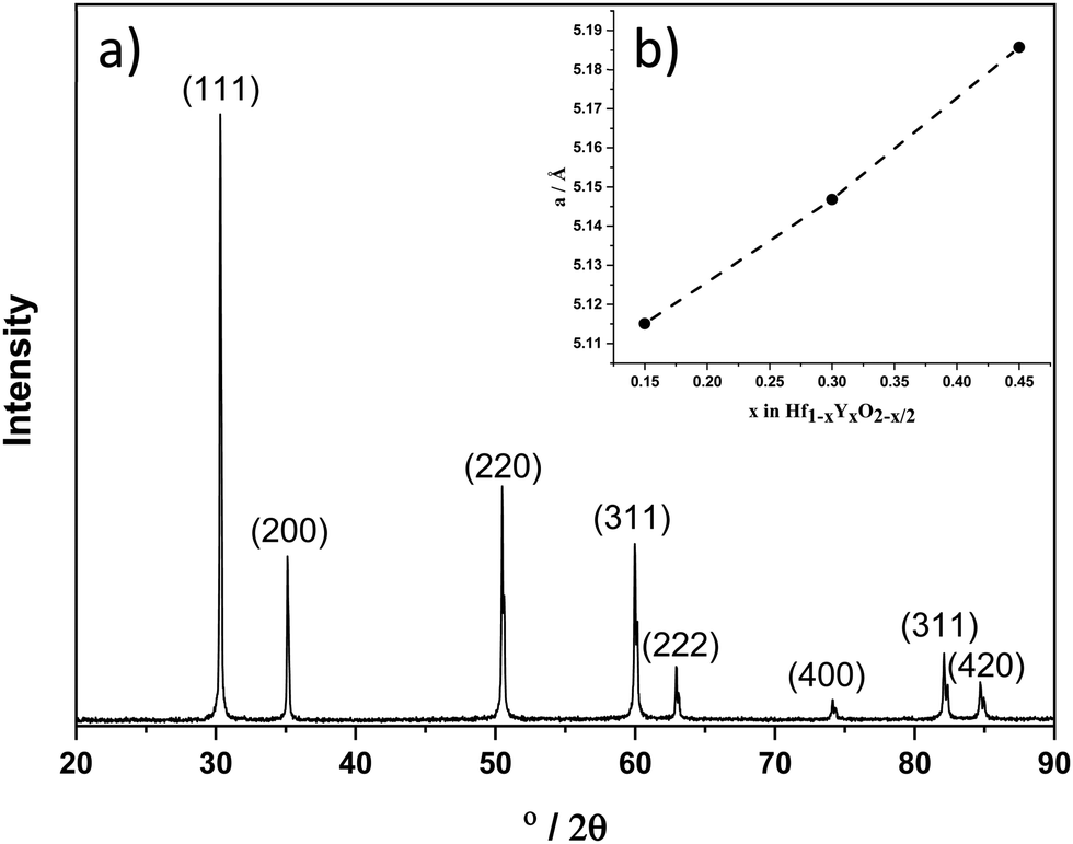 | ||
| Fig. 3 (a) XRD patterns of Hf1−xYxO2−x/2x = 0.15, (b) lattice parameter versus x. | ||
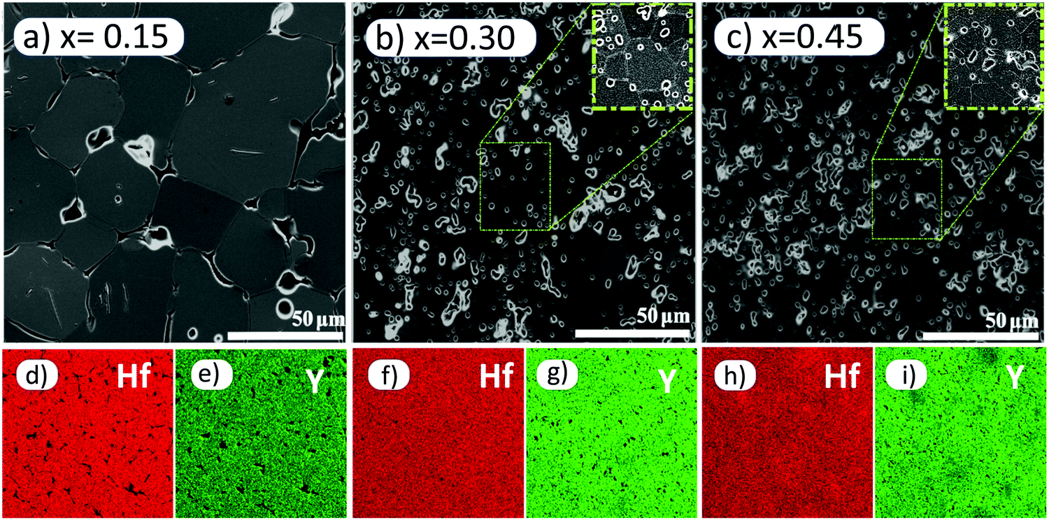 | ||
| Fig. 4 Secondary electron images and EDX maps of polished, thermally etched (a, d and e) x = 0.15, (b, f and g) x = 0.30 and (c, h and i) x = 0.45. | ||
Impedance spectroscopy data
A typical set of impedance data, measured in air at 376 °C and plotted in different formats, is shown in Fig. 5 for a pellet of x = 0.15. A selection of datasets for all three compositions and at different temperatures in the range 275–740 °C, is shown in Fig. S1–S6 (ESI†).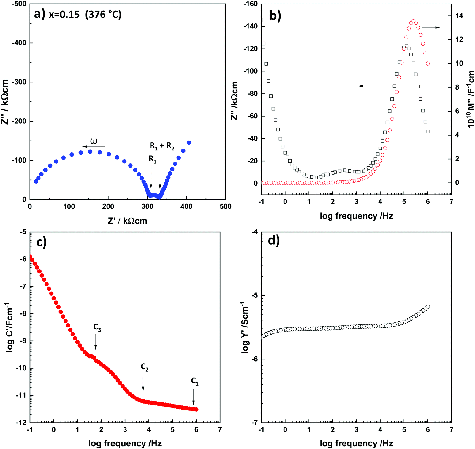 | ||
| Fig. 5 (a) Complex plane plot (Z*) and spectroscopic plots of (b) Z′′/M′′, (c) C′ and (d) Y′ of x = 0.15 in air at 376 °C. | ||
The impedance complex plane plot, Z*, Fig. 5(a), shows two approximately semicircular arcs at high frequencies and a curved inclined spike at low frequencies. A similar response was observed with all compositions at lower temperatures, Fig. S1, S3 and S5 (ESI†). The Z′′/M′′ spectroscopic plots, Fig. 5(b) show peaks at high frequency in Z′′ and M′′ and a small peak at intermediate frequencies in Z′′. The high frequency peaks are approximately Debye-like with full width at half maximum, FWHM, close to the value for a Debye peak of 1.14 decades, and peak maxima at similar frequencies, both of which indicate a good degree of electrical homogeneity in the bulk response.
C′ data, Fig. 5(c), show evidence of a high-frequency plateau, C1, of value ∼2 pF, which corresponds to a permittivity, ε′, value of 22.6 calculated from:
| ε′ = C1/e0 | (4) |
The C′ values increase with decreasing frequency, Fig. 5(c), with some evidence for a poorly-resolved intermediate plateau, C2, at ∼6 pF, corresponding to a permittivity of ∼70. This value is much smaller than expected for a typical grain boundary or surface layer impedance. A similar capacitance has been seen in samples of both yttria- and calcia-stabilised zirconia17,18 and attributed to the presence of dipoles created by oxygen vacancy-yttrium/calcium dopant pairs. These dipoles do not contribute to the long range conductivity but are in evidence in the impedance data at high ac frequencies.
A poorly-resolved, low frequency C′ plateau, C3, is seen at 0.1 nF cm−1 which corresponds to the small, intermediate frequency arc in Z*, Fig. 5(a) and is attributed to a grain boundary impedance. At still lower frequencies, the highest values of C′, ≥ 1 μF, Fig. 5(c) correspond to the low frequency spike in (a) and are attributed to the electrode-sample interface at which oxide ion blocking forms a double-layer capacitance. The curvature of the spike at lowest frequencies Fig. 5(a) indicates that the capacitance is not completely blocking, however, but is in parallel with a resistance that represents a combination of a small amount of electronic conduction through the sample and/or redox processes involved in charge transfer of oxygen across the electrode-sample interfaces. At higher temperatures, especially for x = 0.15, Fig. S2 (ESI†), C′ data show a poorly-resolved plateau around 10 μF but continue to rise to ≥200 μF at 0.1 Hz. In addition, low frequency Z* plots, Fig. S1(d and e) (ESI†) show the emergence of a second arc in the low frequency part of the impedance response which indicates a more complex nature of the sample-electrode interface impedances and probably includes a Warburg diffusion impedance associated with diffusion of O2 molecules through the metal electrode and towards/away from the interfaces.
Y′ data show two overlapping plateaux at intermediate frequency of which the lower frequency plateau corresponds to the total conductivity Fig. 5(d). At high frequencies, the onset of a power law dispersion is seen and is attributed to Jonscher Power Law behaviour which is a common feature of materials that are ionic and/or electronic hopping conductors.
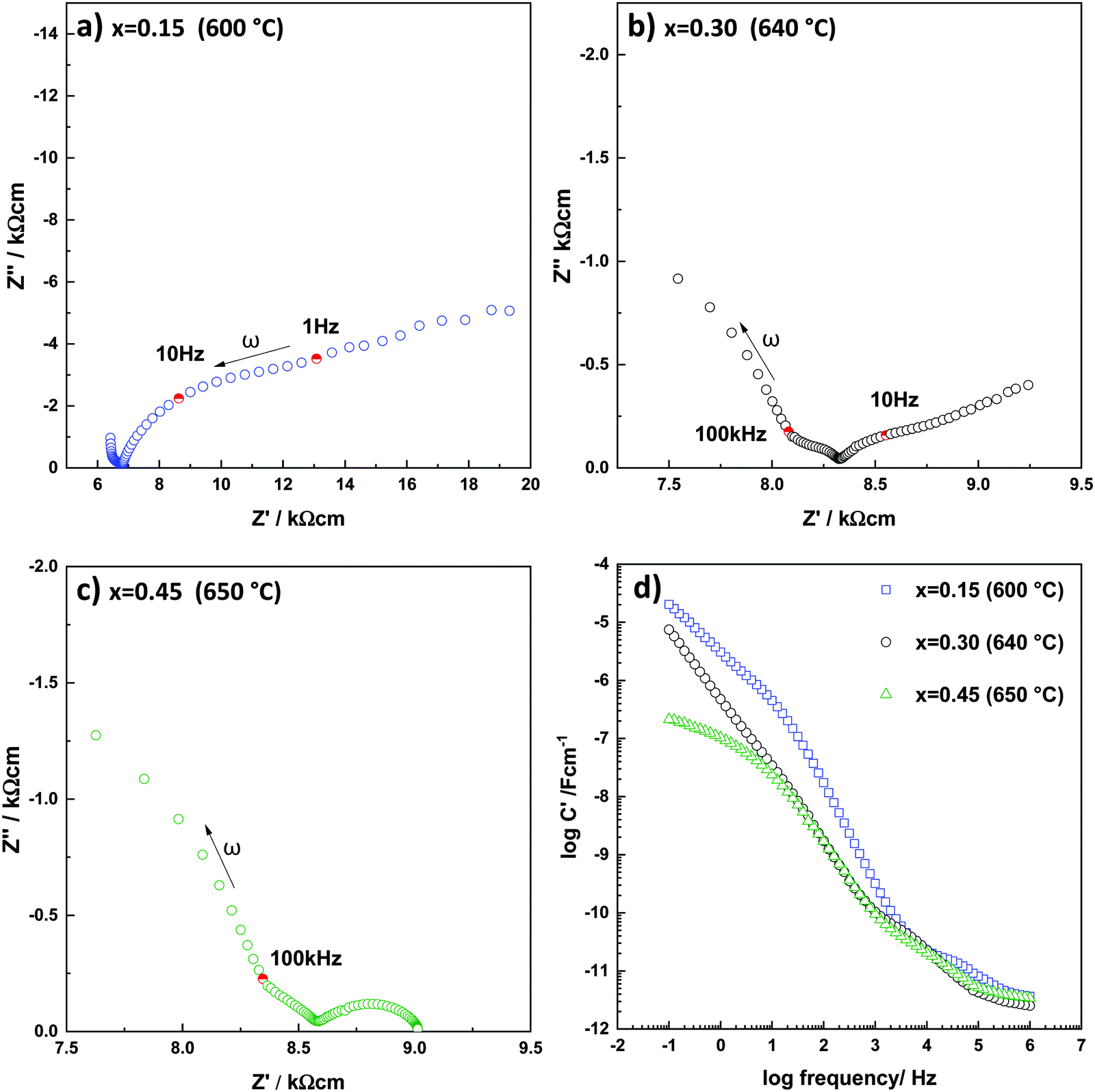
Impedance data of x = 0.30 and 0.45 were similar to those of x = 0.15, but with two key differences, especially at higher temperatures where the low frequency impedance effects are seen more clearly, Fig. 6 and Fig. S3, S5 (ESI†). First, the low frequency spike turned into a small arc for the composition of highest Y3+ content, x = 0.45. This effect was much more noticeable than the changes in curvature seen with x = 0.15. Second, with increasing Y3+ content, capacitance data, Fig. 6(d), show a noticeable reduction in value at low frequencies, indicating that charge transfer at the double-layer interface is no longer predominant. This effect is interpreted as demonstrating the onset of electronic conduction with increasing Y3+ content in YSH and is similar to results reported for YSZ ceramics of high Y content.12
 | ||
| Fig. 6 Complex plane plots (Z*) for (a) x = 0.15, (b) x = 0,30, (c) x = 0.45 and (d) C′ spectroscopic plots, measured in air. | ||
From impedance data such as those shown in Fig. 5 and 6, values for bulk, grain boundary and total conductivities were extracted and are shown as Arrhenius plots in Fig. 7. In all three cases, the grain boundary resistance is much smaller than the bulk resistance and therefore the total conductivities in Fig. 7(a) approximate to the bulk conductivities. x = 0.15 shows a higher conductivity, by ∼1 order of magnitude, than 0.30, 0.45. The Arrhenius plots for bulk and total conductivities of 0.15 are non-linear Fig. 7(a), which is typical behaviour of yttria-stabilized zirconia, shown for YSZ08 in Fig. 7(a) for comparison.19 The total conductivity decreases with x, as has been reported in the literature9 and is attributed to oxide ions, especially for the lower x compositions. However, the similarity in Arrhenius plots of 0.30 and 0.45, Fig. 7(a), may be because the ionic conductivity decreases but electronic conductivity increases with x and the two effects largely cancel to give similar overall conductivities.
 | ||
| Fig. 7 (a) Arrhenius plots of total conductivity of x = 0.15, 0.3 and 0.45 sintered at 1650–1750 °C. Activation energies in eV are shown beside each data set. Data for YSZ08 sintered at 1550 °C for 2 h are included for comparison.19 (b and c) Arrhenius plots of bulk and grain boundary conductivities. Note: the gb data are not corrected for gb geometry. | ||
The grain boundary conductivities appear to be approximately one order of magnitude higher than the bulk conductivities for all three YSH compositions, Fig. 7(b and c). However, in order to obtain true conductivities, they should be corrected for grain boundary geometry as follows. The capacitance, C of a sample or region of a sample is given by:
| C = eoε′Ad−1 | (5) |
The electrical microstructure of the ceramics has, therefore, grain boundary resistivities that are much larger than grain resistivities but, because the grain boundaries are thin, the bulk resistances dominate the overall sample resistances, as shown in the impedance data in Fig. 5(a) and 6(a–c). We note that, for all three compositions, the grain boundary activation energy, Egb is significantly greater than that of the bulk, Eb. The differences in resistivity of the two regions are not simply due to either differences in mobile carrier concentration, or to a constriction resistance model of the grain boundary resistance,20,21 therefore, but involve either a difference in mobility or a contribution from mobile carrier creation. This may be a consequence of small structural or compositional differences between grain interiors and grain boundaries, although there is no evidence of cation segregation from the EDX maps, Fig. 4.
The effect of pO2 on impedance data is shown in Fig. 8 and 9. For all three compositions, it is clear that the bulk resistance is lower in O2 than in N2. This indicates that there is an electronic component of the overall conductivity since the level of oxide ion conductivity should be insensitive to pO2. Further, the reduction in resistance with increasing pO2 is indicative of p-type behaviour since holes are created by absorption and dissociation of oxygen molecules, given ideally as:
 | (6) |
 | ||
| Fig. 8 (a and c) Impedance complex plane plots, (b and d) C′ spectroscopic plots of x = 0.15 measured in dry N2 and O2 at 450 and 503 °C, respectively. Experimental data points and fits to the circuits are shown. | ||
 | ||
| Fig. 9 (a and c) Impedance complex plane plots, (b and d) C′ spectroscopic plots for x = 0.30, x = 0.45 measured in dry N2 and O2 at 554 and 526 °C, respectively showing experimental data and fits. | ||
The electrode contact resistances decrease greatly with increasing pO2, as shown by the decrease in size of the low frequency impedance arc, which reflects the involvement of oxygen molecules in reactions at the sample-electrode interfaces.
In order to obtain accurate resistance values, including for the grain boundary resistance, circuit fitting was carried out as follows. The chosen equivalent circuit that represents the complete range of impedance data is shown in Fig. 8 and 9. It is the same as that proposed by recent accurate modelling of impedance data for YSZ and calcia-stabilized zirconia, CSZ.17,18 Assessment of the validity of the chosen circuit was performed in different ways: (a) visual examination of experimental and fitted data, utilizing the presentation of data in various impedance formalisms, (b) comparison of the fit residuals between experimental and calculated data, (c) examination of the values of the fitted data and their temperature-dependence to determine whether they give realistic values for the electrical property characteristics of the sample.
The proposed circuit, Fig. 8(b and d), is composed of four components. First, a parallel combination of R1, CPE1 and C1 to represent the bulk conductivity response which is also in parallel with C0 and R0 connected in series to model the dipole contribution to the ac conductivity. Second, a parallel combination of R2 and CPE2 that is attributed to the grain boundary impedance. The third and fourth components contain two parallel combinations, R3–CPE3 and R4–CPE4, connected in series to represent the sample-electrode impedance.
It was found that this circuit was a ‘master circuit’, parts of which fitted all the impedance data over a wide range of temperature. Since only a limited range of experimental frequencies was available, (0.1–106 Hz), the master circuit was not needed, or able, to fit all the data at every temperature. Nevertheless, each component in the circuit could be evaluated and component parameters provided for a range of temperatures. Fits are shown Fig. 8, 9 and Fig. S7–S10 (ESI†). The residuals indicate good quality of fits, Fig. S7–S10(d and h) (ESI†). In some cases, the fits are less good at high and low frequencies; this is attributed to the limited amount of data available at these temperatures to obtain accurate fits, as well as inaccuracies in experimental data at the frequency extremes. Fitted resistance values at two temperatures in both N2 and O2 are given in Tables 2 and 3; complete data sets are given in Tables S1 and S2 (ESI†).
| x = 0.15 (451 °C/N2) | x = 0.15 (451 °C/O2) | x = 0.15 (503 °C/N2) | x = 0.15 (503 °C/O2) | |
|---|---|---|---|---|
| R 1 (kΩ cm) | 26.29(5) | 25.09(2) | 7.291(8) | 7.046(6) |
| R 2 (kΩ cm) | 2.04(5) | 1.96(2) | 0.539(9) | 0.506(7) |
| R 3 (kΩ cm) | 450(2) | 77.8(4) | 30(10) | 8.27(6) |
| R 4 (kΩ cm) | — | 63(13) | — | 31(2) |
| x = 0.30 (554 °C/N2) | x = 0.30 (554 °C/O2) | x = 0.45 (526 °C/N2) | x = 0.45 (526 °C/O2) | |
|---|---|---|---|---|
| R 1 (kΩ cm) | 47.40(3) | 45.67(3) | 122.2(1) | 115.4(1) |
| R 2 (kΩ cm) | 1.65(3) | 1.47(4) | 4.6(2) | 6.2(2) |
| R 3 (kΩ cm) | 40(1) | 1.5(1) | 32(1) | 14.2(6) |
| R 4 (kΩ cm) | — | 18(2) | — | — |
Transport number measurements
Results of oxygen transport number measurements are shown for three temperatures in Table 4. The value of ti is slightly less than unity for x = 0.15, decreases with x at 800 °C, consistent with the pO2 dependence of the conductivity data shown in Fig. 8, 9 and Tables 2 and 3 and is attributed to the onset of p-type electronic conduction. x = 0.15 is therefore at the cross-over between the electrolytic and p-type domains under atmospheric conditions. Both R1 and R2 decrease with increasing pO2, Table 2, and therefore, the conductivity Arrhenius plots for x = 0.15, Fig. 7, represent a combination of oxide ion and electronic conductivities. Similar effects are seen with x = 0.30, 0.45; the low frequency impedance data also show increasing evidence of electronic conductivity, especially for x = 0.45. We are unable to comment on the relative activation energies of oxide ion and electronic conduction. As far as we can tell, the two mechanisms of ionic and electronic conduction are entirely independent of each other. Transport measurements are likely to be influenced by ceramic microstructure, which may affect the amount of atmospheric oxygen that can be exchanged with the samples, as well as the different resistances that contribute to the overall electrical properties. We regard the data in Table 4 as indicative rather than quantitative, therefore.| Composition | t ion (600 °C) | t ion (700 °C) | t ion (800 °C) |
|---|---|---|---|
| x = 0.15 | 0.86 | 0.94 | 0.99 |
| x = 0.30 | 0.79 | 0.78 | 0.92 |
| x = 0.45 | 0.93 | 0.88 | 0.85 |
Discussion
YSH materials with a fluorite structure are majority oxide ion conductors with a small amount of p-type conductivity that is very dependent on atmosphere. Of the three compositions studied here, the oxide ion conductivity is greatest for x = 0.15, similar to that reported previously.9 The decrease in oxide ion conductivity at higher Y3+ contents is similar to that seen with YSZ compositions, which is attributed to increased trapping of the mobile oxide ion carriers in defect complexes.6,12,22,23The onset of p-type conductivity with increasing Y3+ content is also similar to that seen with YSZ compositions.12 The location of the holes in both systems is almost certainly on oxygen since the possibility of impurities such as Fe being present in both systems and to an extent that depends on Y3+ content, is most improbable. In addition, location of holes on Y or Hf, to take them above their usual charge states of Y3+ and Hf4+, is most unlikely.
As proposed previously,11,12 holes appear to be located on under-bonded oxide ions that are surrounded by insufficient positive charge to fully stabilize the O2− ion in the crystal lattice. Such under-bonded oxide ions in the bulk region are associated with the acceptor dopants, in this case Y3+, which substitutes for Hf4+. Charge compensation for the acceptor dopants involves creation of oxygen vacancies and these are able to absorb oxygen molecules from the surrounding atmosphere, thereby providing the mechanism for hole creation, eqn (6). Additionally, at sample surfaces and interfaces such as grain boundaries, oxide ions may be under-bonded due to an incomplete coordination arrangement of surrounding cations. Some of the oxide ions, in both bulk and grain boundary regions, may ionise spontaneously giving rise to hole conductivity. They may also ionise easily in response to an increase in pO2,12eqn (6), or, as described in other systems, to the application of a dc bias.11,24,25
These results raise an interesting question as to the intrinsic stoichiometry of materials such as YSH and YSZ since their oxygen content is variable, albeit by a small amount, depending on the atmospheric conditions. Oxygen non-stoichiometry in transition metal oxides is of course, commonplace and is associated with mixed oxidation states of the metal component. In the present case, by contrast, oxygen is the element that potentially, has a mixed oxidation state. These materials exhibit hopping, p-type semiconductivity and the only realistic location of holes is on oxygen since the cations that are present are already in their highest valence states, i.e. Hf4+, Zr4+ and Y3+; in addition, the holes are not delocalised in a band structure. The possibility of redox-active oxygen in oxides has not been considered seriously by most within the electroceramics and chemistry communities until the recent discoveries of battery charge/discharge mechanisms in certain Na and Li transition metal oxide cathodes for which the observed capacities could not be attributed to the transition metal component alone. Nowadays, there are many examples cited of anion redox activity in battery systems.26,27
The present materials have O2− ions as their principal anions but a small amount of O− ions can be created by reaction with atmospheric oxygen leading to oxygen redox activity. The unavoidable conclusion, therefore, is that oxygen in oxides should not be regarded always as an inert packing anion but, in certain circumstances, it can be redox active. The classic ionic oxide Al2O3, provides a recent example of p-type conductivity that was also attributed to redox-active oxygen.28
Conclusions
The ac impedance results of Hf1−xYxO2−x/2 (YSH, x = 0.15, 0.30 and 0.45) demonstrate clear evidence of oxide ion conduction with an inclined Warburg spike at low frequency and a capacitance value of ≥10−6 F cm−1. Composition x = 0.15 had a conductivity that was ∼1 order of magnitude higher than that of x = 0.30 and 0.45. The materials are foremost oxide ion conductors but with increasing pO2 become p-type mixed conductors. The increase in conductivity with increasing pO2 is reversible and is attributed to oxygen absorption in the vacancies that are created by charge compensation on substituting Hf4+ by Y3+ together with the creation of holes on under-bonded oxide ions. The p-type semiconductivity is in parallel with the pre-existing oxide ion conduction. The YSH materials at high temperatures in air are, therefore, located just beyond the high pO2 limits of the electrolytic domain. They represent the second known example of this effect in the family of stable, fluorite-based oxide ion conductors in which hole location on oxygen is responsible for the p-type behaviour and represent a practical limit on the possible application of such materials as solid electrolytes. The possibility of cross-over between electrolytic and p-type domains is well-recognised in the literature on oxides, but its origin, and especially the location of holes, has been discussed rarely, in contrast to the widely-studied onset of n-type behaviour that is observed at low pO2 and associated with oxygen loss.Conflicts of interest
There are no conflicts to declare.Acknowledgements
Meshari Alotaibi acknowledges financial support through Taif University, Saudi Arabia. We thank Le Ma for the SEM/EDX results.References
- P. Hagenmuller and W. Van Gool, Solid electrolytes: general principles, characterization, materials, applications, Elsevier, 2015 Search PubMed.
- T. Etsell and S. N. Flengas, Chem. Rev., 1970, 70, 339–376 CrossRef CAS.
- S. C. Singhal and K. Kendall, High-temperature solid oxide fuel cells: fundamentals, design and applications, Elsevier, 2003 Search PubMed.
- H. Tuller, Springer Handb. Electron. Photonic Mater., 2017, 1 Search PubMed.
- A. R. West, Solid state chemistry and its applications, John Wiley & Sons, 2014 Search PubMed.
- S. T. Norberg, S. Hull, I. Ahmed, S. G. Eriksson, D. Marrocchelli, P. A. Madden, P. Li and J. T. Irvine, Chem. Mater., 2011, 23, 1356–1364 CrossRef CAS.
- V. Kharton, F. Marques and A. Atkinson, Solid State Ionics, 2004, 174, 135–149 CrossRef CAS.
- M. F. Trubelja and V. S. Stubican, J. Am. Ceram. Soc., 1991, 74, 2489–2494 CrossRef CAS.
- J. D. Schieltz, Doctor of Philosophy Dissertation, Iowa State University, 1970 Search PubMed.
- H. Johansen and J. Cleary, J. Electrochem. Soc., 1964, 111, 100–103 CrossRef CAS.
- N. Masó and A. R. West, Chem. Mater., 2015, 27, 1552–1558 CrossRef.
- M. Jovaní, H. Beltrán-Mir, E. Cordoncillo and A. R. West, Inorg. Chem., 2017, 56, 7081–7088 CrossRef PubMed.
- M. Guo, N. Masó, Y. Liu and A. R. West, Inorg. Chem., 2018, 57, 64–71 CrossRef CAS.
- N. Masó, H. Beltrán, M. Prades, E. Cordoncillo and A. R. West, Phys. Chem. Chem. Phys., 2014, 16, 19408–19416 RSC.
- J.-L. Courouau, J. Fouletier and M. Steil, Electrochim. Acta, 2020, 331, 135269 CrossRef CAS.
- A. Weyl and D. Janke, J. Am. Ceram. Soc., 1996, 79, 2145–2155 CrossRef CAS.
- X. Vendrell and A. R. West, J. Electrochem. Soc., 2018, 165, F966–F975 CrossRef CAS.
- J. Ramírez-González and A. R. West, J. Eur. Ceram. Soc., 2020, 40, 5602–5611 CrossRef.
- X. Vendrell, D. Yadav, R. Raj and A. R. West, J. Eur. Ceram. Soc., 2019, 39, 1352–1358 CrossRef CAS.
- P. G. Bruce and A. West, J. Electrochem. Soc., 1983, 130, 662 CrossRef CAS.
- Y. Li, M. Liu, J. Gong, Y. Chen, Z. Tang and Z. Zhang, Mater. Sci. Eng., B, 2003, 103, 108–114 CrossRef.
- D. Marrocchelli, P. A. Madden, S. T. Norberg and S. Hull, Chem. Mater., 2011, 23, 1365–1373 CrossRef CAS.
- Y. Arachi, H. Sakai, O. Yamamoto, Y. Takeda and N. Imanishi, Solid State Ionics, 1999, 121, 133–139 CrossRef CAS.
- X. Vendrell and A. R. West, J. Am. Ceram. Soc., 2019, 102, 6100–6106 CrossRef CAS.
- M. Prades, N. Masó, H. Beltrán, E. Cordoncillo and A. R. West, J. Mater. Chem., 2010, 20, 5335–5344 RSC.
- M. Okubo and A. Yamada, ACS Appl. Mater. Interfaces, 2017, 9, 36463–36472 CrossRef CAS.
- T. Sudayama, K. Uehara, T. Mukai, D. Asakura, X.-M. Shi, A. Tsuchimoto, B. M. de Boisse, T. Shimada, E. Watanabe and Y. Harada, Energy Environ. Sci., 2020, 13, 1492–1500 RSC.
- J. Ramírez-González and A. R. West, J. Eur. Ceram. Soc., 2021, 41, 3512–3519 CrossRef.
Footnote |
| † Electronic supplementary information (ESI) available. See DOI: 10.1039/d1cp04642j |
| This journal is © the Owner Societies 2021 |