
 Open Access Article
 This Open Access Article is licensed under a
 Creative Commons Attribution 3.0 Unported Licence
Chemistry of the photoisomerization and thermal reset of nitro-spiropyran and merocyanine molecules on the channel of the MoS2 field effect transistor†
Muhammad Shamim Al
Mamun
 a,
Yasuyuki
Sainoo
b,
Tsuyoshi
Takaoka
b,
Hiroki
Waizumi
a,
Zhipeng
Wang
a,
Md Iftekharul
Alam
a,
Atsushi
Ando
c,
Ryuichi
Arafune
d and
Tadahiro
Komeda
*b
a,
Yasuyuki
Sainoo
b,
Tsuyoshi
Takaoka
b,
Hiroki
Waizumi
a,
Zhipeng
Wang
a,
Md Iftekharul
Alam
a,
Atsushi
Ando
c,
Ryuichi
Arafune
d and
Tadahiro
Komeda
*b
aDepartment of Chemistry, Graduate School of Science, Tohoku University, Aramaki-Aza-Aoba, Aoba-Ku, Sendai 9808578, Japan. E-mail: tadahiro.komeda.a1@tohoku.ac.jp
bInstitute of Multidisciplinary Research for Advanced Materials (IMRAM, Tagen), Tohoku University, 2-1-1, Katahira, Aoba-Ku, Sendai 9800877, Japan
cNational Institute of Advanced Industrial Science and Technology, 1-1-1 Umezono, Tsukuba, Ibaraki 305-8568, Japan
dInternational Center for Materials Nanoarchitectonics (WPI-MANA), National Institute for Materials Science (NIMS), Tsukuba, Ibaraki 304-0044, Japan
First published on 15th November 2021
Abstract
We have explored the chemical reaction of the photoisomerization and thermal reaction of the photochromic spiropyran (SP) 1′,3′-Dihydro-1′,3′,3′ trimethyl-6-nitrospiro[2H-1 benzopyran-2,2′-(2H)-indole] molecule deposited on the atomic thin channel of a MoS2 field-effect transistor (FET) through the analysis of the FET property. With four monolayers of SP molecules on the channel, we observed a clear shift of the threshold voltage in the drain-current vs gate-voltage plot with UV-light injection on the molecule, which was due to the change of the SP molecule to merocyanine (MC). A complete reset from MC to SP molecule was achieved by thermal annealing, while the injection of green light could revert the FET property to the original condition. In the process of change from MC to SP, two types of decay rates were confirmed. The quick- and slow-decay components corresponded to the molecules attached directly to the substrate and those in the upper layer, respectively. The activation energies for the conversion of MC to SP molecules were estimated as 71 kJ/mol and 90 kJ/mol for the former and latter, respectively. Combined with DFT calculations, we concluded that the Id-Vg shift with photoisomerization from SP to MC is due to the upper layer molecules and the dipole moment in the surface normal direction. Based on the estimated activation energy of 90 kJ/mol for the reset process, we calculated the conversion rate in a controllable temperature range. From these values, we consider that the chemical state of MC can be maintained and switched in a designated time period, which demonstrates the possibility of this system in logical operation applications.
Introduction
Much attention has been paid to functional molecules that can switch properties with external stimulation in the development of materials for optical sensors and more complex optical information processing.1 For such applications, it is critical to developing a method to amplify the molecular changes to a detectable physical property. Since most of the crystals of those functional molecules have low electrical conductance, it might be good to combine the molecules with the channel of a field-effect transistor (FET) and detect the variations in the target molecule properties by the changes in the FET properties in an indirect manner. For such applications, the use of FET with atomic thin, two-dimensional (2D) channel materials has an advantage in terms of sensitivity. This is because the channel of such a FET has a large surface-to-volume ratio and the change in the properties of the topmost layer affects the FET property sensitively.The family of photochromic molecules is a good candidate for applications, such as optical sensors and information processing with the use of the light.2–5 Various compounds, including hydrazines,6,7 indigos,8 semicarbazones,9 dihydropyrenes,10 o-nitrobenzyl derivatives,11 azobenzenes12,13 and spiropyrans (1′,3′-dihydro-1′,3′,3′-trimethyl-6-nitrospiro[2H-1-benzopyran-2,2′-(2H)-indole], abbreviated as SP hereafter)14 have been explored.
Especially, the SP molecule and its derivatives are well studied, and the mechanism of switching with light in the solution phase is well-examined.15–18 The SP molecule shows a ring-opening reaction with UV-light exposure to form merocyanine (MC), which is energetically unstable compared with the SP molecule. It can be reversed to the initial SP molecule by visible-light irradiation or thermal activation. However, it is well-known that functional molecules, when adsorbed on the surfaces of metals and semiconductors, modify their behavior in response to external stimuli. It is either due to the change in the chemical properties of the molecule due to adsorption on the substrate19 or due to electron–hole pair creation in the substrate, which accelerates the quenching of the excited state of the molecule.20 It is very well known that changes of in environment between the solution and gas/vacuum affect photoisomerization. It has been actually demonstrated that, when deposited on an Au substrate, the SP molecule becomes energetically less stable than the MC molecule, contrary to the behavior in solution.19 It is claimed that the in flat-lying adsorption configuration, the MC molecule forms a stronger interaction with the Au substrate and comes to the ground state. Due to this reversal in the energy levels, if once an SP molecule is thermally converted into an MC molecule on the Au substrate, it cannot be reverted to the SP form.19
In this report, by fabricating a FET device using an atomic thin MoS2 layer as the channel and depositing the SP on the channel, we explore the chemical change of the SP molecule via the photoisomerization and a thermal reaction by monitoring the FET properties. The photoisomerization of several photochromic molecules in combination with FET devices made of 2D-material channels have been reported, including graphene and SP,21,22 MoS2 channel and an SP-derivative bearing an 18-carbon-long alkyl chain,23 and WSe2 channel with silane-terminated SP.24 In these cases, the overall FET behavior was explained along with the photochromic behaviors of the molecules examined in solution. A recent report showed that a FET with the atomic layer channel has the sensitivity to reveal the formation of a self-assembled layer of SP molecules.25 However, none of these reports reveal the details of the chemical reaction on the transition metal dichalcogenides, including the energy barrier for the change between SP and MC. This information is indispensable for the precise control of the switching of molecules applied in optical devices.
We successfully detected the changes in the FET property accompanying the switch between SP and MC when a 4 monolayer (ML) SP film was deposited by the drop-cast method. Such a change in drain current vs. gate voltage was absent for the monolayer film formed by the sublimation method. In the case of the 4 ML film, the reverse reaction from MC to SP was successfully achieved by thermal annealing, but the injection of green light could not complete the reset. Two types of decay rates were confirmed. The quick- and slow-decay components corresponded with the molecules attached directly to the substrate (activation energy for MC-SP conversion was 71 kJ mol−1) and those in the upper layer (90 kJ mol−1). Combined with DFT calculations, we concluded that the Id–Vg shift with the photoisomerization from SP to MC is due to the upper layer molecules and the dipole moment in the surface normal direction.
Results and discussion
We fabricated a FET device with a channel composed of four layers of MoS2. The method for the determination of the MoS2 layer thickness has been reported in our previous works.26–28 The deposition of SP molecules on the channel and the electrical measurements were done both in the ambient and vacuum conditions. The latter system was studied in our previous report.26 For both processes, we first confirmed the FET property of the devices used in the photoisomerization experiment. All the Id–Vg measurements were executed at a fixed drain–source voltage of Vds = 50 mV. We deposited the SP molecules by two methods: from the solution and by vacuum sublimation.We first discuss the SP molecule obtained by the solution-transfer method. Electrical measurements with light injection and thermal treatment were executed in an N2 ambient condition. In Fig. 1, the Id–Vg plots for the channels of pristine MoS2 and MoS2 covered with 4 ML of SP molecules, and their variations with photoisomerization are illustrated. For the process of cycling between the SP and MC molecules, we injected UV light for 90 s to convert the SP molecule to MC molecule and injected green light for 8 min to make the MC molecule revert to the SP molecule. This cyclic scheme is named Method 1 and is illustrated in Fig. 1(a). The actual transfer of the SP molecule onto the MoS2 channel surface was confirmed by the Raman spectrum shown in the mapping images of the time-of-flight secondary-ion-mass-spectroscopy (ToF-SIMS) in the ESI.†
 | ||
| Fig. 1 (a) Schematic illustration of Method 1 of cycling the SP and MC molecules with UV and green light. (b) Id–Vg variations the channel from pristine MoS2 with SP deposition and after the cycles of method 1 shown in (a). 4 ML of SP molecule are formed on the MoS2 channel from a solution. (c) Summary of Vth variation with the process shown in (b). | ||
The Id–Vg changes are summarized in Fig. 1(b); the measurement was started from the pristine MoS2 channel, followed by the channel with 4 ML SP molecules deposited (denoted as 'SP') and then with repeated cycles of UV and green light injection. The Id–Vg curve shifted towards the left from the plot of 'SP'. The photoisomerization of SP molecules in solution indicates the conversion of SP to MC molecules.15–18 The direction of the Id–Vg shift is the same as that reported for the SP derivatives.23 This suggests either n-type doping or an effective positive bias was provided by the conversion of SP to MC by UV light irradiation.
We expected the Id–Vg curve to return to the plot of ‘SP’ with green-light irradiation. However, the Id–Vg curve did not revert to ‘SP’ in terms of amplitude or shape. At the end of the third cycle, the Id was at Vg = 30 V, which is smaller than that of ‘SP’, but at Vg < 20 V, the reverse was observed. This meant that, instead of reverting to the SP state, MC had changed to a different species after green light injection.
The incomplete reversal between the SP and MC states in Method 1 was also indicated by the threshold voltage (Vth) of the Id–Vg curve at which the increase in drain current started. The method to determine the Vth is described in the ESI.† The results of the three cycles are illustrated in Fig. 1(c). The Vth values changed sporadically, and the values after green light injection did not return to that of the ‘SP’ state. This would cause a large problem in sensors and other electric devices since resetting to the original state of SP is a mandatory process in such applications.
In order to search for a method to achieve the complete reset of the MC molecule to SP, we explored Method 2 depicted in Fig. 2(a), in which the reaction from MC to SP was carried out by a thermal process. Each cycle involved UV irradiation followed by thermal annealing at 80 °C for 3 min. The Id–Vg curve was obtained at the end of each cycle and summarized in Fig. 2(b). In contrast to the use of the green light, the Id completely returned to the starting position of the SP molecule in this case. This demonstrates that the molecule was reset to the SP state successfully by using the thermal annealing process. There was a small deviation from the original plot for MC in the third cycle. This might be caused because the sample in the device was not fully cooled to RT, with the shape resembling that obtained at higher temperatures.
 | ||
| Fig. 2 (a) Method 2 of cycling the SP and MC molecules with UV and heating. (b) Id–Vg variations of the pristine MoS2 channel with SP deposition and after the cycles of method 2. (c) Summary of the Vth variation with the process shown in (b). | ||
The drain current at the same gate voltage of 20 V was higher in Method 2 than that obtained with Method 1. This is mainly caused by the difference in the FET properties of the pristine devices used in Methods 1 and 2. The origin of the fluctuation in the threshold voltage between the devices is mainly the change in contact resistance between the highly doped Si (back gate) and the gate electrode. It was confirmed that the ON/Off ratios were comparable for the two devices.
The good reproducibility of the switch between the SP and MC states with the use of Method 2 can also be seen in the Vth plot shown in Fig. 2(c). Compared with the results of Method 1 illustrated in Fig. 1(c), the values after each process agreed well with each other. It should be noted that, after all the heating processes, the Vth returned to the value of ‘SP’.
Then, we examined the dynamics of conversion from MC to SP by measuring the time-dependent change in drain current. In Fig. 3(a), we show the time-dependent variation in the Id–Vg curve with UV light illumination on the channel and when it was kept in the dark condition. After the initial shift of the Id–Vg curve towards the left under UV irradiation, it showed slow relaxation towards the original curve with time in the dark condition.
 | ||
| Fig. 3 (a) Transfer characteristics at room temperature: SP-covered surface without (black line) and after UV irradiation (red) and when kept in the dark for 1 min (blue), 2 min (green) and 3 min (violet). (b) Drain current as a function of time: UV irradiation at 5 s time intervals. (c) Drain current as a function of time: UV irradiation for 1 s. (d) Decay in drain current after UV light injection on the SP covered and pristine MoS2 channels. The red line is the fitting result with the exponential decay function. | ||
In Fig. 3(b), we show the change in drain current versus time with the injection of UV light for 5 s followed by relaxation in the dark. The time periods of UV light irradiation are colored yellow. The Id values were obtained with the gate voltage of Vg = −55 V, which was chosen so that the change in drain current is most clearly observed in the sub-threshold region.
The drain current increased quickly after the start of UV irradiation followed by a slower increase rate that continued until the light was stopped. On turning off the UV irradiation, the drain current dropped quickly in the initial stage followed by slow decay. For example, at 10 s, when the first injection was stopped, the current dropped by 30% within 1 s and then decreased slightly until the time of 15 s, when the light was injected again. As the cycles of ON/OFF of the UV light were repeated, the increase/decrease of the drain current became smaller, and the drain current seemed to be saturated at some point.
The drain current variation over a time span is shown in Fig. 3(c), which was obtained at a fixed gate voltage of −20 V and a shorter UV irradiation pulse of ∼1 s. Again, Id showed a sharp drop after the UV pulse irradiation (at 10 and 20 s) followed by slow decay.
It has been shown that the SP state is energetically more stable than the MC state in solution.17 Even with the presence of the activation barrier, the converted MC state can be thermally relaxed to the SP state. This apparently corresponds to the component marked as ‘slow decay’ in Fig. 3(c), which reached the condition before UV light irradiation with a relaxation time of one hour. Besides this slow component, we can see another component that decays in less than one second.
First, we estimated the activation barriers of both the quick- and slow-decay components. The Idvs. t curve could be fitted using the following exponential function.
y = A1![[thin space (1/6-em)]](https://www.rsc.org/images/entities/char_2009.gif) exp(−k·t) + y0 exp(−k·t) + y0 | (1) |
The experimental data and the fitting curve are shown as black dots and the red line in Fig. 3(d), respectively. For comparison, we have shown the data obtained for pristine MoS2 as small blue squares. Although both the SP-covered and pristine cases started from 20 pA, the increase in drain current after UV light injection showed a large difference; the values increased by 10 and 80 pA for the pristine and SP-covered surfaces, respectively. They also showed a significant difference in the decay rate. The photocurrent induced by light irradiation on the pristine MoS2 surface has been investigated in many reports since it can be applied to optical devices. Due to the change in the band structure with the conversion from bulk to an atomic thin layer, direct band transition occurs.29 When the bandgap energy is close to that of visible green light, and a large photocurrent appears with the incidence of light close to 600 nm.30–32 However, the photocurrent generated with the UV light was small in this case, which is the reason for the small current increase of 10 pA with UV irradiation.
In the time range shown in Fig. 3(d), the quick-decay component dominates. Thus, we considered a single component. The decay constant, τ = 1/k was found to be ∼0.7 s for the SP-covered surface, while it was ∼0.1 s for the pristine case, showing a large difference in the decay time between the two. Combined with the small contribution of the photocurrent generated with UV light irradiation, we judged that the quick-decay component observed for the SP-covered surface was not derived from the photocurrent effect of the MoS2 substrate.
Next, we examined the decay constant of the slow-decay component. Since the decay was slow, we could measure the variation of the Id–Vg curve with time. This gave more information than simple monitoring of the drain current at a fixed gate voltage. We derived the threshold voltage of each curve.
The 4 ML film of SP molecules formed on the channel by the drop-cast method was converted to MC molecules using the UV light, and the Id–Vg plots were taken at 30 s intervals up to 180 s at the temperature of 298.2 K. The calculated Vth at each time point is illustrated in Fig. 4(a). In addition, in order to determine the activation energy of this component, we examined the change in Vth with time at different temperatures, as shown in Fig. 4(b)–(f), which correspond to the temperatures 313.2, 323.2, 333.2, 343.15 and 353.2 K.
 | ||
| Fig. 4 Threshold voltage (Vth) as a function of time at different temperatures to determine the conversion rate: (a) 298.15 K; (b) 313.15 K; (c) 323.15 K; (d) 333.15 K; (e) 343.15 K; (f) 353.15 K; (g) the lnk vs. 1/T plot to estimate the activation barrier for MC to convert to SP. | ||
From the plots in Fig. 4(a)–(f), we see that the conversion rate from MC to SP was accelerated with temperature. The details of curve fitting are presented in ESI.†
Fig. 4(g) shows the ln(k) vs. 1/T plot. We considered the Arrhenius relationship as follows:
 | (2) |
We considered these activation energies in the energy diagram for the conversion between the SP to MC molecules. It has been reported that for the SP-MC conversion in solution, the MC molecule in the trans-MC state is converted into the SP molecule through a cis-MC transition state as illustrated in Fig. 5,33 which was confirmed by ultra-fast optical measurements. Thus, the activation energy for conversion from MC to SP should be the energy difference between the trans- and cis-MC states. It has also been reported that isomerization takes place with a dihedral angle rearrangement by conquering steric hindrance for the configuration change.33 In this process, the dihedral angles are rotated as follows: α 180 → 90, β 180 → 0, and γ 180 → 0. The rotations are schematically illustrated in Fig. 5 by arrows.
 | ||
| Fig. 5 Potential energy diagram for the conversion of MC to SP on the MoS2 surface. | ||
These barriers appeared as activation energies in our experiment, which were measured as 71.5 kJ mol−1 and 90.0 kJ mol−1 for the rapid-decay and slow-decay components, respectively.
In order to investigate the molecules that contribute to the rapid- and slow-decay components, we examined the behavior of the monolayer film. It was critical to control the thickness of the film for this purpose, and vacuum sublimation was employed as it is suitable for the precise control of thickness in the sub-monolayer region. Thus, we switched to the experiment in a vacuum condition.
In Fig. 6(a), we compare the Id–Vg plots of the SP film deposited by the sublimation method before and after UV light irradiation. The thickness of the deposited SP film was calibrated by QCM measurements and was controlled to 1 ML. The shift of the curve of MC formed after UV irradiation for 40 min from that of deposited SP was much smaller compared with the shift observed for the 4 ML film transferred from a solution.
 | ||
| Fig. 6 (a) Id–Vg plot for the monolayer film of SP molecules transferred onto the MoS2 channel by the vacuum sublimation method before and after UV light radiation, along with the curve for the pristine MoS2 channel. (b) Comparison of the decay in drain current after UV irradiation on 4 ML and 1 ML SP-deposited channels. | ||
The small shift of the Id–Vg curve observed for the monolayer SP film can be explained by a model in which the MC molecule formed by UV light irradiation is thermally converted into the SP molecule quicker than the measurement time of Id–Vg (∼30 s).
This is demonstrated in Fig. 6(b), which compares the decay of the drain currents of the 1 ML film prepared by vacuum sublimation and the 4 ML film prepared by the drop-cast method. The latter is identical to that shown in Fig. 3(d). The time t = 0 is the moment when we stopped the UV-light injection. The plots have been calibrated so that the maximum drain current at t = 0 s is identical. We see a much quicker decrease in the drain current in the 1 ML case. It is to be noted that the same type of FET has enough sensitivity to show a large Id–Vg shift in the sub-monolayer region,26,28,34 and the small shift in Vth was not derived from the small thickness of 1 ML.
The difference in the decay rates seen in the drain–current plots of Fig. 6(b) can be explained by the following model: two components with rapid- and slow-decay rates are derived from the molecules directly attached to the substrate and those in the upper layer, respectively. As stated above, the interaction between the SP/MC molecules and the substrate have a large effect on the energy positions of the two molecules on the surface of Au.19 We consider that the molecule attached to the substrate is responsible for the rapid-decay component, while the upper layer molecules contribute to the slow-decay component. This is consistent with the behavior in Fig. 6(b), which shows a rapid decrease in the current of the 1 ML film that has a majority of the molecules attached directly to the substrate. The existence of two types of decay constants for conversion from MC to SP molecule has also been reported for SP molecules deposited on graphene channel.21 In that case, the rapid-decay component was attributed to the isolated molecules and the slow-decay component to the molecules in an assembly.
Interestingly, the activation energy of the MC molecule directly attached to the Bi (111) surface in a monolayer is estimated as 79 kJ mol−1,35 which is similar to the energy we estimated for the MC monolayer. These are similar to or slightly higher than those reported for polar solvents like ethanol (75 kJ mol−1)17 and less polar solvents, such as methylcyclohexane (65 kJ mol−1).17
The role of adsorption in changing the activation barrier between the cis- and trans-butene isomers has been reported.36 Thus, we can speculate that lowering the activation barrier between the cis- and trans-MC isomers can be achieved in the presence of the substrate. However, we need further detailed studies to prove this hypothesis.
At the same time, we consider that the shift of the Id–Vg curve with SP to the MC conversion seen in Fig. 2 is derived from the contribution of the upper layer rather than that of the monolayer since the latter does not contribute to Id–Vg.
In the mechanism of the Id–Vg shift due to the adsorbed molecules on the channel, two major processes can be considered. One is the charge transfer between the molecule and the substrate. The electron donated from the molecule to the substrate is expected to contribute to n-type doping. The other is the polarization of the adsorbates, which causes the shift in the gate voltage. However, we had to examine these two effects by comparing the monolayer and upper layers.
We examined the mechanism that caused the shift of Id–Vg in the 4 ML films. For this purpose, it was mandatory to understand the effect of the substrate and compare the monolayer and multilayer. We executed DFT calculations using the VASP code to deduce the most stable bonding configuration for both SP and MC molecules on the MoS2 surface, followed by the estimation of charge transfer and the polarization of the molecules.
We calculated the adsorption energy for the possible adsorption geometries and decided the energetically stable configurations of both SP and MC molecules adsorbed on the MoS2 substrate. It is expected that multiple bonding configurations would exist in the assembly of SP molecules formed by the drop-cast method. Thus, the calculation of the various local minima of the bonding configurations was performed. We evaluated a total of 21 models for the SP and MC bonding configurations, which are shown in the ESI.†
The optimized structures, which represent the local minima, are illustrated in the ESI† together with the total energy of the substrate and the molecule. The most stable configurations for the adsorption of the SP and MC molecules are illustrated in Fig. 7(a) and (b), respectively. We noticed that, even though the MC molecule was stable in a flat-lying structure, the SP molecule showed a complex 3D structure. This was due to the open-ring structure of the MC molecule, which is more flexible than the SP molecule with a closed ring. Due to its flexible nature, the MC molecule could make a flat-lying configuration so as to have stronger bonding with the substrate. Actually, the total energy difference between the SP and MC molecule systems was calculated as 49.4 meV. This value can be converted to 4.8 kJ mol−1, which is almost one order of magnitude smaller than the energy difference between the two in the vacuum, which was estimated as 41.0 kJ mol−1.33
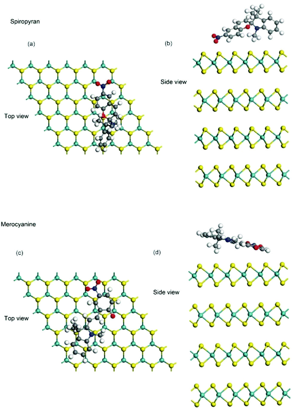 | ||
| Fig. 7 Top panel – optimized model of spiropyran adsorbed on the MoS2 channel: (a) side view and (b) top view. Bottom panel – optimized model of merocyanine adsorbed on the MoS2 channel: (a) side view and (b) top view. | ||
After determining the most stable bonding configurations, we estimated molecular polarization by local potential estimation. The work functions were calculated as 4.95 and 5.18 eV for SP and MC molecule adsorption, respectively. The difference is understood to arise from the flat-lying configuration of the MC molecule. Even though the MC molecule has a larger dipole moment than the SP molecule,23 the polarization of the MC molecule was nearly perpendicular to the surface normal direction. Thus, the contribution of the dipole moment of the MC molecules in the monolayer film is smaller. On the upper layers, the flat-lying configuration cannot gain energy by making bonds with the substrate. Thus, the MC molecules change to an up-right configuration in the upper layer and contribute to more polarization in the surface normal direction. This can be the cause of the larger shift in Vth seen in Fig. 2.
We further calculated the charge transfer between the first-layer molecules and the substrate by Bader analysis. The Bader method estimates the charge distribution estimated by decomposing the molecular charge into contributions from individual atoms by dividing the space within the molecular system into atomic (Bader) volumes.37 Bader analysis revealed that the electron was transferred from the MoS2 substrate to the molecules of SP and MC at 0.124 and 0.135 elementary charge per molecule, respectively. This result indicated that both SP and MC acted as electron acceptors, and the MC molecule was slightly stronger. This indicates that conversion from SP to MC should shift the Vth curve towards the right, which is inconsistent with the experimental observation of the Vth shift. Considering the small charge transfer amount of ∼0.1 elementary charge, we judge that this effect is negligible for the mechanism of the Vth large shift.
Thus, we concluded that polarization obtained from the upright bonding of the MC molecule in the multilayer region is responsible for the negative shift of the threshold voltage of the Id–Vg curve.
Finally, the possibility of the application of the 4 ML SP system on MoS2 in logical operation was investigated. Based on the activation barrier of 90 kJ mol−1 for the reset process, we could estimate the required time period for the reset. The decay time of MC at the temperature of 298 K was 1462 s, while at 372 K, it was 1 s. The chemical state of MC could be maintained and switched in the designated time period. The rapid conversion from SP to MC within 1 s demonstrates the possibility of this system with a photochromic molecule and a FET with an atomic thin channel in logical operation applications.
Conclusion
We studied the chemical changes of the photochromic SP/MC molecule on the MoS2 surface by monitoring the FET property accompanying the photoisomerization and thermal reaction of these molecules on the FET channel. With a 4 ML SP film deposited on the channel from the solution, we found a clear threshold voltage shift in the drain current vs. gate voltage plot with UV light injection on the molecule, which was due to the change of SP to merocyanine molecules (MC). A complete reset from MC to SP molecules was achieved by thermal annealing. In the thermal process of MC to SP conversion, two types of decay rates were confirmed. When directly adsorbed on the MoS2 channel, the MC molecules showed rapid decay (activation energy of 71 kJ mol−1), while those in the overlayer showed slow decay (activation energy of 90 kJ mol−1).Combined with DFT calculations, we concluded that the Id–Vg shift with the photoisomerization of SP to MC was derived from the upper layer molecules and due to the dipole moment in the surface normal direction. The small contribution of the first layer was due to the flat-lying configuration of MC molecules. For applications that require the control of the SP/MC state, such as memory and logical operation, the versatility of the switching process is critical. Based on the activation barrier of 90 kJ mol−1 for the reset process, we estimated the conversion rate in a controllable temperature range. From these values, we consider that the chemical state of MC can be maintained and switched in a designated time period, which demonstrates the possibility of this system in applications based on logical operations.
Experimental methods
The substrate (300 nm SiO2/p++Si) used for the back gate and the base of the FET was cleaned by acetone and isopropanol separately using an ultra-sonication bath for 5 min each. It was dried under N2 gas flow and subjected to UV-O3 treatment for 30 min to remove organic impurities. The MoS2 flakes were transferred to the SiO2 surface by the mechanical exfoliation technique. The thickness of the flake was estimated by the optical contrast method (see ESI†). The flake was covered by MMA (methyl methacrylate) and poly(methyl methacrylate) (PMMA A2) resists. Then, electron beam lithography (ELS-700, ELIONIX) was carried out for making the electrode pattern. After development in the solvent, the Ti (10 nm)/Au (150 nm) source and drain contacts were formed by an EB evaporator. Finally, lift-off was performed by wet removal using N-methyl-2-pyrrolidone (NMP). The process of fabrication is shown in the ESI.†The transfer of the SP molecule on the channel surface was carried out by two kinds of processes. The first was the transfer from the solution. After making a 1 mM of SP (Sigma Aldrich) solution with acetone as the solvent, we immersed the whole device in the solution for 1 min. The device was dried under N2 gas flow before electrical measurements. The thickness of the SP film formed on the channel by this method was characterized by X-ray photoelectron spectroscopy (XPS) using the UHV XPS equipment (Shimadzu-Kratos XSAM-800i). The comparison between the intensities of the substrate peaks and those of the elements in the SP molecule revealed the thickness of the SP film; the method is described in the ESI.† We used the specific thickness of 4 ML for the experiments in this work. The second method was molecule transfer by using the vacuum sublimation method. The SP molecules were sublimed from a heated Ta boat, and the thickness of the formed film was calibrated by using the quartz crystal microbalance (QCM) deposition monitor (XTM/2, INFICON). We could form a 1 ML SP film on the MoS2 surface.
For photoswitching between the SP and MC states, an LED UV light (365 nm, 3 W) and an LED green light (525 nm, 3 W) were used. The light intensities in the ambient experiments at the sample position were 3 mW cm−2 for the UV light and 0.25 mW cm−2 for the green light. The UV light intensity in the UHV experiment was 2.4 mW cm−2.
For the DFT calculations, we used the Vienna ab initio Simulation Package (VASP) with the generalized gradient approximation (GGA)-Perdew–Burke–Ernzerhof (PBE)38 functionality to optimize the structures, as shown in the ESI.† The energy cutoff of the plane-wave basis set was fixed at 400eV. The convergence criterion and force for energy minimization were set to 10−3 eV and 0.1 eV Å −1, respectively. p(5 × 5) 4 layers MoS2 slabs is set with 20 Å thickness of vacuum in the supercell.
Conflicts of interest
There are no conflicts to declare.Acknowledgements
This study was supported in part by Grant-in-Aid for Scientific Research (S) (No. 19H05621) (for TK), and by “Nanotechnology Platform Program”, Grant Number JPMXP09F20C023.References
- M. A. C. Stuart, W. T. S. Huck, J. Genzer, M. Müller, C. Ober, M. Stamm, G. B. Sukhorukov, I. Szleifer, V. V. Tsukruk, M. Urban, F. Winnik, S. Zauscher, I. Luzinov and S. Minko, Nat. Mater., 2010, 9, 101–113 CrossRef PubMed.
- A. C. Whalley, M. L. Steigerwald, X. Guo and C. Nuckolls, J. Am. Chem. Soc., 2007, 129, 12590–12591 CrossRef CAS PubMed.
- J. M. Simmons, I. In, V. E. Campbell, T. J. Mark, F. Leonard, P. Gopalan and M. A. Eriksson, Phys. Rev. Lett., 2007, 98, 086802 CrossRef CAS PubMed.
- E. Orgiu, N. Crivillers, M. Herder, L. Grubert, M. Patzel, J. Frisch, E. Pavlica, D. T. Duong, G. Bratina, A. Salleo, N. Koch, S. Hecht and P. Samorì, Nat. Chem., 2012, 4, 675–679 CrossRef CAS PubMed.
- M. Kim, N. S. Safron, C. Huang, M. S. Arnold and P. Gopalan, Nano Lett., 2012, 12, 182–187 CrossRef CAS PubMed.
- H. Qian, S. Pramanik and I. Aprahamian, J. Am. Chem. Soc., 2017, 139, 9140–9143 CrossRef CAS PubMed.
- I. Cvrtila, H. Fanlo-Virgos, G. Schaeffer, G. M. Santiago and S. Otto, J. Am. Chem. Soc., 2017, 139, 12459–12465 CrossRef CAS PubMed.
- C. Y. Huang, A. Bonasera, L. Hristov, Y. Garmshausen, B. M. Schmidt, D. Jacquemin and S. Hecht, J. Am. Chem. Soc., 2017, 139, 15205–15211 CrossRef CAS PubMed.
- K. Jakusova, M. Cigan, J. Donovalova, M. Gaplovsky, R. Sokolik and A. Gaplovsky, J. Photochem. Photobiol., A, 2014, 288, 60–69 CrossRef CAS.
- R. H. Mitchell, T. R. Ward, Y. Chen, Y. Wang, S. A. Weerawarna, P. W. Dibble, M. J. Marsella, A. Almutairi and Z. Q. Wang, J. Am. Chem. Soc., 2003, 125, 2974–2988 CrossRef CAS PubMed.
- H. Zhao, E. S. Sterner, E. B. Coughlin and P. Theato, Macromolecules, 2012, 45, 1723–1736 CrossRef CAS.
- G. S. Hartley, Nature, 1937, 140, 281 CrossRef CAS.
- H. M. D. Bandara and S. C. Burdette, Chem. Soc. Rev., 2012, 41, 1809–1825 RSC.
- G. Berkovic, V. Krongauz and V. Weiss, Chem. Rev., 2000, 100, 1741–1754 CrossRef CAS PubMed.
- H. Görner, Phys. Chem. Chem. Phys., 2001, 3, 416–423 RSC.
- H. Görner, Chem. Phys., 1997, 222, 315–329 CrossRef.
- A. K. Chibisov and H. Görner, Phys. Chem. Chem. Phys., 2001, 3, 424–431 RSC.
- A. K. Chibisov and H. Görner, J. Phys. Chem. A, 1997, 101, 4305–4312 CrossRef CAS.
- M. Piantek, G. Schulze, M. Koch, K. J. Franke, F. Leyssner, A. Kruger, C. Navio, J. Miguel, M. Bernien, M. Wolf, W. Kuch, P. Tegeder and J. I. Pascual, J. Am. Chem. Soc., 2009, 131, 12729–12735 CrossRef CAS PubMed.
- C. Q. Wu, J. X. Li and D. H. Lee, Phys. Rev. Lett., 2007, 99, 038302 CrossRef PubMed.
- A. R. Jang, E. K. Jeon, D. Kang, G. Kim, B. S. Kim, D. J. Kang and H. S. Shin, ACS Nano, 2012, 6, 9207–9213 CrossRef CAS PubMed.
- P. Joo, B. J. Kim, E. K. Jeon, J. H. Cho and B. S. Kim, Chem. Commun., 2012, 48, 10978–10980 RSC.
- M. Gobbi, S. Bonacchi, J. X. Lian, A. Vercouter, S. Bertolazzi, B. Zyska, M. Timpel, R. Tatti, Y. Olivier, S. Hecht, M. V. Nardi, D. Beljonne, E. Orgiu and P. Samorì, Nat. Commun., 2018, 9, 2661 CrossRef PubMed.
- H. Qiu, S. Ippolito, A. Galanti, Z. Liu and P. Samorì, ACS Nano, 2021, 15, 10668–10677 CrossRef PubMed.
- M. Gobbi, A. Galanti, M. A. Stoeckel, B. Zyska, S. Bonacchi, S. Hecht and P. Samorì, Nat. Commun., 2020, 11, 4731 CrossRef CAS PubMed.
- N. T. Trung, M. I. Hossain, M. I. Alam, A. Ando, O. Kitakami, N. Kikuchi, T. Takaoka, Y. Sainoo, R. Arafune and T. Komeda, ACS Omega, 2020, 5, 28108–28115 CrossRef CAS PubMed.
- M. S. A. Mamun, Y. Tanaka, H. Waizumi, T. Takaoka, Z. Wang, M. I. Alam, A. Ando, M. Fukuyama, A. Hibara and T. Komeda, Phys. Chem. Chem. Phys., 2020, 22, 27724–27731 RSC.
- M. S. A. Mamun, H. Waizumi, T. Takaoka, M. I. Alam, Y. Tanaka, A. Ando, Z. Wang and T. Komeda, Nanotechnology, 2020, 32, 075501 CrossRef PubMed.
- R. Coehoorn, C. Haas and R. A. Degroot, Phys. Rev. B: Condens. Matter Mater. Phys., 1987, 35, 6203–6206 CrossRef CAS PubMed.
- M. M. Furchi, D. K. Polyushkin, A. Pospischil and T. Mueller, Nano Lett., 2014, 14, 6165–6170 CrossRef CAS PubMed.
- D. Kufer and G. Konstantatos, ACS Photonics, 2016, 3, 2197–2210 CrossRef CAS.
- A. Ayari, E. Cobas, O. Ogundadegbe and M. S. Fuhrer, J. Appl. Phys., 2007, 101, 014507 CrossRef.
- J. T. C. Wojtyk, A. Wasey, P. M. Kazmaier, S. Hoz and E. Buncel, J. Phys. Chem. A, 2000, 104, 9046–9055 CrossRef CAS.
- M. I. Alam, T. Takaoka, H. Waizumi, Y. Tanaka, M. S. Al Mamun, A. Ando and T. Komeda, RSC Adv., 2021, 11, 26509–26515 RSC.
- F. Nickel, M. Bernien, K. Kraffert, D. Kruger, L. M. Arruda, L. Kipgen and W. Kuch, Adv. Funct. Mater., 2017, 27 Search PubMed.
- B. Brandt, J.-H. Fischer, W. Ludwig, J. Libuda, F. Zaera, S. Schauermann and H.-J. Freund, J. Phys. Chem. C, 2008, 112, 11408–11420 CrossRef CAS.
- R. F. W. Bader, Atoms in Molecules: A Quantum Theory, Oxford University Press, New York, 1990 Search PubMed.
- G. Kresse and J. Hafner, Phys. Rev. B: Condens. Matter Mater. Phys., 1993, 47, 558–561 CrossRef CAS PubMed.
Footnote |
| † Electronic supplementary information (ESI) available. See DOI: 10.1039/d1cp04283a |
| This journal is © the Owner Societies 2021 |