
Studying 2D materials with advanced Raman spectroscopy: CARS, SRS and TERS
Leandro M.
Malard
 *,
Lucas
Lafeta
,
Renan S.
Cunha
,
Rafael
Nadas
,
Andreij
Gadelha
,
Luiz Gustavo
Cançado
* and
Ado
Jorio
*
*,
Lucas
Lafeta
,
Renan S.
Cunha
,
Rafael
Nadas
,
Andreij
Gadelha
,
Luiz Gustavo
Cançado
* and
Ado
Jorio
*
Departamento de Física, Universidade Federal de Minas Gerais, Belo Horizonte, Minas Gerais 30123-970, Brazil. E-mail: lmalard@fisica.ufmg.br; cancado@fisica.ufmg.br; adojorio@fisica.ufmg.br
First published on 22nd September 2021
Abstract
Raman spectroscopy has been established as a valuable tool to study and characterize two-dimensional (2D) systems, but it exhibits two drawbacks: a relatively weak signal response and a limited spatial resolution. Recently, advanced Raman spectroscopy techniques, such as coherent anti-Stokes spectroscopy (CARS), stimulated Raman scattering (SRS) and tip-enhanced Raman spectroscopy (TERS), have been shown to overcome these two limitations. In this article, we review how useful physical information can be retrieved from different 2D materials using these three advanced Raman spectroscopy and imaging techniques, discussing results on graphene, hexagonal boron-nitride, and transition metal di- and mono-chalcogenides, thus providing perspectives for future work in this early-stage field of research, including similar studies on unexplored 2D systems and open questions.
1 Introduction
Raman spectroscopy, the inelastic scattering of light by matter, is established as a powerful tool to image, study and broadly characterize two-dimensional (2D) materials.1–14 This technique provides important information, such as phononic and electronic properties,4 number of layers,15–17 stacking order,18 phase changes,19,20 main crystallographic orientations,1,12,21–24 defect density and type,5,25 doping,26–29 functionalization,30,31 mechanical stress,29,32 environmental sensing,33–36 and thermal conductivity,37,38 among others. Since this technique uses light near the visible spectral range to extract the materials information, it is non-destructive, besides not requiring complex sample preparation processes.39Although Raman spectroscopy is now one the most utilised techniques for 2D materials characterization, it carries two intrinsic limitations: (i) the signal is weak when compared to other light–matter interaction processes, such as elastic scattering and photoluminescence,40,41 and (ii) the spatial resolution for imaging is limited by diffraction.42 Regarding the first limitation, the Raman signal is intrinsically weak due to the usually low Raman scattering cross-sections.40 Therefore, performing Raman spectroscopy can be time-consuming, and the situation is more dramatic in the case of small scattering volumes in low dimensional structures and even worse in Raman imaging, where a large number of Raman spectra are collected at several points when raster-scanning the sample. Regarding the second limitation, the optical diffraction limit indicates that imaging resolution with light is limited to values close to λ/2, where λ is the wavelength used for performing the optical imaging. Therefore, in typical Raman spectroscopy measurements the spatial resolution is close to 266 nm for a green laser at 532 nm, considering an ideal optical setup using high numerical aperture objectives. In reality, most typical micro-Raman scattering experiments reach a spatial resolution close to 1 μm42 due to the use of non-ideal optics.
In this article we review the recent advances in three different Raman-based techniques, which can circumvent the two abovementioned drawbacks related to signal strength and resolution, and their applications in 2D materials, including graphene in Section 2, hexagonal boron-nitride in Section 3, and 2D semiconductors, namely transition metal dichalcogenides (TMDs) and transition metal monochalcogenides (TMMs), in Section 4. We will show how non-linear coherent anti-Stokes Raman spectroscopy (CARS) and stimulated Raman scattering (SRS) can be used to enhance the Raman scattering efficiency in order to perform fast Raman imaging of 2D materials and to learn about light–matter interactions in the non-linear physical regime. We will also show how tip-enhanced Raman spectroscopy (TERS) can be used to extract information with optical resolutions beyond the diffraction limit, therefore accessing new information about 2D materials and about light scattering in the near-field regime. Not only single layer materials (“true” 2D systems) but also many-layer systems, since they are an important part of this research field, will be addressed. We hope that, by organizing this information, we are providing the community with new perspectives for future work that is needed in this early-stage field of research, as discussed in Section 5. However, before going into the 2D-materials applications, we first introduce the vibrational structure of 2D materials (Section 1.1) and the basics of the linear and non-linear Raman scattering techniques (Section 1.2) and of the near-field optics overcoming the diffraction limit (Section 1.3).
1.1 Vibrations in 2D materials
Fig. 1 summarizes the structures, vibrational properties and Raman spectra of the different two-dimensional materials discussed in this review. Fig. 1(a, d, g and j) shows the crystal structure with arrows indicating the atomic motions for certain phonons (named in Fig. 1 according to their symmetry, from group theory47) and Fig. 1(b, e, h and k) shows the phonon dispersion relations of the four different categories of 2D materials studied here. From top to bottom: graphene, which is a zero gap semiconductor, hexagonal boron nitride (h-BN), which is an insulator, and materials from the transition metal dichalcogenide family (MoS2, MoSe2 and WSe2) and the transition metal monochalcogenide GaS, which are semiconductors. | ||
| Fig. 1 (a) Top and side (bottom picture) views of the crystal structure of monolayer graphene. (b) Phonon dispersion of graphene showing the high symmetry points and the main phonon modes at the Γ point. Phonon dispersion taken from ref. 43. (c) Raman spectrum of graphene with the main Raman peaks. (d and e) The same as in (a and b) but for monolayer h-BN. Phonon dispersion taken from ref. 44. (f) Raman spectrum of few-layer h-BN. (g and h) The same as in (a and b) but for monolayer MoS2. Phonon dispersion taken from ref. 45. (i) Raman spectra of monolayer MoS2, WSe2 and MoSe2. (j and k) The same as in (a and b) but for GaS. Phonon dispersion taken from ref. 46. (l) Raman spectrum of few-layer GaS. Reproduced with permission from ref. 43–46. | ||
The Raman spectrum of pristine graphene (Fig. 1(c)) exhibits two features related to different phonon modes with distinct symmetries.4,48 These features are (i) the one-phonon first-order allowed G band (≈1580 cm−1), originating from the double-degenerate bond-stretching vibrational mode with E2g symmetry, occurring at the center of the Brillouin zone (Γ point), where the transverse optical (TO) and longitudinal optical (LO) phonon branches touch each other; (ii) the two-phonons 2D band (also called G′ in the literature) centered at ≈ 2700 cm−1, originating from the TO phonon branch near the edges (K and K′ points) of the graphene Brillouin zone, and generated by double- or triple-resonance processes.4 Moreover, the 2D Raman band in graphene has been shown to provide important information about stacking order in few-layered graphene.4,7,15 Notice that the out-of-plane A2u symmetry phonon shown in Fig. 1(a) is infrared active (not Raman active).
For h-BN, Fig. 1(e) shows the phonon dispersion, which is somewhat similar to graphene, where there is an E2g Raman active mode that is doubly degenerate at the Γ point. One important difference is at the K point, where the fact that graphene is composed of a single atom type (carbon), while h-BN is composed of different atoms (B and N) changes the phonon symmetry. A single Raman peak is observed in the Raman spectra of h-BN (see Fig. 1(f)). The presence of two different atoms that break the K-point symmetry also turns h-BN into an insulator (band gap of more than 6 eV), and, consequently, the resonantly enhanced second-order Raman bands typical in graphene or in TMDs are not present for h-BN.
For MoS2 (and others from the TMD family), due to the more complex unit-cell structure, the monolayer phonon dispersion has two Raman-active modes at the Γ point: A1g and E2g symmetries19 (here we used the bulk nomenclature for the irreducible representations). The corresponding Raman spectrum of MoS2 is shown in Fig. 1(i), where the two most prominent Raman peaks are ascribed to these two first-order modes. Fig. 1(i) also shows the Raman spectra of WSe2 and MoSe2 with the two different first-order Raman peaks. Noteworthily, since these are semiconducting materials, resonance conditions with laser excitation energies close to the exciton states give rise to intense second-order Raman bands, with lineshapes and frequencies depending on the electronic structure and on the resonance condition.9
Finally, the bottom line of Fig. 1 shows the structure (j), phonon dispersion (k) and Raman spectrum (l) of a transition metal monochalcogenide, GaS. The structure of the unit cell has more atoms than that of the TMD (4 instead of 3 atoms), and the phonon dispersion has three Raman-active modes at the Γ point: A21g, E2g and A11g symmetries, as shown in the GaS Raman spectrum (Fig. 1(l)).49
1.2 Linear and non-linear Raman scattering techniques
Whenever an electromagnetic field interacts with a medium, the electric field E(t) creates a macroscopic polarization P(t). If the amplitude of the polarizing field is small when compared to the intra-atomic fields, the polarization will respond linearly to the applied field, so that50| P(t) =ε0χ(1)E(t), | (1) |
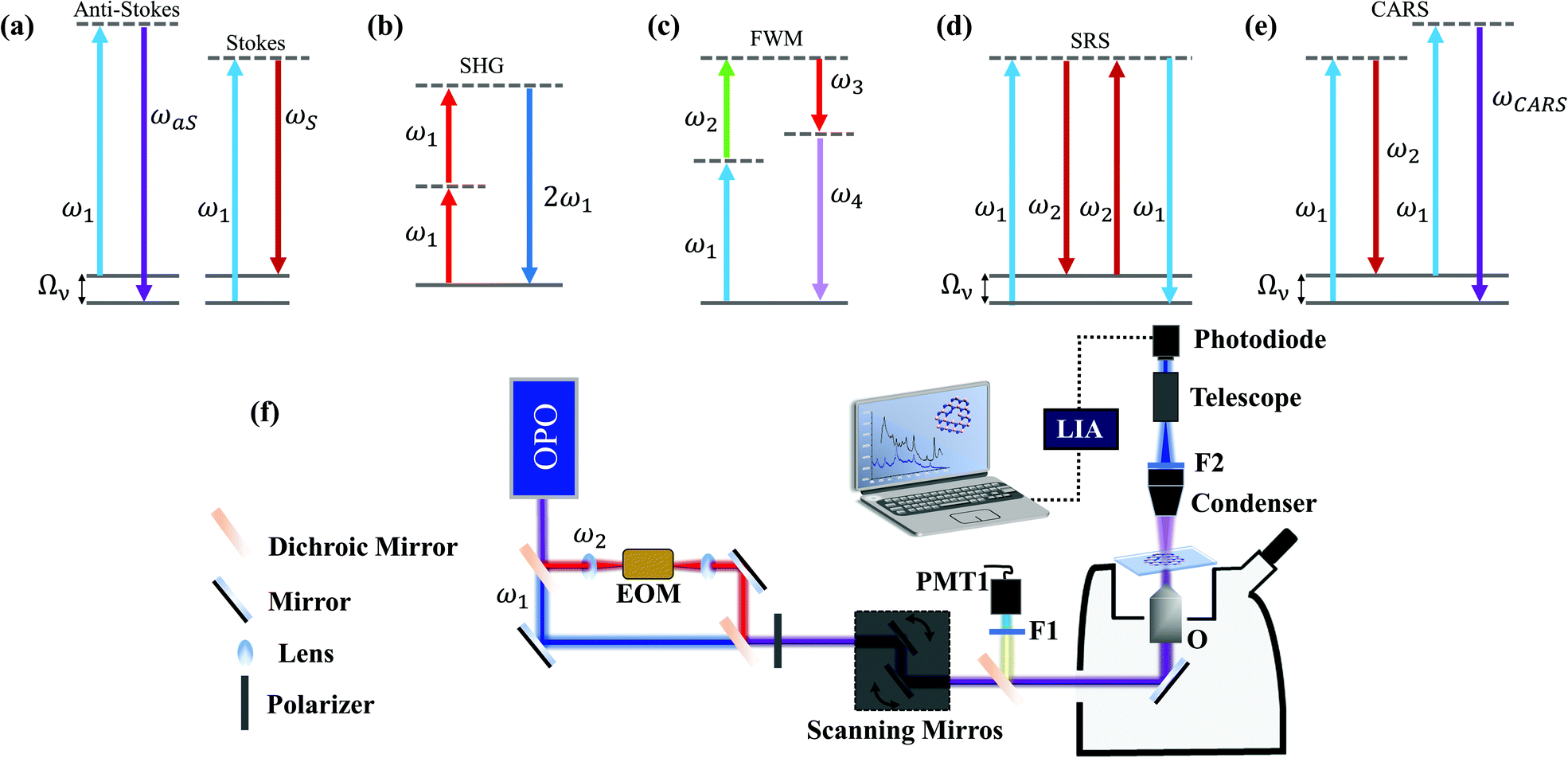 | ||
| Fig. 2 Optical linear and nonlinear effects and experimental implementation. Energy level description for (a) anti-Stokes and Stokes linear (spontaneous) Raman scattering, (b) second harmonic generation, (c) general (phonon-unrelated) four-wave mixing (FWM), (d) stimulated Raman scattering (SRS) and (e) coherent anti-Stokes Raman scattering (CARS). (f) Experimental setup for nonlinear imaging. A tunable pulsed laser source (OPO) can provide different excitation wavelengths for imaging and spectroscopy. For general FWM and CARS, the backscattered signal is detected by a photomultiplier (PMT1) with a suitable band-pass filter (F1). The forward SRS is detected by a large-area photodiode with a filter (F2) blocking the beam initially modulated by the electro-optic modulator (EOM, not needed for CARS). The initially unmodulated beam is detected through a modulation transfer scheme mediated by a lock-in amplifier (LIA). | ||
When the amplitude of the electric field becomes sufficiently large as compared to the intra-atomic fields, the optical phenomena do not match the simple linear description of eqn (1). Under this regime, the polarization P(t) can be written perturbatively as a power series:50
| P(t) =ε0(χ(1)E(t) + χ(2)E2(t) + χ(3)E3(t) + …). | (2) |
The first nonlinear term, driven by χ(2), is a wave mixing effect known as second harmonic generation (SHG).50,54 As shown in Fig. 2(b), this three-wave mixing process is characterized by the conversion of two incoming low-energy photons at ω1 into one photon with exactly twice the incident frequency,50,54 and it is primarily related to the second term of expansion (2). Due to its coherent and symmetry-sensitive nature,50,54 in a scanning laser microscope setup with a short-pulsed source, as in Fig. 2(f), SHG enables rapid imaging, providing rich crystallographic information. Such properties make SHG an important technique for the study of many 2D materials.55–67
Fig. 2(c) shows a four-wave mixing process, but now related to χ(3) in the third-order term in expression (2). Three fields are mixed in a nonlinear medium and produce a fourth field, characterizing the process of traditional four-wave mixing (FWM).50,54 There are several possible energetic configurations for the FWM process in Fig. 2(c), for different choices of ωi, and our focus here is on the nonlinear Raman spectroscopies, namely coherent anti-Stokes Raman spectroscopy (CARS) and stimulated Raman scattering (SRS), which are techniques where the Raman cross-section is enhanced significantly by optically stimulating phonons in the materials in the third-order process in eqn (2).
When two fields at frequencies ω1 and ω2 interact coherently in a nonlinear medium, Raman-mediated effects arise when the beating frequency (ω1 – ω2, with ω1 > ω2) is resonant with a vibrational transition at Ων.41Fig. 2(d) shows the conversion of ω1 into ω2, stimulated by the presence of the beam at ω2 at the cost of leaving the material in an excited vibrational state. Such a process is stimulated Raman scattering (SRS).41,50,54 Simultaneously, the beam at ω2 also stimulates a FWM process that generates the ωCARS frequency at 2ω1 – ω2, which characterizes the coherent anti-Stokes Raman scattering (CARS)41,50,54 in the diagram in Fig. 2(e). In both cases, the stimulated generation of ω2 and ωCARS (in SRS and CARS, respectively) is orders of magnitude more likely to occur than in the spontaneous Raman scattering in Fig. 2(a).41,68 As a Raman-mediated four-wave mixing, SRS and CARS probe vibrational states, therefore providing also chemical fingerprints of the materials. The fundamental difference between CARS and SRS is that the first is a parametric effect, while the second is a dissipative effect. In CARS, the interaction between the fields takes place without changing the final state of the material, i.e. the full process is coherent. Experimentally the CARS signal is measured by a photomultiplier with an appropriate band pass filter at the anti-Stokes Raman frequency, as shown in Fig. 2(f). On the other hand, the SRS occurs only when there is an energy transfer, leaving the material in an excited vibrational state.41 This ensures no interference between SRS and non-resonant FWM processes, which gives the technique a better signal-to-noise ratio. Experimentally, for measuring SRS the laser at the Stokes frequency is intensity-modulated and the pump laser intensity is measured by a photodiode at the same modulation frequency, by using a lock-in amplifier after the sample, as shown in Fig. 2(f). Combined with the stimulated nature of the process, SRS allows Raman-specific and high-speed imaging with excellent contrast, which can be used to study 2D materials.
The applications of CARS and SRS will be discussed in Section 2.1 for graphene, Section 3 for h-BN and Section 4.1 for TMD semiconductors.
1.3 Overcoming the diffraction limit using TERS
The idea of using the near-field to overcome the limitation of spatial resolution imposed by light diffraction in optics was proposed in 1928.69 However, the experimental implementation of this idea in the visible spectral range had to wait for the development of scanning probe techniques,70–72 since in this frequency range the near-field is lost in a few nanometers away from the emitter. Although different technological approaches have been utilized to implement this technique, as described extensively in the literature (see ref. 42 and references therein), here we focus on the most promising solution for addressing 2D systems, which is tip-enhanced Raman spectroscopy (TERS;73–80 we will also address tip-enhanced photoluminescence – TEPL70,81,82).The technical aspects behind a tip-enhanced system are shown in Fig. 3, in which panel (a) illustrates the combination of an optical spectroscopy system with a scanning probe microscope driving the optical tip or nanoantenna. The optical system is composed of devices for excitation and back-scattered detection of the optical spectra, including a laser, a spectrometer and a diversity of optical devices to condition the laser beam, which has to be properly coupled to the nanoantenna.83Fig. 3(b) illustrates the region wherein the far-field emission from the objective is focused at the nanoantenna (tip).84Fig. 3(c) shows a simulation of the local field near the tip apex, thus generating the local (near-field) tip-enhanced field.85 The sample is located a few nanometers below the tip and raster-scanned, thus generating hyperspectral data that can be used to generate 2D images.
 | ||
| Fig. 3 (a) Schematics of a tip-enhanced nano-optics system. The sample is located in the XY positioning stage, where the excitation field, coming for a laser, reaches the sample and the nano-antenna. This exemplary system works in a back-scattering configuration, with the optical system at the bottom and the scanning probe system at the top.83 (b) Schematics of the excitation field focus (reddish), where the nano-antenna (tip, yellowish) has to be positioned,84 near the sample on the transparent substrate (grayish). (c) Field intensity simulation (bright colors indicate high fields) near the tip apex. The arrows indicate the field vectors at the sample surface.85 Reproduced with permission from ref. 83 and 85. | ||
Tip-enhancing strategies are especially challenging when addressing 2D materials80,86 because the illumination of the nano-antenna is performed with a propagating field, which therefore illuminates the sample over a much larger area (micrometric dimensions) as compared to the locally antenna-enhanced field (nanometric in size). This competition is not relevant when addressing zero-dimensional (0D) structures, for instance, a molecule or a single defect in a 2D crystal lattice, or even a one-dimensional emitter, such as a carbon nanotube or the edge of a 2D material. However, to address local changes in the intrinsic properties of 2D systems, the nano-antenna enhancement has to be enough to overcome the signal coming from an area roughly 103–104 times larger. Such enhancements are obtainable in surface-enhanced Raman scattering (SERS) because ultra-high fields are generated in the hot-spots, the gap between plasmonic-resonant nanoparticles (gap-mode configuration). The same is not true, however, for TERS in a non-gap mode configuration. For this reason, substantial efforts have been devoted in the TERS community to develop efficient nano-antennas.82,87–89 The recently developed plasmon-tuned tip pyramid (PTTP) is especially interesting,90–92 which enabled two-orders of magnitude spectral enhancements91,92 and the observation of crystallographic Moiré structures in low-angle twisted bilayer graphene (TBG).93
The science of 2D systems based on TERS (and some TEPL) will be discussed in Section 2.2 for single-layer graphene, Section 2.3 for low-angle twisted-bilayer graphene and Section 4.2 for layered semiconductors in the family of transition metal (di)(mono)chalcogenides.
2 Graphene
2.1 CARS
Four-wave mixing studies in graphene were done by Hendry et al. in 2010, where the authors obtained a large value of the third-order electrical susceptibility of graphene.97 Other authors have characterized the χ(3) of graphene by different techniques, such as third-harmonic generation, and also reported large susceptibility values, opening up different possible applications.67 However, none of these studies utilized laser energies that are close to resonance with phonon energies, which is the condition for CARS (see Section 1.2). When the FWM is in the CARS condition, it is expected that the anti-Stokes signal will be enhanced due to the resonance with the phonons, i.e. ω1 – ω2 = Ων. Unexpectedly, Lafeta et al. showed that, in the case of graphene, the FWM signal intensity decreases when in resonance with the phonon energy.94 This phenomenon occurs in graphene because it is a zero-gap semiconductor with a strong contribution of electronic transitions to the third-order nonlinear electrical susceptibility,94 and not only due to transitions involving the phonon state, as depicted in Fig. 4(a). In order to understand this effect in more detail, it is convenient to separate the third-order polarization in two parts: a nonvibrationally resonant background (NVRB) polarization (P(3)NVRB) and a vibrationally resonant background (which we call CARS, for convenience) polarization (P(3)CARS).95,98 Because the intensity measured at the anti-Stokes frequency is given by I(ωas) ∝ |P(3)CARS + P(3)NVRB|2, there is an interference between the two terms that can lead to a decreased intensity at the anti-Stokes frequency, when ω1 – ω2 = Ων.94,95Fig. 4(b) shows the FWM spectrum of graphene taken at different values of pump laser energy (ω1), where it is possible to observe that the intensity decreases exactly at the G-band phonon energy, as confirmed by linear Raman spectroscopy (see the bottom graph of Fig. 4(b)).94 | ||
| Fig. 4 (a) Band structure of graphene (cones) and the CARS process (arrows) where two laser frequencies ω1 and ω2 interact with the material generating an anti-Stokes signal at ω4 = ωCARS frequency. (b) Top: CARS (ω4) intensity as a function of the ω1 pump wavelength (bottom scale) or ħω2 – ħω1 in wavenumbers (top scale) for graphene on a quartz substrate. The bottom graph shows the Raman spectrum taken in the same energy range.94 (c) CARS spectra of few-layer graphene at different delay times between the ω1 and ω2 laser pulses. (d) I: CARS images of two few-layer graphene flakes; from top to bottom: outside vibrational resonance, under vibrational resonance, and by posterior calculations. II: intensity line profiles along the sample (dashed lines in I) and substrate (full lines in I).95 (e) The graph on the left side shows the SWCNT (1) and graphene (2) CARS spectra. The leftmost image shows a CARS image of the SWCNT/graphene system obtained at 1585 cm−1 at resonance with the phonon. The next image is the same sample region but taken at 1610 cm−1, outside the phonon resonance. The rightmost image is the difference between the previous images obtained at 1585 cm−1 and 1610 cm−1. Points no. 1 and no. 2 represent the SWCNT and graphene locations, respectively.96 Reproduced with permission from ref. 94–96. | ||
Moreover, Virga et al. showed that the temporal evolutions of P(3)NVRB and P(3)CARS are significantly different, where in the case of NVRB the FWM interactions must take place within the dephasing time of the involved electronic transitions, which is close to 10 fs for graphene.95 On the other hand, the phonon dephasing time in graphene is much longer (1 ps), and hence while P(3)NVRB has a fast dephasing time, P(3)CARS has a much longer dephasing time. This effect is shown in Fig. 4(c) where the anti-Stokes intensity is measured for different delay times between the two laser pulses. At zero delay time, the CARS spectra shows a decreased intensity at the phonon energy. However, when the delay time is increased, the CARS intensity slowly increases and reaches a maximum at longer delay times, corresponding to the P(3)CARS term.95
For performing CARS imaging in graphene, one needs to take into account the strong contribution of the FWM signal from electronic transitions. Virga et al.95 accomplished this by measuring a set of images as shown in Fig. 4(d) in panel I. In the first image (from top to bottom) the authors have measured the CARS intensity of few-layer graphene at a frequency away from the phonon resonance, with a strong contribution from P(3)NVRB. In the second image, they have displayed the CARS intensity at the phonon resonance where both P(3)NVRB and P(3)CARS have contributions. In the third image, the authors have performed a calculation based on the first two images to obtain a high contrast CARS image.95Fig. 4(d) in panel II shows an intensity profile along the graphene flake (top graph with dashed lines) and at the substrate (bottom graph with full lines). It is possible to observe that the procedure for producing the CARS image shown in panel I have a small intensity coming from the substrate and a high intensity coming from the graphene flake, therefore enabling high contrast CARS imaging in graphene.95
Fig. 4(e) shows another example of CARS imaging in graphene together with single-walled carbon nanotubes (SWCNT)99 using a similar methodology.96 The first graph (on the left) shows the CARS spectra of both graphene and SWCNT near the G band frequency, where it is possible to observe the decreased intensity of CARS near the phonon energy for graphene (spectrum 2), but an enhanced intensity for SWCNT (spectrum 1). In the first CARS image taken in resonance with the phonon energy, both SWCNT and graphene are located in the highlighted regions 1 and 2, respectively. On the other hand, away from the phonon resonance (second CARS image) the SWCNT signal disappears, while the graphene signal remains due to the signal coming from the non-resonant contributions, as discussed before. Finally, in the last CARS image the authors performed a subtraction between the first two images, showing that the signal coming from the SWCNT is enhanced in the image compared to the signal coming from graphene.96
2.2 TERS in graphene
One-dimensional (1D) carbon nanotubes were initially explored as an important prototype for the development of tip-enhanced Raman spectroscopy (TERS),75,102–105 mostly due to their strong resonant Raman scattering associated with their 1D structure. Later on, 2D graphene became a protagonist of the development of fundamentals and applications of TERS, for reasons we explore here.TERS has been utilized to identify local strain and doping in in-plane homojunctions in graphene devices, built as van der Waals heterostructures where the graphene is half sitting on talc and half on SiO2.106 The high spatial resolution of TERS enables the observation of the charge depletion region at the interface between different substrates. Furthermore, local strain and doping can also result simply due to the presence of particles in the substrate107 or due to non-homogeneous deposition when forming twisted bilayer graphene.108 Such non-homogeneity is only identifiable with nano-Raman, while it is averaged out in usual micro-Raman analysis.108
More than just improving imaging spatial resolution, the different symmetries and dimensionalities of the features composing the Raman spectrum of graphene provide a fertile source of new phenomena occurring in the near-field regime and reveal the important aspects of TERS.109,110 The most fundamental one is the influence of interference effects on the TERS signal.100,111 Spatial correlations of phonon modes can be neglected in conventional Raman spectroscopy experiments performed in the far-field regime because the correlation length Lc of optical phonons in crystals is one order of magnitude shorter than the wavelength of visible light.111,112 According to the early theory of coherence, optical fields present correlation lengths of at least half of their associated wavelength in the far-field regime.113 Therefore, the information on shorter correlations of the source is lost when the signal transits to the far zone (more than half wavelength far from the source). For this reason, Raman scattering is usually treated as a spatially incoherent process in classical textbooks,114 which do not account for the near-field components of the scattered field. However, with the advent of TERS, it has been shown that this approach is not valid when the non-radiating near-field components are taken into account.86,100,110,111,115 Due to coherence, the Raman intensity at the nanoscale depends on the symmetry and spatial confinement of the vibrational mode. The characteristic length that defines this spatial correlation can be extracted from the different levels of enhancement measured for distinct modes. In short, the interference is destructive for the G band signal, associated with phonons with E2g symmetry, and constructive for the D and 2D bands, associated mostly with totally symmetric A1g phonons110 (see Fig. 5(a)). As such, the interference effects give rise to a weaker tip–sample distance dependence for the G band than for the D and 2D bands, making it possible to extract the correlation length Lc ∼ 30 nm from the measured data.100,111 Moreover, if the D band signal originates from edges (1D structure), a further change of the tip–sample distance dependence is observed. The experimental evidence for these coherence phenomena was first reported in ref. 111. Later on, similar effects were reported for GaS116 (see Section 4.2).
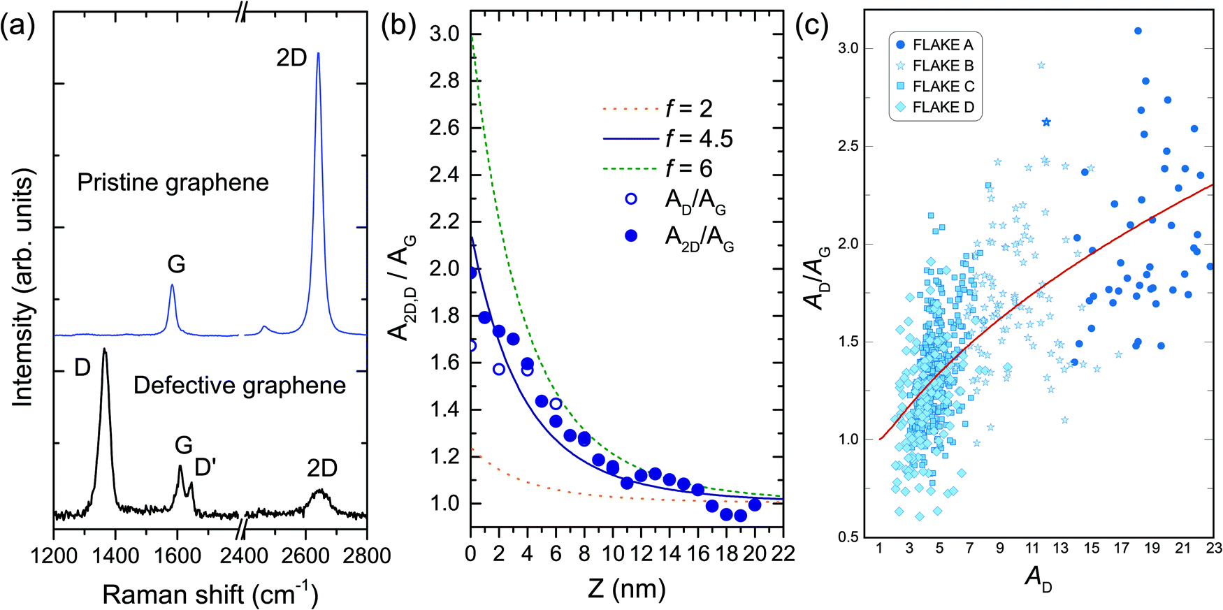 | ||
| Fig. 5 (a) At the top, the Raman spectrum of pristine graphene composed of the one-phonon first-order allowed G band (≈1580 cm−1) and the two-phonon 2D band (also called G′ in the literature) centered at ≈2700 cm−1. In the presence of structural defects that break the translational symmetry of the graphene lattice, the Raman spectrum is also composed of the disorder-induced D and D' bands, centered at ≈1350 and 1620 cm−1, respectively, as shown in the bottom spectrum. (b) Solid circles: experimental data extracted from the ratio of the integrated areas of the 2D and G bands (A2D and AG, respectively), measured from a pristine graphene sample as the near-field probe (a plasmon-tunable tip pyramid – PTTP)90–92 approaches the surface by shortening the tip–sample distance Z. Open circles: AD/AG data from the tip-approach procedure conducted in a defective graphene nanoflake. Solid blue line: fitting of A2D/AG as a function of Z according to the theory developed in ref. 100. The fit indicates a field-enhancement factor f of approximately 4.5. Orange dotted and green dashed curves: plots of theoretical calculations considering hypothetical experiments with PTTPs that provide field-enhancement factors of 2 and 6, respectively. (c) Scatter plot of AD/AG values as a function of AD for four distinct nanoflakes (marked by distinct symbols) investigated in ref. 101. The red solid line is the result of a theoretical fit of the data points using a relation developed in ref. 101 based on the theoretical background introduced in ref. 100. From left to right, the red line defines a trajectory for larger values of the enhancement factor f giving rise to larger values of AD/AG. The values of AD, AG and A2D in (b) and (c) are normalized to their respective far-field values. Reproduced with permission from ref. 101. | ||
Besides the correlation length of optical phonons, the distinct behavior of the 2D and G bands in the near-field regime can be used as a measurement for the enhancement achieved in a TERS experiment. This effect is summarized in Fig. 5(b), reproduced from ref. 101. The solid circles are the experimental data extracted from the ratio of the integrated areas of the 2D and G bands (A2D and AG, respectively), measured from a pristine graphene sample as the near-field probe (a plasmon-tunable tip pyramid – PTTP)90–92 approaches the surface by shortening the tip–sample distance Z. The values are normalized to the far-field signal so that A2D,D/AG → 1 for larger values of Z. As shown in the graphics, for the minimal distance at Z → 0 (which means the tip is roughly 5 nm away from the sample), the enhancement of the 2D band is approximately twice the enhancement exhibited by the G band, with the difference decreasing as Z increases. The blue solid line is a fitting of A2D/AG as a function of Z according to the theory developed in ref. 100. The fit indicates a field-enhancement factor f of approximately 4.5. This enhancement factor is related to the tip polarizability, and it is a measure of its strength for local field enhancement. The orange dotted and green dashed curves are plots of theoretical calculations considering hypothetical experiments with tips that would provide field-enhancement factors of 2 and 6, respectively.
In the presence of structural defects that break the translational symmetry of the graphene lattice, the Raman spectrum is also composed of the disorder-induced D band (≈1350 cm−1), originating from the same TO phonon branch that gives rise to the 2D band, and also by the D′ band (≈1620 cm−1), originating from the LO phonon branch in the proximity of the Γ point [see the bottom spectrum in Fig. 5(a)].4 Because D and D′ require structural defects to satisfy momentum conservation in the double-resonance Raman process, their sources are localized in the defective region, and therefore they have the same dimensionality as the defect itself.117,118 In other words, point and edge defects give rise to D or D′ bands originating from zero- and one-dimensional regions, respectively.25
The graphics also exhibit the AD/AG data (open circles) from the tip-approach procedure conducted in a defective graphene nanoflake. As explained above, since the D and 2D bands have the same symmetry, they are indeed expected to exhibit the same near-field interference properties. Therefore, the dependence of the AD/AG ratio on the field enhancement factor has important metrological consequences in terms of determination of defect density in graphene by TERS.101 It is well known that the AD/AG ratio is sensitive to the amount of structural defects.9,25,29,112,117 In the absence of sp3 bonds, the AD/AG ratio is inversely proportional to the squared average distance between point defects LD2,25,117,119 or to the average crystallite size, La, in the case of linear defects.25,112,120 For conventional Raman spectroscopy, these relations were established through the measurement of prototype samples with LD and La previously determined by scanning tunneling microscopy (STM).112,117,120 However, because the enhancement factor influences the value of the AD/AG ratio, as demonstrated in ref. 101 and 111 (see Fig. 5(c) and related text), metrological protocols that take into account the enhancement factor of the near-field probe used in the experiment have to be developed101 for quantitative analysis with TERS. This is an open field for TERS application.
2.3 TERS on twisted bilayer graphene
The ability to precisely tune the angle between two layers of graphene opens the possibility for an extra degree of nanomanipulation that led to the discovery of unconventional superconductivity in twisted bilayer graphene (TBG) at the so-called magic angle (twist angle θ ∼ 1.1°).121,122In real space, twisted homo-bilayer heterostructures form an artificial lattice, frequently called moiré patterns, whose lattice constant (Lm) is angle-dependent following the equation:  where a0 is the single-layer lattice constant. Lm ≥ 10 nm for angles θ ≤ 1° in twisted bilayers from graphene, hexagonal boron nitride (h-BN) and TMDs. Recently, Yoo et al. showed that, for θ ≤ 1°, the TBG experiences an energetically favorable atomic reconstruction, generating the so-called reconstructed twisted bilayer graphene (rTBG),123 where the carbon atoms rearrange to maximize the AB and BA stacking regions, alternating black and gray triangles, as shown in Fig. 6(a). The AB and BA stacking are similar but differ by a reflection operation. Moreover, saddle point (SP) solitons (frequently called just solitons) separate the AB/BA domains. Finally, the interception between the SP solitons forms topological AA stacked points (Fig. 6(a)). Notably, TMDs also show reconstruction below a critical angle.124 Here, we focus on near-field imaging of rTBG because of its particular arrangement with well-defined regions.
 | ||
| Fig. 6 (a) Representation of rTBG. (b) Sketch of rTBG imaging by nano-Raman highlighting the TERS tip (PTTP – plasmon-tuned-tip pyramid). (c) Nano-Raman rTBG map recorded from the G′ (also named 2D) band intensity. (d) G-band FWHM nano-Raman map acquired at the dashed square in (c). (e) Nano-Raman G-band spectra recorded in AA (red), SP (blue) and AB/BA regions. The left panel data were acquired in the same sample as in (d), and the right panel data were from another location with a single soliton. (f) Nano-Raman G′ spectra from the AB/BA (left) and SP/AA (right) regions. Reproduced with permission from ref. 93. | ||
So far, most near-field studies in rTBG used infrared (IR) excitation (with excitation energies ranging from 100 to 200 meV).125–127 Nano-IR successfully investigated plasmonic, electronic and thermoelectric rTBG solitonic properties, but this technique has two significant limitations that prevent a complete investigation over rTBG quantum properties: (1) most of the in-plane rTBG phonons are IR dipole-forbidden;128 (2) the tips for nano-IR generate a relatively low near-field signal.125–127 In contrast, TERS-based nano-Raman spectroscopy gives a multi-assessing tool, allowing phonon, electron, electron–phonon coupling and stacking-order investigations in rTBG. The TERS nanoantenna (see Fig. 6(b)) induces localized near-field signals orders of magnitude larger than the far-field signals, providing a pure near-field contribution restricted to the tip apex location. Fig. 6(c) presents a nano-Raman map recorded from the rTBG G′ (also named 2D) band intensity.93 The map unravels an Lm = 160 nm (θ = 0.09°) rTBG crystallographic structure, where the AB/BA, SP, and AA stacking regions are observed. Note that nano-Raman does not distinguish AB/BA because their Raman selection rules are the same.
Besides revealing the crystallographic structure of rTBG using visible light, nano-Raman carries rich physical information. Close to the Fermi level, the low-energy G phonons (Eph ≈ 197 meV) mediate electronic transitions, enhancing the electron–phonon coupling (EPC). As the EPC increases, the G phonon lifetime decreases and enlarges the full-width at half maximum (FWHM),26,28i.e. the G band FWHM indirectly probes the EPC. Fig. 6(d) presents the image of the G band FWHM over the dashed square in Fig. 6(c). The FWHM outlines the rTBG crystallography where higher values of FWHM (i.e. higher EPC) are observed at the AA sites due probably to density of states localization.129,130 Nevertheless, Xie et al. also showed that a strong electron–electron interaction is expected at the AA points131 and similarly for the EPC in Fig. 6(d). So Fig. 6(d) indicates the possibility that the EPC plays a role in TBG superconductivity.
Fig. 6(e) presents the nano-Raman G spectra acquired in the AA (red), SP (blue), and AB/BA (black) regions. The data from the left panel were acquired from the sample in Fig. 6(d), while the right panel displays data from another location near a single soliton. All the spectra exhibit a pronounced G band, but at the SP and AA locations they also present higher and lower frequency peaks, named Gr+ and Gr−, respectively. Gadelha et al. revealed that the Gr+ mode is mostly observed at the SP, while the Gr− at the AA.93 A state-of-the-art nearly free phonon model also supports the results.129
On the other hand, the electronic structure, stacking order, and other factors impact the G′ mode. Fig. 6(f) presents the nano-Raman G′ spectra acquired in the AB/BA (left panel) and SP/AA (right panel) regions. The AB/BA nano-spectrum is identical to that of Bernal-stacked bilayer graphene, composed of four peaks (see Fig. 6(f)), as expected.15 However, the SP/AA spectrum exhibits an unusual lineshape, providing a unique Raman signature. Therefore, Fig. 6(e and f) manifest a localization of both the phononic and electronic rTBG aspects.129,130
3 Hexagonal boron nitride – CARS and SRS
Similar to the case of graphene (see 2.1), Lafeta et al. studied the FWM response of h-BN close to the CARS condition. The band structure of h-BN is schematically shown in Fig. 7(a), where it is indicated that h-BN is an insulator with a high value of band gap. Therefore, the CARS process in h-BN does not have a contribution from the electronic NVRB, and the CARS spectra will have only contributions from the phonon resonance. The CARS spectra of h-BN are shown in Fig. 7(b), where it is possible to observe an enhancement when both lasers have an energy difference matching the phonon energy, which is corroborated by the Raman spectra shown in the bottom graph.94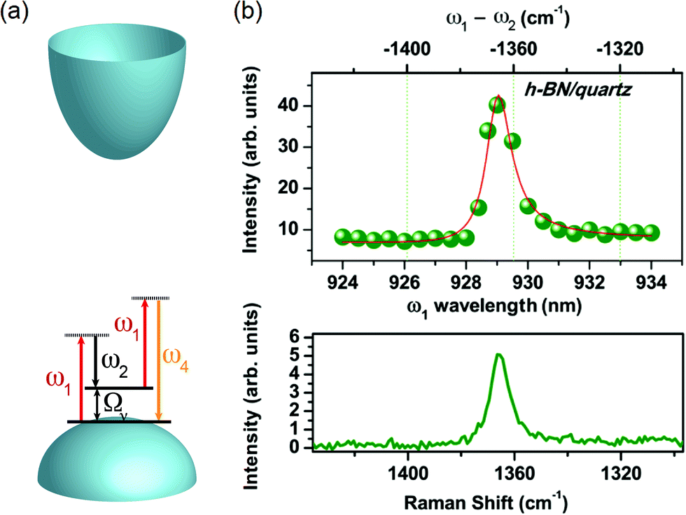 | ||
| Fig. 7 (a) Schematics of the band structure of h-BN (paraboloids), which is an insulator, with the diagram of the CARS process (arrows), where two lasers of frequencies ω1 and ω2 interact with the material generating an anti-Stokes signal at the ω4 frequency. (b) CARS spectra of few-layer h-BN as a function of the ω1 wavelength (bottom scale) and ħω2 – ħω1 in wavenumbers (top scale) for few-layer h-BN. The Raman spectrum of the same sample is shown in the graph below. Reproduced with permission from ref. 94. | ||
As discussed in Section 1.2, the stimulated and dissipative nature of SRS allows the study of materials by rapid imaging and spectroscopy. In the case of h-BN, this is of particular importance. As a wide bandgap material, it can be difficult to study its properties using absorption-based optical contrast techniques. In addition, its E2g Raman-active mode is far from electronic resonances, giving h-BN a weak Raman signal when compared to other 2D materials. The E2g mode is about 50 times stronger in graphene.132 While this limits the research of h-BN through spontaneous Raman scattering, this also illustrates one of the main advantages of SRS. Fig. 8(a)and (b) show high-resolution images of a mechanically exfoliated h-BN flake and a large area image with several flakes, respectively, both obtained by SRS with a total acquisition time of less than one minute.
 | ||
| Fig. 8 (a) SRS image of an h-BN flake and (b) a large-area image of a different area of the sample obtained with a high numerical aperture objective in a setup similar to the one in Fig. 2(e). (c) AFM and (d) SRS images of an h-BN sample. (e) AFM heights and SRS intensities along the lines shown in (c and d). (f) Dependence of SRS intensity on flake thickness. Reproduced with permission from ref. 136. | ||
Although SRS is widely used in bioimaging,41,133–135 it has only recently been applied to study 2D materials and, in particular, h-BN.136 While spontaneous Raman scattering has been used to characterize the number of layers of few-layer h-BN, some authors44,136 call attention to discrepancies between some results and extensions for multilayers.132,137–140 Using SRS, Ling et al.136 addressed this controversy, measuring 35 mechanically exfoliated flakes with thickness ranging from 2.5 nm to 70 nm. Fig. 8(c) and (d) show, respectively, the AFM and SRS images of an h-BN flake. We can immediately observe a close correspondence, suggesting a relation between the thickness of the material and the SRS intensity. A line profile across the regions of different thicknesses (see locations in Fig. 8(c) and (d)) allows the comparison of the intensity profiles from AFM and SRS, which shows the very well-matched curves in Fig. 8(e). From the intensity profiles of AFM and SRS, Ling et al. obtained the linear dependence of SRS intensity on sample thickness, as shown in Fig. 8(f). This result suggests the possibility of using SRS to quantify sample thickness in a rapid manner. It is worth mentioning that, regarding Raman spectroscopy in non-transparent media, the penetration depth depends on the laser wavelength and the material index of refraction, ranging from a few nanometers to hundreds of microns. In the case of h-BN, which is transparent at the laser energies typically used for SRS, the material thickness can be probed. Moreover, the authors acquired the SRS images with a pixel dwell time that is 4 orders of magnitude smaller compared to conventional spontaneous Raman microscopy, highlighting the promising use of the technique in the research of h-BN.
4 2D semiconductors
4.1 CARS
CARS has not yet been widely applied to the study and imaging of 2D semiconductors, such as TMDs, mainly because of their low vibrational frequencies as compared to other 2D materials, such as graphene and h-BN. In commonly available laser systems, there are experimental difficulties in matching the pump and Stokes laser energies with the low vibrational frequencies in these materials. Nevertheless, multiplex CARS spectroscopy was used by Ko et al. to investigate processes in bulk MoS2.141 The authors have used a photonic supercontinuum fiber to generate a broad band Stokes pulse ranging from 800 to 1100 nm and a narrow band pump pulse centered at 800 nm. The measured CARS spectra were characterized by a broad peak corresponding to the four-wave mixing signal of MoS2 and another peak centered at approximately 680 nm, corresponding to a resonance with the A exciton. Moreover, the authors identified a smaller peak in the CARS spectra that corresponds to a vibrational energy of 634 cm−1, which corresponds to a combination between A1g and LA(M) phonons.141 Further progress needs to be made in order to overcome the experimental limitations for performing CARS in TMDs and other 2D materials with low frequency Raman modes.4.2 TERS
After graphene, the TMD MoS2 (see Fig. 1(g)) is the most studied 2D material using TERS. The first report of tip-enhanced measurements in MoS2 shows a nanoscale mapping of excitons and trions by combining TERS and TEPL, with a spatial resolution of less than 20 nm.146 The authors also investigated doping by using Ag and Au coated tips and found that the type of doping depends on the work function of the metal, n-doping for Ag and p-doping for Au. Thus, using an Ag coated tip, it was possible to create a TEPL mapping of the A0 exciton and for the A− and B− trions in single-layer MoS2. Following this work, other authors contributed to the development of this field. For instance, a giant gap-mode TERS was performed in MoS2 with the aid of a nanocluster array on the substrate.142 As shown in Fig. 9(a), a 108 enhancement was observed for the A1g peak. Notice the A1g was enhanced much more than the E2g, consistent with the near-field coherence effect discussed for graphene (Section 2.2).100,111 This large enhancement is attributed to the presence of nanodisks of gold on the substrate (displayed on the right side of Fig. 9(a)), creating the gap-mode regime that provides high enhancement on the edges of the disks. The authors also observed a plasmonic hot electron doping of monolayer MoS2 due to the presence of the tip and the nanodisks on the substrate, which caused a transient structural phase transition from 2H to 1T.19 | ||
| Fig. 9 (a) Giant gap-plasmon TERS on the TMD MoS2 spectrum (left) on top of a substrate with gold nanodisks (right). The strong signals are recorded at the edges of the nanodisks.142 (b) Tip-approach measurement that implies the spatial phonon length of the TMM GaS.143 (c) Comparison of non-resonant (top) and resonant (bottom) TERS of TMD MoSe2 and TERS image of the flake.144 (d) TERS and TEPL spectra of the TMD WSe2 as a function of the tip–sample distance.145 Reproduced with permission from ref. 142–145. | ||
TERS has also been used to study highly localized strain in MoS2/Au heterostructures induced during the formation of such a heterostructure, in which the maximum shift reported for the E2g mode was (4.2 ± 0.8) cm−1, corresponding to a 1.4% biaxial strain.147 TERS has been used to study nanoscale defects and wrinkles on MoS2 with a spatial resolution of ∼18 nm, identifying localized inhomogeneities148 and probing edge-related properties in few-layer MoS2.149
More recently, the local doping variations in the depletion region in in-plane homojunctions in MoS2 devices have been imaged using tip-enhanced photoluminescence (TEPL).106 In TEPL, the local luminescence is measured rather than the phonon scattering, and Gadelha et al. used the spatial oscillation of the exciton and trion frequencies to image doping variations with nanometer resolution.
Other 2D materials have also been investigated by TERS, such as TMM gallium sulfide (GaS),143 which is interesting for having two different Raman active A1g modes. The authors reported that the phonon coherence length (Lc) for five-layer GaS is different for the A11g phonon (Lc ∼ 64 nm) and for the A21g phonon (Lc ∼ 47 nm). The Lc values were determined through the tip-approach experiment, which consists of moving the tip out from the sample at fixed steps and recording the Raman spectrum at each point, as displayed in Fig. 9(b) for the A11g peak. In order to do so, a curve must be fit to the experimental data that have Lc as one of its parameters, similarly to what was done in graphene.111 As Lc becomes larger, so does the TERS enhancement. Additionally, they showed that Lc decreases as the number of layers decreases, suggesting that scattering with the surface of the substrate has a major role in the phonon decay process.
Back to TMDs, in monolayer MoSe2, TERS has also been used to reveal nanoscale heterogeneities, by combining it with different scanning probe microscopy techniques.144Fig. 9(c) shows a non-resonant and a resonant TERS spectrum (top and bottom of Fig. 9(c), respectively). In the former, only one dominant peak at around 240 cm−1 (blue) is clearly distinguished, while in the latter there are other Raman peaks at 287 cm−1 (red) and 340 cm−1 (green). When comparing these measurements with α-MoO3 TERS, it was possible to infer that these differences from non-resonant and resonant TERS spectra were due to the inclusion of MoO3 in the MoSe2 matrix.
In tungsten diselenide (WSe2), TERS and TEPL nanospectroscopy and nanoimaging were combined, as shown in Fig. 9(d). Fig. 9(d) shows the Raman and PL spectra acquired at different tip–sample distances, showing the E2g (E′) and A1g respectively, at around 273 cm−1 and the first (150 cm−1) and third (405 cm−1) order LA phonons.145 The authors also suggest that the shoulder in the TEPL spectra might have originated from the rise of trion or biexciton emissions. These features allowed the study of monolayer WSe2 grown by physical vapor deposition of the associated nanoscale heterogeneities in the form of edges, grain boundaries and nucleation sites, extracting information about correlations of the photoluminescence spectral intensity, shifts with crystal edges and exciton diffusion length. The data suggest an approximately 25 nm exciton diffusion length, inferred to be due to the spatial scale of the photoluminescence quenching, and an around 30 to 80 nm wide region of optical heterogeneity at the edges. Still on WSe2, it was also reported that other metals, besides Au and Ag, can be used to prepare a substrate for gap-mode TERS,150 showing similar TERS measurement results for WSe2 on Au and Cr substrates, implying that these results can be extended to other metals.
5 Summary and perspectives
In this article, we have reviewed recent results where different 2D materials were studied by CARS, SRS and TERS. These advanced techniques can overcome the two limitations of standard Raman spectroscopy, i.e. weak signal and low spatial resolution, providing a platform for advancing 2D materials’ related science and also for the development of the techniques, having 2D materials as prototypes. The 2D systems are perfect surfaces and, therefore, a rich platform for experimental and theoretical developments, not only concerning the 2D science, but also on the extremely important interaction of the material with the environment.With the improved signal intensity provided by CARS and SRS, it has been shown that they provide fast Raman imaging, including in large electronic band gap materials (e.g. h-BN), which exhibit very low Raman signals due to the absence of resonant light–matter interactions. Technical improvements are still needed to measure 2D materials with more heavy atoms, due to their low frequency vibrational modes, hardly accessible in the stimulated regime utilized in CARS and SRS. For example, recent developments for performing SRS and CARS at low and THz frequency ranges151,152 have been shown, and therefore they could be applied for imaging other 2D materials like TMDs, TMMs, black phosphorous and others. Moreover the ability to perform THz stimulated Raman imaging opens the opportunity to study not only phonons, but also other quasi-particles such as magnons in magnetic 2D materials.153 Also, the applications of these techniques in heterostructures, including twisted homo- and hetero-bilayers, might also provide rich information. For example, it has been shown that low-frequency Raman modes arise in TMD heterostructures depending on the staking angle,154,155 and therefore SRS and CARS can provide a fast imaging technique to probe the quality and staking order of these heterostructures.
Nano-Raman spectroscopy, as implemented here, based on the TERS effect, is mostly a surface technique and, in this sense, 2D materials represent a prototype for the study of the technique itself. Research about coherence in the near-field regime is in its early stage, with a clear impact of the use of nano-Raman to characterize materials, including the number of defects and local doping and strain of graphene deposited in different substrates. Besides the local study of doping, strain and defects, intentionally or unintentionally introduced in 2D samples and devices, the relevance of interaction with the environment, including contamination in the surface, e.g. a commonly found surface water layer, among others, is a subject to be explored. The tip-approach procedure has been shown to be a unique technique to get information about symmetry and nano-meter sized coherence length for phonon mediated scattering. However, related studies are still limited to two cases (graphene and GaS) and more experimental and theoretical work is needed to fully understand the related effects and how it applies to other 2D materials. The nano-Raman spatial resolution and antenna enhancement properties are still under debate, and here, again, 2D materials might also represent a valuable reference system.156 With these aspects clearly established, nano-Raman can become an odd technique for nanometrology, not only for 2D-systems,157 but back to more complex nano-materials where rich Raman behavior has been observed.158 Besides, most 2D materials from different classes, such as h-BN, phosphorene and many others, are still untouched by the technique.
One potentially important application of nano-Raman is in the twistronics field, where novel phenomena are observed due to potentials fluctuating in the nano-scale. The twist between two 2D layers has been shown to generate interesting results in homo-bilayers, using two identical layers of different 2D materials,124,159 and also in hetero-bilayers,160 where two different layered materials are stacked together. Notably, a new field emerged, named twistronics, where TBG has been shown to exhibit ferromagnetism64 in a quantum Chern insulator,161 large linear-in-temperature resistivity,162 nematicity,163 plasmonic collective excitation164 and tunable photonic crystals125 and, more recently, the localization of lattice phenomena, such as electrons and phonons,93 and the photothermoelectric effect.126 Moreover, interesting effects were observed or predicted in twisted heterostructures of TMDs, such as correlated electronic phases in twisted homo-bilayers of WSe2,165 the prediction of localized excitons in twisted homo-bilayers of MoS2,166 and evidence for moiré excitons in hetero-bilayers of MoSe2/WSe2.160 However, to access moiré pattern related physics, spatial resolution might be a problem. The increased optical resolution in TERS experiments allows the collection of information about defects and phonon coherence length and imaging of moiré patters that is not possible using far-field Raman spectroscopy.
Finally, the combination of TERS with CARS or SRS has the potential to generate high-resolution, information-rich and fast Raman spectral imaging. Given the relevance of Raman spectroscopy as a tool for materials characterization, we believe that this is an important subject for future studies in nanometrology.
Conflicts of interest
The authors declare no conflicts of interest.Acknowledgements
The authors acknowledge Rafael S. Alencar for providing the Raman spectra of GaS and Frederico Souza for the Raman spectra of MoSe2 and WSe2 (shown in Fig. 1). This work was supported by CNPq (302775/2018-8, 429771/2018-5, 306348/2019-5), Finep (442521/2019-7), CAPES (RELAII and 367 88881.198744/2018-01) and FAPEMIG (TEC – RED-00282-16, APQ-02026-17).Notes and references
- L. Malard, M. Pimenta, G. Dresselhaus and M. Dresselhaus, Phys. Rep., 2009, 473, 51–87 CrossRef CAS.
- M. S. Dresselhaus, A. Jorio, M. Hofmann, G. Dresselhaus and R. Saito, Nano Lett., 2010, 10, 751–758 CrossRef CAS PubMed.
- R. Saito, M. Hofmann, G. Dresselhaus, A. Jorio and M. Dresselhaus, Adv. Phys., 2011, 60, 413–550 CrossRef CAS.
- A. Jorio, M. S. Dresselhaus, R. Saito and G. Dresselhaus, Raman spectroscopy in graphene related systems, John Wiley & Sons, 2011 Search PubMed.
- M. A. Pimenta, G. Dresselhaus, M. S. Dresselhaus, L. G. Cançado, A. Jorio and R. Saito, Phys. Chem. Chem. Phys., 2007, 9, 1276–1290 RSC.
- J. N. Coleman, M. Lotya, A. ONeill, S. D. Bergin, P. J. King, U. Khan, K. Young, A. Gaucher, S. De and R. J. Smith, et al. , Science, 2011, 331, 568–571 CrossRef CAS PubMed.
- A. C. Ferrari and D. M. Basko, Nat. Nanotechnol., 2013, 8, 235–246 CrossRef CAS PubMed.
- S. Z. Butler, S. M. Hollen, L. Cao, Y. Cui, J. A. Gupta, H. R. Gutiérrez, T. F. Heinz, S. S. Hong, J. Huang and A. F. Ismach, et al. , ACS Nano, 2013, 7, 2898–2926 CrossRef CAS PubMed.
- M. A. Pimenta, E. del Corro, B. R. Carvalho, C. Fantini and L. M. Malard, Acc. Chem. Res., 2015, 48, 41–47 CrossRef CAS PubMed.
- G. R. Bhimanapati, Z. Lin, V. Meunier, Y. Jung, J. Cha, S. Das, D. Xiao, Y. Son, M. S. Strano and V. R. Cooper, et al. , ACS Nano, 2015, 9, 11509–11539 CrossRef CAS PubMed.
- R. Saito, Y. Tatsumi, S. Huang, X. Ling and M. S. Dresselhaus, J. Phys.: Condens. Matter, 2016, 28, 353002 CrossRef CAS PubMed.
- P.-H. Tan, Raman Spectroscopy of two-dimensional materials, Springer, 2018, vol. 276 Search PubMed.
- X. Cong, X.-L. Liu, M.-L. Lin and P.-H. Tan, npj 2D Mater. Appl., 2020, 4, 1–12 CrossRef.
- H. B. Ribeiro, M. A. Pimenta and C. J. de Matos, J. Raman Spectrosc., 2018, 49, 76–90 CrossRef CAS.
- A. C. Ferrari, J. C. Meyer, V. Scardaci, C. Casiraghi, M. Lazzeri, F. Mauri, S. Piscanec, D. Jiang, K. S. Novoselov and S. Roth, et al. , Phys. Rev. Lett., 2006, 97, 187401 CrossRef CAS PubMed.
- H. Li, Q. Zhang, C. C. R. Yap, B. K. Tay, T. H. T. Edwin, A. Olivier and D. Baillargeat, Adv. Funct. Mater., 2012, 22, 1385–1390 CrossRef CAS.
- B. Chakraborty, H. R. Matte, A. Sood and C. Rao, J. Raman Spectrosc., 2013, 44, 92–96 CrossRef CAS.
- L. Cançado, K. Takai, T. Enoki, M. Endo, Y. Kim, H. Mizusaki, N. Speziali, A. Jorio and M. Pimenta, Carbon, 2008, 46, 272–275 CrossRef.
- J. Ribeiro-Soares, R. Almeida, E. B. Barros, P. T. Araujo, M. S. Dresselhaus, L. G. Cançado and A. Jorio, Phys. Rev. B: Condens. Matter Mater. Phys., 2014, 90, 115438 CrossRef.
- J. Ribeiro-Soares, R. Almeida, L. G. Cançado, M. S. Dresselhaus and A. Jorio, Phys. Rev. B: Condens. Matter Mater. Phys., 2015, 91, 205421 CrossRef.
- L. G. Cançado, M. A. Pimenta, B. R. A. Neves, M. S. S. Dantas and A. Jorio, Phys. Rev. Lett., 2004, 93, 247401 CrossRef PubMed.
- C. Casiraghi, A. Hartschuh, H. Qian, S. Pliscanec, C. Georgia, A. Fasoli, K. Novoselov, D. Basko and A. Ferrari, Nano Lett., 2009, 9, 1433–1441 CrossRef CAS PubMed.
- H. B. Ribeiro, M. A. Pimenta, C. J. S. de Matos, R. L. Moreira, A. S. Rodin, J. D. Zapata, E. A. T. de Souza and A. H. Castro Neto, ACS Nano, 2015, 9, 4270–4276 CrossRef CAS PubMed.
- C. Lee, H. Yan, L. E. Brus, T. F. Heinz, J. Hone and S. Ryu, ACS Nano, 2010, 4, 2695–2700 CrossRef CAS PubMed.
- L. G. Cançado, M. G. Da Silva, E. H. M. Ferreira, F. Hof, K. Kampioti, K. Huang, A. Pénicaud, C. A. Achete, R. B. Capaz and A. Jorio, 2D Mater., 2017, 4, 025039 CrossRef.
- S. Pisana, M. Lazzeri, C. Casiraghi, K. S. Novoselov, A. K. Geim, A. C. Ferrari and F. Mauri, Nat. Mater., 2007, 6, 198–201 CrossRef CAS PubMed.
- J. Yan, Y. Zhang, P. Kim and A. Pinczuk, Phys. Rev. Lett., 2007, 98, 166802 CrossRef PubMed.
- A. Das, S. Pisana, B. Chakraborty, S. Piscanec, S. K. Saha, U. V. Waghmare, K. S. Novoselov, H. R. Krishnamurthy, A. K. Geim, A. C. Ferrari and A. K. Sood, Nat. Nanotechnol., 2008, 3, 210–215 CrossRef CAS PubMed.
- R. Beams, L. G. Cançado and L. Novotny, J. Phys.: Condens. Matter, 2015, 27, 083002 CrossRef CAS PubMed.
- K. N. Kudin, B. Ozbas, H. C. Schniepp, R. K. Prud'Homme, I. A. Aksay and R. Car, Nano Lett., 2008, 8, 36–41 CrossRef CAS PubMed.
- P. Vecera, J. C. Chacón-Torres, T. Pichler, S. Reich, H. R. Soni, A. Görling, K. Edelthalhammer, H. Peterlik, F. Hauke and A. Hirsch, Nat. Commun., 2017, 8, 1–9 CrossRef PubMed.
- T. M. G. Mohiuddin, A. Lombardo, R. R. Nair, A. Bonetti, G. Savini, R. Jalil, N. Bonini, D. M. Basko, C. Galiotis, N. Marzari, K. S. Novoselov, A. K. Geim and A. C. Ferrari, Phys. Rev. B: Condens. Matter Mater. Phys., 2009, 79, 205433 CrossRef.
- B. Pettinger, B. Ren, G. Picardi, R. Schuster and G. Ertl, Phys. Rev. Lett., 2004, 92, 096101 CrossRef PubMed.
- Y.-T. Li, L.-L. Qu, D.-W. Li, Q.-X. Song, F. Fathi and Y.-T. Long, Biosens. Bioelectron., 2013, 43, 94–100 CrossRef CAS PubMed.
- S. Feng, M. C. Dos Santos, B. R. Carvalho, R. Lv, Q. Li, K. Fujisawa, A. L. Elas, Y. Lei, N. Perea-López and M. Endo, et al. , Sci. Adv., 2016, 2, e1600322 CrossRef PubMed.
- S. A. Ghopry, S. M. Sadeghi, Y. Farhat, C. L. Berrie, M. Alamri and J. Z. Wu, ACS Appl. Nano Mater., 2021, 4, 2941–2951 CrossRef CAS.
- H. Malekpour and A. A. Balandin, J. Raman Spectrosc., 2018, 49, 106–120 CrossRef CAS.
- S. Sahoo, A. P. Gaur, M. Ahmadi, M. J.-F. Guinel and R. S. Katiyar, J. Phys. Chem. C, 2013, 117, 9042–9047 CrossRef CAS.
- R. R. Jones, D. C. Hooper, L. Zhang, D. Wolverson and V. K. Valev, Nanoscale Res. Lett., 2019, 14, 231 CrossRef PubMed.
- R. W. Boyd, Nonlinear Optics, Academic Press, 3rd edn, 2008 Search PubMed.
- J.-X. Cheng and X. S. Xie, Coherent Raman Scattering Microscopy, CRC Press, Boca Raton, FL, 2013 Search PubMed.
- L. Novotny and B. Hecht, Principles of Nano-Optics, Cambridge university press, 2012 Search PubMed.
- V. N. Popov and P. Lambin, Phys. Rev. B, 2006, 73, 085407 CrossRef.
- Q. Cai, D. Scullion, A. Falin, K. Watanabe, T. Taniguchi, Y. Chen, E. J. G. Santos and L. H. Li, Nanoscale, 2017, 9, 3059–3067 RSC.
- A. Molina-Sánchez and L. Wirtz, Phys. Rev. B: Condens. Matter Mater. Phys., 2011, 84, 155413 CrossRef.
- H. Wang, G. Qin, J. Yang, Z. Qin, Y. Yao, Q. Wang and M. Hu, J. Appl. Phys., 2019, 125, 245104 CrossRef.
- M. S. Dresselhaus, G. Dresselhaus and A. Jorio, Group theory: application to the physics of condensed matter, Springer Science & Business Media, 2007 Search PubMed.
- L. M. Malard, M. H. Guimarães, D. L. Mafra and A. Jorio, et al. , Phys. Rev. B: Condens. Matter Mater. Phys., 2009, 79, 125426 CrossRef.
- R. Alencar, R. Longuinhos, C. Rabelo, H. Miranda, B. Viana, A. Souza Filho, L. Cançado, A. Jorio and J. Ribeiro-Soares, Phys. Rev. B, 2020, 102, 165307 CrossRef CAS.
- R. Boyd, Nonlinear Optics, Academic Press, London, 2008 Search PubMed.
- B. Sharma, R. R. Frontiera, A.-I. Henry, E. Ringe and R. P. Van Duyne, Mater. today, 2012, 15, 16–25 CrossRef CAS.
- S.-Y. Ding, J. Yi, J.-F. Li, B. Ren, D.-Y. Wu, R. Panneerselvam and Z.-Q. Tian, Nat. Rev. Mater., 2016, 1, 1–16 Search PubMed.
- J. Langer, D. Jimenez de Aberasturi, J. Aizpurua, R. A. Alvarez-Puebla, B. Auguié, J. J. Baumberg, G. C. Bazan, S. E. Bell, A. Boisen and A. G. Brolo, et al. , ACS Nano, 2019, 14, 28–117 CrossRef PubMed.
- Y.-R. Shen, The Principles of Nonlinear Optics, Wiley-Interscience, New York, 2003 Search PubMed.
- L. M. Malard, T. V. Alencar, A. P. M. Barboza, K. F. Mak and A. M. de Paula, Phys. Rev. B: Condens. Matter Mater. Phys., 2013, 87, 201401 CrossRef.
- N. Kumar, S. Najmaei, Q. Cui, F. Ceballos, P. M. Ajayan, J. Lou and H. Zhao, Phys. Rev. B: Condens. Matter Mater. Phys., 2013, 87, 161403 CrossRef.
- Y. Li, Y. Rao, K. F. Mak, Y. You, S. Wang, C. R. Dean and T. F. Heinz, Nano Lett., 2013, 13, 3329–3333 CrossRef CAS PubMed.
- X. Yin, Z. Ye, D. A. Chenet, Y. Ye, K. O'Brien, J. C. Hone and X. Zhang, Science, 2014, 344, 488–490 CrossRef CAS PubMed.
- W.-T. Hsu, Z.-A. Zhao, L.-J. Li, C.-H. Chen, M.-H. Chiu, P.-S. Chang, Y.-C. Chou and W.-H. Chang, ACS Nano, 2014, 8, 2951–2958 CrossRef CAS PubMed.
- X. Zhou, J. Cheng, Y. Zhou, T. Cao, H. Hong, Z. Liao, S. Wu, H. Peng, K. Liu and D. Yu, J. Am. Chem. Soc., 2015, 137, 7994–7997 CrossRef CAS PubMed.
- J. Ribeiro-Soares, C. Janisch, Z. Liu, A. L. Elias, M. S. Dresselhaus, M. Terrones, L. G. Cançado and A. Jorio, 2D Mater., 2015, 2, 045015 CrossRef.
- R. Beams, L. G. Cançado, S. Krylyuk, I. Kalish, B. C. Kalanyan, A. K. Singh, K. Choudhary, A. Bruma, P. M. Vora, F. Tavazza, A. V. Davydov and S. J. Stranick, ACS Nano, 2016, 10, 9626–9636 CrossRef CAS PubMed.
- L. Lafeta, A. Corradi, T. Zhang, E. Kahn, I. Bilgin, B. R. Carvalho, S. Kar, M. Terrones and L. M. Malard, 2D Mater., 2021, 8, 035010 CrossRef.
- W. Kim, J. Y. Ahn, J. Oh, J. H. Shim and S. Ryu, Nano Lett., 2020, 20, 8825–8831 CrossRef CAS PubMed.
- B. R. Carvalho, Y. Wang, K. Fujisawa, T. Zhang, E. Kahn, I. Bilgin, P. M. Ajayan, A. M. de Paula, M. A. Pimenta, S. Kar, V. H. Crespi, M. Terrones and L. M. Malard, Nano Lett., 2020, 20, 284–291 CrossRef CAS PubMed.
- H. Ma, J. Liang, H. Hong, K. Liu, D. Zou, M. Wu and K. Liu, Nanoscale, 2020, 12, 22891–22903 RSC.
- A. Autere, H. Jussila, A. Marini, J. Saavedra, Y. Dai, A. Säynätjoki, L. Karvonen, H. Yang, B. Amirsolaimani and R. A. Norwood, et al. , Phys. Rev. B, 2018, 98, 115426 CrossRef CAS.
- J. L. Suhalim, J. C. Boik, B. J. Tromberg and E. O. Potma, J. Biophotonics, 2012, 5, 387–395 CrossRef PubMed.
- E. Singe, Philos. Mag., 1928, 6, 356 Search PubMed.
- G. Tarrach, M. Bopp, D. Zeisel and A. Meixner, Rev. Sci. Instrum., 1995, 66, 3569–3575 CrossRef CAS.
- L. Novotny, Progress Opt., 2007, 50, 137 Search PubMed.
- M. D. Costa, L. G. Cançado and A. Jorio, J. Raman Spectrosc., 2021, 52, 587–588 CrossRef CAS.
- R. M. Stöckle, Y. D. Suh, V. Deckert and R. Zenobi, Chem. Phys. Lett., 2000, 318, 131–136 CrossRef.
- N. Hayazawa, Y. Inouye, Z. Sekkat and S. Kawata, Opt. Commun., 2000, 183, 333–336 CrossRef CAS.
- L. G. Cançado, A. Hartschuh and L. Novotny, J. Raman Spectrosc., 2009, 40, 1420–1426 CrossRef.
- B.-S. Yeo, J. Stadler, T. Schmid, R. Zenobi and W. Zhang, Chem. Phys. Lett., 2009, 472, 1–13 CrossRef CAS.
- J. Stadler, T. Schmid and R. Zenobi, Nanoscale, 2012, 4, 1856–1870 RSC.
- L. Langelüddecke, P. Singh and V. Deckert, Appl. Spectrosc., 2015, 69, 1357–1371 CrossRef PubMed.
- T. Deckert-Gaudig, A. Taguchi, S. Kawata and V. Deckert, Chem. Soc. Rev., 2017, 46, 4077–4110 RSC.
- F. Shao and R. Zenobi, Anal. Bioanal. Chem., 2019, 411, 37–61 CrossRef CAS PubMed.
- N. Mauser and A. Hartschuh, Chem. Soc. Rev., 2014, 43, 1248–1262 RSC.
- X. Shi, N. Coca-López, J. Janik and A. Hartschuh, Chem. Rev., 2017, 117, 4945–4960 CrossRef CAS PubMed.
- C. Rabelo, H. Miranda, T. L. Vasconcelos, L. G. Cançado and A. Jorio, 2019 4th International Symposium on Instrumentation Systems, Circuits and Transducers (INSCIT), 2019, pp. 1-6.
- H. Miranda, C. Rabelo, T. L. Vasconcelos, L. G. Cançado and A. Jorio, 2019 4th International Symposium on Instrumentation Systems, Circuits and Transducers (INSCIT), 2019, pp. 1-5.
- H. Miranda, C. Rabelo, L. G. Cançado, T. L. Vasconcelos, B. S. Oliveira, F. Schulz, H. Lange, S. Reich, P. Kusch and A. Jorio, Phys. Rev. Res., 2020, 2, 023408 CrossRef CAS.
- R. V. Maximiano, R. Beams, L. Novotny, A. Jorio and L. G. Cançado, Phys. Rev. B: Condens. Matter Mater. Phys., 2012, 85, 235434 CrossRef.
- B. Ren, G. Picardi and B. Pettinger, Rev. Sci. Instrum., 2004, 75, 837–841 CrossRef CAS.
- P. Muehlschlegel, H.-J. Eisler, O. J. Martin, B. Hecht and D. Pohl, Science, 2005, 308, 1607–1609 CrossRef CAS PubMed.
- L. Novotny and N. Van Hulst, Nat. Photonics, 2011, 5, 83–90 CrossRef CAS.
- T. L. Vasconcelos, B. S. Archanjo, B. S. Oliveira, R. Valaski, R. C. Cordeiro, H. G. Medeiros, C. Rabelo, A. Ribeiro, P. Ercius, C. A. Achete, A. Jorio and L. G. Cançado, Adv. Opt. Mater., 2018, 6, 1800528 CrossRef.
- T. L. Vasconcelos, B. S. Archanjo, B. S. Oliveira, W. F. Silva, R. S. Alencar, C. Rabelo, C. A. Achete, A. Jorio and L. G. Cançado, IEEE J. Sel. Top. Quantum Electron., 2020, 27, 1–11 Search PubMed.
- H. Miranda, C. Rabelo, T. L. Vasconcelos, L. G. Cançado and A. Jorio, Phys. Status Solidi RRL, 2020, 14, 2000212 CrossRef CAS.
- A. C. Gadelha, D. A. Ohlberg, C. Rabelo, E. G. Neto, T. L. Vasconcelos, J. L. Campos, J. S. Lemos, V. Ornelas, D. Miranda and R. Nadas, et al. , Nature, 2021, 590, 405–409 CrossRef CAS PubMed.
- L. Lafetá, A. R. Cadore, T. G. Mendes-de Sa, K. Watanabe, T. Taniguchi, L. C. Campos, A. Jorio and L. M. Malard, Nano Lett., 2017, 17, 3447–3451 CrossRef PubMed.
- A. Virga, C. Ferrante, G. Batignani, D. De Fazio, A. Nunn, A. Ferrari, G. Cerullo and T. Scopigno, Nat. Commun., 2019, 10, 1–9 CrossRef CAS PubMed.
- A. Paddubskaya, D. Rutkauskas, R. Karpicz, G. Dovbeshko, N. Nebogatikova, I. Antonova and A. Dementjev, Nanoscale Res. Lett., 2020, 15, 37 CrossRef CAS PubMed.
- E. Hendry, P. J. Hale, J. Moger, A. K. Savchenko and S. A. Mikhailov, Phys. Rev. Lett., 2010, 105, 097401 CrossRef CAS PubMed.
- E. O. Potma and S. Mukamel, Coherent Raman Scattering Microscopy, 2012, pp. 3–42 Search PubMed.
- A. Jorio, G. Dresselhaus and M. S. Dresselhaus, Carbon nanotubes: advanced topics in the synthesis, structure, properties and applications, Springer Science & Business Media, 2007, vol. 111 Search PubMed.
- L. G. Cançado, R. Beams, A. Jorio and L. Novotny, Phys. Rev. X, 2014, 4, 031054 Search PubMed.
- C. Rabelo, T. L. Vasconcelos, B. C. Publio, H. Miranda, L. G. Cançado and A. Jorio, Phys. Rev. Appl., 2020, 14, 024056 CrossRef CAS.
- A. Hartschuh, E. J. Sánchez, X. S. Xie and L. Novotny, Phys. Rev. Lett., 2003, 90, 095503 CrossRef PubMed.
- N. Hayazawa, T. Yano, H. Watanabe, Y. Inouye and S. Kawata, Chem. Phys. Lett., 2003, 376, 174–180 CrossRef CAS.
- I. O. Maciel, N. Anderson, M. A. Pimenta, A. Hartschuh, H. Qian, M. Terrones, H. Terrones, J. Campos-Delgado, A. M. Rao and L. Novotny, et al. , Nat. Mater., 2008, 7, 878–883 CrossRef CAS PubMed.
- R. Kato, S. Igarashi, T. Umakoshi and P. Verma, ACS Appl. Nano Mater., 2020, 3(6), 6001–6008 CrossRef CAS.
- A. C. Gadelha, T. L. Vasconcelos, L. G. Cançado and A. Jorio, J. Phys. Chem. Lett., 2021, 12, 7625–7631 CrossRef CAS PubMed.
- R. Beams, L. G. Cançado, A. Jorio, A. N. Vamivakas and L. Novotny, Nanotechnology, 2015, 26, 175702 CrossRef PubMed.
- A. C. Gadelha, D. A. Ohlberg, F. C. Santana, G. S. Eliel, J. S. Lemos, V. Ornelas, D. Miranda, R. B. Nadas, K. Watanabe and T. Taniguchi, et al. , ACS Appl. Nano Mater., 2021, 4, 1858–1866 CrossRef CAS.
- R. Beams, J. Raman Spectrosc., 2018, 49, 157–167 CrossRef CAS.
- A. Jorio, N. S. Mueller and S. Reich, Phys. Rev. B, 2017, 95, 155409 CrossRef.
- R. Beams, L. G. Cançado, S.-H. Oh, A. Jorio and L. Novotny, Phys. Rev. Lett., 2014, 113, 186101 CrossRef PubMed.
- J. Ribeiro-Soares, M. Oliveros, C. Garin, M. David, L. Martins, C. Almeida, E. Martins-Ferreira, K. Takai, T. Enoki, R. Magalhães-Paniago, A. Malachias, A. Jorio, B. Archanjo, C. Achete and L. G. Cançado, Carbon, 2015, 95, 646–652 CrossRef CAS.
- W. Carter and E. Wolf, JOSA, 1975, 65, 1067–1071 CrossRef.
- W. Hayes and R. Loudon, Scattering of light by crystals, Courier Corporation, 2012 Search PubMed.
- L. Cançado, A. Jorio, A. Ismach, E. Joselevich, A. Hartschuh and L. Novotny, Phys. Rev. Lett., 2009, 103, 186101 CrossRef PubMed.
- F. D. V. Araujo, V. V. Oliveira, A. C. Gadelha, T. C. V. Carvalho, T. F. D. Fernandes, F. W. N. Silva, R. Longuinhos, J. Ribeiro Soares, A. Jorio and A. G. Souza Filho, Nanotechnology, 2020, 31(49), 495702 CrossRef CAS PubMed.
- M. Lucchese, F. Stavale, E. M. Ferreira, C. Vilani, M. Moutinho, R. B. Capaz, C. Achete and A. Jorio, Carbon, 2010, 48, 1592–1597 CrossRef CAS.
- R. Beams, L. G. Cançado and L. Novotny, Nano Lett., 2011, 11, 1177–1181 CrossRef CAS PubMed.
- L. G. Cançado, A. Jorio, E. M. Ferreira, F. Stavale, C. A. Achete, R. B. Capaz, M. V. D. O. Moutinho, A. Lombardo, T. Kulmala and A. C. Ferrari, Nano Lett., 2011, 11, 3190–3196 CrossRef PubMed.
- L. Cançado, K. Takai, T. Enoki, M. Endo, Y. Kim, H. Mizusaki, A. Jorio, L. Coelho, R. Magalhaes-Paniago and M. Pimenta, Appl. Phys. Lett., 2006, 88, 163106 CrossRef.
- Y. Cao, V. Fatemi, S. Fang, K. Watanabe, T. Taniguchi, E. Kaxiras and P. Jarillo-Herrero, Nature, 2018, 556, 43–50 CrossRef CAS PubMed.
- Y. Cao, V. Fatemi, A. Demir, S. Fang, S. L. Tomarken, J. Y. Luo, J. D. Sanchez-Yamagishi, K. Watanabe, T. Taniguchi, E. Kaxiras, R. C. Ashoori and P. Jarillo-Herrero, Nature, 2018, 556, 80–84 CrossRef CAS PubMed.
- H. Yoo, R. Engelke, S. Carr, S. Fang, K. Zhang, P. Cazeaux, S. H. Sung, R. Hovden, A. W. Tsen, T. Taniguchi, K. Watanabe, G.-C. Yi, M. Kim, M. Luskin, E. B. Tadmor, E. Kaxiras and P. Kim, Nat. Mater., 2019, 18, 448–453 CrossRef CAS PubMed.
- A. Weston, Y. Zou, V. Enaldiev, A. Summerfield, N. Clark, V. Zólyomi, A. Graham, C. Yelgel, S. Magorrian, M. Zhou, J. Zultak, D. Hopkinson, A. Barinov, T. H. Bointon, A. Kretinin, N. R. Wilson, P. H. Beton, V. I. Falko, S. J. Haigh and R. Gorbachev, Nat. Nanotechnol., 2020, 15, 592–597 CrossRef CAS PubMed.
- S. S. Sunku, G. X. Ni, B. Y. Jiang, H. Yoo, A. Sternbach, A. S. McLeod, T. Stauber, L. Xiong, T. Taniguchi, K. Watanabe, P. Kim, M. M. Fogler and D. N. Basov, Science, 2018, 362, 1153–1156 CrossRef CAS PubMed.
- S. S. Sunku, D. Halbertal, T. Stauber, S. Chen, A. S. McLeod, A. Rikhter, M. E. Berkowitz, C. F. B. Lo, D. E. Gonzalez-Acevedo, J. C. Hone, C. R. Dean, M. M. Fogler and D. N. Basov, Nat. Commun., 2021, 12, 1641 CrossRef CAS PubMed.
- N. C. H. Hesp, I. Torre, D. Barcons-Ruiz, H. Herzig Sheinfux, K. Watanabe, T. Taniguchi, R. Krishna Kumar and F. H. L. Koppens, Nat. Commun., 2021, 12, 1640 CrossRef CAS PubMed.
- T.-F. Chung, R. He, T.-L. Wu and Y. P. Chen, Nano Lett., 2015, 15, 1203–1210 CrossRef CAS PubMed.
- M. Lamparski, B. Van Troeye and V. Meunier, 2D Mater., 2020, 7, 025050 CrossRef CAS.
- V.-H. Nguyen, D. Paszko, M. Lamparski, B. Van Troeye, V. Meunier and J.-C. Charlier, 2D Mater., 2021, 8, 035046 CrossRef.
- Y. Xie, B. Lian, B. Jäck, X. Liu, C.-L. Chiu, K. Watanabe, T. Taniguchi, B. A. Bernevig and A. Yazdani, Nature, 2019, 572, 101–105 CrossRef CAS PubMed.
- R. V. Gorbachev, I. Riaz, R. R. Nair, R. Jalil, L. Britnell, B. D. Belle, E. W. Hill, K. S. Novoselov, K. Watanabe, T. Taniguchi, A. K. Geim and P. Blake, Small, 2011, 7, 465–468 CrossRef CAS PubMed.
- J.-X. Cheng and X. S. Xie, Science, 2015, 350, aaa8870 CrossRef PubMed.
- F. Hu, L. Shi and W. Min, Nat. Methods, 2019, 16, 830–842 CrossRef CAS PubMed.
- R. Cunha, L. Lafeta, E. A. Fonseca, A. Barbosa, M. A. Romano-Silva, R. Vieira, A. Jorio and L. M. Malard, Analyst, 2021, 146, 2945–2954 RSC.
- J. Ling, X. Miao, Y. Sun, Y. Feng, L. Zhang, Z. Sun and M. Ji, ACS Nano, 2019, 13, 14033–14040 CrossRef CAS PubMed.
- Y. Gao, W. Ren, T. Ma, Z. Liu, Y. Zhang, W.-B. Liu, L.-P. Ma, X. Ma and H.-M. Cheng, ACS Nano, 2013, 7, 5199–5206 CrossRef CAS PubMed.
- L. H. Li, J. Cervenka, K. Watanabe, T. Taniguchi and Y. Chen, ACS Nano, 2014, 8, 1457–1462 CrossRef CAS PubMed.
- L. H. Li, E. J. G. Santos, T. Xing, E. Cappelluti, R. Roldán, Y. Chen, K. Watanabe and T. Taniguchi, Nano Lett., 2015, 15, 218–223 CrossRef CAS PubMed.
- Q. Cai, L. H. Li, Y. Yu, Y. Liu, S. Huang, Y. Chen, K. Watanabe and T. Taniguchi, Phys. Chem. Chem. Phys., 2015, 17, 7761–7766 RSC.
- B. A. Ko, A. V. Sokolov, M. O. Scully, Z. Zhang and H. W. H. Lee, Photonics Res., 2019, 7, 251–259 CrossRef CAS.
- A. G. Milekhin, M. Rahaman, E. E. Rodyakina, A. V. Latyshev, V. M. Dzhagan and D. R. Zahn, Nanoscale, 2018, 10, 2755–2763 RSC.
- R. Alencar, C. Rabelo, H. L. Miranda, T. L. Vasconcelos, B. S. Oliveira, A. Ribeiro, B. C. Publio, J. Ribeiro-Soares, A. S. Filho and L. G. Cançado, et al. , Nano Lett., 2019, 19, 7357–7364 CrossRef CAS PubMed.
- K. K. Smithe, A. V. Krayev, C. S. Bailey, H. R. Lee, E. Yalon, O. B. Aslan, M. Muñoz Rojo, S. Krylyuk, P. Taheri and A. V. Davydov, et al. , ACS Appl. Nano Mater., 2018, 1, 572–579 CrossRef CAS.
- K.-D. Park, O. Khatib, V. Kravtsov, G. Clark, X. Xu and M. B. Raschke, Nano Lett., 2016, 16, 2621–2627 CrossRef CAS PubMed.
- W. Su, N. Kumar, S. Mignuzzi, J. Crain and D. Roy, Nanoscale, 2016, 8, 10564–10569 RSC.
- M. Rahaman, R. D. Rodriguez, G. Plechinger, S. Moras, C. Schüller, T. Korn and D. R. Zahn, Nano Lett., 2017, 17, 6027–6033 CrossRef CAS PubMed.
- R. Kato, T. Umakoshi, R. T. Sam and P. Verma, Appl. Phys. Lett., 2019, 114, 073105 CrossRef.
- T.-X. Huang, X. Cong, S.-S. Wu, K.-Q. Lin, X. Yao, Y.-H. He, J.-B. Wu, Y.-F. Bao, S.-C. Huang and X. Wang, et al. , Nat. Commun., 2019, 10, 1–8 CrossRef PubMed.
- A. Krayev, S. Krylyuk, R. Ilic, A. R. Hight Walker, A. Bhattarai, A. G. Joly, M. Velický, A. V. Davydov and P. Z. El-Khoury, J. Phys. Chem. C, 2020, 124, 8971–8977 CrossRef CAS.
- L. Ren, I. Hurwitz, D. Raanan, P. Oulevey, D. Oron and Y. Silberberg, Optica, 2019, 6, 52–55 CrossRef CAS.
- Y. Soffer, D. Raanan and D. Oron, ACS Photonics, 2020, 7, 3481–3488 CrossRef CAS.
- M. Gibertini, M. Koperski, A. F. Morpurgo and K. S. Novoselov, Nat. Nanotechnol., 2019, 14, 408–419 CrossRef CAS PubMed.
- K.-Q. Lin, J. Holler, J. M. Bauer, P. Parzefall, M. Scheuck, B. Peng, T. Korn, S. Bange, J. M. Lupton and C. Schüller, Adv. Mater., 2021, 33, 2008333 CrossRef CAS PubMed.
- J. Quan, L. Linhart, M.-L. Lin, D. Lee, J. Zhu, C.-Y. Wang, W.-T. Hsu, J. Choi, J. Embley, C. Young, T. Taniguchi, K. Watanabe, C.-K. Shih, K. Lai, A. H. MacDonald, P.-H. Tan, F. Libisch and X. Li, Nat. Mater., 2021, 20, 1100–1105 CrossRef CAS PubMed.
- A. R. Neto, C. Rabelo, L. G. Cançado, M. Engel, M. Steiner and A. Jorio, 2019 4th International Symposium on Instrumentation Systems, Circuits and Transducers (INSCIT), 2019, pp. 1-6.
- D. L. Silva, J. L. E. Campos, T. F. Fernandes, J. N. Rocha, L. R. Machado, E. M. Soares, D. R. Miquita, H. Miranda, C. Rabelo and O. P. V. Neto, et al. , Carbon, 2020, 161, 181–189 CrossRef CAS.
- R. Kumar, H. K. Choudhary, S. P. Pawar, S. Bose and B. Sahoo, Phys. Chem. Chem. Phys., 2017, 19, 23268–23279 RSC.
- M. Liao, Z. Wei, L. Du, Q. Wang, J. Tang, H. Yu, F. Wu, J. Zhao, X. Xu, B. Han, K. Liu, P. Gao, T. Polcar, Z. Sun, D. Shi, R. Yang and G. Zhang, Nat. Commun., 2020, 11, 2153 CrossRef CAS PubMed.
- K. Tran, G. Moody, F. Wu, X. Lu, J. Choi, K. Kim, A. Rai, D. A. Sanchez, J. Quan, A. Singh, J. Embley, A. Zepeda, M. Campbell, T. Autry, T. Taniguchi, K. Watanabe, N. Lu, S. K. Banerjee, K. L. Silverman, S. Kim, E. Tutuc, L. Yang, A. H. MacDonald and X. Li, Nature, 2019, 567, 71–75 CrossRef CAS PubMed.
- K. P. Nuckolls, M. Oh, D. Wong, B. Lian, K. Watanabe, T. Taniguchi, B. A. Bernevig and A. Yazdani, Nature, 2020, 588, 610–615 CrossRef CAS PubMed.
- H. Polshyn, M. Yankowitz, S. Chen, Y. Zhang, K. Watanabe, T. Taniguchi, C. R. Dean and A. F. Young, Nat. Phys., 2019, 15, 1011–1016 Search PubMed.
- Y. Cao, D. Rodan-Legrain, J. M. Park, N. F. Q. Yuan, K. Watanabe, T. Taniguchi, R. M. Fernandes, L. Fu and P. Jarillo-Herrero, Science, 2021, 372, 264–271 CrossRef CAS PubMed.
- N. C. H. Hesp, I. Torre, D. Rodan-Legrain, P. Novelli, Y. Cao, S. Carr, S. Fang, P. Stepanov, D. Barcons-Ruiz, H. Herzig-Sheinfux, K. Watanabe, T. Taniguchi, D. K. Efetov, E. Kaxiras, P. Jarillo-Herrero, M. Polini and F. H. L. Koppens, Collective excitations in twisted bilayer graphene close to the magic angle, 2019 Search PubMed.
- L. Wang, E.-M. Shih, A. Ghiotto, L. Xian, D. A. Rhodes, C. Tan, M. Claassen, D. M. Kennes, Y. Bai, B. Kim, K. Watanabe, T. Taniguchi, X. Zhu, J. Hone, A. Rubio, A. N. Pasupathy and C. R. Dean, Nat. Mater., 2020, 19, 861–866 CrossRef CAS PubMed.
- S. Venkateswarlu, A. Honecker and G. Trambly de Laissardière, Phys. Rev. B, 2020, 102, 081103 CrossRef CAS.
| This journal is © the Owner Societies 2021 |