
Thickness-dependent ultrafast charge-carrier dynamics and coherent acoustic phonon oscillations in mechanically exfoliated PdSe2 flakes†
Chang-Fu
Huo
a,
Rui
Wen
a,
Xiao-Qing
Yan
 *a,
De-Kang
Li
a,
Kai-Xuan
Huang
a,
Yizhi
Zhu
b,
Qiannan
Cui
b,
Chunxiang
Xu
b,
Zhi-Bo
Liu
*acd and
Jian-Guo
Tian
acd
*a,
De-Kang
Li
a,
Kai-Xuan
Huang
a,
Yizhi
Zhu
b,
Qiannan
Cui
b,
Chunxiang
Xu
b,
Zhi-Bo
Liu
*acd and
Jian-Guo
Tian
acd
aThe Key Laboratory of Weak Light Nonlinear Photonics, Ministry of Education, School of Physics and Teda Applied Physics Institute, Nankai University, Tianjin 300071, China. E-mail: yanxq01@nankai.edu.cn; liuzb@nankai.edu.cn
bState Key Laboratory of Bioelectronics, School of Biological Science and Medical Engineering, Southeast University, Nanjing 210096, China
cRenewable Energy Conversion and Storage Center, Nankai University, Tianjin 300071, China
dThe collaborative Innovation Center of Extreme Optics, Shanxi University, Taiyuan, Shanxi 030006, China
First published on 19th August 2021
Abstract
Recently, palladium diselenide (PdSe2) has emerged as a promising material with potential applications in electronic and optoelectronic devices due to its intriguing electronic and optical properties. The performance of the device is strongly dependent on the charge–carrier dynamics and the related hot phonon behavior. Here, we investigate the photoexcited–carrier dynamics and coherent acoustic phonon (CAP) oscillations in mechanically exfoliated PdSe2 flakes with a thickness ranging from 10.6 nm to 54 nm using time-resolved non-degenerate pump–probe transient reflection (TR) spectroscopy. The results imply that the CAP frequency is thickness-dependent. Polarization-resolved transient reflection (PRTR) measurements reveal the isotropic charge–carrier relaxation dynamics and the CAP frequency in the 10.6 nm region. In addition, the deformation potential (DP) mechanism dominates the generation of the CAP. Moreover, a sound velocity of 6.78 × 10³ m s−1 is extracted from the variation of the oscillation period with the flake thickness and the delay time of the acoustic echo. These results provide insight into the ultrafast optical coherent acoustic phonon and optoelectronic properties of PdSe2 and may open new possibilities for PdSe2 applications in THz-frequency mechanical resonators.
Introduction
Recently, two-dimensional (2D) materials have attracted significant attention due to their outstanding physical properties and potential applications in electronics and optoelectronics.1–3 For example, black phosphorus (BP) has a wide thickness-tunable band gap,4,5 a high carrier mobility,6,7 and prominent anisotropy.8 It has been applied in field-effect transistors (FETs) and gas sensors.9,10 However, its poor air stability limits its broad practical applications.11–15 As a new member of the 2D transition metal dichalcogenide (TMD) family, PdSe2 has demonstrated unique physical properties such as a high carrier mobility, a large on/off ratio,16,17 a thickness-tunable phase transition (a semiconductor–semi-metal transition with increasing thickness),18 superior ambipolar characteristics,16 long-term air stability, and a linear dichroism transition.19 Owing to its small band gap, few-layer PdSe2 has been used to fabricate near-infrared to far-infrared photodetectors with high sensitivity and stability.20,21PdSe2 has also shown potential for optical and optoelectronic applications due to its thickness-tunable band gap, which can be narrowed from 1.3 eV for the monolayer to 0 eV in the bulk.20 Recent optical measurements have revealed a phase transition from a semiconductor (monolayer) to a semi-metal (bulk).18 A PdSe2 transport layer has been applied in a semiconductor device and a thick layer (above 50 layers) was used in a semi-metallic device. The device based on PdSe2 exhibited a strong polarization-dependent photoresponse,22 adding additional degrees of freedom in the design and applications of the device. Photodetectors based on different thicknesses of PdSe2 have shown a high photoresponsivity,23 an ultra-broadband response20 and the potential to be integrated with silicon photonics. Besides, it has been demonstrated that different thicknesses of PdSe2 can be applied in other optoelectronic devices, including p-BP/n-PdSe2 near-infrared photodiodes,24,25 PdSe2/SiNWA heterostructure-based photovoltaic detectors,26 and Q-switched lasers based on PdSe2 nanosheets.27 The application of PdSe2 in other types of device has also been investigated, such as in infrared imaging and humidity sensing.26,28
For these optoelectronic devices, photoexcited carrier dynamics and the photoresponse process of different thicknesses of PdSe2 play a key role in optimizing the performance of the devices. Phonon vibrations are crucial in understanding heat dissipation and charge–carrier mobility in the device. Thus, studying the carrier dynamics and phonon vibrations in PdSe2 is important.29 However, a chemical vapor deposition (CVD) sample is prone to defects during the growth process. Defects have a great influence on the carrier-relaxation processes of 2D materials.30,31 PdSe2 exhibits distinct in-plane optical anisotropy due to its unique pentagonal structure. To reveal the anisotropy of the carrier-relaxation process of PdSe2 satisfactorily, the measured sample should have a good crystal quality.
In this paper, we investigate the intrinsic photoexcited carrier dynamics and CAP oscillations of high-quality mechanically exfoliated PdSe2 flakes with a thickness ranging from 10.6 nm to 54 nm using time-resolved non-degenerate pump–probe transient reflection (TR) spectroscopy. The results imply that the relaxation time and the CAP frequency are thickness-dependent. It was found that the fast recovery time is 12–53 ps and the slow relaxation time is 0.4–3.0 ns. The non-monotonic changes of the fast lifetime τ1 and the slow lifetime τ2 that dramatically decrease by an order of magnitude appear in the 35 nm region as the thickness is increased. This implies that the fast recovery times are attributed to carrier–carrier and carrier–photon scattering and that band gap narrowing causes the decrease of the slow decay times. Polarization-resolved transient reflection (PRTR) measurements reveal the isotropic charge–carrier relaxation dynamics and the CAP frequency in the 10.6 nm region. In addition, the deformation potential (DP) mechanism dominates the generation of the CAP. Moreover, a sound velocity of 6.78 × 10³ m s−1 is extracted from the variation of the oscillation period with the flake thickness and the delay time of the acoustic echo.
Results and discussion
The top and side views of the pentagonal crystal structure of PdSe2 are illustrated in Fig. 1(a).17 The unit cell of bulk PdSe2 is of the orthorhombic structure with the space group Pbca (no. 61) and D2h point group symmetry.17,32 Each Pd atom is covalently bonded to four Se atoms.33 PdSe2 flakes, with different thicknesses, were isolated from the bulk PdSe2 crystal using mechanical exfoliation. It is very difficult to obtain thin samples using mechanical exfoliation due to the strong interlayer coupling of PdSe2.34 Optical microscopy images (in reflection geometry) of the flakes exfoliated on fused quartz are shown in Fig. 1(b). The area uncovered by the PdSe2 sample is black due to the use of a transparent substrate. Fig. 1(b) shows the different thicknesses of three PdSe2 regions. The three images in Fig. 1(b) are labeled as region 1, region 2 and region 3, respectively. The numbers 1–5 indicate the order of the different thicknesses. Next, the thickness of the different PdSe2 regions was measured using atomic force microscopy (AFM). Fig. 1(c) shows the number 1 AFM data taken from PdSe2 in region 1, which corresponds to the profile (red line) near the dashed red lines in Fig. 1(b) (for the other AFM results, see Fig. S1 in the ESI†). The AFM studies show that the thickness range of the flakes was from ∼10.6 nm to ∼54 nm. As previously reported, the thickness of the monolayer crystals was ∼0.6 nm.17 The number of layers is from ∼18 to ∼90 layers. For simplicity, we will use D1, D4, D5 in region 1 (Fig. 1(b)), D2 in region 2 (Fig. 1(b)) and D3 in region 3 (Fig. 1(b)) to represent for the PdSe2 flakes with different thicknesses from thin to thick in the following discussion. As shown in Fig. 1(e), optical absorption measurements were carried out to determine the thickness-dependent band gap. Fig. 1(e) shows a broadband absorption response with a smooth absorption band over a wide wavelength range from ∼400 to ∼1000 nm. The absorbance (Abs) was calculated as , where I0 and IS are the light intensities transmitted through the SiO2 substrate and the PdSe2 sample, respectively, and IB is the background noise intensity of the instrument and the surrounding environment. We determine the absorption coefficient δ from the absorbance Abs as Abs = δI, where I is the incident light intensity and δ is the absorption coefficient. The photon energy hν is the energy of the incident photons. Because PdSe2 is an indirect band gap semiconductor, γ = 2 was adopted for δhν ∝ (hν − Eg)γ,35 where Eg is the optical band gap. The optical band gap (see Fig. S2 in the ESI†) was then determined by extrapolating the linear region in the Tauc plot of (δhν)1/2versus hν. Fig. 1(f) shows the optical band gaps versus the number of PdSe2 layers; overall, the band gap decreases as the thickness increases. Earlier DFT calculations have shown that the band gap changes slightly with thickness when the number of layers is larger than 16 (it is inferred that a band gap difference of 50 nm and 54 nm-thick PdSe2 should be less than 0.05 eV).17 The uncertainty in the optical band gaps is about ±0.02 eV for our measuring system. Thus, it is hard to distinguish small changes in the optical band gap as the thickness varies from 50 nm to 54 nm. Therefore, the nearly unchanged band gaps for 50 nm and 54 nm is probably due to the small band gap variation between the two thicknesses and the limited band gap resolution of our measurement system. The variation trend of the band gap with thickness is consistent with earlier reports.17,36 However, the band gap value of thick PdSe2 is different from the reported value in ref. 17 and is in agreement with the value reported in ref. 36. The band gap difference between ours and the result in ref. 17 may be caused by the lower NA of the objective and noise in the optical absorption measurements in ref. 17.
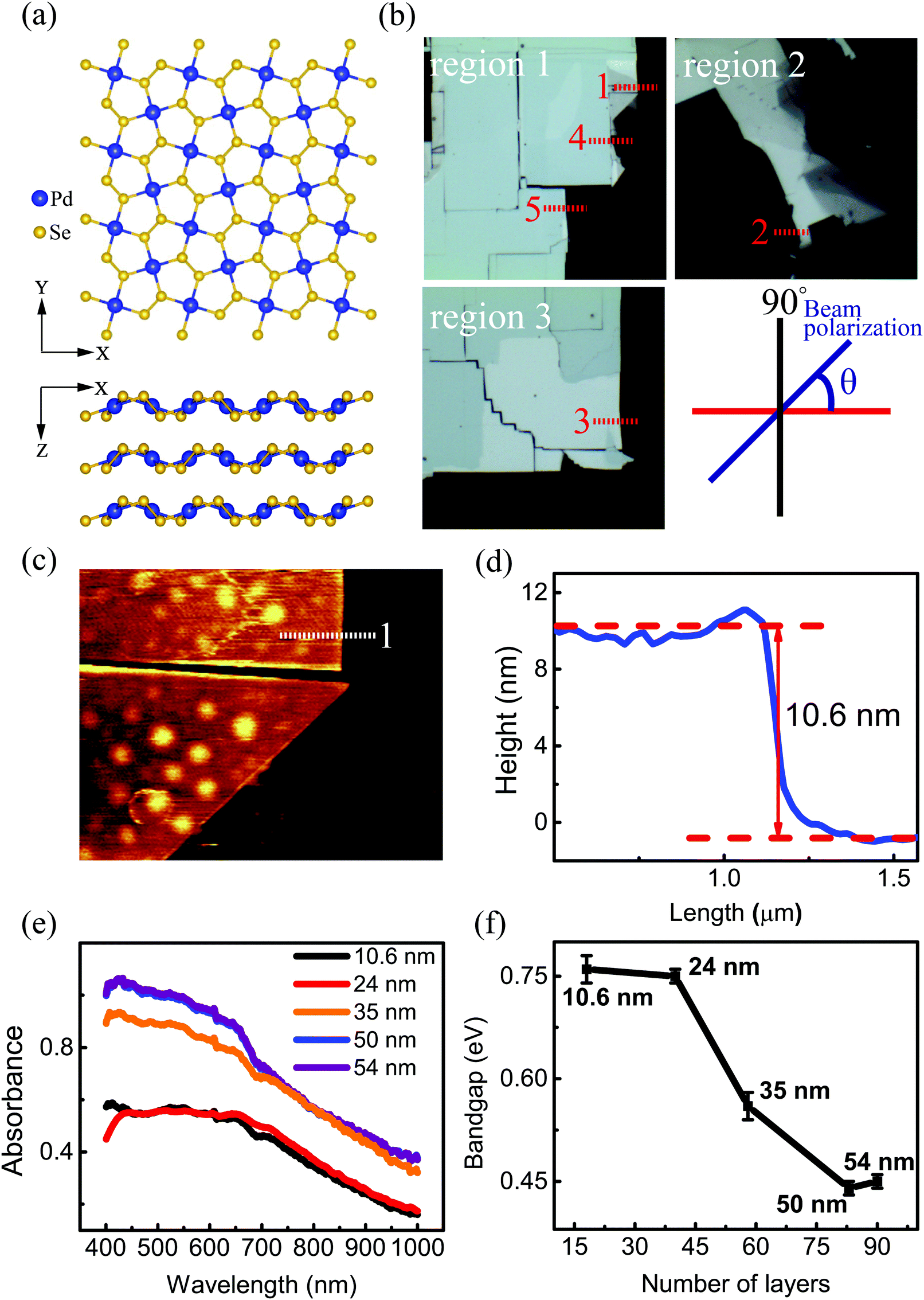 | ||
Fig. 1 Characterization of the PdSe2 flakes. (a) Top and side views of the structure of the puckered PdSe2 crystal. (b) Optical microscope images of exfoliated few-layer PdSe2 flakes on fused quartz, and the numbers 1–5 indicate the order of different thicknesses. All scale bars are 10 μm. (c) Corresponding atomic force microscope (AFM) image corresponding to number 1 in the first image of (b) labeled as region 1. The other two images in (b) are labeled as region 2 and region 3. (d) Corresponding thickness of PdSe2. (e) Absorption spectra of PdSe2 flakes. (f) Thickness-dependent optical band gap extracted from the Tauc plots of  vs. hν for various numbers of PdSe2 layers. vs. hν for various numbers of PdSe2 layers. | ||
To determine the crystal axis of these PdSe2 flakes, we performed polarization-resolved Raman spectra measurements under a parallel configuration (i.e., ei‖es, where ei and es denote the linear polarization of the incident and scattered light, respectively). To do this, we rotated the polarizers in the incident and scattered light paths to change the angle α between the crystallographic orientation and the linear polarization orientation of the incident and scattered light (the blue line shown in Fig. S4, ESI†). The Raman spectrum of 10.6 nm is depicted in Fig. 2. The other Raman spectra are shown in Fig. S3 (ESI†). Four distinct Raman peaks were observed at the wavenumbers of ∼143, ∼206, ∼222, and ∼256 cm−1, which correspond to the A1g–B11g, A2g, B21g, and A3g modes, respectively, which are consistent with previous studies.17,37 The A1g–B11g, A2g, and B21g modes can be attributed to the movement of Se atoms, while the A3g mode (at ∼256 cm−1) represents the relative movement between the Pd and Se atoms. As expected, the Raman peak intensity is strongly dependent on the polarization of the excitation light due to its highly anisotropic optical response. A previous report has shown that the peak intensity of the Ag (B1g) mode oscillates with a periodicity of 180° (90°) as the orientation of the polarization is rotated.37 Using the polar plot of the intensity of the A1g–B11g (∼143 cm−1) mode (see Fig. S4 in the ESI†), it is inferred that the x axis is along the red line (0°), while the y axis is represented by the black line (90°) in Fig. 1(b). This offers a useful approach to determine the crystal orientation of the PdSe2 flakes.
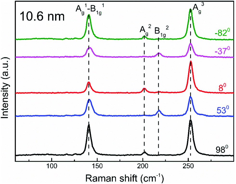 | ||
| Fig. 2 Polarization-dependent Raman spectra of PdSe2 with a thickness of 10.6 nm. Polarization orientations are shown in Fig. S4(d) (ESI†) – see red line (0°) and black line (90°). Raman spectra are shifted vertically for clarity. | ||
To investigate the evolution of the carrier and phonon dynamics with PdSe2 thickness, time-resolved pump–probe TR measurements were performed using a home-built pump–probe system (see Fig. S5 in the ESI†). The TR measurements were carried out via pump excitation using a 520 nm fs pulse and probing with a 1040 nm fs pulse at room temperature. The pump-induced probe reflection change (ΔR) in the PdSe2 flakes can be obtained by chopping the pump using an optical chopper and monitoring the output of the photodiode using a lock-in amplifier (Stanford Research Systems, SR865A). Fig. 3(a)–(e) shows the time-resolved ΔR traces of different PdSe2 regions with a thickness ranging from ∼10.6 nm to ∼54 nm, respectively. The pump and probe beams were polarized along the 0° direction (parallel configuration). A clear negative differential reflection is observed around the zero delay time, which is followed by a rapid ΔR increase and a change to a positive value. Then, the positive differential reflection superimposed with a damped oscillation signal decreases slowly to zero. ΔR < 0 indicates photoinduced bleaching (PB), while ΔR > 0 indicates photoinduced absorption (PA). The damped oscillation reflects the CAP dynamics during the process of charge-carrier recombination in these five regions.
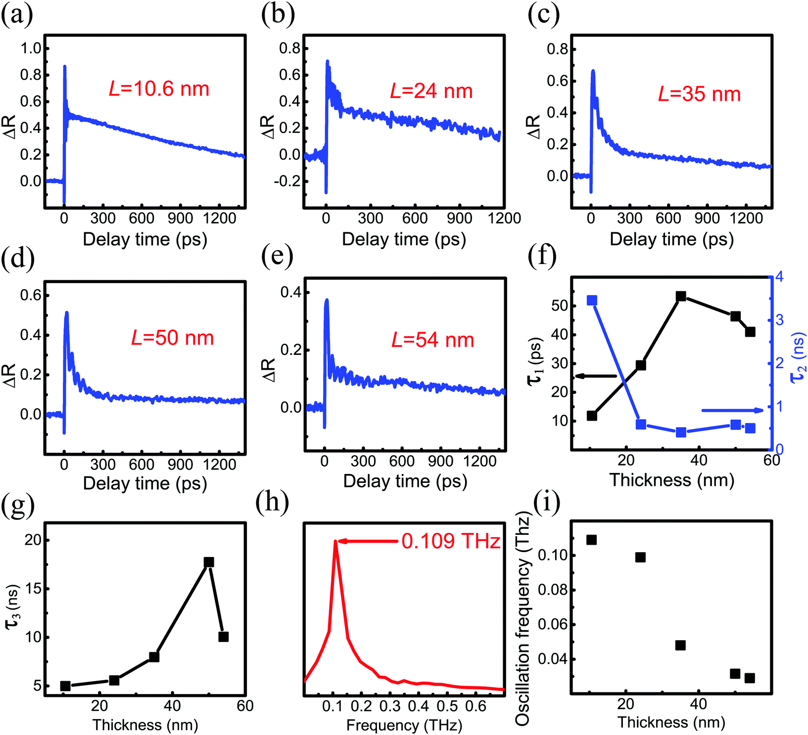 | ||
| Fig. 3 (a–e) Time-resolved TR traces in different PdSe2 regions. The pump (520 nm) and probe (1040 nm) beam fluences were 8 and 4.8 μJ cm−2, respectively. (f and g) Variation of the time constant with the thickness. (h) Fast Fourier transform (FFT) of the oscillations from the TR traces of 10.6 nm. (i) Oscillation frequency vs. PdSe2 thickness. | ||
To determine the relaxation times, we used a semi-log plot to fit the transient curves shown in Fig. 3 for reading the time constants. A tri-exponential decay function plus a damped exponentially attenuated oscillation term is used to fit the measured TR curves.38–40
 | (1) |
The extracted time constants τ1, τ2 and τ3 for different thicknesses are shown in Fig. 3(f) and (g). It is shown that for the 10.6 nm thick region, the relaxation time of the PB signal consists of a fast lifetime τ1 of ∼12 ps, τ2 of ∼3 ns and τ3 of ∼5 ns. For the 24 nm thick region, the relaxation time of the PB signal consists of a fast lifetime τ1 which is increased to ∼29 ps. A non-monotonic change of the fast lifetime τ1 appears for the 35 nm thick region. For the 35 nm, 50 nm and 54 nm thick regions, the fast relaxation time τ1 of the PB signal is 41–53 ps. As the thickness increases (L = 24–54 nm), the slow decay time τ2 decreases sharply and falls in the time range of 0.4–0.6 ns. The regions with thicknesses of 50 and 54 nm show similar relaxation times. The fast recovery time τ1 of the PB signal is ∼46 ps for the 50 nm region. It is very close to the time constant of the 54 nm region (τ1 ≈ 41 ps). The slow decay time for the 50 nm region (τ2 ≈ 0.6 ns) is also close to that of the 54 nm region (τ2 ≈ 0.5 ns). For the 10.6 nm, 24 nm, 35 nm and 50 nm regions, the slow recovery time τ3 increases from ∼5 ns to ∼18 ns. The slow recovery time of the 50 nm region (τ3 ≈ 18 ns) is larger than that of the 54 nm region (τ3 ≈ 10 ns).
The TR curves shown in Fig. 3 indicate that PB around t = 0 s appears for 10.6 nm, 24 nm, 35 nm, 50 nm and 54 nm thick samples of region 1, region 2 and region 3. Furthermore, the increasing time of the signal indicates that thermalization and energy relaxation of hot carriers occurs on a ps time scale in this material. We attributed this fast time constant (τ1) to carrier–carrier and carrier–phonon scattering during the carrier-cooling process. Carrier–phonon scattering causes lattice heating, which sets up a transient stress.41 The TR curves also show that stress-wave-inducing coherent phonon oscillation influences the process of hot carrier cooling. Then, the fast time constant (τ1) of different thicknesses (L = 10.6–54 nm) is of the order of a few dozen picoseconds. The time-resolved ΔR traces of the five thicknesses show that the positive signal returned to equilibrium very slowly. The decay time τ2 for the 10.6 nm think sample was about 3 ns, which is attributed to the interband relaxation time in semiconductors. However, for the 24 nm, 35 nm, 50 nm and 54 nm thicknesses, τ2 decreases dramatically by an order of magnitude to 0.4–0.5 ns. As shown in Fig. 1(f), the band gap indicates a rapid decreasing trend from 24 nm to 50 nm. The band gaps of 50 nm and 54 nm are similar. The slow lifetime τ2 values of 50 nm and 54 nm are very close. It is inferred that the band gap decrease with increasing PdSe2 thickness causes a sharp decrease of the slow decay time τ2 from 10.6 nm (18 layers) to 24 nm (40 layers). Therefore, it is reasonable to deduce that the sudden decrease of the relaxation time indicates the acceleration of the slow interband relaxation process due to band gap narrowing. When the thickness of PdSe2 is larger than 50 layers (30 nm), PdSe2 can be seen as a semi-metal.17,18 For 35 nm, 50 nm and 54 nm, τ2 is nearly thickness-independent. However, the τ2 of PtSe2, which is an analogue of PdSe2, is thickness-dependent.42 The slow lifetime τ3 is attributed to lattice cooling by dissipating the energy to the substrate.43Fig. 3(h) shows the fast Fourier transform (FFT) of the oscillations from the TR traces of the 10.6 nm thick sample (see Fig. S6 for more in ESI†). Fig. 3(i) indicates that the oscillation frequency decreases from 0.109 THz to 29 GHz with the increase of the thickness.
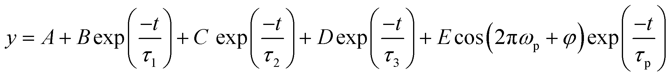
Because PdSe2 exhibits distinct in-plane optical anisotropy due to its unique pentagonal structure, the polarization-resolved measurement of the TR curves in PdSe2 is insightful. For the PdSe2 flake in Fig. 1(b), the TR traces were measured at the D1 region (L = 10.6 nm). This was performed for a series of beam polarization angles θ, ranging from 0° (x axis) to 90° (y axis). The polarization angles of the pump and probe pulses were controlled by rotating half-wave plates and ensuring that they were parallel to each other, as in ref. 44. In this way, we could obtain the carrier dynamics of the PdSe2 flake from the x axis to the y axis. As shown in Fig. 4(a), the negative signals of different angles are almost the same and the maximum values of the positive signals (anti-saturation absorption) increase from 0° to 90°. When the laser polarization approached the 90° direction, the positive signal is maximized, while its normalized decay time indicated no clear change (see Fig. S7 in the ESI†). The respective peak following a sinusoidal dependence on the polarization angle is shown in Fig. 4(b). This can be attributed to pump anisotropic absorption.45
 | ||
| Fig. 4 (a) TR traces, recorded for a series of beam polarizations ranging from 0° to 90°, where the pump and probe polarization directions were parallel to each other. The beam polarization angle is shown in Fig. 1(b). The pump (520 nm) and probe (1040 nm) beam fluences were 8 and 4.8 μJ cm−2, respectively. (b) Peak differential reflection signal as a function of beam polarization angles with respect to sample orientation. | ||
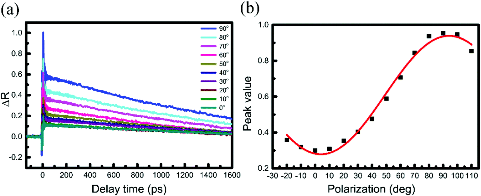
As shown in Fig. 3(a)–(e), CAP oscillations appear in all these measured regions. The amplitude of the oscillation gradually decreases on a long time-scale, which can be attributed to three factors.46–48 One is the process of a pump-induced stress wave, which spreads from the surface to the inner PdSe2, where the absorption of each layer dampens the oscillation. The second factor is that the CAP energy of gradually weakens. The third factor is that the energy of the PdSe2 lattice is gradually dissipated to the substrate and the surrounding environment. The oscillation frequencies were obtained using FFT of the time-resolved traces. Fig. 5(a) shows that the oscillation frequency has no obvious drift with changing laser polarization. This result implies that the oscillation frequency is independent of the pump–probe polarization (parallel configuration). Furthermore, Fig. 5(b) shows that the oscillation period has a linear dependence on the PdSe2 thickness. As shown in Fig. 4(a) and 5(a), although PdSe2 shows different light absorption under different polarizations, the oscillation frequency is independent of the polarization.
 | ||
| Fig. 5 (a) Oscillation frequency as a function of the polarization angle. The oscillation frequency was obtained using the FFT of the TR traces in Fig. 4(a). (b) The oscillation period as a function of the PdSe2 thickness follows a linear fit. (c) CAP oscillation for the 10.6 nm thick sample with different pump fluences. The probe fluence was 4.8 μJ cm−2. (d) Initial amplitude of the coherent acoustic phonon oscillation as a function of the pump power shown in (a). The black dots represent the experimental data, and the red solid line is the linear fit. The right axis is the oscillation frequency for different pump fluences using the FFT. The blue dots represent the experimental data. | ||
The observed oscillating signal should originate from the CAP oscillation, which could induce the reflection change of the time delayed probe via two forms including the photoelastic effect (the dielectric function being modified due to the presence of acoustic strain field, the first term in eqn (2)) and the interferometric effect (CAPs are able to displace surfaces and interfaces, the second term in eqn (2)). For a semi-infinite medium (z = [0, +∞]), the transient differential reflectivity of the probe is written as follows:
 | (2) |
 are the probe light wave vector in a vacuum, the free surface displacement of the sample, the complex optical index, stress and the photoelastic coefficient, respectively.49 According to the signal being linearly dependent on the thickness, this can be attributed to the CAP standing wave. CAP oscillations have previously been studied in GaAs,50 MoS2,41 PtSe2,46 BP,44 and 2H-MoSe2.51 Coherent phonons are phonons that have the same phase when the crystal lattice vibrates. Phonons are divided into acoustic phonons and optical phonons. The acoustic phonon does a centroid motion, that is, each atom in the same unit cell does an overall motion. The optical phonon is a motion with the center of mass unchanged, that is, the relative vibration of different atoms in the unit cell. The acoustic mode can be regarded as a continuous medium elastic wave at low frequency. As previously reported, the pump-induced stress wave interferes with the reflected stress wave in the flakes to form a standing wave.41 One surface of the film is free, but the other is in contact with the hard fused silica. Based on the standing-wave model, the oscillation period (T) can be described via the following formula under an approximately zero-displacement boundary condition:52
 | (3) |
Now, we focus on the generation mechanism of the CAP in our experiment. Two mainstream mechanisms can induce CAP oscillations: the DP and thermoelasticity (TE) mechanisms. For the DP mechanism, the action of light can modify the energy of the electronic distribution in the solid. Since the interatomic forces are indeed completely dependent on the electronic distribution, the action of light can further induce a modification of the interatomic forces via a change of the interactions between cations and electrons, cations and cations and electrons and electrons. Modification of the interatomic forces will result in a variation in the equilibrium position (i.e., deformation occurs) of the lattice and the emission of acoustic phonons. The second mechanism of TE is related to lattice heating and elasticity. Under the action of light, the electrons are excited. The energy of the initially excited electrons is transferred to the phonon sublattice while the non-equilibrium carriers relax to lower energy levels via carrier–phonon scattering, then the lattice is heated. When relaxation processes take place, acoustic phonons are emitted and there is no definite phase relation for these emitted phonons.49
To investigate which mechanism is dominant in our experiment, we performed pump fluence-dependent measurements for the 10.6 nm thick flake. As shown in Fig. 5(c), similar temporal features in TR traces were observed for different pump fluences. Clearly, the amplitude of the CAP oscillations increased gradually with increasing pump fluence. The initial amplitudes of the CAP oscillations were extracted and are shown in Fig. 5(d). Based on the experimental results, it is inferred that the DP mechanism makes the dominating contribution due to the following three reasons:
(1) The measured PdSe2 samples are a semiconductor material and with band gaps larger than 0.44 eV, and the extracted oscillation frequencies range from 29 GHz to 0.109 THz. In solids with a forbidden band, once the electrons in the valence band have been excited by light to the conduction band, the DP mechanism is usually important for roughly 1 GHz to 1 THz frequencies.49
(2) The DP mechanism is efficient for solids in which the lifetime of the photoexcited carriers is longer than the inverse of the CAP cyclic frequency.49 The measured photoexcited carrier lifetime of PdSe2 (larger than 5 ns) is longer than the period of the CAP (smaller than 35 ps). The photoexcited carrier lifetimes of PdSe2 are longer than the period of the CAP oscillations.
(3) As previous reports have shown that the DP-generated CAP oscillation has a typical feature, the initial oscillation amplitude of the coherent acoustic phonon oscillation is proportional to the pump intensity at a relatively low power or fluence.41,44 The measured initial amplitudes of the CAP oscillations of PdSe2 are linearly correlated with the pump power/fluence and the oscillation frequency is independent of the pump power (Fig. 5(d)).
Therefore, the DP mechanism should dominate the CAP generation, and the TE mechanism contributes at longer delay times. In addition, the linear dependence of the initial amplitude vs. the pump power allows us to rule out any significant role played by non-linear two-photon absorption in the transient reflection.
Summary
In summary, the photoexcited carrier dynamics and the CAPs of mechanically exfoliated PdSe2 with different thicknesses were studied via time-resolved pump–probe differential reflection spectroscopy. The carrier dynamics of different thicknesses were investigated using time-resolved pump–probe TR spectroscopy. Polarization-resolved measurement of the TR in PdSe2 reveals the isotropic charge–carrier relaxation dynamics and the CAP frequency in 10.6 nm region. Moreover, the DP mechanism dominates the CAP generation. A sound velocity of 6.78 × 10³ m s−1 was determined based on the oscillation period of the CAP. These new phenomena in thin flakes have many potential applications in optical and THz resonator devices.Experimental section
Sample fabrication and characterization
PdSe2 flakes were fabricated via mechanical exfoliation from the bulk PdSe2 crystal and transferred onto a fused silica substrate (2 mm thickness) using a stock tape. The thickness of the single PdSe2 layer was ∼0.6 nm. The thicknesses of the samples (from 10.6 nm to 54 nm) were measured using atomic force microscopy (Witec Alpha 300) in tapping mode, with 0.1 nm vertical resolution and 8 nm resolution in the transverse direction. Raman spectra were measured with 532 nm laser excitation using the Witec Alpha 300 instrument. The light of the absorption spectra is a halogen lamp. The transmitted light was captured using a microscope objective (100× NA = 0.9) and directed using a spectrometer (PG 2000, Ideaoptics) equipped with a CCD camera (Exmor CMOS Sensor, Sony).Transient reflection measurements
A Yb fiber-based laser (Menlo Systems) was used to provide ultrashort pulses with a central wavelength of 1040 nm and a 100 MHz repetition rate. The pulse width is ∼150 fs. The majority of the output is used as the probe beam and the minority is separated to generate at 520 nm pulse and used as the pump pulse. The probe fluence is attenuated via a combination of a half-wave plate and a Glan Taylor prism. Both the pump pulse and probe pulse were focused into the sample surface with a Gaussian spot, using an objective lens (Tu Plan Fluor 50× NA = 0.8, Nikon). Using this two-color pump–probe setup, the reflected pump beam was stopped from reaching the silicon photodetector using color filters. This significantly improved the signal-to-noise ratio. The reflection change (ΔR) of the probe beam due to the pump excitation was measured using a lock-in amplifier (SR865A, Stanford Research Systems) referenced to 1.5 kHz mechanically chopped pump (SR542, Stanford Research Systems).Author contributions
Z.-B. L., X.-Q. Y. and C.-F. H. conceived the research. C.-F. H. performed the experiments and data analysis. Y.-Z. Z., Q.-N. C., and C.-X. X. measured the absorption spectra. C.-F. H., R. W., X.-Q. Y., D.-K. L., K.-X. H. and Z.-B. L. performed the theoretical analysis. C.-F. H., X.-Q. Y. and Z.-B. L. wrote the manuscript, which all authors read and commented on. Z.-B. L. and J.-G. T. supervised the project.Conflicts of interest
The authors declare no competing financial interest.Acknowledgements
This work was supported by the Natural Science Foundation of China (Grant 11774184, 11974190, and 12074202), and the National Science Foundation of Tianjin (Grant No. 19JCQNJC01800, 18JCZDJC30400 and 20JCQNJC00020).References
- Q. H. Wang, K. Kalantar-Zadeh, A. Kis, J. N. Coleman and M. S. Strano, Nat. Nanotechnol., 2012, 7, 699–712 CrossRef CAS PubMed.
- Y. Chen and M. Sun, Nanoscale, 2021, 13, 5594–5619 RSC.
- J. Fan, J. Song, Y. Cheng and M. Sun, Results Phys., 2021, 24, 104110 CrossRef.
- V. Tran, R. Soklaski, Y. Liang and L. Yang, Phys. Rev. B: Condens. Matter Mater. Phys., 2014, 89, 235319 CrossRef.
- P. Zereshki, Y. Wei, F. Ceballos, M. Z. Bellus, S. D. Lane, S. Pan, R. Long and H. Zhao, Nanoscale, 2018, 10, 11307–11313 RSC.
- H. Liu, A. T. Neal, Z. Zhu, Z. Luo, X. Xu, D. Tománek and P. D. Ye, ACS Nano, 2014, 8, 4033–4041 CrossRef CAS PubMed.
- S. S. Lo, M. S. Devadas, T. A. Major and G. V. Hartland, Analyst, 2013, 138, 25–31 RSC.
- J. Qiao, X. Kong, Z.-X. Hu, F. Yang and W. Ji, Nat. Commun., 2014, 5, 1–7 Search PubMed.
- L. Li, Y. Yu, G. J. Ye, Q. Ge, X. Ou, H. Wu, D. Feng, X. H. Chen and Y. Zhang, Nat. Nanotechnol., 2014, 9, 372 CrossRef CAS.
- A. N. Abbas, B. Liu, L. Chen, Y. Ma, S. Cong, N. Aroonyadet, M. Köpf, T. Nilges and C. Zhou, ACS Nano, 2015, 9, 5618–5624 CrossRef CAS.
- J. O. Island, G. A. Steele, H. S. van der Zant and A. Castellanos-Gomez, 2D Mater., 2015, 2, 011002 CrossRef.
- S. P. Koenig, R. A. Doganov, H. Schmidt, A. Castro Neto and B. Özyilmaz, Appl. Phys. Lett., 2014, 104, 103106 CrossRef.
- J. D. Wood, S. A. Wells, D. Jariwala, K.-S. Chen, E. Cho, V. K. Sangwan, X. Liu, L. J. Lauhon, T. J. Marks and M. C. Hersam, Nano Lett., 2014, 14, 6964–6970 CrossRef CAS PubMed.
- A. Castellanos-Gomez, L. Vicarelli, E. Prada, J. O. Island, K. Narasimha-Acharya, S. I. Blanter, D. J. Groenendijk, M. Buscema, G. A. Steele and J. Alvarez, 2D Mater., 2014, 1, 025001 CrossRef CAS.
- A. Favron, E. Gaufres, F. Fossard, A. L. Phaneuf-L'Heureux, N. Y. Tang, P. L. Levesque, A. Loiseau, R. Leonelli, S. Francoeur and R. Martel, Nat. Mater., 2015, 14, 826–832 CrossRef CAS PubMed.
- W. L. Chow, P. Yu, F. Liu, J. Hong, X. Wang, Q. Zeng, C. H. Hsu, C. Zhu, J. Zhou and X. Wang, Adv. Mater., 2017, 29, 1602969 CrossRef PubMed.
- A. D. Oyedele, S. Yang, L. Liang, A. A. Puretzky, K. Wang, J. Zhang, P. Yu, P. R. Pudasaini, A. W. Ghosh, Z. Liu, C. M. Rouleau, B. G. Sumpter, M. F. Chisholm, W. Zhou, P. D. Rack, D. B. Geohegan and K. Xiao, J. Am. Chem. Soc., 2017, 139, 14090–14097 CrossRef CAS PubMed.
- L.-H. Zeng, D. Wu, S.-H. Lin, C. Xie, H.-Y. Yuan, W. Lu, S. P. Lau, Y. Chai, L.-B. Luo, Z.-J. Li and Y. H. Tsang, Adv. Funct. Mater., 2019, 29, 1806878 CrossRef.
- J. Yu, X. Kuang, Y. Gao, Y. Wang, K. Chen, Z. Ding, J. Liu, C. Cong, J. He and Z. Liu, Nano Lett., 2020, 20, 1172–1182 CrossRef CAS PubMed.
- Q. Liang, Q. Wang, Q. Zhang, J. Wei, S. X. Lim, R. Zhu, J. Hu, W. Wei, C. Lee and C. Sow, Adv. Mater., 2019, 31, 1807609 CrossRef.
- M. Long, Y. Wang, P. Wang, X. Zhou, H. Xia, C. Luo, S. Huang, G. Zhang, H. Yan, Z. Fan, X. Wu, X. Chen, W. Lu and W. Hu, ACS Nano, 2019, 13, 2511–2519 CAS.
- J. Zhong, J. Yu, L. Cao, C. Zeng, J. Ding, C. Cong, Z. Liu and Y. Liu, Nano Res., 2020, 13, 1780–1786 CrossRef CAS.
- W. Xu, J. Jiang, H. Ma, Z. Zhang, J. Li, B. Zhao, R. Wu, X. Yang, H. Zhang, B. Li, W. Shu, Z. Zhang, B. Li, Y. Liu, L. Liao and X. Duan, Nano Res., 2020, 13, 2091–2097 CrossRef CAS.
- D. Wu, J. Guo, J. Du, C. Xia, L. Zeng, Y. Tian, Z. Shi, Y. Tian, X. J. Li, Y. H. Tsang and J. Jie, ACS Nano, 2019, 13, 9907–9917 CrossRef CAS PubMed.
- A. M. Afzal, G. Dastgeer, M. Z. Iqbal, P. Gautam and M. M. Faisal, ACS Appl. Mater. Interfaces, 2020, 12, 19625–19634 CrossRef CAS PubMed.
- D. Wu, C. Jia, F. Shi, L. Zeng, P. Lin, L. Dong, Z. Shi, Y. Tian, X. Li and J. Jie, J. Mater. Chem. A, 2020, 8, 3632–3642 RSC.
- Y. Ma, S. Zhang, S. Ding, X. Liu, X. Yu, F. Peng and Q. Zhang, Opt. Laser Technol., 2020, 124, 105959 CrossRef CAS.
- L. H. Zeng, Q. M. Chen, Z. X. Zhang, D. Wu, H. Yuan, Y. Y. Li, W. Qarony, S. P. Lau, L. B. Luo and Y. H. Tsang, Adv. Sci., 2019, 6, 1901134 CrossRef CAS PubMed.
- D. Li, J. Fu, P. Suo, W. Zhang, B. Lu, X. Lin, X. Yan, B. Li, G. Ma and J. Yao, Appl. Phys. Lett., 2021, 118, 191105 CrossRef CAS.
- T. V. Alencar, M. G. Silva, L. M. Malard and A. M. de Paula, Nano Lett., 2014, 14, 5621–5624 CrossRef CAS PubMed.
- H. Wang, C. Zhang and F. Rana, Nano Lett., 2015, 15, 339–345 CrossRef CAS PubMed.
- C. Soulard, X. Rocquefelte, P. E. Petit, M. Evain, S. Jobic, J. P. Itié, P. Munsch, H. J. Koo and M. H. Whangbo, Inorg. Chem., 2004, 43, 1943–1949 CrossRef CAS.
- J. Lin, S. Zuluaga, P. Yu, Z. Liu, S. T. Pantelides and K. Suenaga, Phys. Rev. Lett., 2017, 119, 016101 CrossRef.
- A. P. Alexander, D. O. Akinola, X. Kai, V. H. Amanda, G. S. Bobby, M. David, B. G. David and L. Liangbo, 2D Mater., 2018, 5, 035016 CrossRef.
- J. Tauc, R. Grigorovici and A. Vancu, Phys. Status Solidi B, 1966, 15, 627–637 CrossRef CAS.
- G. Zhang, M. Amani, A. Chaturvedi, C. Tan, J. Bullock, X. Song, H. Kim, D.-H. Lien, M. C. Scott and H. Zhang, Appl. Phys. Lett., 2019, 114, 253102 CrossRef.
- A. P. Alexander, D. O. Akinola, X. Kai, V. H. Amanda, G. S. Bobby, M. David, B. G. David and L. Liangbo, 2D Mater., 2018, 5, 035016 CrossRef.
- A. Yamamoto, T. Mishina, Y. Masumoto and M. Nakayama, Phys. Rev. Lett., 1994, 73, 740–743 CrossRef CAS PubMed.
- J. Miller, J. Qi, Y. Xu, Y.-J. Cho, X. Liu, J. Furdyna, I. Perakis, T. Shahbazyan and N. Tolk, Phys. Rev. B: Condens. Matter Mater. Phys., 2006, 74, 113313 CrossRef.
- Y. Xu, J. Qi, J. Miller, Y. J. Cho, X. Liu, J. Furdyna, T. Shahbazyan and N. Tolk, Phys. Status Solidi C, 2008, 5, 2632–2636 CrossRef CAS.
- S. Ge, X. Liu, X. Qiao, Q. Wang, Z. Xu, J. Qiu, P. H. Tan, J. Zhao and D. Sun, Sci. Rep., 2014, 4, 5722 CrossRef CAS PubMed.
- X. Zhao, F. Liu, D. Liu, X.-Q. Yan, C. Huo, W. Hui, J. Xie, Q. Ye, C. Guo and Y. Yao, Appl. Phys. Lett., 2019, 115, 263102 CrossRef.
- Q. Cui, F. Ceballos, N. Kumar and H. Zhao, ACS Nano, 2014, 8, 2970–2976 CrossRef CAS PubMed.
- S. Meng, H. Shi, H. Jiang, X. Sun and B. Gao, J. Phys. Chem. C, 2019, 123, 20051–20058 CrossRef CAS.
- L. Pi, C. Hu, W. Shen, L. Li, P. Luo, X. Hu, P. Chen, D. Li, Z. Li and X. Zhou, Adv. Funct. Mater., 2021, 31, 2006774 CrossRef CAS.
- X. Chen, S. Zhang, L. Wang, Y.-F. Huang, H. Liu, J. Huang, N. Dong, W. Liu, I. M. Kislyakov and J. M. Nunzi, Photonics Res., 2019, 7, 1416–1424 CrossRef CAS.
- C.-K. Sun, Y.-K. Huang, J.-C. Liang, A. Abare and S. P. DenBaars, Appl. Phys. Lett., 2001, 78, 1201–1203 CrossRef CAS.
- D. Lim, R. D. Averitt, J. Demsar, A. J. Taylor, N. Hur and S. W. Cheong, Appl. Phys. Lett., 2003, 83, 4800–4802 CrossRef CAS.
- P. Ruello and V. E. Gusev, Ultrasonics, 2015, 56, 21–35 CrossRef CAS PubMed.
- Y. Xu, J. Qi, J. Miller, Y. J. Cho, X. Liu, J. K. Furdyna, T. V. Shahbazyan and N. Tolk, Phys. Status Solidi C, 2008, 5, 2632–2636 CrossRef CAS.
- P. Soubelet, A. A. Reynoso, A. Fainstein, K. Nogajewski, M. Potemski, C. Faugeras and A. E. Bruchhausen, Nanoscale, 2019, 11, 10446–10453 RSC.
- C. Thomsen, J. Strait, Z. Vardeny, H. J. Maris, J. Tauc and J. Hauser, Phys. Rev. Lett., 1984, 53, 989 CrossRef CAS.
- Z. Huang, W. Zhang and W. Zhang, Materials, 2016, 9, 716 CrossRef PubMed.
Footnote |
| † Electronic supplementary information (ESI) available: AFM results, bandgap extraction, polarization-dependent Raman spectra, anisotropy in the Raman intensity, schematic diagram of experimental setup, the curves of the FFT, polarization dependence of normalized curves. See DOI: 10.1039/d1cp03202j |
| This journal is © the Owner Societies 2021 |