
2D ferroelectric devices: working principles and research progress
Minghao
Liu
a,
Ting
Liao
a,
Ziqi
Sun
b,
Yuantong
Gu
 *a and
Liangzhi
Kou
*a
*a and
Liangzhi
Kou
*a
aSchool of Mechanical, Medical and Process Engineering, Queensland University of Technology, Brisbane, QLD 4001, Australia. E-mail: liangzhi.kou@qut.edu.au; yuantong.gu@qut.edu.au
bSchool of Chemistry and Physics, Queensland University of Technology, Brisbane, QLD 4001, Australia
First published on 18th August 2021
Abstract
Two-dimensional (2D) ferroelectric materials are promising for use in high-performance nanoelectronic devices due to the non-volatility, high storage density, low energy cost and short response time originating from their bistable and switchable polarization states. In this mini review, we first discuss the mechanism and operation principles of ferroelectric devices to facilitate understanding of these novel nanoelectronics and then summarize the latest research progress of electronic devices based on 2D ferroelectrics. Finally, the perspectives for future research and development directions in various fields are provided. We expect this will provide an overview regarding the application of 2D ferroelectrics in electronic appliances.
Introduction
Ferroelectrics are materials with ordered spontaneous polarization that can be re-oriented under an external electric field. The bistable and switchable polarization states originate from their spatial symmetry breaking and offset negative/positive charge centre which have been explored to design functional devices,1–4 such as sensors, ferroelectric-field effect transistors (FeFET), and ferroelectric tunnel junctions (FTJ) (Fig. 1). Compared with traditional devices based on common semiconductors/insulators, the ferroelectric devices show obvious advantages such as low energy consumption, high response speed and non-volatility.5–7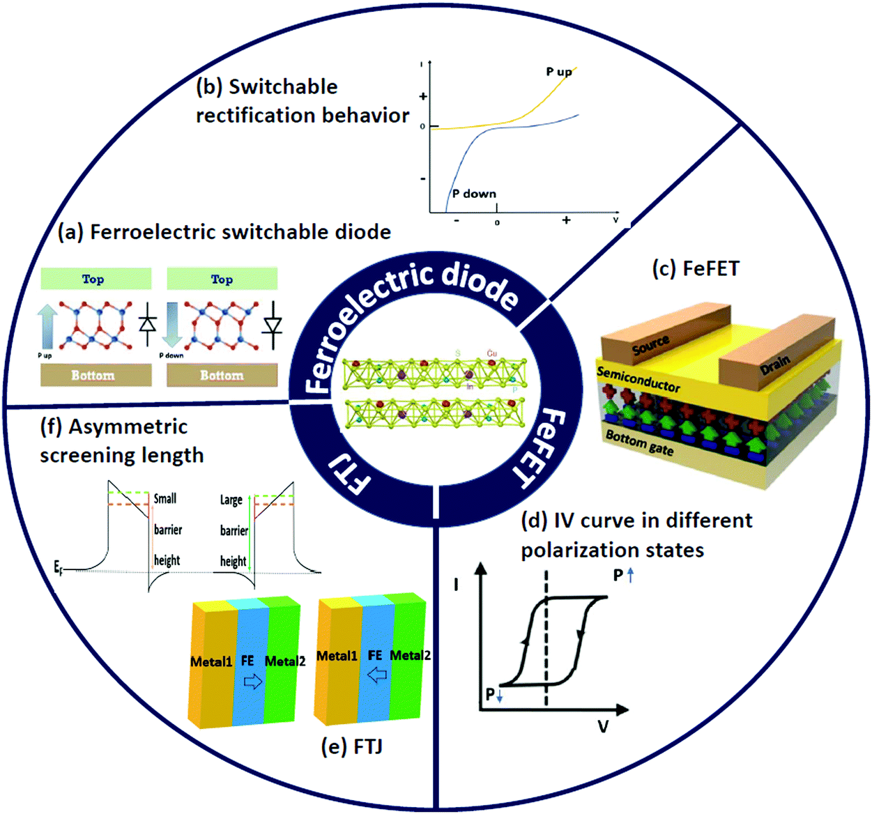 | ||
| Fig. 1 Ferroelectric material devices (reprinted with permission from ref. 16, copyright 2016 Springer Nature) and their main applications. (a) Schematic diagram of ferroelectric switchable diode. (b) I–V curve of ferroelectric diode with switchable rectification behaviour. (Fig. 1(a and b) reproduced from ref. 40 with permission from The Royal Society of Chemistry.) (c) Schematic diagram of FeFET structure. (d) Current–voltage curves in different polarization states. (Fig. 1(c and d) reprinted with permission from ref. 41, copyright 2021 AIP Publishing.) (e) Schematic diagram of FTJ structure. (f) The formation mechanism of FTJ. (Fig. 1(e and f) reprinted with permission from ref. 42, copyright 2016 Springer Nature.) | ||
Over the last decades, research on ferroelectrics has mainly focused on traditional three-dimensional (3D) perovskites with the chemical formula of ABO3. They have been proposed for the fabrication of ferroelectric devices and great successes have been achieved at the laboratory level.8,9 However, their practical applications are still hindered by intrinsic issues including depolarization and structural instabilities when the thickness is reduced to atomic scale due to surface reconstruction and dangling bonds. A significant drop in the Curie temperature, or even the disappearance of ferroelectricity,10–12 is the biggest obstruction toward real and large-scale applications. Therefore, a nanomaterial with high structural and ferroelectric stabilities is crucial to developing functional electronic devices.
Graphene13 and other 2D materials14–16 have emerged in recent years to provide feasible solutions for the dilemma due to their excellent optical,17 electrical,18,19 thermal,20 mechanical and ferroelectric properties21 that do not exist in bulk materials. In particular, 2D ferroelectric materials with clean surfaces and stable polarization are promising for electronic device applications.22 Currently, around 13 2D ferroelectrics have been experimentally confirmed and more than 100 candidates have been theoretically predicted,22 including group IV monochalcogenides,23 monolayer transition metal dichalcogenides,24 and group III–V binary compounds.22,25–28 The successful synthesis of 2D ferroelectrics, explicit the demonstration of ferroelectricity and the effective manipulations of ferroelectric switching render the application of new ferroelectric devices feasible.29,30
In this mini review, we briefly introduce the working mechanism of ferroelectric devices and summarize the current research progress of devices based on 2D ferroelectrics; an outlook on the future trends in ferroelectric electronic applications is discussed at the end of the review.
Working mechanism and research progress of 2D ferroelectric devices
Fundamentally speaking, switchable polarization under external stimuli, the unique feature of ferroelectric materials, is the underlying principle and mechanism for all ferroelectric devices.6,31–33 Although the bi-stable and switchable polarization states can be simply regarded as logic 0 or 1, as pointed out in some literature,34–36 data storage and logic processes based on the polarization states are still challenges in reality, due to the manipulation difficulties of reading and writing.37 More commonly, the architectures of traditional electronic devices (like FET and FTJ) are still adopted in ferroelectric devices, but the polarization states of ferroelectrics, rather than the external bias, are introduced as the effective approach to switch ON/OFF the conducting channels by changing the carrier concentrations or band bending, as seen in Fig. 1. Due to the switchability and bistability of the polarization states, ferroelectric devices possess the advantages of fast writing speed, low energy consumption and non-volatility.38,39 In these devices, ferroelectrics are the core materials that achieve the designed functionalities.30 For example, ferroelectric polarization can rectify the current, which is key to achieving bidirectional rectification behaviour in ferroelectric diodes (Fig. 1a and b).40 The two stable polarization states in ferroelectrics can be reversed under an external field to store digital information and are responsible for the non-volatility of FeFET (Fig. 1c and d).41 Meanwhile, polarization reversal in the ferroelectric heterostructure can change the electron tunnelling transmittance and resistive switching; a FTJ42 can thus be designed based on the quantum tunnelling effect43 and different screening lengths44 (Fig. 1e and f). In the following, these three representative 2D ferroelectric nanodevices, namely the ferroelectric field-effect transistor, diode, and tunnelling junction (see Fig. 1), are presented with more detailed working principles and their research progress.Ferroelectric field-effect transistor (FeFET)
2D ferroelectric field-effect transistors (FeFET) are the typical devices that utilize a ferroelectric switch to control the conducting channel and achieve ON/OFF states.45–47 FeFETs generally adopt the same architectures as their traditional predecessors but control the conductance of the channel via polarization rather than an external electric field.48 Taking the n-type traditional FETs as an example, the electric channel is switched off due to carrier depletion between the source and the drain of the PN junction. The energy band between the insulating layer and the semiconductor layer bends under a positive voltage. When the edge of the conduction band bends below the Fermi level of the semiconductor, electrons can move through to turn on the channel. A very similar principle is applied for FETs with p-type semiconductors. The valence band of the FeFET bends upward when a negative voltage is applied. A channel composed of holes is formed in the source and drain electrodes and the device becomes conductive. The underlying principle is still valid49 in FeFETs, although a ferroelectric dielectric layer is inserted between the semiconductor and the bottom gate (Fig. 2a). However, due to the ferroelectricity and remanent polarization Pr, the channel state in FeFETs can be maintained even if the applied voltage is removed, leading to non-volatility.41 The reserved state (ON/OFF state of the channel) disappears only when the negative voltage exceeds the coercive field Ec and is large enough to induce a change in the ferroelectric polarization direction. | ||
| Fig. 2 (a) Schematic diagram of the structures of FeFET and FeSFET. (Reprinted with permission from ref. 41, copyright 2021 AIP Publishing.) (b) Schematic diagram of the structure of a two-dimensional ferroelectric field-effect heterojunction transistor. (c and d) PFM amplitude and phase image of a vdW heterostructure. (e) The I–V curve under various gate voltages. (f) The dynamic characteristics of FeFET in response to a periodic pulse. (g) Endurance test, measuring the current curve under alternating program and erase cycles. (h) The retention time performance test curve. (Reprinted with permission from ref. 53, copyright: 2016 Springer Nature.) | ||
Although the concept of FeFETs was first proposed in 1957,50 devices based on 2D ferroelectric materials have been realized only very recently. In 2016, Liu et al. observed 2D ferroelectricity in CuInP2S6 (CIPS) ultrathin film with a thickness of around 4 nm through piezoelectric force microscopy (PFM) and second-harmonic generation (SHG), which opened the avenue of using 2D ferroelectrics for transistors.16 For example, Si et al. used CulnP2S6 as the gate and MoS2 as the channel to build a 2D van der Waals heterojunction as an FeFET. The 2D CIPS & MoS2 have no dangling bonds in the interlayer and the on/off ratio is as high as 104, which can keep it stable under atmospheric environments. The observed counter-clockwise hysteresis loop at room temperature demonstrated the stabilities of the ferroelectricity and the designed device.45 Alternatively, Wan et al. combined α-In2Se3 (as the insulator gate) with graphene (as the channel) to design a FeFET. Its stable out-of-plane ferroelectricity was also observed at room temperature, while the measured ON/OFF ratio reached 105. These pioneering works prove that 2D ferroelectric materials have good application prospects in electronics.51
Although the FeFETs based on 2D ferroelectrics are quite promising for new generation transistors with high stability and ON/OFF ratios, the path towards real applications is still hindered by factors like the short retention time that results from gate current leakage and charge trapping52,53 at the interface of the semiconductor and the ferroelectrics. In order to address this issue, a new device, a ferroelectric semiconductor field-effect transistor (FeSFET), was recently proposed (Fig. 2a). In a FeSFET, the ferroelectric material is used as the semiconducting layer, while a higher quality amorphous insulating material is used as the insulating layer (Fig. 2b). In this structure, the depolarization field that appears in the traditional semiconductor layer can be eliminated by mobile electrons. This structural change has brought a fundamental change in the working mechanism of the FeSFET.54 In a FeFET, the electrostatic potential is affected only by the polarization of the gate insulator and the semiconductor interface. However, the drain current in a FeSFET is determined by the upper and lower surfaces of the semiconductor since the polarized charges can be collected on the upper and lower surfaces of the semiconductor. This novel design has been demonstrated to significantly improve the performance of the device.53 More importantly, charge trapping can be effectively reduced or even eliminated in van der Waals structures. It can be seen from Fig. 2c and d that the domain size of the ferroelectric materials on h-BN or MoS2 is much smaller than that on graphene. The performance of the FeSFET, such as the memory window and retention time, can be thus greatly improved in the van der Waals structure. The new FeSFET and its principles have been demonstrated by Si et al., who effectively increased the retention time. The architecture uses ferroelectric indium selenide (α-In2Se3) as the channel material and HfO2 as the gate insulator. The switching performance of the new FeSFET, namely the ON/OFF ratio, can reach up to 108. More importantly, it has a maximum drain current of 671 μA μm−1 with a large memory window and low voltage requirements.54 In 2021, Wang et al. further improved the FeFET by adopting the metal–ferroelectric–metal–insulator–semiconductor architecture, where MoS2 and CulnP2S6 heterojunctions were used as channel materials, graphene as the gate contact, and hexagonal-BN as the gate dielectric (Fig. 2b). Due to the effective charge-trapping, the retention time is greatly increased to 10 years. Moreover, it has a memory window of 3.8 V (Fig. 2e) and an ON/OFF ratio over 107. The device can complete the plane reversal within 100 ns (Fig. 2f).53 With the development of 2D FeFET, the gap between the prototype device and its practical application is quickly decreased, as digital information can be programmed and erased (Fig. 2g and h).
In addition to the common transistor application discussed above, the low-consumption and high-density integration characteristics of 2D ferroelectrics can also be used for promising neurosynaptic devices. For instance, Kwon et al. designed a Pt/SnS/Pt synaptic device in which the 2D in-plane ferroelectric material SnS acts as the channel material and the multilevel conductance state can be locally switched by controlling the ferroelectric domains of SnS. At a thickness of 6 nm, the simulation accuracy reached 92.1%. Significantly, the device reached an ON/OFF ratio of 104, can operate stably at room temperature and does not require any passivation.55 Besides the in-plane ferroelectrics, a nerve protruding device based on 2D ferroelectrics with out-of-plane polarization was also recently designed by Gao et al.56 In addition to the typical behaviours of nerve protrusion, such as paired-pulse facilitation, long-term plasticity and short-term plasticity, the memory reinforcement engineering of the mammalian brain was simulated successfully. This research progress not only indicates the promising future of 2D ferroelectrics for FeFETs, but also their bright future in neurosynaptic devices.
Ferroelectric switchable diode
A diode57–59 is another representative device in which ferroelectric materials can be used to rectify the current behaviour and the performance can be significantly improved based on the unique polarization feature. Different from traditional unidirectional rectifier diodes, ferroelectric semiconductors57 can change the rectification direction of the device according to the polarity switching of the ferroelectric material (Fig. 3a).40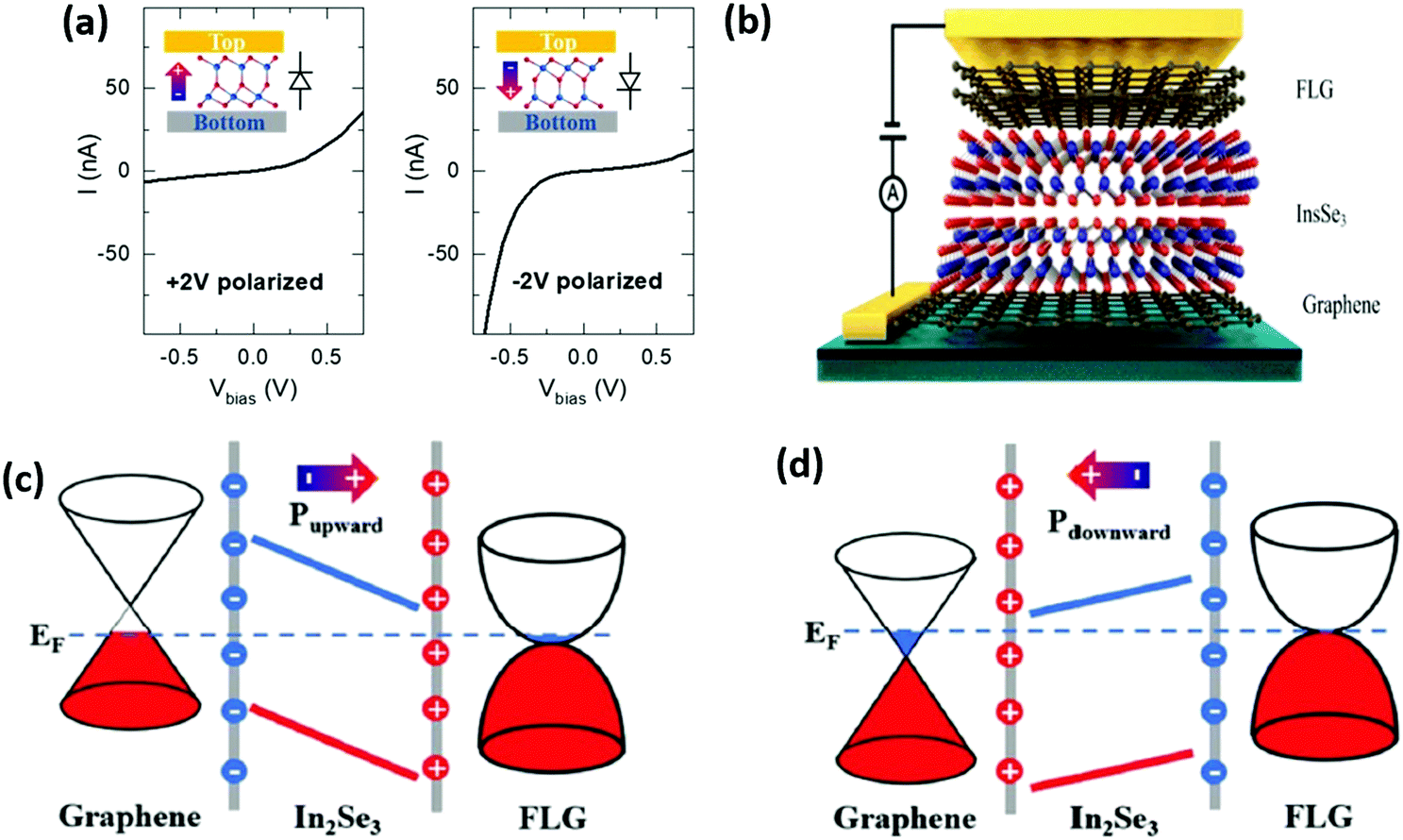 | ||
| Fig. 3 (a) Schematic diagram of ferroelectric adjustable diode structure. (b) I–V curve of diode rectification function. (c and d) Explanation of the switchable rectification behaviour of a ferroelectric diode, showing the energy band diagram of the graphene/In2Se3 heterostructure and the evolution of the Schottky barrier in the ferroelectric polarization reversal. (Reproduced from ref. 40 with permission from The Royal Society of Chemistry.) | ||
This unique behaviour of ferroelectric diodes is due to the modification of the Schottky barrier60,61 by two mechanisms: (1) the reversal of the polarization in ferroelectric material can cause a change of internal electric field, which leads to a drastic potential change relative to the vacuum level on both sides. (2) The materials on both sides of the ferroelectric diode differ in their ability to induce screening charges.40
Fig. 3b is a schematic diagram of a heterojunction ferroelectric diode, in which few-layer graphene (FLG) and monolayer graphene are the top electrode and bottom electrode, respectively. The Schottky barrier at the α-In2Se3/FLG interface is much lower than that at the bottom α-In2Se3/graphene interface due to the presence of polarization. Therefore, the diode is conductive from α-in2Se3 to the FLG electrode. When a forward voltage is applied, the Schottky barrier is increased at the bottom but reduced at the top, strengthening the diode's rectification effect. In the case of a negative voltage, the internal electric field of the ferroelectric material changes, strongly suppressing the Schottky barrier at the bottom and strengthening the Schottky barrier at the top.40 Thus, a reverse rectification behaviour can be observed, as seen in Fig. 3c and d.
A similar ferroelectric diode was also fabricated based on a van der Waals (vdW) ferroelectric CIPS/Si heterostructure, in which the CuInP2S6 (CIPS) ultrathin film has a thickness of around 4 nm, and good memory behaviour with an ON/OFF ratio of ∼100 was measured. This appealing work opened a novel avenue for 2D ferroelectrics-based devices.16 Another ferroelectric diode with similar architecture was built by Wan et al. and was composed of a graphene/α-In2Se3 heterojunction structure. The 5 nm thick In2Se3 film can maintain stable out-of-plane ferroelectricity at room temperature, with an ON/OFF ratio of 105 and a low coercive electric film requirement of 2 × 10⁵ V cm−1.
Ferroelectric tunnel junction (FTJ)
The ferroelectric tunnel junction is a device based on the quantum-mechanical tunnelling that occurs when the thickness of the ferroelectric layer is reduced to nanoscale. They are generally smaller in size than ferroelectric capacitors, but have a higher readout speed than ferroelectric diodes.44,62,63 A FTJ has a sandwich structure64,65 with a semiconductor or metal as the leads and a ferroelectric material as the central tunnel barrier (Fig. 1e). The main parameter to measure the performance is the tunnelling electroresistance66–68 (TER) which is contributed by the different screening capabilities of the leads on opposite sides of the ferroelectric material and the asymmetric potential profile from the polarization charge effect (Fig. 1f).42,44 Depending on voltage and thickness, different transmission mechanisms are responsible for the tunnel currents. For example, direct tunnelling predominates in low voltage and thin thickness and is generally the main mechanism in FTJ, while Fowler–Nordheim tunnelling is responsible under higher voltage (Fig. 4a).65 The mechanism changes with the thermionic emission when the thickness increases. Additionally, the transport resistance is related to the ferroelectric domain population (Fig. 4b).69 Therefore, the ON/OFF signal can be outputted in FTJs with respect to the ferroelectric polarized states (Fig. 4c).70 | ||
| Fig. 4 (a) Three transport mechanisms in nano-level ferroelectrics: direct tunnelling (DT), Fowler–Nordheim tunnelling (FNT) and thermionic emission. (Reprinted with permission from ref. 65, copyright 2010 American Physical Society.) (b) The correlation between resistance and the corresponding proportion of polarization reversal. (Reprinted with permission from ref. 69, copyright 2013 American Physical Society.) (c) The transmission and TER ratio as a function of electron energy in both polarization states. (d) The structure of FTJ with electron injection and transmitting process. (e) PDOS chart comparison: pristine In2Se3, P upstate, P downstate, and in contact with Au, respectively. (Reprinted with permission from ref. 63, copyright 2020 American Physical Society.) | ||
A large TER is essential for a FTJ as an electronic device being applied in practice; the performance can be improved via modulating the screening ability of the lead.71–73 Alternative strategic approaches to improve the TER have been also proposed in recent years. For instance, the TER ratio can be increased by phase transition at the insulator/metal interface as a result of ferroelectric polarization70,74 or the consumed or accumulated charge carriers at the interface.75 Doping is thus an effective alternative strategy to increase the TER and ON/OFF ratios of 2D FTJ,64,76 since both the barrier height and width of the semiconductor surface can be dynamically modulated due to the doping-induced change of the majority carriers according to the ferroelectric switching. Recently, surface functionalization of 2D materials was proposed to induce ferroelectricity and improve the TER.77 The ferroelectric/non-ferroelectric junction can be theoretically designed by passivating germanene with –CH3 and CH2F.78 In contrast to ferroelectric transistors, both in-plane and out-of-plane ferroelectric materials can be used to design ferroelectric tunnel junctions. As an example,79 in-plane polarization of 2D ferroelectrics leads to upward or downward band bending of the interface, depending on the polarization direction, which can then change the resistance and modulate the barrier widths, thereby achieving a large TER. For out-of-plane ferroelectric materials, the working mechanism of the FTJ is similar,78 but depends on the work functions of the two surfaces of the ferroelectrics. When the work functions at the opposite surfaces are similar/close, the 2D polar materials will remain insulated. In contrast, when the work functions are significantly different because of ferroelectric polarization, the empty conduction band or the full valence band will be filled due to charge transfer and the conducting channel will be switched on. Therefore, a two-dimensional ferroelectric material can act as the switcher to control the ON/OFF state of the channel and achieve the TER effect.63
Based on these working principles and the developments in 2D ferroelectric materials, a large number of 2D FTJs have been either theoretically proposed or experimentally designed. For example, Kang et al. proposed an FTJ based on a 2D ferroelectric BiP with in-plane ferroelectricity in which B/N-doped graphene is used as the leads. In theoretical simulations, the TER ratio can reach up to 623%, which proves the feasibility of fabricating a heterojunction based on 2D ferroelectrics.80 Rather than a complicated heterostructure of combined different materials, Shen et al. designed a novel in-plane 2D ferroelectric tunnel homojunction by a simple doping strategy. The opposite ends of the ferroelectric SnSe monolayer are doped with In and Sb, which covert them into p-type and n-type semiconductors, respectively. A device composed of p-type semiconductor/ferroelectric/n-type semiconductor structure was thus designed. The in-plane ferroelectricity is helpful to maintain stability in a single-layer ferroelectric tunnel junction of atomic thickness. As estimated from a density functional theory simulation, the TER effect can reach 1460%.64
Different from the strategies to achieve a high TER ratio by using asymmetric left and right leads and different screening lengths, a much higher TER ratio can be achieved through metallic–insulating change under reversible polarization. For instance, due to the change of work function and charge transfer between graphene and the ferroelectric In2Se3 monolayer, the system can be metallic or insulating depending on the polarization direction. Kang et al. thus proposed a 2D FTJ based on the ferroelectric heterojunctions of In2Se3 and graphene, realizing a significant TER ratio of 108%63 which exceeds the value of most 3D ferroelectric heterojunctions. When the In2Se3 layer is replaced with an Au(010) surface (Fig. 4d), the contact method can be changed from ohmic to Schottky type by the polarization direction due to the difference in work functions on the two polar surfaces of In2Se3 and the subsequent substantially different charge transfer between Au(010) and In2Se3. Through PDOS analysis, it can be seen that in polarization upstate, In2Se3 is still a semiconductor, while in polarization downstate, In2Se3 becomes metallic (Fig. 4e). As a result, greatly different equilibrium tunnel conductances dependent on the ferroelectric polarization can be obtained; the corresponding TER reaches up to 104%.70 The outstanding performance of the 2D ferroelectrics-based heterojunction and device indicates that it is promising and feasible to develop FTJs based on 2D ferroelectrics.
In recent years, there has also been significant experimental progress in FTJ investigations which effectively demonstrated working principles and theoretical predictions. Based on the atomic-thickness in-plane 2D ferroelectric SnTe, which can maintain robust ferroelectricity at room temperature at a thickness of 2–4 unit cells, a protype FTJ device for non-volatile ferroelectric random access memory was fabricated and a high ON/OFF ratio of 3000 in 3-unit cell film was achieved as a result of band bending.81 In 2019, by using a 2D distorted ferroelectric 1T-MoTe2 monolayer which exhibits room temperature ferroelectricity, Yuan et al. fabricated a 2D vdW d1T-MoTe2/graphene FTJ device which demonstrated an ON/OFF resistance ratio of 1000.82
Summary and outlook
Due to their high structural and ferroelectric stability, 2D ferroelectrics with switchable polarization have become potential candidates in the fields of artificial intelligence, information processing, and memory.83 This mini review summarizes the optimization operating mechanism of three representative ferroelectric devices, including FeFET, ferroelectric diode, and FTJ. Great achievements have been made over the last few years: devices based on 2D ferroelectrics generally possess improved ON/OFF ratios, long retention time, low energy cost, non-volatility and fast operation speed when compared with traditional devices, although they share similar architectures. The obvious advantages of ferroelectric devices have inspired the academic and industrial communities, but great challenges have to be overcome before their practical application.The first challenge is the 2D ferroelectric material itself. The lack of 2D ferroelectric materials with high stability and excellent performance is one of the main roadblocks restricting the development of corresponding devices. Although more than 10 2D ferroelectric materials have been experimentally synthesized in which the ferroelectricity was explicitly demonstrated, like CIPS,16 In2Se328,84 and SnS,23,85,86 there are still very limited choices of materials for ferroelectric device fabrication. 2D ferroelectrics with higher Curie temperature, stronger polarization and better structural stability are urgently needed to improve the performance of the corresponding devices. Janus materials, such as B2P6, with intrinsic polarization are possible candidates to replace 2D ferroelectrics for device applications,87 although comprehensive investigations are still required based on the characterization and fabrication technology,88 such as PFM89–91 and SHG.92,93
The second challenge is a thorough understanding of the underlying mechanism.94,95 As briefly reviewed above, although it is basically clear that the working mechanism is a polarization-controlled ON/OFF channel due to band bending, carrier density variations and changes of contact types, some effects, like those of channel length, interface interaction and polarization strength/reversal, on the conductivity of the channel, operation speed and energy cost are still unclear.22,83 Theoretical simulation is a powerful tool that can provide a comprehensive picture to clarify the issue, but is limited by the capacities of current simulation software and computing hardware.
The third challenge is the fabrication of the device and the precise manipulation of the polarization states.29,96 Taking 2D ferroelectric FeFETs as a typical example, the heterojunction has to be built to optimize the performance. It is challenging work in the laboratory to precisely control the stacking pattern and exclude effects from defects or doping; there is still a longer and more challenging journey to reach mass production for industrial application.97 For the FTJ device, most current research is focusing on achieving a higher TER ratio through theoretical simulation; experimental synthesis and measurements are rare.
Despite the challenges, the promising future and significant advantages of ferroelectric devices are motivating the research community to push the research frontier forward. In theoretical simulation, exploring the mechanism of two-dimensional ferroelectrics, searching for more stable 2D ferroelectric materials, and improving the performance of ferroelectric devices are future development directions. Meanwhile, the introduction of 2D materials is likely to break the current bottleneck for some existing devices. For example, the negative capacitance (NC) effect, which was first proposed in 1976 by Landauer,98 can increase the surface charge in ferroelectric materials under a dropped voltage and reduce the power dissipation due to the energy storage of a phase transition and the positive feedback between the electric dipoles. In 2008, Salahuddin and Datta proposed to use the NC effect to break the Boltzmann limit of traditional FET and demonstrated that it can reduce the channel potential below 60 mV at 300 K.99 Some traditional ferroelectric materials have been proposed for this purpose,100,101 such as perovskite ferroelectrics, ferroelectric-dielectric heterojunction and so on, of which HfO2 is regarded as the most promising. However, the ferroelectric effects of the materials cannot be well maintained at nanoscale, which restricts the development of NC-FET.102–105 Fortunately, the emerging 2D ferroelectric materials, which are generally robust against depolarization, can provide a feasible solution for the intrinsic issues of NC-FET and are compatible with transit devices. It is expected that investigations into NC-FETs based on 2D ferroelectrics can advance micro- or nanotechnology.
Author contributions
The manuscript was written through the contributions of all the authors. All the authors have given approval to the final version of the manuscript.Conflicts of interest
The authors declare no competing financial interest.Acknowledgements
We acknowledge the grants of high-performance computer time from the computing facility at the Queensland University of Technology, the Pawsey Supercomputing Centre and Australian National Computational Infrastructure (NCI). Y. G. gratefully acknowledges financial support by the ARC Discovery Project (DP200102546).References
- S.-W. Cheong, D. Talbayev, V. Kiryukhin and A. Saxena, npj Quantum Mater., 2018, 3, 1–7 CrossRef CAS.
- S. Boyn, J. Grollier, G. Lecerf, B. Xu, N. Locatelli, S. Fusil, S. Girod, C. Carrétéro, K. Garcia and S. Xavier, Nat. Commun., 2017, 8, 1–7 CrossRef PubMed.
- A. Malashevich, M. S. Marshall, C. Visani, A. S. Disa, H. Xu, F. J. Walker, C. H. Ahn and S. Ismail-Beigi, Nano Lett., 2018, 18, 573–578 CrossRef CAS PubMed.
- Z. Xi, J. Ruan, C. Li, C. Zheng, Z. Wen, J. Dai, A. Li and D. Wu, Nat. Commun., 2017, 8, 1–9 CrossRef PubMed.
- W. Gao, Y. Zhu, Y. Wang, G. Yuan and J.-M. Liu, J. Materiomics, 2020, 6, 1–16 CrossRef.
- P. Zhao, H. Wang, L. Wu, L. Chen, Z. Cai, L. Li and X. Wang, Adv. Energy Mater., 2019, 9, 1803048 CrossRef.
- S. Oh, H. Hwang and I. Yoo, APL Mater., 2019, 7, 091109 CrossRef.
- T. Mikolajick, S. Slesazeck, M. H. Park and U. Schroeder, MRS Bull., 2018, 43, 340–346 CrossRef CAS.
- T. Ali, P. Polakowski, S. Riedel, T. Büttner, T. Kämpfe, M. Rudolph, B. Pätzold, K. Seidel, D. Löhr and R. Hoffmann, IEEE Trans. Electron Devices, 2018, 65, 3769–3774 CAS.
- M. Dawber, K. Rabe and J. Scott, Rev. Mod. Phys., 2005, 77, 1083 CrossRef CAS.
- J. Junquera and P. Ghosez, Nature, 2003, 422, 506–509 CrossRef CAS PubMed.
- D. D. Fong, G. B. Stephenson, S. K. Streiffer, J. A. Eastman, O. Auciello, P. H. Fuoss and C. Thompson, Science, 2004, 304, 1650–1653 CrossRef CAS PubMed.
- K. S. Novoselov, A. K. Geim, S. V. Morozov, D. Jiang, Y. Zhang, S. V. Dubonos, I. V. Grigorieva and A. A. Firsov, Science, 2004, 306, 666–669 CrossRef CAS PubMed.
- Z. Sun, T. Liao, Y. Dou, S. M. Hwang, M.-S. Park, L. Jiang, J. H. Kim and S. X. Dou, Nat. Commun., 2014, 5, 1–9 Search PubMed.
- Z. Sun, T. Liao, W. Li, Y. Qiao and K. Ostrikov, Adv. Funct. Mater., 2019, 29, 1901460 CrossRef.
- F. Liu, L. You, K. L. Seyler, X. Li, P. Yu, J. Lin, X. Wang, J. Zhou, H. Wang and H. He, Nat. Commun., 2016, 7, 1–6 Search PubMed.
- H. Zeng, J. Dai, W. Yao, D. Xiao and X. Cui, Nat. Nanotechnol., 2012, 7, 490–493 CrossRef CAS PubMed.
- B. Radisavljevic, A. Radenovic, J. Brivio, V. Giacometti and A. Kis, Nat. Nanotechnol., 2011, 6, 147–150 CrossRef CAS PubMed.
- O. Lopez-Sanchez, D. Lembke, M. Kayci, A. Radenovic and A. Kis, Nat. Nanotechnol., 2013, 8, 497–501 CrossRef CAS PubMed.
- Y. Cai, J. Lan, G. Zhang and Y.-W. Zhang, Phys. Rev. B: Condens. Matter Mater. Phys., 2014, 89, 035438 CrossRef.
- S. Bertolazzi, J. Brivio and A. Kis, ACS Nano, 2011, 5, 9703–9709 CrossRef CAS PubMed.
- Z. Guan, H. Hu, X. Shen, P. Xiang, N. Zhong, J. Chu and C. Duan, Adv. Electron. Mater., 2020, 6, 1900818 CrossRef CAS.
- R. Fei, W. Kang and L. Yang, Phys. Rev. Lett., 2016, 117, 097601 CrossRef PubMed.
- K.-A. N. Duerloo, M. T. Ong and E. J. Reed, J. Phys. Chem. Lett., 2012, 3, 2871–2876 CrossRef CAS.
- H. Şahin, S. Cahangirov, M. Topsakal, E. Bekaroglu, E. Akturk, R. T. Senger and S. Ciraci, Phys. Rev. B: Condens. Matter Mater. Phys., 2009, 80, 155453 CrossRef.
- M. N. Blonsky, H. L. Zhuang, A. K. Singh and R. G. Hennig, ACS Nano, 2015, 9, 9885–9891 CrossRef CAS PubMed.
- R. Gao and Y. Gao, Phys. Status Solidi, 2017, 11, 1600412 Search PubMed.
- W. Ding, J. Zhu, Z. Wang, Y. Gao, D. Xiao, Y. Gu, Z. Zhang and W. Zhu, Nat. Commun., 2017, 8, 1–8 CrossRef CAS PubMed.
- J. Zhou, Q. Zeng, D. Lv, L. Sun, L. Niu, W. Fu, F. Liu, Z. Shen, C. Jin and Z. Liu, Nano Lett., 2015, 15, 6400–6405 CrossRef CAS PubMed.
- C. Cui, F. Xue, W.-J. Hu and L.-J. Li, npj 2D Mater. Appl., 2018, 2, 1–14 CrossRef.
- G. Liu, S. Zhang, W. Jiang and W. Cao, Mater. Sci. Eng., R, 2015, 89, 1–48 CrossRef PubMed.
- A. Q. Jiang and Y. Zhang, NPG Asia Mater., 2019, 11, 1–5 CrossRef.
- A. Blázquez-Castro, A. García-Cabañes and M. Carrascosa, Appl. Phys. Rev., 2018, 5, 041101 Search PubMed.
- Y. Cho, S. Hashimoto, N. Odagawa, K. Tanaka and Y. Hiranaga, Nanotechnology, 2006, 17, S137 CrossRef CAS PubMed.
- Y. Xu and X. Yuhuan, University of California Press, Los Angeles, CA, 1991.
- H. Kimura, T. Hanyu, M. Kameyama, Y. Fujimori, T. Nakamura and H. Takasu, IEEE J. Solid-State Circuits, 2004, 39, 919–926 Search PubMed.
- L. W. Martin and A. M. Rappe, Nat. Rev. Mater., 2016, 2, 1–14 Search PubMed.
- J. Muller, T. S. Boscke, U. Schroder, R. Hoffmann, T. Mikolajick and L. Frey, IEEE Electron Device Lett., 2012, 33, 185–187 Search PubMed.
- W. Chung, M. Si, P. R. Shrestha, J. P. Campbell, K. P. Cheung and D. Y. Peide, First Direct Experimental Studies of Hf 0.5 Zr 0.5 O 2 Ferroelectric Polarization Switching Down to 100-picosecond in Sub-60mV/dec Germanium Ferroelectric Nanowire FETs, 2018.
- S. Wan, Y. Li, W. Li, X. Mao, W. Zhu and H. Zeng, Nanoscale, 2018, 10, 14885–14892 RSC.
- J. Y. Kim, M.-J. Choi and H. W. Jang, APL Mater., 2021, 9, 021102 CrossRef CAS.
- J. P. Velev, J. D. Burton, M. Y. Zhuravlev and E. Y. Tsymbal, npj Comput. Mater., 2016, 2, 1–13 CrossRef.
- M. Harmony, Chem. Soc. Rev., 1972, 1, 211–228 RSC.
- V. Garcia and M. Bibes, Nat. Commun., 2014, 5, 1–12 CAS.
- M. Si, P.-Y. Liao, G. Qiu, Y. Duan and P. D. Ye, ACS Nano, 2018, 12, 6700–6705 CrossRef CAS PubMed.
- N. Park, H. Kang, J. Park, Y. Lee, Y. Yun, J.-H. Lee, S.-G. Lee, Y. H. Lee and D. Suh, ACS Nano, 2015, 9, 10729–10736 CrossRef CAS PubMed.
- X. Liu, D. Wang, K.-H. Kim, K. Katti, J. Zheng, P. Musavigharavi, J. Miao, E. A. Stach, R. H. Olsson III and D. Jariwala, Nano Lett., 2021, 21, 3753–3761 CrossRef CAS PubMed.
- K. Kim and S. Lee, J. Appl. Phys., 2006, 100, 051604 CrossRef.
- W. Shockley, Proc. IRE, 1952, 40, 1365–1376 Search PubMed.
- E. Tokumitsu, K. Okamoto and H. Ishiwara, US Pat., 2791760, 1999 Search PubMed.
- S. Wan, Y. Li, W. Li, X. Mao, C. Wang, C. Chen, J. Dong, A. Nie, J. Xiang and Z. Liu, Adv. Funct. Mater., 2019, 29, 1808606 CrossRef.
- Y. Higashi, N. Ronchi, B. Kaczer, K. Banerjee, S. McMitchell, B. O’Sullivan, S. Clima, A. Minj, U. Celano and L. Di Piazza, Impact of charge trapping on imprint and its recovery in HfO2 based FeFET, 2019 Search PubMed.
- X. Wang, C. Zhu, Y. Deng, R. Duan, J. Chen, Q. Zeng, J. Zhou, Q. Fu, L. You and S. Liu, Nat. Commun., 2021, 12, 1–8 CrossRef PubMed.
- M. Si, A. K. Saha, S. Gao, G. Qiu, J. Qin, Y. Duan, J. Jian, C. Niu, H. Wang and W. Wu, Nat. Electron., 2019, 2, 580–586 CrossRef CAS.
- K. C. Kwon, Y. Zhang, L. Wang, W. Yu, X. Wang, I.-H. Park, H. S. Choi, T. Ma, Z. Zhu and B. Tian, ACS Nano, 2020, 14, 7628–7638 CrossRef CAS PubMed.
- J. Gao, Y. Zheng, W. Yu, Y. Wang, T. Jin, X. Pan, K. P. Loh and W. Chen, SmartMat, 2021, 2, 88–98 CrossRef.
- Q. Luo, Y. Cheng, J. Yang, R. Cao, H. Ma, Y. Yang, R. Huang, W. Wei, Y. Zheng and T. Gong, Nat. Commun., 2020, 11, 1–8 CrossRef PubMed.
- Y. Zhou, C. Wang, S. Tian, X. Yao, C. Ge, E.-J. Guo, M. He, G. Yang and K. Jin, Thin Solid Films, 2020, 698, 137851 CrossRef CAS.
- P. Blom, R. Wolf, J. Cillessen and M. Krijn, Phys. Rev. Lett., 1994, 73, 2107 CrossRef CAS PubMed.
- R. T. Tung, Mater. Sci. Eng., R, 2001, 35, 1–138 CrossRef.
- B. Sharma, Metal-semiconductor Schottky barrier junctions and their applications, Springer Science & Business Media, 2013 Search PubMed.
- J. Scott, Science, 2007, 315, 954–959 CrossRef CAS PubMed.
- L. Kang, P. Jiang, H. Hao, Y. Zhou, X. Zheng, L. Zhang and Z. Zeng, Phys. Rev. B: Condens. Matter Mater. Phys., 2020, 101, 014105 CrossRef CAS.
- X.-W. Shen, Y.-W. Fang, B.-B. Tian and C.-G. Duan, ACS Appl. Electron. Mater., 2019, 1, 1133–1140 CrossRef CAS.
- D. Pantel and M. Alexe, Phys. Rev. B: Condens. Matter Mater. Phys., 2010, 82, 134105 CrossRef.
- A. Gruverman, D. Wu, H. Lu, Y. Wang, H. Jang, C. Folkman, M. Y. Zhuravlev, D. Felker, M. Rzchowski and C.-B. Eom, Nano Lett., 2009, 9, 3539–3543 CrossRef CAS PubMed.
- F. Ambriz-Vargas, G. Kolhatkar, R. Thomas, R. Nouar, A. Sarkissian, C. Gomez-Yáñez, M. Gauthier and A. Ruediger, Appl. Phys. Lett., 2017, 110, 093106 CrossRef.
- M. Y. Zhuravlev, Y. Wang, S. Maekawa and E. Y. Tsymbal, Appl. Phys. Lett., 2009, 95, 052902 CrossRef.
- H. Yamada, V. Garcia, S. Fusil, S. R. Boyn, M. Marinova, A. Gloter, S. Xavier, J. Grollier, E. Jacquet and C. Carrétéro, ACS Nano, 2013, 7, 5385–5390 CrossRef CAS PubMed.
- L. Kang, P. Jiang, H. Hao, Y. Zhou, X. Zheng, L. Zhang and Z. Zeng, Phys. Rev. B: Condens. Matter Mater. Phys., 2021, 103, 125414 CrossRef CAS.
- A. Zenkevich, M. Minnekaev, Y. Matveyev, Y. Lebedinskii, K. Bulakh, A. Chouprik, A. Baturin, K. Maksimova, S. Thiess and W. Drube, Appl. Phys. Lett., 2013, 102, 062907 CrossRef.
- R. Soni, A. Petraru, P. Meuffels, O. Vavra, M. Ziegler, S. K. Kim, D. S. Jeong, N. A. Pertsev and H. Kohlstedt, Nat. Commun., 2014, 5, 1–10 Search PubMed.
- L. Tao and J. Wang, J. Appl. Phys., 2016, 119, 224104 CrossRef.
- Z. Wen, C. Li, D. Wu, A. Li and N. Ming, Nat. Mater., 2013, 12, 617–621 CrossRef CAS PubMed.
- E. Tsymbal and A. Gruverman, Nat. Mater., 2013, 12, 602–604 CrossRef CAS PubMed.
- H. Ryu, H. Wu, F. Rao and W. Zhu, Sci. Rep., 2019, 9, 1–8 Search PubMed.
- M. Wu, S. Dong, K. Yao, J. Liu and X. C. Zeng, Nano Lett., 2016, 16, 7309–7315 CrossRef CAS PubMed.
- M. Zhao, G. Gou, X. Ding and J. Sun, Nanoscale, 2020, 12, 12522–12530 RSC.
- H. Shen, J. Liu, K. Chang and L. Fu, Phys. Rev. Appl., 2019, 11, 024048 CrossRef CAS.
- L. Kang, P. Jiang, N. Cao, H. Hao, X. Zheng, L. Zhang and Z. Zeng, Nanoscale, 2019, 11, 16837–16843 RSC.
- K. Chang, J. Liu, H. Lin, N. Wang, K. Zhao, A. Zhang, F. Jin, Y. Zhong, X. Hu and W. Duan, Science, 2016, 353, 274–278 CrossRef CAS PubMed.
- S. Yuan, X. Luo, H. L. Chan, C. Xiao, Y. Dai, M. Xie and J. Hao, Nat. Commun., 2019, 10, 1–6 CrossRef PubMed.
- L. Qi, S. Ruan and Y. J. Zeng, Adv. Mater., 2021, 33, 2005098 CrossRef CAS PubMed.
- M. Lin, D. Wu, Y. Zhou, W. Huang, W. Jiang, W. Zheng, S. Zhao, C. Jin, Y. Guo and H. Peng, J. Am. Chem. Soc., 2013, 135, 13274–13277 CrossRef CAS PubMed.
- R. Fei, W. Li, J. Li and L. Yang, Appl. Phys. Lett., 2015, 107, 173104 CrossRef.
- T. Hu and J. Dong, Phys. Chem. Chem. Phys., 2016, 18, 32514–32520 RSC.
- M. Sun and U. Schwingenschlogl, Chem. Mater., 2020, 32, 4795–4800 CrossRef CAS.
- Z. Zeng, Z. Yin, X. Huang, H. Li, Q. He, G. Lu, F. Boey and H. Zhang, Angew. Chem., 2011, 123, 11289–11293 CrossRef.
- D. A. Bonnell, S. V. Kalinin, A. Kholkin and A. Gruverman, MRS Bull., 2009, 34, 648–657 CrossRef CAS.
- V. Garcia, S. Fusil, K. Bouzehouane, S. Enouz-Vedrenne, N. D. Mathur, A. Barthelemy and M. Bibes, Nature, 2009, 460, 81–84 CrossRef CAS PubMed.
- Y. Sun, Z. Hu, D. Zhao and K. Zeng, Nanoscale, 2017, 9, 12163–12169 RSC.
- Z. Sheng, N. Ogawa, Y. Ogimoto and K. Miyano, Adv. Mater., 2010, 22, 5507–5511 CrossRef CAS PubMed.
- N. Kumar, S. Najmaei, Q. Cui, F. Ceballos, P. M. Ajayan, J. Lou and H. Zhao, Phys. Rev. B: Condens. Matter Mater. Phys., 2013, 87, 161403 CrossRef.
- D. I. Khomskii, J. Magn. Magn. Mater., 2006, 306, 1–8 CrossRef CAS.
- Z. Li, Y. Cho, X. Li, X. Li, A. Aimi, Y. Inaguma, J. A. Alonso, M. T. Fernandez-Diaz, J. Yan and M. C. Downer, J. Am. Chem. Soc., 2018, 140, 2214–2220 CrossRef CAS PubMed.
- A. Zavabeti, A. Jannat, L. Zhong, A. A. Haidry, Z. Yao and J. Z. Ou, Nano-Micro Lett., 2020, 12, 1–34 CrossRef PubMed.
- A. I. Khan, A. Keshavarzi and S. Datta, Nat. Electron., 2020, 3, 588–597 CrossRef.
- R. Landauer, Collect. Phenom., 1976, 2, 167 Search PubMed.
- S. Salahuddin and S. Datta, Nano Lett., 2008, 8, 405–410 CrossRef CAS PubMed.
- A. I. Khan, K. Chatterjee, B. Wang, S. Drapcho, L. You, C. Serrao, S. R. Bakaul, R. Ramesh and S. Salahuddin, Nat. Mater., 2015, 14, 182–186 CrossRef CAS PubMed.
- J. Íñiguez, P. Zubko, I. Luk’yanchuk and A. Cano, Nat. Rev. Mater., 2019, 4, 243–256 CrossRef.
- M. A. Alam, M. Si and P. D. Ye, AIP Publishing LLC, 2019.
- M. Hoffmann, S. Slesazeck and T. Mikolajick, APL Mater., 2021, 9, 020902 CrossRef CAS.
- M. Yayla, K.-H. Chen, G. Zervakis, J. Henkel, J.-J. Chen and H. Amrouch, FeFET and NCFET for Future Neural Networks: Visions and Opportunities, 2021 Search PubMed.
- L. Tu, X. Wang, J. Wang, X. Meng and J. Chu, Adv. Electron. Mater., 2018, 4, 1800231 CrossRef.
| This journal is © the Owner Societies 2021 |