
 Open Access Article
 This Open Access Article is licensed under a
 Creative Commons Attribution 3.0 Unported Licence
Comparison of the heat-treatment effect on carrier dynamics in TiO2 thin films deposited by different methods†
Ramsha
Khan
 a,
Harri
Ali-Löytty
b,
Antti
Tukiainen
c and
Nikolai V.
Tkachenko
*a
a,
Harri
Ali-Löytty
b,
Antti
Tukiainen
c and
Nikolai V.
Tkachenko
*a
aPhotonic Compounds and Nanomaterials Group, Faculty of Engineering and Natural Sciences, Tampere University, P.O. Box 692, 33014 Tampere, Finland. E-mail: nikolai.tkachenko@tuni.fi; Tel: +358 40 7484160
bSurface Science Group, Faculty of Engineering and Natural Sciences, Tampere University, P.O. Box 692, 33014 Tampere, Finland
cFaculty of Engineering and Natural Sciences, Tampere University, P.O. Box 692, 33014 Tampere, Finland
First published on 24th July 2021
Abstract
Polycrystalline titanium dioxide thin films are routinely used in a broad range of applications where charge carrier lifetime is essential for their performance but the effects of the fabrication method are rarely considered. Here we compare three popular deposition methods, atomic layer deposition (ALD), ion beam sputtering (IBS), and spray pyrolysis deposition (SPD). In all three cases, 30 nm thin films of TiO2 are prepared, and the as-deposited films show no defined crystal structure and can be classified as amorphous films. Heat treatment (HT) of the films converts all of them to polycrystalline anatase TiO2 as revealed by XRD measurements. A photophysical study was carried out by pico- to nano-second transient absorption pump–probe spectroscopy in transmittance and reflectance modes which allows taking into account the effects due to the photoinduced refractive index changes. This study shows that the HT increases the lifetime of the photo-carriers gradually to a nanosecond time domain (approx. 4 ns) as compared to a few picoseconds of the as-deposited samples. The photo-carrier dynamics of the samples become very similar after heat-treatment, though the topographical features and texture of the films observed with AFM and XRD are quite different. The measured transient absorption spectra of the samples also indicate that the photo-carrier relaxation pathway involves electron and hole trap states with the longest-lived being the hole traps. To evaluate the photoactivity of thin films, methylene blue (MB) photodegradation was tested for all the as-deposited and HT samples and the results showed a 20% higher degradation rate for the IBS HT sample due to the more textured surface.
1 Introduction
Interest in TiO2 has arisen since it shows applications in water splitting,1,2 photo-degradation3–5 and as a photoanode in photovoltaic cells.6,7 TiO2 has been considered an important semiconductor metal oxide (MO) because it is often used as a photocatalyst for its low cost, non-toxicity and high chemical stability.8 Anatase and rutile are the most common crystalline forms of TiO2 and they both show different photocatalytic activities under light irradiation. The band gap of anatase TiO2 is 3.2 eV while that of rutile TiO2 is 3.0 eV.9 TiO2 in its anatase phase shows better photocatalytic performance than in its rutile phase for most applications due to its higher reduction potential.10The lifetime of photogenerated charge carriers is one of the important factors determining the photocatalytic efficiency of semiconductor MO.11 The photoexcitation generates instantly electron–hole pairs in the semiconductor. Then, the carriers either recombine, get trapped in the meta-stable states or they travel to the surface to undergo interfacial charge transfer for reacting with the adsorbed species.12 One of the problems with semiconductor photocatalysts is the recombination of these photogenerated electron–hole pairs within a few ps13 which hampers the efficiency of photocatalytic processes. Exploiting the charge carrier dynamics is thus crucial for understanding the photocatalytic mechanism and increasing the lifetime of the charge carriers for improved performance in photocatalytic applications.
The recombination of electron–hole pairs occurs in the bulk or surface defect states.14,15 Kong et al.15 have shown that decreasing the ratio of bulk holes to surface holes improves the efficiency of photocatalytic reactions. Formation of TiO2 thin films by different deposition methods leads to the formation of films with different intrinsic defect states which directly affect the lifetime of charge carriers. The electronic properties of TiO2 depend strongly on the defect disorders in the crystal lattice. The knowledge of defect states is essential for achieving the long lifetime of charge carriers for photocatalytic applications. Shallow trap states increase the diffusion distance of charge carriers hence promoting reactivity, while deep trap states enhance the recombination of charge carriers, hence making them unable to participate in chemical reactions.16 However, oxygen vacancies act as both shallow and deep trap states. Also, electron trapping decreases the mobility of electrons and increases the lifetime of holes.
Transient absorption spectroscopy (TAS) is an effective technique to study the photodynamics of semiconductors.13 It provides information about photogenerated charge carriers as they exhibit characteristic absorption features in the visible and infrared (IR) regions. The TAS study of TiO2 yields knowledge about free and shallow trapped electrons as they exhibit structureless broad absorption with high intensity in the IR wavelength range.17 On the other hand, deep trapped electrons have absorption in the visible and near-infrared (NIR) regions, which is explained by the transition of electrons from mid-gap states to the conduction band (CB).18 By the TAS method, one can compare the dynamics of electrons and holes in TiO2 thin films and elucidate the trap states which play an essential role in minimizing the charge carrier recombination by increasing their lifetime and hence in enhancing the photocatalytic efficiency.
Herein, we report on three deposition techniques, namely atomic layer deposition (ALD), ion beam sputtering (IBS) and spray pyrolysis deposition (SPD), employed to deposit TiO2 thin films, which were post-processed and studied to identify the best technique providing the longest charge carrier lifetime. The targeted thickness of all films was 30 nm, which were deposited on quartz substrates. The films were studied after deposition, as-deposited (as-dep.), and after heat-treatment at 500 °C (HT) which induced crystallization of amorphous as-deposited TiO2 to anatase TiO2. The electron and hole trap states and comparison of charge carrier dynamics of TiO2 thin films prepared by all these techniques have not been studied before to the best of our knowledge. Therefore, this study provides information on choosing an optimum thin film fabrication method for photocatalytic applications. Our results show that in terms of charge carrier dynamics, all the considered fabrication methods provide equally good carrier lifetimes with crystallization after heat-treatment. However, the thin film morphologies are different and must be critically considered in applications, where TiO2 thin films serve as a protective or anti-reflective coating.
2 Experimental section
2.1 Film deposition
All samples were deposited on 1 mm thick UV-quality quartz substrates (T > 80% at 185 nm, Präzisions Glas & Optik GmbH).2.2 Methods
3 Results
3.1 Steady state absorbance
The absorbance spectra were calculated from the measured reflectance R and transmittance T steady state spectra using eqn (1). The details of calculations are provided in the ESI.† | (1) |
 | ||
| Fig. 1 (a) Reflectance corrected steady state absorbance spectra of samples deposited by ALD, IBS and SPD methods. The inset shows the magnified spectra in the band gap region showing steeper absorption edge after heat-treatment, and (b) Tauc plot presentation of ALD as-dep. and HT TiO2 spectra. | ||
The spectra reveal that all the samples have a sharp decrease in absorbance after the band gap region. However, the as-deposited ALD and IBS samples show some absorbance in the visible region as well. This is often assigned to the Ti3+ state, which is the most pronounced in the case of black TiO2 fabricated by ALD at a higher growth temperature of 200 °C.23 A band-like absorption can be seen for all the heat-treated samples at 265 nm together with a minor absorbance shoulder during the absorption decrease at 320 nm; both these features are characteristics of anatase TiO2.20 The Tauc plots of ALD samples are presented in Fig. 1b while those for IBS and SPD samples are presented in Fig. S5 (ESI†). The band gaps of all the samples are listed in Table 1. The band gap energy of anatase TiO2 in the case of thin films is 3.4 eV.24 This is in agreement with the band gap of our HT thin films which show a band gap of approx. 3.4 eV.
| Samples | Band gap (eV) |
|---|---|
| ALD as-dep. | 3.32 |
| ALD HT | 3.43 |
| IBS as-dep. | 3.33 |
| IBS HT | 3.49 |
| SPD as-dep. | 3.48 |
| SPD HT | 3.40 |
3.2 AFM results
High resolution AFM images were taken to analyze the difference between as-dep. and HT samples deposited by ALD, IBS and SPD techniques. The height and phase images of the samples were taken in a few areas of 2 × 2 μm2 size. Phase images are shown in Fig. 2 to display the fine contrast in grain boundaries for all the samples. All as-deposited samples show no grain boundaries which is a character of amorphous materials. However, for HT samples, the grain boundaries can be seen clearly which depicts the crystalline nature of thin films. The ALD HT sample shows the presence of few small grains (approx. 75–100 nm) which are present over larger grains (>300 nm). For the IBS HT sample, a fine TiO2 layer with very large grains, >800 nm, is observed. For the SPD HT sample, small grains ranging from 10–50 nm are observed. | ||
| Fig. 2 AFM phase images of as-deposited (a) ALD (b) IBS and (c) SPD samples and heat-treated (d) ALD (e) IBS and (f) SPD samples. | ||
The height contrast AFM images of the samples are presented in Fig. S1 (ESI†) along with their roughness values, where the roughness values are found to increase with heat-treatment for all the methods. To analyze the characteristic microstructure of SPD TiO2 formed by spray droplets, large scale 40 × 40 μm2 AFM images were taken as shown in Fig. S2a (ESI†). The results show that the thin film consists of circular islands with a diameter of 30–100 μm and a step height of 4–6 nm. In Fig. S1c and f (ESI†), the roughness values were analyzed for individual islands. However, no such large-scale inhomogeneity was found for ALD and IBS TiO2 thin films.
3.3 XRD results
GIXRD was employed to study the crystal structure of TiO2 thin films deposited by ALD, IBS and SPD techniques. All the as-deposited samples show amorphous character since no obvious peaks were observed in their GIXRD pattern as shown in Fig. 3. However, all the heat-treated samples showed crystalline nature. A strong diffraction peak at 25.4° is observed for all the HT samples which is characteristic of the anatase TiO2 phase and it corresponds to the (101) crystal plane (c-axis) of TiO2. In addition, for ALD and SPD HT samples, the peaks at 38.5° and 48.10° were observed, corresponding to the (004) (c-axis) and (200) (a-axis) crystal planes of anatase TiO2, respectively.5 The ALD HT sample shows a more pronounced (004) peak compared to the (200) peak, whereas for the IBS HT sample, a clearly visible (004) peak and a suppressed (200) peak are observed. This indicates that the ALD grown film partially favors the formation of the (004) planes (i.e., part of the anatase crystallites would have their c-axis closely perpendicular to the sample surface) and the IBS film partly favors the formation of (200) planes (i.e., part of the anatase crystallites would have their a-axis closely perpendicular to the sample surface). However, for the SPD film, there seems not to be any preferential orientation between the (004) and (200) planes.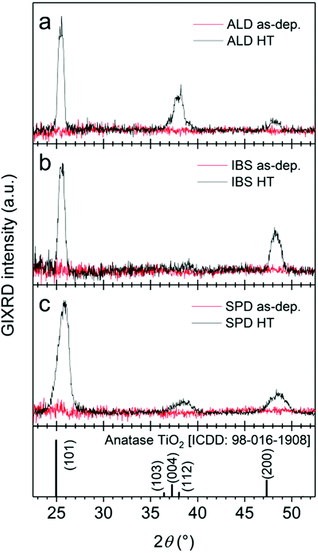 | ||
| Fig. 3 GIXRD of ALD, IBS and SPD as-deposited and heat-treated samples. | ||
The deviation of peak intensity ratios from powder diffractograms (ICDD card number 98-016-1908 for anatase TiO2) is an indication of crystal orientation anisotropy, i.e. texture.25 Furthermore, XRD peaks were observed at higher angles compared to the powder diffractograms. This can be caused by stress in TiO2 thin films which may have resulted from the rapid crystallization upon the heat-treatment. A strong (004) texture has been reported for Nd doped26 and N doped27 anatase TiO2 thin films where dopants have introduced strain in the lattice. For such an unrelaxed TiO2, the (001) plane has the lowest surface energy, whereas for relaxed TiO2 the (101) plane is the most favorable surface.28 Therefore, the reduction of the (004) XRD peak intensity and the high (101) to (004) peak intensity ratio suggests that the IBS TiO2 HT has a strong (101) plane texture.
A straightforward conclusion from GIXRD measurements is that for all three film deposition techniques the as-deposited TiO2 films are amorphous, though the exact stoichiometry of the films can be different. The heat treatment finally converts all three samples to anatase type of TiO2 films with different textures (different orientation of planes).
3.4 Transient absorption spectroscopy
Photo-carrier relaxation dynamics was studied by the pump–probe transient absorption (TA) spectroscopy method in transmittance and reflectance modes. The samples were excited at 320 nm and monitored in two wavelength ranges, 410–740 nm and 840–1050 nm. The results of measurements of the ALD HT sample are shown in Fig. 4 as an example. Apparently, the sample transmittance increases after photo-excitation in the visible range, at λ < 700 nm. However, the HT TiO2 does not absorb in the visible part of the spectrum and thus cannot become more transparent. The only feasible explanation for this observation is that the photo-excitation reduces the sample refractive index, and this results in the reduced amount of the light reflected from the sample surface and the increased amount of transmitted light.29 This is interpreted by the measurement system as a decrease in the sample absorbance. In order to separate the contributions of absorption and refractive index changes to the measured TA responses, the measurements were repeated with the same sample in reflectance mode and the results are presented in Fig. 4b. The results of measurements of other samples can be found in Fig. S8–S12 (ESI†).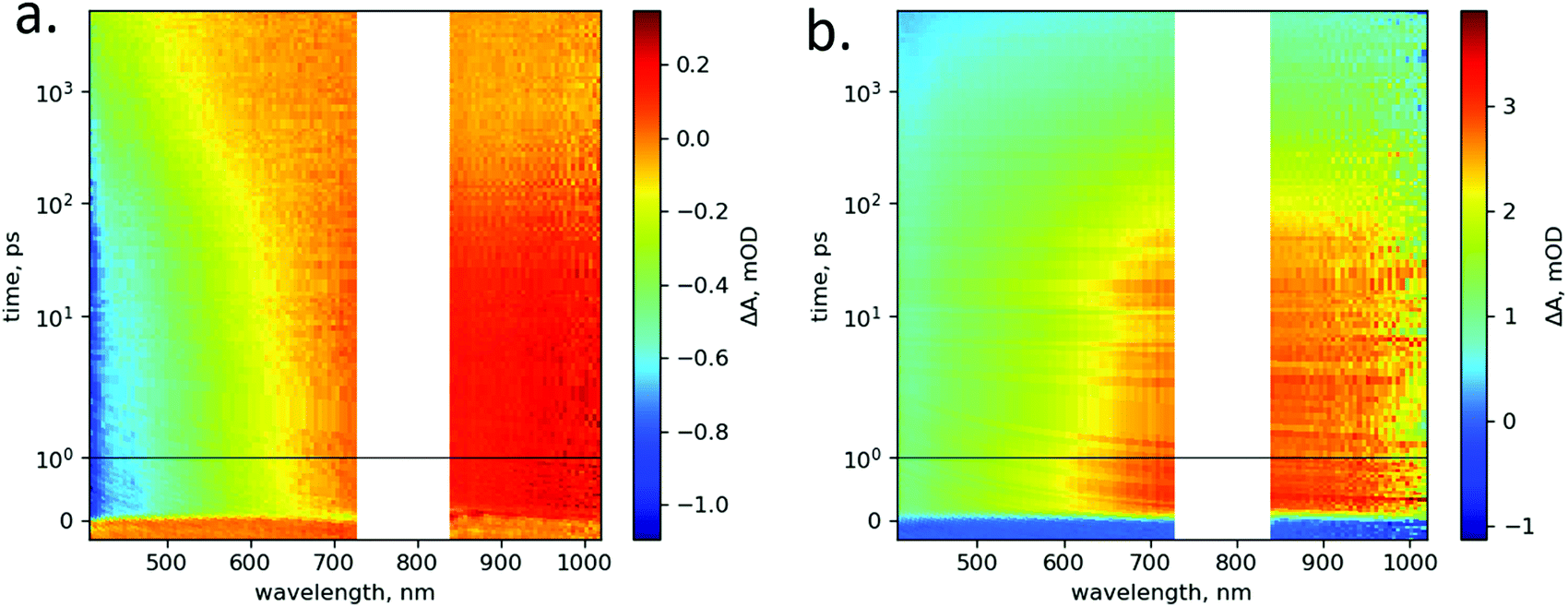 | ||
| Fig. 4 Transient absorption response of the ALD HT sample measured in (a) transmittance and (b) reflectance modes and presented as 2D maps. The time scale is linear till 1 ps delay time and logarithmic after that. The excitation wavelength is 320 nm. | ||
4 Data analysis and discussion
4.1 Absorbance and film thickness
The steady state spectra of the samples can be analysed to reveal the film thickness and porosity. The interference of the monitoring light reflected from the front and back film surface results in specific spectral features which depend on the film refractive index and thickness.30,31 These features are most pronounced when the film thickness is in the order of magnitude of the monitoring wavelength, but can be applied to thinner films, though with lower accuracy. The monitoring light propagation is calculated for the sample structure| air|photo − activelayer|substrate|air | (2) |
| n′ = (n − 1)p + 1 | (3) |
In order for the model to work well in the blue and near UV parts of the spectrum, one also needs to account for the sample absorption. This is especially important for the as-deposited sample when the crystal structures are not well formed and the film has detectable absorption due to a high degree of disorder and large number of defects and trap states. This is accounted for by adding a smoothed step-like absorption extinction coefficient switching from a constant value to zero at the wavelength corresponding to the band gap. The model is described in detail in the ESI† and was applied to fit the measured absorbance spectra of the sample. The blue side of the wavelength range was limited to 330 nm as the single-term Sellmeier refractive index model does not work well at shorter wavelengths. The result of the spectrum fit is presented in Fig. 5 using the examples of ALD as-deposited and HT samples. The fitting results for all samples are summarised in Table 2.
 | ||
| Fig. 5 Measured (Ameas) and modelled (Acalc) absorption spectra of ALD as-deposited and HT samples. The model uses an approximation for absorption extinction coefficient k, which is also shown for both samples, see text for details. | ||
| Sample | d (nm) | p | d × p (nm) |
|---|---|---|---|
| ALD as-deposited | 90.4 | 0.66 | 59.4 |
| ALD HT | 32.2 | 0.97 | 31.1 |
| IBS as-deposited | 23.1 | 1.05 | 24.3 |
| IBS HT | 31.9 | 0.91 | 28.9 |
| SPD as-deposited | 94.6 | 0.58 | 55.2 |
| SPD HT | 64.7 | 0.68 | 44.3 |
The spectra fit the result in p ≈ 1 for HT ALD and IBS samples. The calculated thickness d ≈ 30 nm is in good agreement with the thickness estimated by other methods. This confirms the formation of continuous and homogeneous TiO2 films in both cases. Also, the spectrum of the as-deposited IBS film is well approximated by the model and gives parameters close to expected (and of the HT sample). However, the thickness calculated for the as-deposited ALD sample, 90.4 nm, deviates significantly from the expectation, 30 nm. An apparent explanation is that the as-deposited film is porous, and this agrees with p = 0.66. The effective thickness can be estimated as d × p (the thickness without pores) and it is still almost two times larger than expected. The most possible reason for the discrepancy is the incorrect model for the refractive index spectrum of the as-deposited ALD films. Indeed, we used TiO2 polyxtal32 as a guess, but we lack actual knowledge of the refractive index.
The values of d and p are definitely the least accurate, as the absorption spectra model presumes uniform film thickness on the lateral scale. This assumption is particularly inaccurate for SPD samples as can be seen from the large scale AFM image presented in Fig. S2 (ESI†). Since the surface thickness is quite inhomogenous, the effective thickness (d × p) of the HT sample is 44.3 nm, which is close to the desired value of 30 nm and agrees with somewhat high absorption of SPD samples (Fig. 1a). This indicates that SPD films retain some porosity even after the heat treatment.
4.2 Transient absorbance spectra calculations
While measuring the TA spectrum of the sample, the probe light reflection takes place from both sides of the TiO2 film resulting in light interference inside the film, which makes exact calculations of the sample transmittance and reflectance rather complicated.22 However, if interference can be neglected due to the small sample thickness and/or small reflection at the film-substrate interfaces, eqn (1) can be used to calculate the absorbance from transmittance, T, and reflectance, R, spectra of the sample. Within this approximation the photoinduced transient absorbance, ΔA, can be calculated from the measured TA responses in transmittance mode, ΔAT, reflectance mode, ΔAR, and the steady state reflectance spectrum, R, of the sample as (for details see the ESI;† transient absorption (TA) measurements in transmittance and reflectance modes – estimation of the photoinduced absorbance change)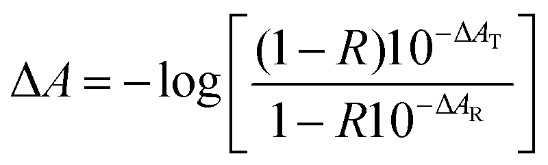 | (4) |
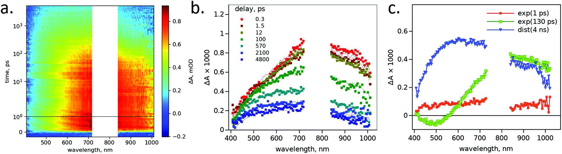 | ||
| Fig. 6 (a) Calculated ΔA response of the ALD HT sample, (b) time resolved ΔA spectra at different delay times, and (c) decay associated component spectra obtained from these data using the fit model consisting of two exponential (1 and 130 ps) and one distributed decay component (4 ns, see the text for details). | ||
By ignoring the fast (<1 ps) and relatively weak TA signals at the beginning, the absorbance change of all HT samples follows the same pattern: (1) the initially formed state has a broad-band absorption with a flat maximum in the range of 600–900 nm, which can be seen as the time resolved TA spectrum at 12 ps delay in Fig. 6b; (2) this is followed by the blue-shift of the absorption maximum to the 500–700 nm region with the time constant in the range of 50–130 ps (see Table 2), which can be seen at a longer delay time, e.g. at 2100 ps in Fig. 6b, and this is the spectrum of the long-lived distributed decay component.
The transient absorbance of the as-deposited samples is also broad-band and decays non-exponentially, but there is no visible change in the spectrum shape during the decay and from the very beginning (right after excitation) the broad absorption maximum is located in the visible part of the spectrum, 600–700 nm.
A comparison of the photo-carrier recombination dynamics in different samples is presented in Fig. 7 by plotting ΔA time profiles close to the maximum of the long-lived component. The decay plots for the HT samples are taken at 600 nm for comparison and are fitted by exponential and distributed decay time constants. Apparently, the difference in the lifetimes of the HT samples is rather minor, evidencing similar charge carrier dynamics. We note that the IBS HT sample depicts a bit more shallow decay profile compared to the other samples evidenced by the slightly higher transient absorbance signal for >1000 ps. Also, the lifetime dependence on the thickness of the samples was also studied. A 200 nm thick sample of TiO2 was prepared by IBS to study the dependence of the charge carrier lifetimes on the sample thickness. It was observed that with the increased thickness of films, the lifetime does not get any better, at least in the nanometer scale range, as shown in Table S2 (ESI†).
 | ||
| Fig. 7 Normalized ΔA decays in the visible part of the spectrum of the (a) as-deposited ALD, IBS and SPD samples at 670 nm and (b) HT samples at 600 nm. | ||
The decay profiles of the HT samples are rather similar to those reported by Durrant and co-authors for TiO2 anatase nanoparticles.34 They concluded that the nanostructure size has a minor effect on the photo-carrier recombination, and the main relaxation pathway is the bulk recombination. This agrees with our observation showing rather similar relaxation for three types of the samples after HT, which have rather different morphologies and different lateral sizes of the crystal domains.
The transient absorbance (ΔA) decay profiles of the as-deposited samples were almost identical at different wavelengths for the same sample but different for different samples. The latter is illustrated in Fig. 7a by presenting decays at 670 nm.
There are a number of theoretical, computational and experimental studies on the intra-band gap states in TiO2 and its spectral features.35–37 The broad absorbance band with maximum in the 700–900 nm range was assigned to trapped electrons and the band with maximum in the 450–650 nm range to trapped holes.35 The free electrons in the conduction band are expected to have slowly increasing absorption toward the longer wavelengths and show no spectral feature in the range of our study (410–1060 nm). There was also an analysis of hole trap states in the bulk and surface states,38 which predicts the absorption maximum of the bulk hole traps to be in the 600–700 nm range and surface traps at <550 nm. Based on these studies, we can suggest that the absorption observed in a few ps delay time (such as at 12 ps shown in Fig. 6b) is a mixture of absorption spectra of trapped electrons and holes, and shallow trapped electrons, which should have a broad and featureless TA spectrum. Trapping/detrapping of shallow trapped electrons is a slow process and it takes tens of picoseconds (130 ps in the case of the ALD HT sample) to establish an equilibrium of deep trapped electrons and holes. The recombination of the trapped carrier is slow, extended to the nanosecond time domain and most probably it is governed by the thermally activated carriers whose population must be very low in the wide band gap semiconductor such as TiO2.
This interpretation suggests that there are virtually no free electrons in the conduction band already at picosecond delay time, or the trapping process is fast, <1 ps. This agrees with the recent report of subpicosecond trapping of the photo-generated electrons.39 However, there must be a significant population of the shallow trapped electrons contributing to the carrier dynamics in the tens of picosecond time scale. However, experimentally, this is observed as a minor increase of the TA in the range of 400–500 nm indicated by a 130 ps component in the case of the ALD HT sample.
The as-deposited samples can be classified as amorphous TiO2. Although the as-deposited thin films prepared by ALD, IBS and SPD methods have apparently different amorphous nature and the carrier lifetime differs by more than one order in magnitude. The AFM images suggest very different morphologies of the samples prepared by these three methods. It should be noted that different metal–organic Ti precursor compounds and deposition temperatures were used for preparing ALD and SPD samples, whereas IBS used a physical vapor deposition technique without organic precursors that may reside in the thin films.
The ALD deposition temperature was 150 °C while the substrate temperature was 200 °C for SPD samples, which may result in different types of amorphous TiO2 as-deposited samples. However, at a qualitative level, the TA spectra of all as-deposited samples show broad bands with the maximum in the range of 600–750 nm, or in the same range as the long-lived components of the HT samples shown in Fig. 8. This can be attributed to trapped holes as explained in the case of the ALD HT sample in Fig. 6b. However, the absorption of the SPD HT sample is somewhat lower at the blue side of the band (<550 nm) which can be due to the different proportions of the bulk and surface trap states.
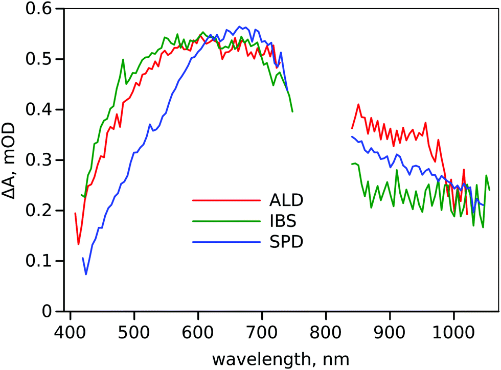 | ||
| Fig. 8 Decay associated spectra of the long-lived components of the HT samples deposited using ALD, IBS and SPD techniques. | ||
4.3 Evaluation of photocatalytic performance
To evaluate the photocatalytic activity of TiO2 thin films, the photodegradation test of methylene blue (MB) was conducted on all the as-dep. and HT thin films deposited via ALD, IBS and SPD techniques. MB degradation on a surface is commonly considered to follow the Langmuir–Hinshelwood mechanism in the first order, c = c0![[thin space (1/6-em)]](https://www.rsc.org/images/entities/char_2009.gif) exp(−kt), for which the rate constant, k, can be analyzed as the slope of −ln(c/c0) vs. time curve.40
exp(−kt), for which the rate constant, k, can be analyzed as the slope of −ln(c/c0) vs. time curve.40
A bare substrate was measured as a control sample (Fig. 9a) to show the magnitude of MB degradation without TiO2 thin films, for example, due to the MB photolysis. Fig. 9 shows that all the TiO2 thin films were photocatalytically active compared to the bare substrate which showed a negligible degradation rate of 0.0002 min−1. The degradation performance of all HT thin films improved as compared to that of the as-dep. samples. Also, it was interesting to find that the IBS HT films showed the highest degradation activity with a rate constant of 0.0042 min−1 (corresponds to the initial photonic efficiency of 0.0022%) as shown in Fig. 9b. This result is in compliance with our GIXRD and TAS measured data where the IBS HT samples showed the strongest texture and long lifetime of charge carriers. Also, the IBS HT thin films were composed of pure sputtered TiO2 as compared to HT thin films prepared by ALD and SPD techniques which are chemical vapor deposition processes and may contain some impurities from precursor materials. The catalytic activity of anatase TiO2 depends on the surface facet orientation. High reactivity facets (001) and (100)/(010) are desired for photocatalytic applications, but have also high surface energies and are therefore more rare.41,42 However, it should be noted that all the HT samples used for this study are of anatase phase and this phase of TiO2 is preferred over the rutile phase of TiO2, since it shows better photocatalytic activity as studied by Wang et al.43 The high-degree of oxide-defects in the as-deposited films resulted in short carrier lifetimes, and therefore, low photocatalytic activity. Also, a strong film texture is particular to physical vapor deposition techniques, such as IBS, and the adjustment of deposition parameters allows for further optimization of texture mediated TiO2 photocatalytic activity.44
 | ||
| Fig. 9 Photocatalytic degradation of MB under UV irradiation: (a) MB concentration change measured live during UV irradiation and (b) rate constants analyzed as the slope of −ln(c/c0) vs. time curves. The dashed lines are the linear fits to the data. | ||
4.4 Energy diagram
The band gaps for all the as-deposited and heat-treated samples prepared by ALD, IBS and SPD techniques are listed in Table 3. Assuming the absorption band position of trapped holes to be in the range of 500–700 nm, the energy level of the traps must be in the range of 1.8–2.5 eV over the VB, which agrees with previous experimental and theoretical studies.35,36 However, in our case this is most probably due to the superposition of the TA bands arising from the hole trap states and the electron trap states.| Samples | τ 1, ps | τ d, ps (δ) |
|---|---|---|
| ALD as-dep. | — | 0.9 (25) |
| ALD HT | 130 | 3600 (13) |
| IBS as-dep. | 3.3 | 170 (100) |
| IBS HT | 53 | 3600 (100) |
| SPD as-dep. | 1.6 | 50 (32) |
| SPD HT | 98 | 1400 (42) |
The estimation of the energy levels of shallow and deep electron traps is more complicated as there is no delay time at which absorption of trapped electrons could be observed. Therefore, we turn our attention to the hundred picosecond component. As discussed above, its most probable origin is the decay of the shallow trapped electron states. The characteristic feature of this component is a broad absorption band extended to the near IR range. The band shows absorption from 800–1100 nm but this is differential absorption, meaning that the process associated with it results in lower absorption at wavelengths >600 nm and somewhat higher absorption at shorter wavelengths. This agrees with the interpretation that the electrons at shallow traps can be (thermally) detrapped, and after some traveling, they can again be trapped by deep electron traps. A rough estimation puts electron traps in the range of 1.1–1.5 eV below the CB. It is interesting to note that the relative intensity of the hundred ps component is different for the HT samples prepared by different methods, but the shape is reasonably the same. Also our monitoring range was limited to 1100 nm at the long wavelength side, and most probably the band is extended further to the IR range. It was suggested that the electron trap states start at energies 0.1 eV below the CB.17 Considering all these, the energy diagram is presented in Fig. 10.
 | ||
| Fig. 10 Tentative energy ranges of the hole (h-traps) and electron (e-traps) traps in the band gap area. | ||
The fast sub-picosecond trapping of the CB carriers generated by photoexcitation was reported39 and our results are consistent with this observation. One reason for the fast trapping can be rather the high energy of these intra band gap states close to the bottom of the CB. This is observed as the TA band stretched to the IR part of the spectrum.
The TA response of the as-deposited samples is simpler in that there is no change in the spectrum shape and the TA has a non-pronounced band maximum in the 600–700 nm range. Although this band is closer to the expected TA spectrum of trapped holes, most probably there is a mixture of different structural disorders, and oxide defects specific to each deposition method. As a result, the TA spectra and lifetimes of the as-deposited samples are different. Nevertheless, the HT at 500 °C converts all three types of structures to poly-crystalline anatase films with almost similar carrier lifetimes (≈4 ns).
5 Conclusions
Three TiO2 deposition methods, ALD, IBS, and SPD, were used to prepare films with a nominal thickness of 30 nm. The as-deposited films prepared by all three methods were amorphous in nature. The photogenerated charge carrier lifetimes were different but shorter than 100 ps for all the as-deposited samples. Heat-treatment at 500 °C converted all the amorphous thin films to poly-crystalline anatase TiO2, albeit with different textures. Also, the AFM study of these samples showed that the morphology and grain size distribution of the films remained dependent on the deposition method. The ALD and IBS techniques resulted in most uniform films, and the SPD technique produced rather inhomogeneous films with their thickness changing in the range of 10–50 nm. Photo-carrier relaxation dynamics was studied using transient absorption (TA) spectroscopy. However, the TA response was affected by both absorption and refractive index changes. The thin film approximation (film thickness is much smaller than the probe wavelength) was used to calculate the TA from pump–probe measurements carried out in transmittance and reflectance modes. The study shows that despite the morphological differences, the carrier lifetimes of the heat-treated samples were virtually independent of the deposition method and extended to a nanosecond time domain (approx. 4 ns). From this point of view, the aim of this study, to hunt for preparing poly-crystalline thin films optimal for photocatalytic activities with longer lifetimes, was achieved in all three cases. As the lifetime of these thin films is independent of the deposition method, all of the above methods can be used for preparing TiO2 thin film photoelectrodes for photonic applications where a long carrier lifetime is desired and structural homogeneity is not critical. However, in TiO2 photocatalytic applications, higher activity can be obtained with strongly textured IBS TiO2 thin films.Conflicts of interest
There are no conflicts of interest to declare.Acknowledgements
Ramsha Khan acknowledges the Doctoral program of Tampere University for financial support. We thank Jesse Saari for providing TiO2 thin films prepared by ALD, Jarno Reuna for providing TiO2 thin films prepared by IBS, and Maning Liu and Paola Vivo for providing TiO2 thin films prepared by SPD for the project. This work is part of the Academy of Finland Flagship Programme, Photonics Research and Innovation (PREIN), Decision No. 320165. This work was supported by the Academy of Finland (decision No. 326461).References
- Z. Yu, H. Liu, M. Zhu, Y. Li and W. Li, Small, 2019, 1903378 Search PubMed.
- T. Moehl, J. Suh, L. Sévery, R. Wick-Joliat and S. D. Tilley, ACS Appl. Mater. Interface, 2017, 9, 43614–43622 CrossRef CAS PubMed.
- M. Khalil, E. S. Anggraeni, T. A. Ivandini and E. Budianto, Appl. Surf. Sci., 2019, 487, 1376–1384 CrossRef CAS.
- M. L. de Souza and P. Corio, Appl. Catal., B, 2013, 136–137, 325–333 CrossRef CAS.
- R. Khan, A. Riaz, M. Rabeel, S. Javed, R. Jan and M. A. Akram, Appl. Nanosci., 2019, 9, 1915–1924 CrossRef CAS.
- T.-P. Ruoko, K. Kaunisto, M. Bärtsch, J. Pohjola, A. Hiltunen, M. Niederberger, N. V. Tkachenko and H. Lemmetyinen, J. Phys. Chem. Lett., 2015, 6, 2859–2864 CrossRef CAS PubMed.
- Z. Tong, T. Peng, W. Sun, S. Liu, W. Guo and X.-Z. Zhao, J. Phys. Chem. C, 2014, 118, 16892–16895 CrossRef CAS.
- A. Khataee and M. Kasiri, J. Mol. Catal. A: Chem., 2010, 328, 8–26 CrossRef CAS.
- J. Schneider, M. Matsuoka, M. Takeuchi, J. Zhang, Y. Horiuchi, M. Anpo and D. W. Bahnemann, Chem. Rev., 2014, 114, 9919–9986 CrossRef CAS PubMed.
- M. Janczarek and E. Kowalska, Catalysts, 2017, 7, 317–333 CrossRef.
- M. R. Hoffmann, S. T. Martin, W. Choi and D. W. Bahnemann, Chem. Rev., 1995, 95, 69–96 CrossRef CAS.
- T. L. Thompson and J. T. Yates, Chem. Rev., 2006, 106, 4428–4453 CrossRef CAS PubMed.
- R. Qian, H. Zong, J. Schneider, G. Zhou, T. Zhao, Y. Li, J. Yang, D. W. Bahnemann and J. H. Pan, Catal. Today, 2019, 335, 78–90 CrossRef CAS.
- A. L. Linsebigler, G. Lu and J. T. Yates, Chem. Rev., 1995, 95, 735–758 CrossRef CAS.
- M. Kong, Y. Li, X. Chen, T. Tian, P. Fang, F. Zheng and X. Zhao, J. Am. Chem. Soc., 2011, 133, 16414–16417 CrossRef CAS PubMed.
- E. Wang, W. Yang and Y. Cao, J. Phys. Chem. C, 2009, 113, 20912–20917 CrossRef CAS.
- A. Yamakata and J. J. M. Vequizo, J. Photochem. Photobiol., C, 2019, 40, 234–243 CrossRef CAS.
- A. Yamakata, H. Vequizo, J. Jhon and M. Matsunaga, J. Phys. Chem. C, 2015, 119, 24538–24545 CrossRef CAS.
- S. Hu, M. R. Shaner, J. A. Beardslee, M. Lichterman, B. S. Brunschwig and N. S. Lewis, Science, 2014, 344, 1005–1009 CrossRef CAS PubMed.
- R. Khan, H. Ali-Löytty, J. Saari, M. Valden, A. Tukiainen, K. Lahtonen and N. V. Tkachenko, Nanomaterials, 2020, 10, 1567 CrossRef CAS PubMed.
- Y. Tachibana, K. Umekita, Y. Otsuka and S. Kuwabata, J. Phys. D: Appl. Phys., 2008, 41, 102002 CrossRef.
- H. P. Pasanen, P. Vivo, L. Canil, A. Abate and N. Tkachenko, Phys. Chem. Chem. Phys., 2019, 21, 14663–14670 RSC.
- H. Ali-Löytty, M. Hannula, J. Saari, L. Palmolahti, B. D. Bhuskute, R. Ulkuniemi, T. Nyyssönen, K. Lahtonen and M. Valden, ACS Appl. Mater. Interfaces, 2019, 11, 2758–2762 CrossRef PubMed.
- K. Usha, B. Mondal, D. Sengupta, P. Das, K. Mukherjee and Kumbhakar, Opt. Mater., 2014, 36, 1070–1075 CrossRef CAS.
- P. Acevedo-Peña, F. González, G. González and I. González, Phys. Chem. Chem. Phys., 2014, 16, 26213–26220 RSC.
- A. Ali, E. Yassitepe, I. Ruzybayev, S. Ismat Shah and A. S. Bhatti, J. Appl. Phys., 2012, 112, 113505 CrossRef.
- S. Deng, S. W. Verbruggen, S. Lenaerts, J. A. Martens, S. Van den Berghe, K. Devloo-Casier, W. Devulder, J. Dendooven, D. Deduytsche and C. Detavernier, J. Vac. Sci. Technol., A, 2014, 32, 01A123 CrossRef.
- A. Vittadini, A. Selloni, F. P. Rotzinger and M. Grätzel, Phys. Rev. Lett., 1998, 81, 2954–2957 CrossRef CAS.
- Y. M. Evtushenko, S. Romashkin, N. Trofimov and T. Chekhlova, Phys. Procedia, 2015, 73, 100–107 CrossRef CAS.
- A. Barybin and V. Shapovalov, Int. J. Opt., 2010, 137572 Search PubMed.
- T.-S. Oh, Y. S. Tokpanov, Y. Hao, J. W. C. and S. M. Haile, J. Appl. Phys., 2012, 112, 103535 CrossRef.
- R. D. Shannon, R. C. Shannon, O. Medenbach and R. X. Fischer, J. Phys. Chem. Ref. Data, 2002, 31, 931–970 CrossRef CAS.
- H. A. Santos, Porous Silicon Biomed. Appl., 2014, pp. 507–526 Search PubMed.
- M. Sachs, E. Pastor, A. Kafizas and J. R. Durrant, J. Phys. Chem. Lett., 2016, 7, 3742–3746 CrossRef CAS PubMed.
- F. Nunzi, F. De Angelis and A. Selloni, J. Phys. Chem. Lett., 2016, 7, 3597–3602 CrossRef CAS PubMed.
- T. Yoshihara, R. Katoh, A. Furube, Y. Tamaki, M. Murai, K. Hara, S. Murata, H. Arakawa and M. Tachiya, J. Phys. Chem. B, 2004, 108, 3817–3823 CrossRef CAS.
- R. Katoh, M. Murai and A. Furube, Chem. Phys. Lett., 2010, 500, 309–312 CrossRef CAS.
- P. Zawadzki, J. Phys. Chem. C, 2013, 117, 8647–8651 CrossRef CAS.
- Y. Zhang, D. T. Payne, C. L. Pang, C. Cacho, R. T. Chapman, E. Springate, H. H. Fielding and T. Geoff, J. Phys. Chem. Lett., 2019, 10, 5265–5270 CrossRef CAS PubMed.
- A. Houas, H. Lachheb, M. Ksibi, E. Elaloui, C. Guillard and J.-M. Herrmann, Appl. Catal., B, 2001, 31, 145–157 CrossRef CAS.
- H. G. Yang, C. H. Sun, S. Z. Qiao, J. Zou, G. Liu, S. C. Smith, H. M. Cheng and G. Q. Lu, Nature, 2008, 453, 638–641 CrossRef CAS PubMed.
- N. Roy, Y. Sohn and D. Pradhan, ACS Nano, 2013, 7, 2532–2540 CrossRef CAS.
- X. Wang, A. Kafizas, X. Li, S. J. A. Moniz, P. J. T. Reardon, J. Tang, I. P. Parkin and J. R. Durrant, JPCC, 2015, 119, 10439–10447 CAS.
- O. Lyandres, D. Finkelstein-Shapiro, P. Chakthranont, M. Graham and K. A. Gray, Chem. Mater., 2012, 24, 3355–3362 CrossRef CAS.
Footnote |
| † Electronic supplementary information (ESI) available: The modelling for steady state absorbance spectra, estimation of photoinduced absorbance change by transient absorption measurements, their interpretations and the distributed decay model for lifetime calculation of thin films. See DOI: 10.1039/d1cp02716f |
| This journal is © the Owner Societies 2021 |