
Gate-tunable superconductivity and charge-density wave in monolayer 1T′-MoTe2 and 1T′-WTe2†
Jun-Ho
Lee‡
 and
Young-Woo
Son
*
and
Young-Woo
Son
*
Korea Institute for Advanced Study, 85 Hoegiro, Seoul 02455, Korea. E-mail: hand@kias.re.kr; junholee@berkeley.edu
First published on 21st July 2021
Abstract
Using first-principles calculation methods, we reveal a series of phase transitions as a function of gating or electron doping in monolayered quantum spin Hall (QSH) insulators, 1T′-MoTe2 and 1T′-WTe2. With increasing electron doping, we show that a phonon mediated superconducting phase is realized first and is followed by a charge density wave (CDW) phase with a nonsymmorphic lattice symmetry. The newly found CDW phase exhibits Weyl energy bands with spin–orbit coupling with fractional band filling, and reforms into a topological nontrivial phase with fully filled bands. The robust resurgence of the QSH state coexisting with the CDW phase is shown to originate from band inversions induced by the nonsymmorphic lattice distortion through the strong electron–phonon interaction, thus suggesting the realization of various interfacial states between superconducting states, and various CDW and topological states on a two-dimensional crystal by inhomogeneous gating or doping.
1 Introduction
Layered transition metal dichalcogenides (TMDs) have shown collective phenomena alongside topological electronic properties. Prominent examples are charge density wave (CDW),1 superconducting (SC) phases,2 the two-dimensional (2D) quantum spin Hall (QSH) state,3 and three-dimensional (3D) Weyl semimetal (WSM) state,4 to name a few. Among these, CDW and SC in bulk TMDs have been studied over several decades.1,2 Recently, there have been intensive efforts to understand the new physical properties shown in a single-layer limit of TMDs that may differ from those in their bulk form.5–12Maintaining their stoichiometry, TMDs have several polymorphic structures showing radically different electronic properties.13 The most common atomic structures are the trigonal prismatic (2H) and octahedral (1T) form. For single-layer MoTe2 and WTe2, the 1T structure is unstable and turns into the distorted octahedral structure called the 1T′ form.3,14 For many other TMDs, the 1T′ structure has not been observed as it is a metastable structure. Recently, novel synthetic approaches have been developed and 1T′ structures for other TMDs have also been realized.12 One of the most fascinating phenomena shown in the 1T′ structure is the emergence of topologically nontrivial states. For example, the 2D QSH state in a single-layer 1T′ structure is theoretically predicted3 and was experimentally confirmed recently.15–19
The aforementioned distinct states could be enhanced, intertwined, or made to coexist by external perturbations such as chemical or carrier doping.20–25 Doping- or edge-induced phase transitions between different polymorphic structures for 2H and 1T forms have been studied theoretically26–29 and experimentally,30,31 while those for single-layer 1T′ structures have not been studied well. As the 1T′-TMDs have shown various topological states differing from 2H and 1T forms, there is interesting interplay between carrier doping, structural phase transition, collective phenomena and topological states. Recently, there have been theoretical studies on doping-induced superconductivity in monolayer 1T′-WTe2![[thin space (1/6-em)]](https://www.rsc.org/images/entities/char_2009.gif) 32,33 assuming inversion symmetry. Although a pristine 1T′-WTe2 preserves the inversion symmetry, experiments on superconductivity9–11 were performed using the gating that breaks the inversion symmetry, lifting degeneracy in electronic structure and phonon dispersion. As the proposed mechanisms for the superconductivity assumed inversion symmetry, the lifting degeneracy may lead to a different mechanism for the superconductivity such as Ising pairing.34 Thus, it should be revisited considering the effect of gating. Motivated by rapid developments in this field realizing extremely thin samples,15–18,31 we have performed a comprehensive theoretical study on possible phase transitions as a function of external gating in single-layer 1T′-MoTe2 and 1T′-WTe2.
32,33 assuming inversion symmetry. Although a pristine 1T′-WTe2 preserves the inversion symmetry, experiments on superconductivity9–11 were performed using the gating that breaks the inversion symmetry, lifting degeneracy in electronic structure and phonon dispersion. As the proposed mechanisms for the superconductivity assumed inversion symmetry, the lifting degeneracy may lead to a different mechanism for the superconductivity such as Ising pairing.34 Thus, it should be revisited considering the effect of gating. Motivated by rapid developments in this field realizing extremely thin samples,15–18,31 we have performed a comprehensive theoretical study on possible phase transitions as a function of external gating in single-layer 1T′-MoTe2 and 1T′-WTe2.
In this work, using various first-principles calculation methods, we explore a series of phase transitions in single-layer 1T′-MoTe2 and 1T′-WTe2 (henceforth MoTe2 and WTe2 for simplicity), with a field-effect transistor (FET) gating setup.35 We find that the phase transitions in the 1T′-TMDs differ from those shown in other TMDs. Without doping, single-layer 1T′ TMDs are QSH insulators.3 We show that with low doping, a phonon-mediated SC phase with a maximum transition temperature (Tc) of 9 K could be realized. With increasing doping, we find that the SC phase fades away and that a new CDW phase emerges. The crystal structures in the newly found CDW phase are distorted in such a way as to respect the nonsymmorphic lattice symmetry, which leads to 2D Weyl semimetallic energy bands with spin–orbit coupling.36 We also find that a topological QSH state appears again when the energy bands of the new CDW phase are fully filled. So, the coexistence of the QSH state and CDW phase are predicted. As the doping concentrations considered in this study have already been achieved in recent experiments,22,23,25 we believe that various interesting interfacial structures between the SC phase, CDW states and topological insulator properties,37–40 can be manipulated on single-layer 1T′-TMDs by external doping or gating.
2 Computational methods
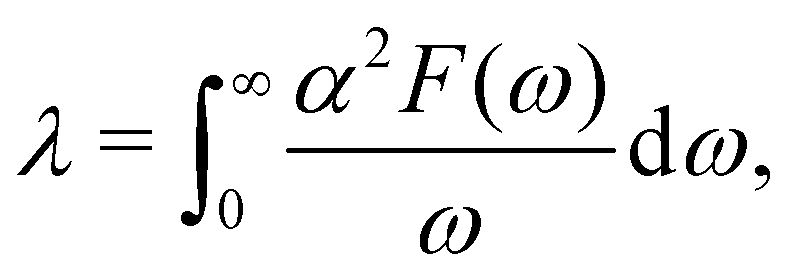
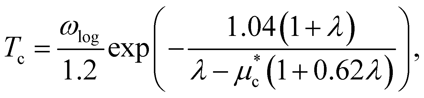
We performed density-functional theory calculations using a quantum espresso package.41,42 We used the PBE generalized gradient approximation43 for the exchange–correlation functional with scalar and fully relativistic optimized norm-conserving pseudopotentials from the PseudoDojo library.44 We used 80 Ry planewave energy cutoff. We simulated the electron and hole doping by realistic modeling of the FET gating geometry as shown in Fig. 1a.35 The dipole for the dipole correction is placed at zdip = ddip/2 with ddip = 0.02L, with L being the unit-cell size in the direction perpendicular to the 2D plane. The charged plane modeling the gate electrode was placed close to the dipole at zmono = 0.021L. A potential barrier with a height of V0 = 2.5 Ry and a width of db = 0.1L was used. We used the epw package to compute the Eliashberg equation and electron–phonon coupling (EPC) with fine grids.45,46 The k-point integration was done with 10 × 20 × 1 (5 × 4 × 1 and 5 × 10 × 1) Monkhorst–Pack scheme for a 1 × 1 (2 × 5 and 2 × 2) cell of 1T′ phase. Structural relaxation was performed until the Hellmann–Feynman forces on all the atoms and total energy change became less than 10−4 a.u. and 10−6 a.u. simultaneously. The vacuum region between adjacent slabs is ∼15 Å. The Methfessel–Paxton scheme for smearing is used with 0.02 Ry of Gaussian spreading. We used the density-functional perturbation theory (DFPT) to calculate the phonon-dispersion relation with 4 × 8 × 1 q-point grids with a threshold for self-consistency of 10−18 Ryd. The electronic wave functions required for the Wannier interpolation within epw are calculated on uniform and Γ-centered 4 × 8 × 1 k-point grids. For the initial guess of Wannierization, 22 Wannier functions, five d-orbitals for two Mo (W) atoms and three p-orbitals for four Te atoms, are used to describe the electronic structure. In order to solve the Eliashberg equations, we evaluated electron energies, phonon frequencies, and electron–phonon matrix elements on fine grids using the methods in ref. 47. The fine grids contain 20 × 40 × 1 k and q-points. The frequency cutoff (ωc) is set to 1 eV. The Eliashberg spectral function considered here reads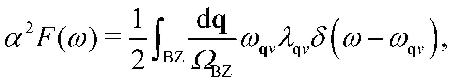 | (1) |
 | (2) |
 | (3) |
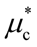 is the Coulomb pseudopotential with 0.16. We neglect the effect of the spin–orbit coupling (SOC) in computing EPC.
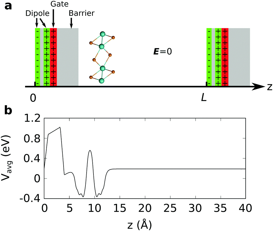 | ||
| Fig. 1 (a) Schematic figure of the field effect transistor gating with the atomic structure of the 1T′-transition metal dichalcogenide (TMD). The atomic structure is viewed along the chalcogen chain direction. The length of the unit cell along z is given by L. (b) Plane-averaged potential profile where we used the vacuum region of ∼27 Å. The sharp peak of Vavg around ∼8 Å corresponds to the position of the transition metals of TMD. The barrier between the fictitious gate and TMD is in between the vacuum and TMD. | ||
3 Results
First, we computed the equilibrium lattice parameters of MoTe2 (WTe2) as a = 6.380 (6.331) Å and b = 3.457 (3.495) Å, which are consistent with previous theoretical studies.3,32 Then, we calculated electronic band structures with and without SOC as shown in Fig. 2(c) and (d), confirming that the inclusion of SOC suppresses a crossing point and provides the nontrivial topological Z2 invariant, a hallmark of the QSH state. Fermi surfaces (FSs) are composed of a hole pocket centered at the Γ point and electron pockets located on the ΓY line. We projected the FSs onto Mo (W) 4d (5d) and Te 5p orbitals using FermiSurfer.48 For MoTe2, the electron (hole) pockets can be characterized by the Mo 4d (Te 5p), while for WTe2 the W 5d and Te 5p are more hybridized in the electron and the hole pockets because of the different configuration of the valences of Mo and W in the vicinity of FS.49 For both cases the orbital distributions are highly anisotropic.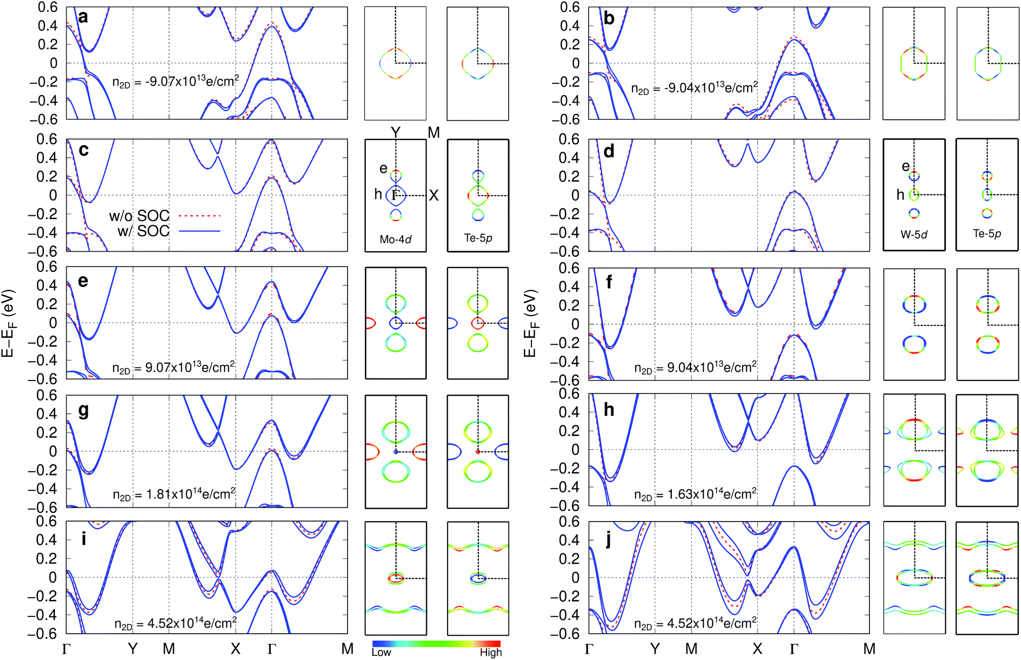 | ||
| Fig. 2 Band structure and Fermi surface (FS) of monolayer (c) 1T′-MoTe2 and (d) 1T′-WTe2. The blue solid (red-dashed) line is calculated with (without) spin–orbit coupling. The middle and right panels are Mo(W) d and Te p orbitals projected Fermi surfaces, respectively. (e), (g), and (i) are band structures and FSs of MoTe2 are calculated by several n2D. (f), (h), and (i) are band structures and FSs of WTe2 are calculated by several n2D. (a) and (b) are electronic structures with the hole doping for MoTe2 and WTe2, respectively. | ||
On top of that, we applied the FET gating using the methods described in the previous section. The doping concentration (n2D) can be defined as n2D = x/A in electrons per cm2, where x is the amount of electrons added to the unit cell and A is the area of the unit cell. Fig. 2(a), (b) and (e)–(j) represent band structures and FSs for several n2D. Fermi energy (EF) shifts up (down) by electron (hole) doping and the bandwidth and the relative energies between bands slightly changes as well. For the bands with SOC the degeneracy of the energy bands is lifted due to inversion symmetry breaking in the FET gating. This can be seen in the 2D plane-averaged potential profile along the z-axis where the potential profile is asymmetric with respect to TMD as shown in Fig. 1(b). The spin splitting increases with increasing n2D and is highly momentum dependent. For WTe2 the splitting is more significant than that of MoTe2 because of the more substantial SOC effect. The corresponding FS also changes a lot. For the case of hole doping, the electron pocket at Γ point disappears and the size of the hole pocket increases for both MoTe2 and WTe2. The size of the hole pocket at Γ point decreases with electron doping and eventually disappears. For MoTe2, the area of electron pocket located on the ΓY line increases with doping and a new electron pocket featuring the strong d-character emerges at the X point. For WTe2, similar behavior is shown while an electron pocket with p-character develops on the XM line earlier than the electron pocket with d-character at the X point. In higher n2D (∼4.52 × 10¹⁴ e cm−2), for both cases, quasi-1D-like bands parallel to the kx-axis with hole pockets at the Γ point can be obtained, being similar to the result obtained by high coverage hydrogen adsorption.50 We note that recent ARPES experiments on MoTe2 on a bilayer graphene shows similar FSs with doping.17
Fig. 3(a)–(i) represent phonon dispersions, phonon density of states (PHDOS), and Eliashberg spectral function (α2F(ω)) of MoTe2 and WTe2 with varying n2D. The most noticeable change upon electron doping is that at  XM and
  Y the low energy acoustic phonons were softened significantly. While the homogeneous background charge does not break inversion symmetry,32 the FET gating lifts the degeneracy of phonon modes in the M–Y line. We also computed phonon frequencies of MoTe2 in the vicinity of
  XM with a fine q-grid at n2D= 1.80 × 10¹⁴ e cm−2 and confirmed that
  XM has lower frequency than
  XM as shown in Fig. S1 (ESI†). The computed phonon frequency at
  XM is found to be −45.16 cm−1, while it is found to be −42.10 cm−1 at
  XM. We also compared energy gain by the CDW formation with 2 × 5 and 2 × 8 phases which correspond to the
  XM and
  XM, and found that the 2 × 5 CDW is more stable than the 2 × 8 CDW by ∼10 meV per 1 × 1 unitcell in a wide range of n2D (see Fig. S2, ESI†). The PHDOS around 50 cm−1 is slightly increased and subsequently α2F(ω) is strongly enhanced, implying that the low energy acoustic phonon modes are responsible for the SC phase of doped MoTe2 and WTe2.
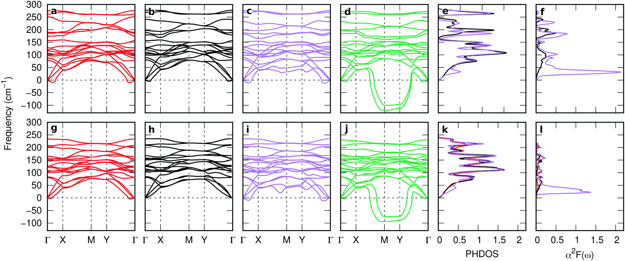 | ||
| Fig. 3 Phonon dispersion of MoTe2 for (a) n2D = −9.07 × 10¹³ e cm−2 (hole doping), (b) pristine, (c) n2D = 1.36 × 10¹⁴ e cm−2, and (d) n2D = 3.63 × 10¹⁴ e cm−2. (e) Phonon density of states and (f) α2F(ω) for pristine and n2D = 1.36 × 10¹⁴ e cm−2. Phonon dispersion of WTe2 with (g) n2D = −9.04 × 10¹³ e cm−2, (h) pristine, (i) n2D = 9.04 × 10¹³ e cm−2, and (j) n2D = 4.06 × 10¹⁴ e cm−2. (k) Phonon density of states and (f) α2F(ω) for pristine and n2D = 9.04 × 10¹³ e cm−2. | ||
The calculated Tc of the SC phase using the Allen-Dynes formula, electron–phonon coupling constant (λ), and logarithmic average of phonon frequencies (ωlog) as a function of n2D are plotted in Fig. 4. For pristine MoTe2 (WTe2) the calculated λ and Tc are 0.59 (0.33) and 1.039 (0.004) K, respectively. As n2D increases, λ increases and ωlog decreases, showing the dome-shaped T–n diagram. The computed maximum Tc of MoTe2 (WTe2) reaches 9.16 (6.30) K at n2D = 1.36 × 10¹⁴ (9.04 × 10¹³) e cm−2. It is reported that Tc of a pristine 1T′-MoTe2 is 7.6 K,11 and that for WTe2 the Tc ∼ 1 K at n2D ∼ 1.8 × 10¹³ e cm−1.10,29 Our calculation results agree with the experiments qualitatively.9–11 The over/underestimation of Tc can be found in doped MoS221 and other materials too, due to limitations of the current theoretical approximations.51,52 Although the observed maximum Tc in WTe2 is ∼1 K for the available n2D in the experiment, we anticipate that Tc could be enhanced if n2D could be increased. For a hole doped region (n2D < 0), there is no significant phonon softening and the calculated λ and Tc tend to be weakened, which is consistent with the experimental.10 Based on our results, the SC in the gated single-layer MoTe2 and WTe2 can be attributed to the electron doping-induced softening of the low energy acoustic phonon.8–11 It is noteworthy that the softened acoustic phonon-induced SC is likely to be a universal mechanism for superconductivity in 2D TMDs.21,53,54
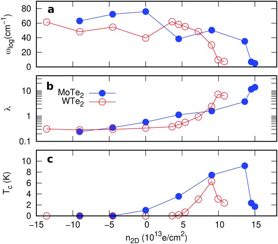 | ||
| Fig. 4 (a) Logarithmic average of phonon frequencies (ωlog), (b) electron–phonon coupling constant (λ), and (c) superconducting transition temperature (Tc) for MoTe2 (filled blue circles) and WTe2 (open red circles) in a wide range of n2D. | ||
With further doping, the atomic structures of the both 1T′-MoTe2 and 1T′-WTe2 become unstable. When n2D ≥ 1.40(1.03) × 1014 e cm−2 for MoTe2 (WTe2), the frequencies of the softened acoustic phonon mode become negative around qCDW, 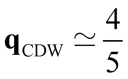 XM. The lattice instability is relieved by forming a new stable structure in a 2 × 5 supercell with respect to the unit cell (called as 2 × 5 CDW hereafter) where the transition metals (TMs) along with zigzag chain direction (y) are distorted, as shown in Fig. 5(a). We plot the displacement of TMs along the y-direction (dy) for several n2D in Fig. 5(b). Although the patterns of dy in MoTe2 and WTe2 differ a little, they together show the 2 × 5 CDW phase from the phonon instability at the same qCDW. There are weak lattice distortions in the vicinity of Mo4 and Mo6 of MoTe2, while in WTe2 the distortions are more significant. These distinctions could be ascribed to the difference in mass and the valence configuration of Mo and W atoms.49 The largest dy of TMs in MoTe2 (WTe2) is ∼6.4(4.6)% of the 1 × 1 lattice constant, implying the origin of the 2 × 5 CDW would be strong electron–phonon coupling rather than Fermi surface nesting.5,55,56 It is noticeable that the lattice distortion in the 2 × 5 CDW phase respects a nonsymmorphic crystal symmetry as will be discussed later. For much higher n2D ∼ 2.72(1.99) × 1014 e cm−2 for MoTe2 (WTe2) qCDW changes from
  XM to M as shown in Fig. 3(d) and (j). The M point is commensurate with a 2 × 2 supercell and we calculate 2 × 2 CDW phases in the same way as applied to the 2 × 5 CDW, as shown in Fig. 5(c) and (d).
 | ||
| Fig. 5 Optimized positions of transition metals (TMs) in (a) 2 × 5 and (c) 2 × 2 CDW phases of WTe2. Blue open circles represent TMs without lattice displacements. Pink dashed and gray solid lines in (a) represent the 1T′ unitcell and a glide mirror line (Mŷ), respectively. Brown dashed lines in (c) represent a primitive cell of the 2 × 2 CDW. The displacements of TMs along the y axis for (b) the 2 × 5 and (d) the 2 × 2 CDW of MoTe2 (left) and WTe2 (right) are shown. Blue (gray) solid lines stand for the left (right) chain of TMs in (a) and (c). (e) Calculated CDW formation energies for MoTe2 (left) and WTe2 (right) as a function of n2D. Black open (blue filled) circles represent the 2 × 2(2 × 5) CDW. | ||
We investigated the stability of the 2 × 5 and the 2 × 2 CDW phases by calculating their formation energy as a function of n2D. Here we will consider a range, 9.04 × 10¹³ e cm−2 ≤ n2D ≤ 4.53 × 10¹⁴ e cm−2. The formation energy of I × j CDW states can be written as
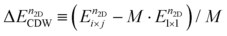 | (4) |
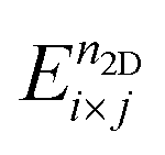 stands for the total energy of an i × j CDW phase, and
 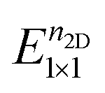 stands for the total energy of the 1 × 1 1T′ unitcell for a given doping of n2D and M ≡ i × j. Fig. 5(e) displays the
  for MoTe2 and WTe2. The transition to the 2 × 5 CDW in WTe2 takes place at lower n2D than MoTe2. For a given n2D, the
 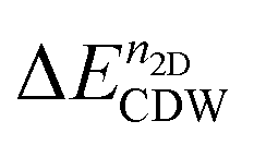 of WTe2 is larger than that of MoTe2, implying the enhanced stability and a higher CDW transition temperature of WTe2 than that of MoTe2. When n2D ≥ 2.90(1.90) × 1014 e cm−2 for MoTe2 (WTe2), the
  of the 2 × 2 CDW is more stable than that of the 2 × 5 CDW. The change of the relative stability between the two CDW phases coincides with the change of the instability qCDW from
  XM to M. The n2D region that can find the 2 × 5 CDW of WTe2 is narrow compared to that of MoTe2.
The new CDW phase of doped 1T′-TMDs shows interesting topological electronic properties owing to their crystal symmetries. Fig. 6(a) and (b) represent the electronic band structures of the 2 × 5 CDW of MoTe2 for n2D = 2.27 × 10¹⁴ e cm−2 and WTe2 for n2D = 1.63 × 10¹⁴ e cm−2, respectively. The calculated  at these n2D for MoTe2 and WTe2 are −13.11 meV and −7.71 meV, respectively. The crystal structure of the 2 × 5 CDW possesses nonsymmorphic symmetry that can be written as
 | (5) |
 is a half-translation along the x-axis. The nonsymmorphic symmetry without the inversion symmetry guarantees that the energy bands must have twofold-degenerated Weyl points along Mŷ invariant lines at ky = 0 and π, even in the presence of the SOC as shown in Fig. 6(a) and (b).36 Thanks to the FET condition considered here that allows us to make fractional band filling, we can place the Weyl points in the vicinity of the shifted EF by gating. From the calculated band structures, we can infer that 1T′-MoTe2 and WTe2 are quite unique materials showing the 2D Weyl in its doped single-layer and the 3D Weyl fermions in its stacked structure.4
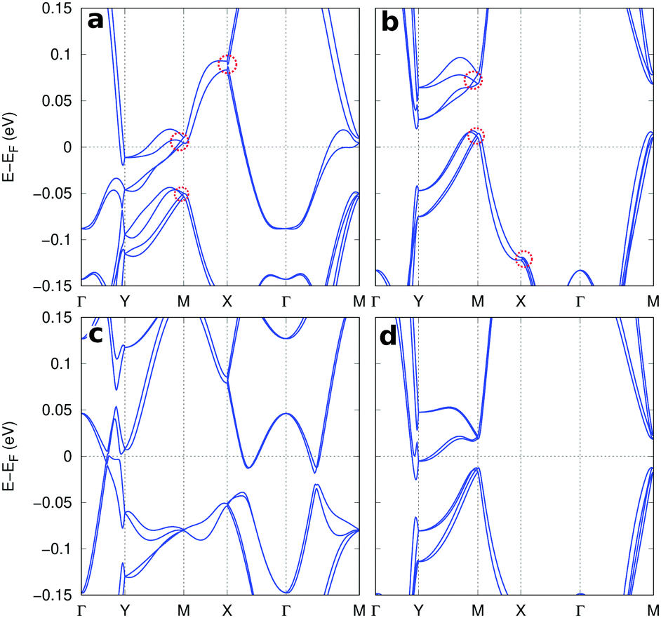 | ||
| Fig. 6 Electronic band structures of 2 × 5 CDW phase with SOC at (a) n2D = 2.27 × 10¹⁴ e cm−2 in MoTe2, (b) n2D = 1.63 × 10¹⁴ e cm−2 in WTe2, (c) x = 4e/2 × 5 × 1 in MoTe2, and (d) x= 4e/2 × 5 × 1 in WTe2. Red dashed circles in (a) and (b) represent symmetry-protected twofold degenerated Weyl points. | ||
The new 2 × 5 CDW phase coexists with the QSH state as the CDW energy bands are fully filled. We plotted the Mo d and Te p projected band structures of 2 × 5 CDW of MoTe2 with n2D of 1.81 × 10¹⁴ e cm−2 that corresponds to four electrons in the 2 × 5 × 1 supercell as shown in Fig. S3 (ESI†). We found that S1 and S2 bands at the Γ point [Fig. S3(a), ESI†] feature inverted band characters around EF, similar to the pristine 1T′ WTe2.3 Here, no crossing points exist in the entire Brillouin zone because of the lack of inversion symmetry. As we include the SOC, the inverted bands develop Rashba splitting and form new hybridized bands as shown in Fig. 6(c) and (d), respectively. The calculated  at this n2D for MoTe2 and WTe2 are −5.71 meV and −11.16 meV, respectively. Although the computed band structures show semimetallic character, we expect that the 2 × 5 CDW band structure can have a finite spectral gap between inverted bands when the environmental screening changes,57 or when gentle external mechanical perturbations are applied. Following some experiments demonstrating substrate-induced tensile strain along the y axis,3,16,17 we applied similar tensile strains along the same direction and computed band structures as shown in Fig. S4. We confirm that a band gap forms while preserving inverted band character (Fig. S4(a)–(c), ESI†). As we increase the strain more than 2%, the inverted band character disappears.
4 Conclusions
We theoretically demonstrate a series of phase transitions between the QSH state, SC phase, and CDW phase in gated monolayer 1T′-TMDs as a function of doped charges induced by the planar gate in a field effect transistor device set up, or equivalently homogeneous ionic gating. The newly found CDW states in partially filled MoTe2 and WTe2 are shown to coexist with a 2D Weyl semimetallic state thanks to nonsymmorphic crystal symmetry of the distorted CDW lattices. Furthermore, with fully filled bands, they re-entered the QSH insulating phase, coexisting with the CDW states. Considering various intriguing interfacial states realized between topological states and the superconducting phase such as Majorana fermions,37–40 we believe that doping controlled electronic phase transitions in monolayer 1T′-TMDs shown here, could provide a new facile platform toward topological state engineering.Conflicts of interest
There are no conflicts to declare.Acknowledgements
We thank Sejoong Kim, Seoung-Hun Kang, Heejun Yang, Bohm-Jung Yang, and Thomas Brumme for fruitful discussions. Y.-W. S. was supported by the National Research Foundation (NRF) grant funded by the Korean government (MSIP) (Grant No. 2017R1A5A1014862, SRC program: vdWMRC center). The computing resources were supported by the Center for Advanced Computation (CAC) of KIAS.Notes and references
- J. A. Wilson, F. J. Di Salvo and S. Mahajan, Adv. Phys., 2001, 50, 1171–1248 CrossRef.
- J. Wilson and A. Yoffe, Adv. Phys., 1969, 18, 193–335 CrossRef CAS.
- X. Qian, J. Liu, L. Fu and J. Li, Science, 2014, 346, 1344–1347 CrossRef CAS.
- A. A. Soluyanov, D. Gresch, Z. Wang, Q. Wu, M. Troyer, X. Dai and B. A. Bernevig, Nature, 2015, 527, 495–498 CrossRef CAS PubMed.
- M. Calandra, I. I. Mazin and F. Mauri, Phys. Rev. B: Condens. Matter Mater. Phys., 2009, 80, 241108 CrossRef.
- X. Xi, L. Zhao, Z. Wang, H. Berger, L. Forró, J. Shan and K. F. Mak, Nat. Nanotechnol., 2015, 10, 765–769 CrossRef CAS PubMed.
- M. M. Ugeda, A. J. Bradley, Y. Zhang, S. Onishi, Y. Chen, W. Ruan, C. Ojeda-Aristizabal, H. Ryu, M. T. Edmonds, H.-Z. Tsai, A. Riss, S.-K. Mo, D. Lee, A. Zettl, Z. Hussain, Z.-X. Shen and M. F. Crommie, Nat. Phys., 2016, 12, 92 Search PubMed.
- Y. Saito, T. Nojima and Y. Iwasa, Nat. Rev. Mater., 2017, 2, 16094 Search PubMed.
- V. Fatemi, S. Wu, Y. Cao, L. Bretheau, Q. D. Gibson, K. Watanabe, T. Taniguchi, R. J. Cava and P. Jarillo-Herrero, Science, 2018, 362, 926 CrossRef CAS.
- E. Sajadi, T. Palomaki, Z. Fei, W. Zhao, P. Bement, C. Olsen, S. Luescher, X. Xu, J. A. Folk and D. H. Cobden, Science, 2018, 362, 922 CrossRef CAS PubMed.
- D. A. Rhodes, A. Jindal, N. F. Q. Yuan, Y. Jung, A. Antony, H. Wang, B. Kim, Y.-C. Chiu, T. Taniguchi, K. Watanabe, K. Barmak, L. Balicas, C. R. Dean, X. Qian, L. Fu, A. N. Pasupathy and J. Hone, Nano Lett., 2021, 21, 2505 CrossRef CAS.
- Z. Lai, Q. He, T. H. Tran, D. V. M. Repaka, D.-D. Zhou, Y. Sun, S. Xi, Y. Li, A. Chaturvedi, C. Tan, B. Chen, G.-H. Nam, B. Li, C. Ling, W. Zhai, Z. Shi, D. Hu, V. Sharma, Z. Hu, Y. Chen, Z. Zhang, Y. Yu, X. Renshaw Wang, R. V. Ramanujan, Y. Ma, K. Hippalgaonkar and H. Zhang, Nat. Mater., 2021, 20, 1113 CrossRef CAS PubMed.
- M. Chhowalla, H. S. Shin, G. Eda, L.-J. Li, K. P. Loh and H. Zhang, Nat. Chem., 2013, 5, 263 CrossRef PubMed.
- D. H. Keum, S. Cho, J. H. Kim, D.-H. Choe, H.-J. Sung, M. Kan, H. Kang, J.-Y. Hwang, S. W. Kim, H. Yang, K. J. Chang and Y. H. Lee, Nat. Phys., 2015, 11, 482 Search PubMed.
- Z. Fei, T. Palomaki, S. Wu, W. Zhao, X. Cai, B. Sun, P. Nguyen, J. Finney, X. Xu and D. H. Cobden, Nat. Phys., 2017, 13, 677 Search PubMed.
- S. Tang, C. Zhang, D. Wong, Z. Pedramrazi, H.-Z. Tsai, C. Jia, B. Moritz, M. Claassen, H. Ryu, S. Kahn, J. Jiang, H. Yan, M. Hashimoto, D. Lu, R. G. Moore, C.-C. Hwang, C. Hwang, Z. Hussain, Y. Chen, M. M. Ugeda, Z. Liu, X. Xie, T. P. Devereaux, M. F. Crommie, S.-K. Mo and Z.-X. Shen, Nat. Phys., 2017, 13, 683 Search PubMed.
- S. Tang, C. Zhang, C. Jia, H. Ryu, C. Hwang, M. Hashimoto, D. Lu, Z. Liu, T. P. Devereaux, Z.-X. Shen and S.-K. Mo, APL Mater., 2018, 6, 026601 Search PubMed.
- S. Wu, V. Fatemi, Q. D. Gibson, K. Watanabe, T. Taniguchi, R. J. Cava and P. Jarillo-Herrero, Science, 2018, 359, 76–79 CrossRef CAS PubMed.
- H. W. Kim, S.-H. Kang, H.-J. Kim, K. Chae, S. Cho, W. Ko, S. Jeon, S. H. Kang, H. Yang, S. W. Kim, S. Park, S. Hwang, Y.-K. Kwon and Y.-W. Son, Nano Lett., 2020, 20, 5837–5843 CrossRef CAS PubMed.
- E. Morosan, H. W. Zandbergen, B. S. Dennis, J. W. G. Bos, Y. Onose, T. Klimczuk, A. P. Ramirez, N. P. Ong and R. J. Cava, Nat. Phys., 2006, 2, 544 Search PubMed.
- M. Rösner, S. Haas and T. O. Wehling, Phys. Rev. B: Condens. Matter Mater. Phys., 2014, 90, 245105 CrossRef.
- Y. Yu, F. Yang, X. F. Lu, Y. J. Yan, Y.-H. Cho, L. Ma, X. Niu, S. Kim, Y.-W. Son, D. Feng, S. Li, S.-W. Cheong, X. H. Chen and Y. Zhang, Nat. Nanotechnol., 2015, 10, 270 CrossRef CAS PubMed.
- J. T. Ye, Y. J. Zhang, R. Akashi, M. S. Bahramy, R. Arita and Y. Iwasa, Science, 2012, 338, 1193–1196 CrossRef CAS PubMed.
- Y. Ge and A. Y. Liu, Phys. Rev. B: Condens. Matter Mater. Phys., 2013, 87, 241408 CrossRef.
- L. J. Li, E. C. T. O'Farrell, K. P. Loh, G. Eda, B. Özyilmaz and A. H. Castro Neto, Nature, 2016, 529, 185 CrossRef CAS.
- M. Kan, J. Y. Wang, X. W. Li, S. H. Zhang, Y. W. Li, Y. Kawazoe, Q. Sun and P. Jena, J. Phys. Chem. C, 2014, 118, 1515–1522 CrossRef CAS.
- Y. Li, K.-A. N. Duerloo, K. Wauson and E. J. Reed, Nat. Commun., 2016, 7, 10671 CrossRef CAS.
- W. Zan, Z. Hu, Z. Zhang and B. I. Yakobson, Nanoscale, 2016, 8, 19154 RSC.
- W. Zan, Z. Zhang, Y. Yang, X. Yao, S. Li and B. I. Yakobson, Nanotechnology, 2019, 30, 075701 CrossRef PubMed.
- Y.-C. Lin, D. O. Dumcenco, Y.-S. Huang and K. Suenaga, Nat. Nanotechnol., 2014, 9, 391 CrossRef CAS PubMed.
- Y. Wang, J. Xiao, H. Zhu, Y. Li, Y. Alsaid, K. Y. Fong, Y. Zhou, S. Wang, W. Shi, Y. Wang, A. Zettl, E. J. Reed and X. Zhang, Nature, 2017, 550, 487 CrossRef CAS PubMed.
- W. Yang, C. J. Mo, S. B. Fu, Y. Yang, F. W. Zheng, X. H. Wang, Y. A. Liu, N. Hao and P. Zhang, Phys. Rev. Lett., 2020, 125, 237006 CrossRef CAS.
- Y. M. Xie, B. T. Zhou and K. T. Law, Phys. Rev. Lett., 2020, 125, 107001 CrossRef CAS PubMed.
- X. Xi, Z. Wang, W. Zhao, J. H. Park, K. T. Law, H. Berger, L. Forró, J. Shan and K. F. Mak, Nat. Phys., 2016, 12, 139 Search PubMed.
- T. Brumme, M. Calandra and F. Mauri, Phys. Rev. B: Condens. Matter Mater. Phys., 2014, 89, 245406 CrossRef.
- S. M. Young and C. L. Kane, Phys. Rev. Lett., 2015, 115, 126803 CrossRef PubMed.
- L. Fu and C. L. Kane, Phys. Rev. Lett., 2008, 100, 096407 CrossRef PubMed.
- L. Fu and C. L. Kane, Phys. Rev. B: Condens. Matter Mater. Phys., 2009, 79, 161408 CrossRef.
- S. Hart, H. Ren, T. Wagner, P. Leubner, M. Mühlbauer, C. Brüne, H. Buhmann, L. W. Molenkamp and A. Yacoby, Nat. Phys., 2014, 10, 638 Search PubMed.
- V. S. Pribiag, A. J. A. Beukman, F. Qu, M. C. Cassidy, C. Charpentier, W. Wegscheider and L. P. Kouwenhoven, Nat. Nanotechnol., 2015, 10, 593 CrossRef CAS PubMed.
- P. Giannozzi, S. Baroni, N. Bonini, M. Calandra, R. Car, C. Cavazzoni, D. Ceresoli, G. L. Chiarotti, M. Cococcioni, I. Dabo, A. Dal Corso, S. de Gironcoli, S. Fabris, G. Fratesi, R. Gebauer, U. Gerstmann, C. Gougoussis, A. Kokalj, M. Lazzeri, L. Martin-Samos, N. Marzari, F. Mauri, R. Mazzarello, S. Paolini, A. Pasquarello, L. Paulatto, C. Sbraccia, S. Scandolo, G. Sclauzero, A. P. Seitsonen, A. Smogunov, P. Umari and R. M. Wentzcovitch, J. Phys.: Condens. Matter, 2009, 21, 395502 CrossRef.
- P. Giannozzi, O. Andreussi, T. Brumme, O. Bunau, M. B. Nardelli, M. Calandra, R. Car, C. Cavazzoni, D. Ceresoli, M. Cococcioni, N. Colonna, I. Carnimeo, A. Dal Corso, S. de Gironcoli, P. Delugas, R. A. DiStasio Jr., A. Ferretti, A. Floris, G. Fratesi, G. Fugallo, R. Gebauer, U. Gerstmann, F. Giustino, T. Gorni, J. Jia, M. Kawamura, H.-Y. Ko, A. Kokalj, E. Küçükbenli, M. Lazzeri, M. Marsili, N. Marzari, F. Mauri, N. L. Nguyen, H.-V. Nguyen, A. O. de-la Roza, L. Paulatto, S. Poncé, D. Rocca, R. Sabatini, B. Santra, M. Schlipf, A. P. Seitsonen, A. Smogunov, I. Timrov, T. Thonhauser, P. Umari, N. Vast, X. Wu and S. Baroni, J. Phys.: Condens. Matter, 2017, 29, 465901 CrossRef CAS PubMed.
- J. P. Perdew, K. Burke and M. Ernzerhof, Phys. Rev. Lett., 1996, 77, 3865–3868 CrossRef CAS PubMed.
- D. R. Hamann, Phys. Rev. B: Condens. Matter Mater. Phys., 2013, 88, 085117 CrossRef.
- J. Noffsinger, F. Giustino, B. D. Malone, C. H. Park, S. G. Louie and M. L. Cohen, Comput. Phys. Commun., 2010, 181, 2140 CrossRef CAS.
- S. Poncé, E. R. Margine, C. Verdi and F. Giustino, Comput. Phys. Commun., 2016, 209, 116 CrossRef.
- F. Giustino, M. L. Cohen and S. G. Louie, Phys. Rev. B: Condens. Matter Mater. Phys., 2007, 76, 165108 CrossRef.
- M. Kawamura, Comput. Phys. Commun., 2019, 239, 197 CrossRef CAS.
- H.-J. Kim, S.-H. Kang, I. Hamada and Y.-W. Son, Phys. Rev. B, 2017, 95, 180101 CrossRef.
- J. Seok, J.-H. Lee, S. Cho, B. Ji, H. W. Kim, M. Kwon, D. Kim, Y.-M. Kim, S. H. Oh, S. W. Kim, Y. H. Lee, Y.-W. Son and H. Yang, 2D Mater., 2017, 4, 025061 CrossRef.
- Z. Li, G. Antonius, M. Wu, F. H. Da Jornada and S. G. Louie, Phys. Rev. Lett., 2019, 122, 186402 CrossRef CAS PubMed.
- Z. Li, M. Wu, Y.-H. Chan and S. G. Louie, Phys. Rev. Lett., 2021, 126, 146401 CrossRef CAS PubMed.
- C. Heil, S. Poncé, H. Lambert, M. Schlipf, E. R. Margine and F. Giustino, Phys. Rev. Lett., 2017, 119, 087003 CrossRef.
- J. Simonin, Phys. Rev. B: Condens. Matter Mater. Phys., 1986, 33, 7830 CrossRef.
- K. Rossnagel, J. Phys.: Condens. Matter, 2011, 23, 213001 CrossRef CAS PubMed.
- M. D. Johannes and I. I. Mazin, Phys. Rev. B: Condens. Matter Mater. Phys., 2008, 77, 165135 CrossRef.
- J. Ryou, Y.-S. Kim, S. Kc and K. Cho, Sci. Rep., 2016, 6, 29184 CrossRef CAS PubMed.
Footnotes |
| † Electronic supplementary information (ESI) available: Acoustic phonon dispersion of MoTe along XM line. Comparison of energetics of 2 × 5 and 2 × 8 CDW phases. Projected band structures of 2 × 5 CDW. Effect of tensile strain to the band structure of the 2 × 5 CDW. See DOI: 10.1039/d1cp02214h |
| ‡ Present address: Department of Physics, University of California, Berkeley, CA 94720, USA. |
| This journal is © the Owner Societies 2021 |