
 Open Access Article
 This Open Access Article is licensed under a Creative Commons Attribution-Non Commercial 3.0 Unported Licence
The energy level alignment of the ferrocene–EGaIn interface studied with photoelectron spectroscopy†
Nipun Kumar
Gupta‡
ab,
Thorsten
Schultz‡
 cd,
Senthil Kumar
Karuppannan
a,
Ayelet
Vilan
e,
Norbert
Koch
*cd and
Christian A.
Nijhuis
*abf
cd,
Senthil Kumar
Karuppannan
a,
Ayelet
Vilan
e,
Norbert
Koch
*cd and
Christian A.
Nijhuis
*abf
aDepartement of Chemistry, Faculty of Science, National University of Singapore, Singapore, Singapore
bCentre for Advanced 2D Materials, National University of Singapore, 6 Science Drive 2, Singapore 117546, Singapore
cInstitut für Physik, Humboldt-Universität zu Berlin, Newtonstraße 15, 12489 Berlin, Germany. E-mail: norbert.koch@physik.hu-berlin.de
dHelmholtz Zentrum Berlin für Materialien und Energie GmbH, Albert-Einstein Straße 15, 12489 Berlin, Germany
eDepartment of Chemical and Biological Physics, Weizmann Institute of Science, Rehovot 76100, Israel
fDepartment of Molecules and Materials, MESA+ Institute for Nanotechnology and Center for Brain-Inspired Nano Systems, Faculty of Science and Technology, University of Twente, P.O. Box 217, 7500 AE Enschede, The Netherlands. E-mail: c.a.nijhuis@utwente.nl
First published on 26th May 2021
Abstract
The energy level alignment after the formation of a molecular tunnel junction is often poorly understood because spectroscopy inside junctions is not possible, which hampers the rational design of functional molecular junctions and complicates the interpretation of the data generated by molecular junctions. In molecular junction platforms where the top electrode–molecule interaction is weak; one may argue that the energy level alignment can be deduced from measurements with the molecules supported by the bottom electrode (sometimes referred to as “half junctions”). This approach, however, still relies on a series of assumptions, which are challenging to address experimentally due to difficulties in studying the molecule–top electrode interaction. Herein, we describe top electrode–molecule junctions with a liquid metal alloy top electrode of EGaIn (which stands for eutectic alloy of Ga and In) interacting with well-characterised ferrocene (Fc) moieties. We deposited a ferrocene derivative on films of EGaIn, coated with its native GaOx layer, and studied the energy level alignment with photoelectron spectroscopy. Our results reveal that the electronic interaction between the Fc and GaOx/EGaIn is very weak, resembling physisorption. Therefore, investigations of “half junctions” for this system can provide valuable information regarding the energy level alignment of complete EGaIn junctions. Our results help to improve our understanding of the energy landscape in weakly coupled molecular junctions and aid to the rational design of molecular electronic devices.
Introduction
In molecular electronics, it is challenging to deduce the mechanism of charge transport across electrode–molecule–electrode junctions because changes in the energy levels of the molecules caused by the molecule–electrode interactions cannot be independently measured, complicating the interpretation of current density–voltage, J(V), data obtained from these junctions.1–5 For large area molecular junctions, which consist of self-assembled monolayers (SAMs) supported by the bottom electrode, it is common practice to characterise the SAM to obtain the energy level alignment of the bottom electrode–SAM structure with spectroscopy (usually in ultra-high vacuum, UHV) or electrochemistry (in electrolyte), for instance, which then serves as the starting point to discuss the electrical behaviour of metal–SAM–metal junctions.6–8 This analysis, however, assumes that the top-electrode interacts very weakly with the molecules so that the change in environment (e.g., replacing UHV or electrolyte with the top-electrode) can be neglected. This assumption certainly does not hold for chemisorbed top contacts (which involve charge transfer between the molecule and the electrode), or top contacts that are reactive (including top electrodes generated by break junction techniques), which consist of highly unsaturated (and therefore reactive) metal atoms,9,10 but it may hold for techniques that rely on physisorbed top-contacts, such as junctions based on top electrodes of graphene,11 spin-coated polymers,12 evaporated carbon,13 nanoparticles,14 or liquid metals (Hg)15 and the eutectic Ga–In alloy (EGaIn, 75% Ga and 25% In by weight),16,17 although charge reorganisation (induced by, for instance, electronic push back effects) between the molecule and the electrode may still be significant.6,18–20The top-electrode‖molecule interaction (Γ), where ‘‖’ represents a van der Waals contact, plays a major role in the junction characteristics and determines the tunnelling rates,21–23 affects the potential drops across the junctions,24,25 or changes the tunnelling barrier height (energy level alignment).5,26 Frisbie and co-workers investigated the changes in the energy level alignment of molecular junctions (with conducting probes as top-contacts) with transition voltage spectroscopy and were able to relate the properties of these junctions to those of the corresponding “half-junctions”, i.e., the electrode–SAM interface, studied with ultraviolet photoelectron spectroscopy (UPS).22,23,27 For instance, they found that the contact resistance of their molecular junctions decreased with increasing work function of the electrode (Φ, in eV; they studied junctions with Ag, Au, and Pt top/bottom electrodes and all combinations thereof) determined with UPS. They also reported a correlation between transition voltage of these junctions with the direct hole injection barrier height ΔE (ΔE = EHOMO − EF) determined with UPS, where EF is the Fermi level and EHOMO is the energy of the highest occupied molecular orbital (HOMO) level, both given with respect to the vacuum level (thus corresponding to Φ and the ionisation energy, respectively). These results imply that the energy level alignment of their system is predetermined by the bottom electrode–SAM contact (the top electrode SAM–contact appears to play a minor role in their system for unexplained reasons). In principle, however, the top-electrode can also cause changes in the energy level alignment for the same reasons as the bottom electrode.3,9,26,28 Besides the work function, other factors, such as chemical potential of the molecule, polarisability of the interface, or the type and strength of the molecule–electrode interaction, also affect ΔE and the HOMO–LUMO (LUMO = lowest unoccupied molecular orbital) gap significantly.6–8,29 These effects combined can result in large reductions of ΔE inside the junction (ΔEjunc) with respect to that of the electrode–molecule interface determined with UPS. For example, these reductions can be up to a factor of 25 in single molecule junctions which are often based on relatively strong chemisorbed electrode–molecule contacts.3,9,30–32 On the other hand, one could argue that for platforms with physisorbed molecule–electrode contacts, changes in the energy level alignment are mainly induced by the push back effect (Pauli exclusion principle). However, this can still lead to an appreciable decrease in Φ of commonly used metals by up to 1 eV.6,18–20 Physisorption of redox-active molecules can result in even larger Φ shifts by up to 1.6 eV due to (partial) charge transfer between the metal surface and the redox centre.33–35 Therefore, the presumption that in junctions with physisorbed top contacts, the top electrode only causes small changes in the energy level alignment is not per se reliable.
In molecular junctions, the shape of the J(V) curves can be analysed to estimate the energy level alignment of the junctions. For instance, in transition voltage spectroscopy, the J(V) curves are re-casted in Fowler–Nordheim plots after which often a dip in the plot is observed; this dip is then assumed to be the voltage at which a molecular orbital level enters the bias window.36 This analysis, however, relies on a series of assumptions, the most important one is that this dip reflects a change in the mechanism of charge transport from off- to on-resonant tunnelling (involving a molecular frontier orbital). Various studies have shown, however, that this is not always the case and that the dip can also be caused by other factors including defects, presence of a metal oxide,37 or asymmetry in the junctions,38,39 and it does not work for off-resonant tunnelling.38,40 Normalised differential conductance (NDC) analysis has been used to analyse the conductance traces, which has been widely used by the scanning tunnelling microscopy community to identify, for example, conductance peaks.41 Vilan42 has shown that this type analysis makes it possible to extract the scaling voltage (V0), which is closely related to the transition voltage (Vtrans) that is equivalent to ΔE (in eV).
The “EGaIn technique” is a versatile method to make metal–molecule–metal junctions, which has been utilised to study in the detail the mechanisms of charge transport and to demonstrate and study various phenomena, including dipole interactions in SAMs,43–46 thermoelectric effects,47,48 quantum interference,49 memory effects,25,39,50,51 or molecular-scale light–matter interactions.52 The EGaIn electrode is coated with an oxide layer that forms spontaneously in air and it is self-limiting to a thickness of 0.7 nm. It is yet highly conductive because it contains oxygen vacancies, and gives this material non-Newtonian properties.16 The oxide layer can be quite rough (depending on how the material is shaped) and may contain large oxide particles. Just below the oxide layer is a layer rich in In while deeper layers resemble the bulk composition of EGaIn.16,53,54 Due to its non-Newtonian behaviour, the contact between the EGaIn and the SAM is non-invasive. Since the EGaIn is passivated by a thin GaOx layer, it is chemically inert, does not damage the SAM, and prevents the bulk EGaIn form alloying with the bottom electrode.
In the past, we have studied in detail well-performing molecular diodes of the form of metal–S(CH2)11Fc‖GaOx/EGaIn (Fc = ferrocene).55–58 The mechanism of rectification involves a transition from off-resonant tunnelling at positive applied bias to resonant tunnelling at negative applied bias, involving the HOMO of the Fc moiety. This change in the mechanism of charge transport is readily visible in the current–voltage characteristics of these junctions, which help us to readily identify when the HOMO enters the bias window (in contrast to the rather featureless current–voltage characteristics generated by junctions with rather simple alkanethiols or conjugated molecules). The role of the C11 spacer is to decouple the Fc unit from the bottom electrode and to provide efficient molecular packing in the monolayers. The interpretation of the data generated by junctions prepared with the EGaIn technique usually assumes a weak SAM‖GaOx/EGaIn interaction, because the EGaIn-tip is prepared ex situ and covered with the passivating layer of GaOx. This assumption formed the basis for understanding and explaining EGaIn-based junctions, and especially in understanding the operating mechanism of the molecular diodes based on Fc;59–61 this assumption, however, has not been experimentally validated and it is not clear whether it holds given the defective nature of the GaOx layer. For instance, defects in oxide layers can induce tail states or gap states, potentially complicating the interpretation of molecular junctions with GaOx/EGaIn.19,62,63 Recently, we reported that the surface roughness associated with the cone-shaped tips of GaOx/EGaIn results in significant potential drops between the SAM and the top electrode.59
Herein, we report a detailed study on the electronic structure of the molecule‖GaOx/EGaIn interface with photoelectron spectroscopy (PES). Deposition of Fc–(CH2)14–Fc by sublimation on films of GaOx/EGaIn allowed us to study the molecule‖GaOx/EGaIn interface by analysing the EGaIn core levels, as well as the molecular HOMO level and its onset with respect to EF. Our results show that the interaction between the Fc moiety and GaOx/EGaIn is indeed very weak. To corroborate the PES results with the J(V) characteristics of an Ag–S(CH2)11Fc‖GaOx/EGaIn junction, we performed NDC analysis to extract at which voltage the HOMO level enters the bias window, and we find that the ΔE estimated from ex situ and in situ characterisation techniques are comparable. Our results help to understand the mechanism of charge transport in EGaIn junctions, and hopefully inspire others also to characterise molecule‖top electrode interactions in addition to, as is now common practice, molecule–bottom electrode interactions.
Experimental methods
Synthesis
Synthesis and characterisation of Fc–(CH2)14–Fc is reported in Section S1 (ESI†). Briefly, the precursor 1,14-tetradecandioic acid was reacted with oxalyl chloride to prepare 1,14-tetradecanoyldichloride, which was converted to 1,14-diferrocenoyl tetradecane via a Friedel–Crafts acylation with ferrocene. The carbonyl moieties in 1,14-diferrocenoyl tetradecane were reduced by Clemmenson reduction to give the final product, 1,14-diferrocenyl tetradecane (Fc–(CH2)14–Fc).GaOx/EGaIn film preparation
The preparation of the GaOx/EGaIn films is described in detail in Section S2 (ESI†). The GaOx/EGaIn films with a thickness of <0.1 mm were prepared on Si wafers and borosilicate glass substrates which were cut into 2 × 2 cm2 pieces and cleaned by sonication in piranha for 15 min followed by drying an oven at 80 °C for 3 hours after rinsing with de-ionised water. A drop of EGaIn was placed on the surface and distributed evenly on the substrate by pressing a glass test tube (Pyrex) on the EGaIn drop and then rolling it over the entire substrate. A freshly prepared polydimethylsiloxane stamp was utilised to strip off excess EGaIn by pressing the stamp firmly on the film followed by removal of the stamp similar to previously reported methods where continuous EGaIn films with thickness of a few micrometres can be achieved.64EGaIn film characterisation
The films were characterised with optical microscopy (LEICA DM 2500 M), scanning electron microscopy (JEOL JSM-6701F field emission scanning electron microscope).Deposition of Fc–(CH2)14–Fc on the GaOx/EGaIn films
After introduction of the GaOx/EGaIn films into ultra-high vacuum (<10−8 mbar), they were cooled down to −30 °C to freeze the GaOx/EGaIn. At this temperature, the samples were sputtered with an Argon ions at 5 × 10⁻⁵ mbar and an acceleration voltage of 2 kV for 15 min to remove adventitious contaminations.65 An oxide signal remained even after sputtering, as evidenced from the survey spectrum as explained in Section S4 (ESI†), which is in agreement with earlier investigations.16 Next, the samples were transferred under UHV to the deposition chamber kept at room temperature. The Fc–(CH2)14–Fc and the tetratetracontane (TTC) molecules were evaporated in UHV from quartz crucibles mounted on a W coil that was used to heat the crucibles resistively. The molecules were evaporated at a rate of 0.5–2 Å min−1, where the nominal thickness was measured with a quartz crystal microbalance, assuming a density of 1.38 g cm−3, as suggested by the manufacturer (Prevac) for organic molecules.Photoelectron spectroscopy (PES)
All PES measurements were performed using adjoined preparation and analysis chambers with base pressures of less than 10−8 mbar. X-Ray photoelectron spectroscopy (XPS) spectra were recorded using the radiation of a non-monochromated dual anode X-ray source DAR 400 from ScientaOmicron (hνAl = 1486.6 eV, hνMg = 1253.6 eV) and ultraviolet photoelectron spectroscopy (UPS) spectra were recorded using the radiation of a He discharge lamp HIS 13 from ScientaOmicron (hνHeI = 21.2 eV, hνHeII = 40.8 eV). Attenuation filters, which decreased the UV flux by a factor of 10, were used to minimise beam damage to the molecules. We performed the UPS measurements right after deposition, prior to the XPS measurements, as prolonged X-ray exposure can lead to degradation of the molecules (see Fig. S16, ESI†). The kinetic energy of the emitted electrons was detected by a Specs Phoibos 100 hemispherical analyser with a resolution of ≈150 meV. During the measurements of the secondary electron cut-off (SECO) a bias of −10 V was applied between the sample and the analyser. The binding energy scale was calibrated by measuring the Fermi-edge of a polycrystalline gold reference sample. We did not observe any charging effects, which indirectly confirms the high conductivity of the GaOx layer in agreement with earlier works.16,19,59,62,63,66,67J(V) measurements
The junction formation, collection and analysis of J(V) data was performed as previously reported with a home built EGaIn setup, and cone-shaped tips of EGaIn were utilised as the top electrode for the study.56 All Ag bottom electrodes were prepared following a previously reported template stripping method.57Results and discussion
EGaIn films and the junctions
Fig. 1 shows the Ag–S(CH2)11Fc‖GaOx/EGaIn molecular diode schematically, where ‘–’ represents a covalent contact, ‘/’ represents the contact between EGaIn and GaOx, and ‘‖’ indicates a physisorbed contact. As mentioned in the introduction, the energy level alignment of the M–S(CH2)n–Fc interface (with M = Au or Ag, n = 0–15) has been studied in detail before,55 but the S(CH2)nFc‖GaOx interface has not been characterised independently. Here we study the Fc‖GaOx/EGaIn interaction using films of GaOx/EGaIn with Fc functionalised molecules adsorbed on it, as schematically illustrated in Fig. 1B, with PES. Although Fc has been directly deposited on a variety of substrates including metals, Cu,68 Si,69 graphite,70 the layers of Fc on such substrates are only stable at cryogenic temperatures (<200 K) in UHV, because of weak interactions with such surfaces. Native Fc readily sublimes and, because of its anticipated weak interaction with GaOx/EGaIn, we prepared Fc–(CH2)14–Fc to facilitate our experiments. The use of Fc–(CH2)14–Fc has the advantage of having (i) two Fc units per molecule, which improves the detectability in a PES experiment, (ii) an alkyl chain spacer with a deep lying HOMO that is unlikely to interfere with the interpretation of the results, (iii) a moderate sublimation temperature of 413 K, and (iv) it forms stable films on metals under UHV conditions.71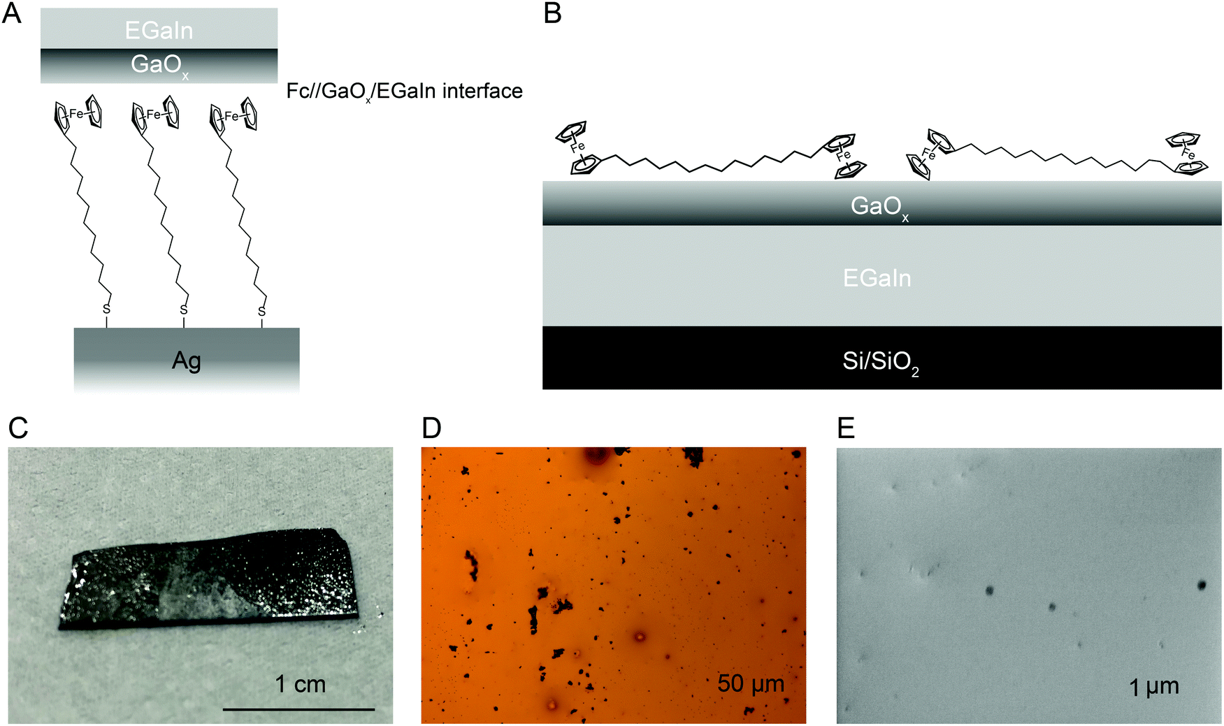 | ||
| Fig. 1 (A) Schematic illustration of the Ag–S(CH2)11Fc‖GaOx/EGaIn junction and (B) of the Fc–(CH2)14–Fc deposited on a layer of GaOx/EGaIn on a Si/SiO2 substrate. (C) A photograph, (D) an optical microscopy image, and (E) a scanning electron microscopy image, of the GaOx/EGaIn film. | ||
Fig. 1C shows a photograph of the GaOx/EGaIn film and Fig. 1D-E show an optical and SEM image, respectively, of the GaOx/EGaIn surface with different magnification. The images show that the EGaIn forms a film on the Si surface with small oxide lumps that can be seen as black spots; the presence of these relatively large gallium oxide particles has been reported before on the surface of drops of EGaIn.16 The texture and appearance of the GaOx/EGaIn films on Si wafers is comparable to GaOx/EGaIn films deposited on polymers by microcontact printing for applications in flexible electronics.64,72 Usually, these large oxide particles can be seen by eye in the bottle of EGaIn as received from the supplier, but they are not present on cone-shaped EGaIn tips73 likely because such tips are made using a small Hamilton syringes with an inner needle diameter of about 10 μm.
XPS of Fc–(CH2)14–Fc on GaOx/EGaIn films
We investigated the GaOx/EGaIn core levels before and after deposition of Fc–(CH2)14–Fc with XPS. We sequentially deposited layers of Fc–(CH2)14–Fc with nominal thicknesses of 0.5, 1.0, 2.0, and 5.0 nm by evaporation on the GaOx/EGaIn films cleaned by sputtering. Fig. 2 shows the (A) Ga 3d, (B) In 3d, (C) Ga 2p, (D) O 1s, (E) C 1s and (F) Fe 2p core level spectra of 0.5 nm and 5 nm thick films of Fc–(CH2)14–Fc. All other spectra are reported in Section S3 (ESI†). The sputter cleaned GaOx/EGaIn film does not show XPS signals for C 1s and N 1s, which suggests that adventitious contaminations were completely removed from surface of the GaOx/EGaIn film. We used the same peak assignments from published results,16,74 and we observed doublets with spin orbit splitting of 0.46 eV of Ga0 (∼18.8 eV), Ga1+ (∼19.0 eV), Ga3+ (∼20.5 eV), peaks of the In0 (∼16.3 eV) and In3+ (∼17.3 eV) species in the Ga 3d and In 3d spectra (Fig. 2A), doublets with spin orbit splitting of 7.6 eV of In0 (∼443.9 eV) and In3+ (∼445.2 eV) in the In 3d spectra (Fig. 2B), and Ga0 (∼1116.8 eV), Ga1+ (∼1117.8 eV) and Ga3+ (∼1118.8 eV) in the spectra Ga 2p3/2 spectra (Fig. 2C) with a spin orbit splitting of 26.9 eV. Two oxygen peaks are observed in Fig. 2D and correspond to oxide (∼531.5 eV)75 and the suboxide (∼532.7 eV) of In and Ga. The C 1s signal was observed at ∼285.4 eV76 (Fig. 2E) after deposition of 0.5 nm of Fc–(CH2)14–Fc. The relative contribution from C sp2 from the Fc units and C sp3 from the CH2 units could not be resolved with our setup. Also, the Fe 2p signal could not be resolved for the films with a nominal thickness of <2.0 nm, likely because of the combination of the low ratio of C![[thin space (1/6-em)]](https://www.rsc.org/images/entities/char_2009.gif) :Fe of 17:1 of Fc–(CH2)14–Fc, thinner than expected films, and limited reasonable acquisition times for the Fe 2p core level for the first two depositions. After deposition of Fc–(CH2)14–Fc with a nominal thickness of 2.0 nm, however, we observed the Fe 2p3/2 signal at ∼708.5 eV. After correcting for the atomic sensitivity factors, we found a 1:16.5 ratio for C:Fe after deposition of 2.0 nm of Fc–(CH2)14–Fc, which indicates that the Fc–(CH2)14–Fc is present, and intact, on the surface. From this analysis we conclude that the GaOx/EGaIn films have similar composition as the surfaces of drops of GaOx/EGaIn reported previously,16 and that we readily can form films of Fc–(CH2)14–Fc on these surfaces, stable at room temperature under UHV conditions with sufficient surface coverage for further analysis.
:Fe of 17:1 of Fc–(CH2)14–Fc, thinner than expected films, and limited reasonable acquisition times for the Fe 2p core level for the first two depositions. After deposition of Fc–(CH2)14–Fc with a nominal thickness of 2.0 nm, however, we observed the Fe 2p3/2 signal at ∼708.5 eV. After correcting for the atomic sensitivity factors, we found a 1:16.5 ratio for C:Fe after deposition of 2.0 nm of Fc–(CH2)14–Fc, which indicates that the Fc–(CH2)14–Fc is present, and intact, on the surface. From this analysis we conclude that the GaOx/EGaIn films have similar composition as the surfaces of drops of GaOx/EGaIn reported previously,16 and that we readily can form films of Fc–(CH2)14–Fc on these surfaces, stable at room temperature under UHV conditions with sufficient surface coverage for further analysis.
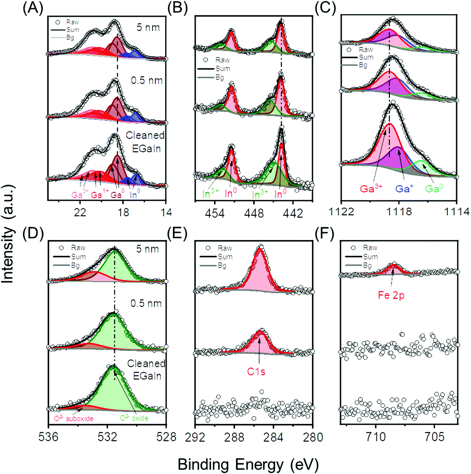 | ||
| Fig. 2 XPS core level spectra to show the growth of Fc–(CH2)14–Fc on GaOx/EGaIn films. In each panel, the data at the bottom represent GaOx/EGaIn films, the data in the middle and at the top represent GaOx/EGaIn films with 0.5 nm or 5 nm of Fc–(CH2)14–Fc, respectively, for (A) Ga 3d and In 4d, (B) In 3d, (C) Ga 2p3/2, (D) O 1s, (E) C 1s and (F) Fe 2p3/2. The absence of energy shifts in any of the core levels after molecule deposition could suggest that no charge transfer or covalent bonding takes place. | ||
Fig. 3A and B show the evolution of the Ga 2p3/2 and In 3d core levels, respectively, as a function of the Fc–(CH2)14–Fc thickness. The absence of shifts in the core levels of Ga or In after adsorption of Fc–(CH2)14–Fc could suggest that no covalent bonding or charge transfer between the GaOx/EGaIn film and Fc–(CH2)14–Fc takes place, although there have been a few examples where covalent bonds were formed without significant changes in core levels.77,78 This finding would be in agreement with the hypothesis that GaOx/EGaIn is chemically passive as mentioned in the Introduction. The results also indicate that the Ga/In ratio is about 8, implying that the GaOx layer predominantly consists of GaOx in agreement with previously reported results.16 We compare the decay of the Ga 2p signal and the growth of the C 1s signal (Fig. 3C) to the literature79 to understand the growth mode, and observe that the growth of the Fc–(CH2)14–Fc occurs in Stranski–Krastanov (layer plus island) mode. This mode of growth is a two-step process, where the initial film formation occurs in a layer-by-layer mode. After a critical thickness is reached, the growth of the film continues by nucleation on adsorbate islands. This mode is detected by steep linear growth of the C 1s signal in Fig. 3C until at around 0.5 nm the critical thickness is reached (regime 1 as indicated in the figure). Beyond this critical thickness, the C 1s signal grows linearly with a reduced slope that decreases with thickness and the signal growth resembles an inverted exponential function (regime 2).
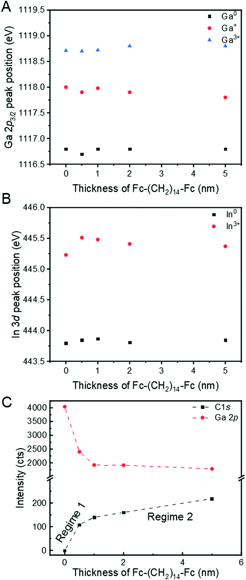 | ||
| Fig. 3 Peak position for core levels of (A) Ga 2p3/2 and (B) In 3d5/2 as a function of Fc–(CH2)14–Fc thickness, (C) Plot of intensity as a function of the deposited Fc–(CH2)14–Fc thickness for C 1s (black squares) and Ga 2p3/2 (red circles). The intensity evolution suggests a Stranski–Krastanov (layer plus islands) mode of growth of the Fc–(CH2)14–Fc layer, as represented by the dashed lines which show a layer-by-layer model of growth of Fc–(CH2)14–Fc till the critical thickness is achieved and island type growth onwards. | ||
UPS of Fc–(CH2)14–Fc on GaOx/EGaIn films
Fig. 4A shows the UPS data recorded from the EGaIn/GaOx film before and after adsorption of Fc–(CH2)14–Fc. The value of Φ of the clean EGaIn/GaOx films is 4.2–4.3 eV (black line) and decreases slightly by about 0.13 eV after deposition of 0.5 nm of Fc–(CH2)14–Fc. The small Φ reduction by this layer of Fc–(CH2)14–Fc is attributed to the so-called cushion or push-back effect, as typically observed for metals and metal oxides.6,18 After this initial change in Φ, the value of Φ remained constant with the deposition of additional layers Fc–(CH2)14–Fc of up to 5 nm, which suggests that no charge transfer occurs at the Fc‖GaOx/EGaIn interface. Fig. 4B shows the corresponding valence band (VB) spectrum of the cleaned GaOx/EGaIn film where the Fermi edge can be clearly seen as indicated. Notably, the surface exhibits tail states (indicated by the dashed ellipse) toward the Fermi-edge are clearly visible. These are expected given the defective nature of the GaOx layer, which consists of different gallium oxide phases, contains indium oxides and other defects (e.g., oxygen vacancies; see ref. 16 for more details). Such interface states may be important in the context of charge transfer with molecules other than those used here or provide additional tunnelling channels in molecular junctions.63,80 In the present case, however, the tails states are rather low in energy and no features are visible between EF and a binding energy of about 2 eV. The tail states become notable at binding energies of roughly >3.0 eV, which is far away from the bias window in typical charge transport studies involving EGaIn top electrodes. These observations reinforce our earlier conclusions19,59,62,63 that the GaOx layer is practically an electrical conductor. Below, we reinforce that there is no indication of charge transfer between Fc and the GaOx/EGaIn surface, implying that these tail states play no significant role in the present case.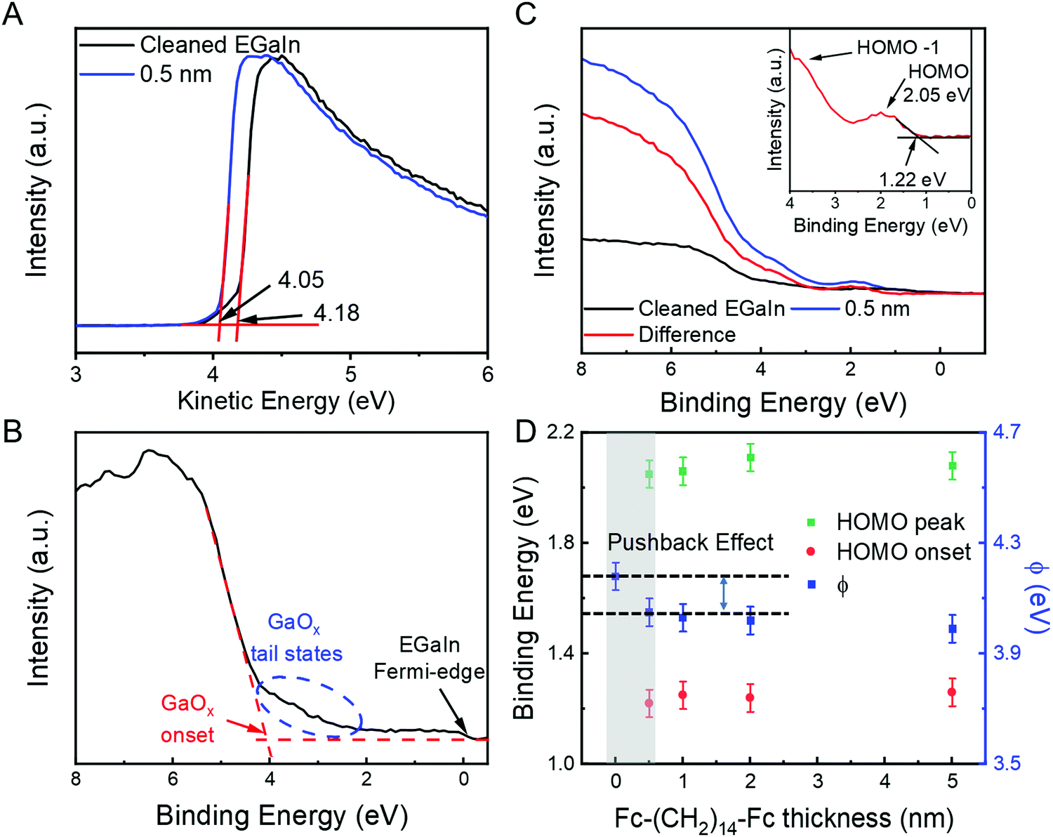 | ||
| Fig. 4 (A) The SECO spectra of cleaned GaOx/EGaIn (black) and after deposition of 0.5 nm Fc–(CH2)14–Fc (blue). The small work function reduction after initial deposition of Fc–(CH2)14–Fc is ascribed to the pushback effect. (B) VB spectra of cleaned GaOx/EGaIn measured with He II excitation. The blue ellipse marks the presence of tail states of the GaOx layer. (C) VB spectra of cleaned GaOx/EGaIn (black) and after deposition of 0.5 nm Fc–(CH2)14–Fc (blue) measured with He I excitation, as well as the difference of both (red). The inset shows a zoom-in of the Fc–(CH2)14–Fc HOMO. (D) The change in HOMO level, HOMO onset and Φ as a function of the thickness of the Fc–(CH2)14–Fc deposited on the GaOx/EGaIn film. The pushback effect explains the 0.2 eV shift in the Φ upon deposition of 0.5 nm of the Fc–(CH2)14–Fc derivative onto GaOx/EGaIn films. | ||
Fig. 4C shows VB spectrum after the deposition of 0.5 nm of Fc–(CH2)14–Fc. We observe that three features become apparent with a binding energy of 2 eV, ∼4 eV and 6–8 eV. The lowest binding energy peaks can be readily assigned to the HOMO, HOMO−1 and HOMO−2 levels (with possible contributions from the HOMO of the alkyl chain and the valence band of the GaOx/EGaIn) of Fc–(CH2)14–Fc and are in very good agreement with UPS gas phase measurements of Fc.81 These results indicate that the interaction between the Fc and the GaOx/EGaIn is weak and imply that the aforementioned tail states do not induce any charge transfer between the Fc units and the surface. The energy of the HOMO onset is at a binding energy of 1.22 eV, resulting in a EHOMO (ionisation energy) of 5.27 eV for Fc–(CH2)14–Fc, in good agreement with previous PES measurements of Fc on Si,82 Fc SAMs on Au,55 and with the Fc SAMs on Au where EHOMO was determined with cyclic voltammetry.83
Table 1 summarises the HOMO level, HOMO onset (or the ΔE) and the Φ as a function of the thickness of the Fc–(CH2)14–Fc layer and Fig. 4D shows the corresponding plots. The uncertainty within the measurements is ∼50 meV, and all the measured energy level shifts are within the error. The value of ΔE and EHOMO are rather insensitive to the thickness of Fc–(CH2)14–Fc. The push-back effect is also described in the Fig. 4D, and an independent experiment to verify the push-back effect is discussed below. These results corroborate with the XPS results and confirm that Fc interacts weakly with the GaOx/EGaIn surface.
To verify that the shift in Φ is indeed due to the push-back effect, we investigated a 2 nm thick film of tetratetracontane (TTC), which is inert and wide-gap so that charge transfer with a clean GaOx/EGaIn surface can be ruled out on general grounds. Fig. 5A shows the SECO spectra for a clean GaOx/EGaIn film and the same film after deposition of 2 nm of TTC. We observe a shift in Φ of ∼0.2 eV for the GaOx/EGaIn films after adsorption of TTC. This shift is essentially the same as shown in Fig. 4A for Fc–(CH2)14–Fc, confirming our assumption that the ΔΦ after Fc–(CH2)14–Fc adsorption is driven by charge-rearrangements induced by the push-back effect and that no charge transfer occurs between the Fc and the GaOx/EGaIn surface. Fig. 5B shows the VB spectra for a cleaned GaOx/EGaIn film and after deposition of 2 nm of TTC. The alkane HOMO is not seen in our measurements, likely due to high density of states of the GaOx/EGaIn layer which, consequently, dominates the spectrum. For the sake of completion, a wide scan XPS of 2.0 nm thick TTC/GaOx/EGaIn and is shown in Fig. S14 (ESI†) with the C 1s spectra. We observe a C 1s peak at ∼285.3 eV in Fig. S14B (ESI†) that confirms the presence of the TTC. The C 1s peak for TTC is almost indistinguishable from the C 1s peak of the Fc and highlights that the C sp2 and sp3 contributions could not be reasonably distinguished with our setup.
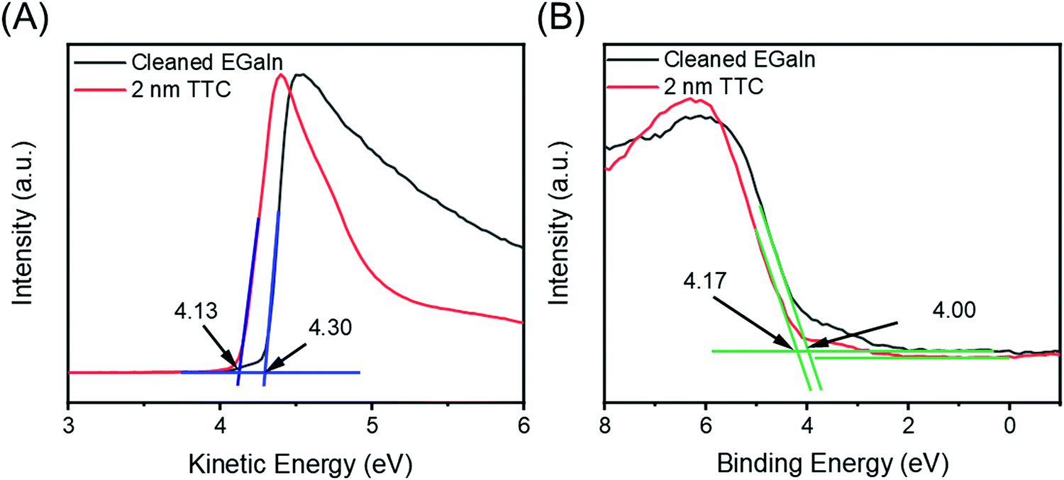 | ||
| Fig. 5 (A) The SECO and (B) VB spectra for a clean GaOx/EGaIn film (black) and after deposition of 2 nm TTC (red). The cut-off positions and HOMO or VB onsets are marked with blue and green bars, respectively. The Φ and HOMO or VB onset energies are denoted alongside. | ||
Charge transport measurements
The previous sections describe the energy level alignment of the Fc‖GaOx/EGaIn interface, in this section we use this knowledge to improve our understanding to the energy level alignment of Ag–S(CH2)11Fc‖GaOx/EGaIn junctions (Fig. 1A). The mechanism of rectification in these junctions has been elaborated previously.55 Briefly, charge transport under the positive bias is mediated by off-resonant tunnelling. The HOMO is localised on the Fc unit and enters the bias window under a negative applied bias and charge transport transitions to an incoherent tunnelling regime with relatively higher tunnelling currents, resulting in ∼100-fold increase in the tunnelling current only at V = −1.0 V.To compare the photoelectron spectroscopy studies with in situ junction characterisation, we formed junctions of Ag–S(CH2)11Fc‖GaOx/EGaIn with cone-shaped EGaIn tips as the top electrode. We measured five traces with step size of 10 mV, Fig. 6A shows the average J(V) curves for the traces, the shape of which is very similar as previously reported curves.55 We used normalised Differential Conductance (NDC) analysis to enhance voltage-induced changes in conductance. Based on the shape of NDC curves, we can identify the transport characteristics of the junctions and understand whether charge transport is dominated by off-resonant or resonant tunnelling.41 The parabolic shape of the J(V) curves and peaks of the NDC curve are characteristic of off-resonant tunnelling and resonant tunnelling, where the MOs participate in the charge transport.84 The NDC is defined as:41
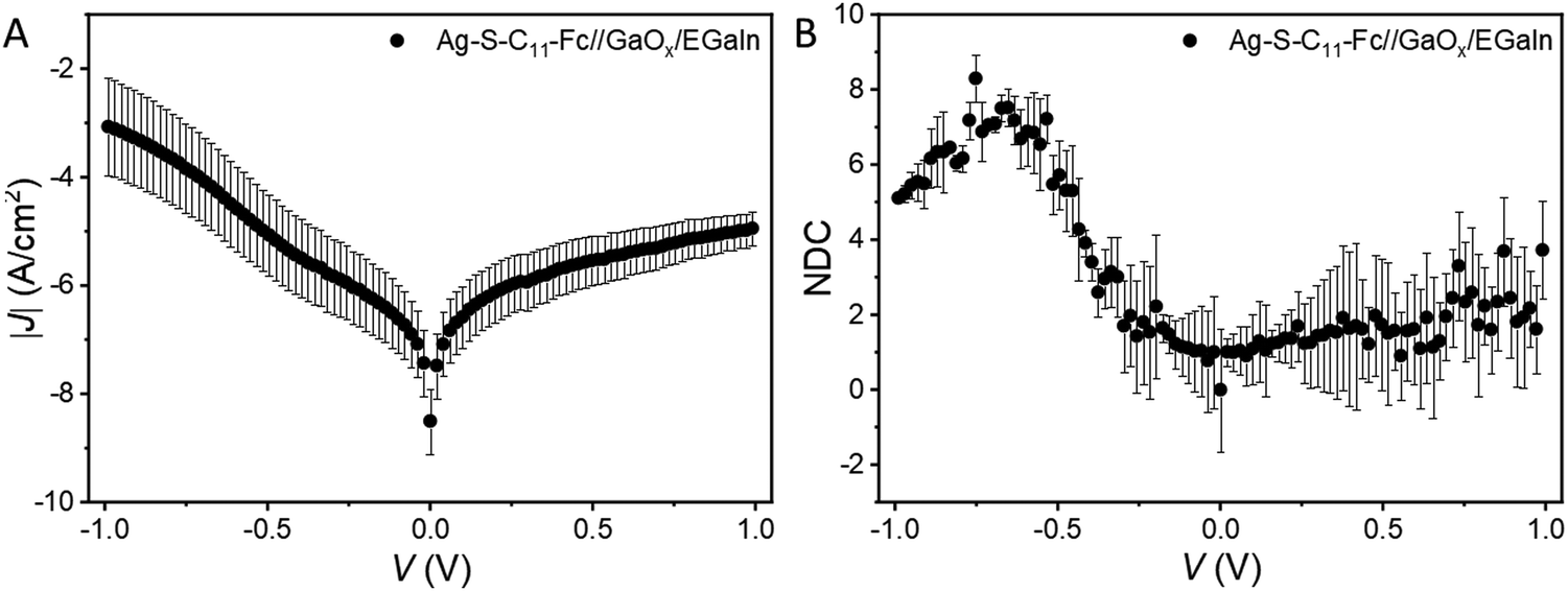 | ||
| Fig. 6 (A) Shows an average of |J| vs. V measurement on an Ag-S-C11-Fc‖GaOx/EGaIn molecular diode, which is subsequently smoothened by a moving smoothening function to obtain the derivative which is used to obtain the (B) NDC plot for the measurement, error bar: standard deviation for 5 scans. | ||
In principle, the NDC- and PES-detected HOMO should be comparable. We note that the ΔEPES for 0.5 nm Fc–(CH2)14–Fc deposited on the GaOx/EGaIn films is 1.22 ± 0.05 eV (Fig. 4B). In refs 55 and 85, we have reported before the offset in energy between the HOMO of the Fc and Fermi level of the Au electrode of ferrocenyl alkanethiolate SAMs of 1.0–1.2 eV with UPS (ΔEPES).55,85 Thus, we observe that the ΔE values obtained by PES and NDC are different, and the differences are attributed to the polarisation of the molecules by the EGaIn electrode and the metal-induced broadening of the molecule's energy levels, which is induced by the metal even in physisorptive systems.86 Both effects cause a reduction of the HOMO–LUMO gap. The reduction of the HOMO–LUMO gap can be quantified by the energy renormalisation factor (≈ΔEPES/ΔEjunction) and from our data, we obtain an energy renormalisation factor of ∼2 for our Ag–S–C11–Fc‖GaOx/EGaIn junctions. This value is very close to earlier suggested values of 1.5–2.0.28,87 It is important to note that this value is far below the 10–25 fold renormalisation factor observed in electromigration break junctions,3,9,30–32 from which we conclude that GaOx/EGaIn junctions operate in the weak coupling regime.
Conclusions
The major conclusion of this work is that the top electrode in EGaIn junctions interacts weakly with Fc-based SAMs, and charge transfer or chemical reactions between the GaOx/EGaIn surface and Fc do not occur. This work validates the assumption that GaOx/EGaIn forms weakly coupled contacts to such SAMs and, therefore, the energy level alignment estimation via ex situ techniques with the SAMs in contact with vacuum or an electrolyte give a reasonable estimate of the energy level alignment in the junction. We have claimed before that in large-area EGaIn junctions the renormalisation factor is as small as 1.5–2.0;28,87 in this work, we confirm that the renormalisation factor is ∼2. Ferrocene is a moderate electron donor and future studies should aim to investigate whether these assumptions also hold for junctions with monolayers comprising stronger electron donors or acceptors. Although it is fairly common to study in detail the bottom electrode–molecule interaction, the interaction between the molecule and the top electrode is usually not explicitly studied. We hope that this work will also stimulate others to investigate the molecule top-electrode interaction involving other types of top electrode materials. Such investigations would help to improve our understanding of charge transport across the various types of molecular junctions and allow for quantitative comparisons between different platforms.Conflicts of interest
There are no conflicts to declare.Acknowledgements
The work in Berlin was supported by the Deutsche Forschungsgemeinschaft (DFG) – Projektnummer 182087777 – SFB 951. Dr Yiliang Lin and Prof. Michael Dickey (North Carolina State University) are acknowledged for helpful advice and discussions. The Prime Minister's Office, Singapore, under its medium-sized centre program, is acknowledged for supporting this research.References
- D. Xiang, X. Wang, C. Jia, T. Lee and X. Guo, Chem. Rev., 2016, 116, 4318 CrossRef CAS PubMed.
- A. Vilan, D. Aswal and D. Cahen, Chem. Rev., 2017, 117, 4248 CrossRef CAS PubMed.
- C. J. O. Verzijl, J. A. Celis Gil, M. L. Perrin, D. Dulić, H. S. J. van der Zant and J. M. Thijssen, J. Chem. Phys., 2015, 143, 174106 CrossRef CAS PubMed.
- C. Jia and X. Guo, Chem. Soc. Rev., 2013, 42, 5642 RSC.
- C. J. Lambert, Chem. Soc. Rev., 2015, 44, 875 RSC.
- G. Heimel, L. Romaner, E. Zojer and J.-L. L. Bredas, Acc. Chem. Res., 2008, 41, 721 CrossRef CAS PubMed.
- G. Heimel, S. Duhm, I. Salzmann, A. Gerlach, A. Strozecka, J. Niederhausen, C. Bürker, T. Hosokai, I. Fernandez-Torrente, G. Schulze, S. Winkler, A. Wilke, R. Schlesinger, J. Frisch, B. Bröker, A. Vollmer, B. Detlefs, J. Pflaum, S. Kera, K. J. Franke, N. Ueno, J. I. Pascual, F. Schreiber and N. Koch, Nat. Chem., 2013, 5, 187 CrossRef CAS PubMed.
- G. Heimel, L. Romaner, E. Zojer and J.-L. Brédas, Nano Lett., 2007, 7, 932 CrossRef CAS PubMed.
- M. L. Perrin, C. J. O. O. Verzijl, C. A. Martin, A. J. Shaikh, R. Eelkema, J. H. van Esch, J. M. Van Ruitenbeek, J. M. Thijssen, H. S. J. J. Van Der Zant and D. Dulić, Nat. Nanotechnol., 2013, 8, 282 CrossRef CAS PubMed.
- B. Xu and N. Tao, Science, 2003, 301, 1221 CrossRef CAS PubMed.
- G. Wang, Y. Kim, M. Choe, T.-W. Kim and T. Lee, Adv. Mater., 2011, 23, 755 CrossRef CAS PubMed.
- H. B. Akkerman, P. W. M. Blom, D. M. de Leeuw and B. de Boer, Nature, 2006, 441, 69 CrossRef CAS PubMed.
- H. Yan, A. J. Bergren and R. L. McCreery, J. Am. Chem. Soc., 2011, 133, 19168 CrossRef CAS PubMed.
- B. Kayser, J. A. Fereiro, R. Bhattacharyya, S. R. Cohen, A. Vilan, I. Pecht, M. Sheves and D. Cahen, J. Phys. Chem. Lett., 2020, 11, 144 CrossRef CAS PubMed.
- E. P. Honig, Thin Solid Films, 1976, 33, 231 CrossRef CAS.
- L. Cademartiri, M. M. Thuo, C. A. Nijhuis, W. F. Reus, S. Tricard, J. R. Barber, R. N. S. Sodhi, P. Brodersen, C. Kim, R. C. Chiechi and G. M. Whitesides, J. Phys. Chem. C, 2012, 116, 10848 CrossRef CAS.
- R. C. Chiechi, E. A. Weiss, M. D. Dickey and G. M. Whitesides, Angew. Chem., Int. Ed., 2008, 47, 142 CrossRef CAS PubMed.
- N. Koch, A. Kahn, J. Ghijsen, J.-J. Pireaux, J. Schwartz, R. L. Johnson and A. Elschner, Appl. Phys. Lett., 2003, 82, 70 CrossRef CAS.
- J. Hwang, A. Wan and A. Kahn, Mater. Sci. Eng., R, 2009, 64, 1 CrossRef.
- X. Crispin, V. Geskin, A. Crispin, J. Cornil, R. Lazzaroni, W. R. Salaneck and J.-L. Brédas, J. Am. Chem. Soc., 2002, 124, 8131 CrossRef CAS PubMed.
- S. Mukhopadhyay, S. K. Karuppannan, C. Guo, J. A. Fereiro, A. Bergren, V. Mukundan, X. Qiu, O. E. Castañeda Ocampo, X. Chen, R. C. Chiechi, R. McCreery, I. Pecht, M. Sheves, R. R. Pasula, S. Lim, C. A. Nijhuis, A. Vilan and D. Cahen, iScience, 2020, 23, 101099 CrossRef CAS PubMed.
- Z. Xie, I. Bâldea and C. D. Frisbie, J. Am. Chem. Soc., 2019, 141, 18182 CrossRef CAS PubMed.
- Z. Xie, I. Bâldea and C. D. Frisbie, J. Am. Chem. Soc., 2019, 141, 3670 CrossRef CAS PubMed.
- A. Nitzan, M. Galperin, G.-L. Ingold and H. Grabert, J. Chem. Phys., 2002, 117, 10837 CrossRef CAS.
- Y. Han, C. Nickle, Z. Zhang, H. P. A. G. Astier, T. J. Duffin, D. Qi, Z. Wang, E. del Barco, D. Thompson and C. A. Nijhuis, Nat. Mater., 2020, 19, 843 CrossRef CAS PubMed.
- T. A. Su, M. Neupane, M. L. Steigerwald, L. Venkataraman and C. Nuckolls, Nat. Rev. Mater., 2016, 1, 16002 CrossRef CAS.
- B. Kim, S. H. Choi, X.-Y. Zhu and C. D. Frisbie, J. Am. Chem. Soc., 2011, 133, 19864 CrossRef CAS PubMed.
- L. Yuan, R. Breuer, L. Jiang, M. Schmittel and C. A. Nijhuis, Nano Lett., 2015, 15, 5506 CrossRef CAS PubMed.
- A. Vilan, ECS Trans., 2018, 86, 67 CrossRef CAS.
- J. M. Garcia-Lastra, C. Rostgaard, A. Rubio and K. S. Thygesen, Phys. Rev. B: Condens. Matter Mater. Phys., 2009, 80, 245427 CrossRef.
- K. S. Thygesen and A. Rubio, Phys. Rev. Lett., 2009, 102, 1 CrossRef PubMed.
- J. A. Celis Gil and J. M. Thijssen, J. Chem. Phys., 2017, 147, 084102 CrossRef CAS PubMed.
- R. Kuhrt, M. Hantusch, M. Knupfer and B. Büchner, Surf. Interface Anal., 2020, 52, 953 CrossRef CAS.
- H. Wang, S. V. Levchenko, T. Schultz, N. Koch, M. Scheffler and M. Rossi, Adv. Electron. Mater., 2019, 5, 1800891 CrossRef.
- R. Otero, A. L. Vázquez de Parga and J. M. Gallego, Surf. Sci. Rep., 2017, 72, 105 CrossRef CAS.
- J. M. Beebe, B. Kim, J. W. Gadzuk, C. Daniel Frisbie and J. G. Kushmerick, Phys. Rev. Lett., 2006, 97, 026801 CrossRef PubMed.
- G. Ricœur, S. Lenfant, D. Guérin and D. Vuillaume, J. Phys. Chem. C, 2012, 116, 20722 CrossRef.
- F. Mirjani, J. M. Thijssen and S. J. van der Molen, Phys. Rev. B: Condens. Matter Mater. Phys., 2011, 84, 115402 CrossRef.
- K. Smaali, S. Lenfant, S. Karpe, M. Oçafrain, P. Blanchard, D. Deresmes, S. Godey, A. Rochefort, J. Roncali and D. Vuillaume, ACS Nano, 2010, 4, 2411 CrossRef CAS PubMed.
- E. H. Huisman, C. M. Guédon, B. J. van Wees and S. J. van der Molen, Nano Lett., 2009, 9, 3909 CrossRef CAS PubMed.
- A. Vilan, Phys. Chem. Chem. Phys., 2017, 19, 27166 RSC.
- A. Vilan, D. Cahen and E. Kraisler, ACS Nano, 2013, 7, 695 CrossRef CAS PubMed.
- J. Chen, M. Kim, S. Gathiaka, S. J. Cho, S. Kundu, H. J. Yoon and M. M. Thuo, J. Phys. Chem. Lett., 2018, 9, 5078 CrossRef CAS PubMed.
- J. Chen, S. Gathiaka, Z. Wang and M. Thuo, J. Phys. Chem. C, 2017, 121, 23931 CrossRef CAS.
- M. Baghbanzadeh, L. Belding, L. Yuan, J. Park, M. H. Al-Sayah, C. M. Bowers and G. M. Whitesides, J. Am. Chem. Soc., 2019, 141, 8969 CrossRef CAS PubMed.
- H. J. Yoon, C. M. Bowers, M. Baghbanzadeh and G. M. Whitesides, J. Am. Chem. Soc., 2014, 136, 16 CrossRef CAS PubMed.
- S. Park and H. J. Yoon, Nano Lett., 2018, 18, 7715 CrossRef CAS PubMed.
- S. Park, N. Cho and H. J. Yoon, Chem. Mater., 2019, 31, 5973 CrossRef CAS.
- D. Fracasso, H. Valkenier, J. C. Hummelen, G. C. Solomon and R. C. Chiechi, J. Am. Chem. Soc., 2011, 133, 9556 CrossRef CAS.
- S. Kumar, M. Merelli, W. Danowski, P. Rudolf, B. L. Feringa and R. C. Chiechi, Adv. Mater., 2019, 31, 1807831 CrossRef PubMed.
- M. Carlotti, S. Soni, S. Kumar, Y. Ai, E. Sauter, M. Zharnikov and R. C. Chiechi, Angew. Chem., Int. Ed., 2018, 57, 15681 CrossRef CAS PubMed.
- W. Du, Y. Han, H. Hu, H.-S. Chu, H. V. Annadata, T. Wang, N. Tomczak and C. A. Nijhuis, Nano Lett., 2019, 19, 4634 CrossRef CAS PubMed.
- M. J. Regan, P. S. Pershan, O. M. Magnussen, B. M. Ocko, M. Deutsch and L. E. Berman, Phys. Rev. B: Condens. Matter Mater. Phys., 1997, 55, 15874 CrossRef CAS.
- M. F. Dumke, T. A. Tombrello, R. A. Weller, R. M. Housley and E. H. Cirlin, Surf. Sci., 1983, 124, 407 CrossRef CAS.
- L. Yuan, N. Nerngchamnong, L. Cao, H. Hamoudi, E. Del Barco, M. Roemer, R. K. Sriramula, D. Thompson and C. A. Nijhuis, Nat. Commun., 2015, 6, 1 Search PubMed.
- N. Nerngchamnong, L. Yuan, D.-C. Qi, J. Li, D. Thompson and C. A. Nijhuis, Nat. Nanotechnol., 2013, 8, 113 CrossRef CAS PubMed.
- L. Yuan, L. Jiang, D. Thompson and C. A. Nijhuis, J. Am. Chem. Soc., 2014, 136, 6554 CrossRef CAS PubMed.
- D. Thompson, E. Del Barco and C. A. Nijhuis, Appl. Phys. Lett., 2020, 117, 030502 CrossRef CAS.
- S. K. Karuppannan, H. Hongting, C. Troadec, A. Vilan and C. A. Nijhuis, Adv. Funct. Mater., 2019, 29, 1904452 CrossRef.
- C. A. Nijhuis, W. F. Reus and G. M. Whitesides, J. Am. Chem. Soc., 2010, 132, 18386 CrossRef CAS PubMed.
- C. A. Nijhuis, W. F. Reus, A. C. Siegel and G. M. Whitesides, J. Am. Chem. Soc., 2011, 133, 15397 CrossRef CAS PubMed.
- M. J. Regan, H. Tostmann, P. S. Pershan, O. M. Magnussen, E. DiMasi, B. M. Ocko and M. Deutsch, Phys. Rev. B: Condens. Matter Mater. Phys., 1997, 55, 10786 CrossRef CAS.
- A. Kahn, N. Koch and W. Gao, J. Polym. Sci., Part B: Polym. Phys., 2003, 41, 2529 CrossRef CAS.
- E. P. Yalcintas, K. B. Ozutemiz, T. Cetinkaya, L. Dalloro, C. Majidi and O. B. Ozdoganlar, Adv. Funct. Mater., 2019, 29, 1906551 CrossRef CAS.
- E. H. Kawamoto, S. Lee, P. S. Pershan, M. Deutsch, N. Maskil and B. M. Ocko, Phys. Rev. B: Condens. Matter Mater. Phys., 1993, 47, 6847 CrossRef CAS PubMed.
- X. Chen, M. Roemer, L. Yuan, W. Du, D. Thompson, E. Del Barco and C. A. Nijhuis, Nat. Nanotechnol., 2017, 12, 797 CrossRef CAS PubMed.
- C. S. S. Sangeeth, A. Wan and C. A. Nijhuis, J. Am. Chem. Soc., 2014, 136, 11134 CrossRef CAS PubMed.
- K.-F. Braun, V. Iancu, N. Pertaya, K.-H. Rieder and S.-W. Hla, Phys. Rev. Lett., 2006, 96, 246102 CrossRef PubMed.
- P. Dowben, C. Waldfried, T. Komesu, D. Welipitiya, T. McAvoy and E. Vescovo, Chem. Phys. Lett., 1998, 283, 44 CrossRef CAS.
- P. J. Durston and R. E. Palmer, Surf. Sci., 1998, 400, 277 CrossRef CAS.
- D. Y. Zhong, W. C. Wang, R. F. Dou, K. Wedeking, G. Erker, L. F. Chi and H. Fuchs, Phys. Rev. B: Condens. Matter Mater. Phys., 2007, 76, 205428 CrossRef.
- A. Tabatabai, A. Fassler, C. Usiak and C. Majidi, Langmuir, 2013, 29, 6194 CrossRef CAS PubMed.
- X. Chen, H. Hu, J. Trasobares and C. A. Nijhuis, ACS Appl. Mater. Interfaces, 2019, 11, 21018 CrossRef CAS PubMed.
- F. Scharmann, G. Cherkashinin, V. Breternitz, C. Knedlik, G. Hartung, T. Weber and J. A. Schaefer, Surf. Interface Anal., 2004, 36, 981 CrossRef CAS.
- H. Iwakuro, C. Tatsuyama and S. Ichimura, Jpn. J. Appl. Phys., 1982, 21, 94 CrossRef CAS.
- M. Barber, J. A. Connor, L. M. R. Derrick, M. B. Hall and I. H. Hillier, J. Chem. Soc., Faraday Trans. 2, 1973, 559 RSC.
- K. Heister, M. Zharnikov, M. Grunze and L. S. O. Johansson, J. Phys. Chem. B, 2001, 105, 4058 CrossRef CAS.
- F. Chesneau, J. Zhao, C. Shen, M. Buck and M. Zharnikov, J. Phys. Chem. C, 2010, 114, 7112 CrossRef CAS.
- M. Heuberger, G. Dietler and L. Schlapbach, Surf. Sci., 1994, 314, 13 CrossRef CAS.
- A. Vilan and D. Cahen, Chem. Rev., 2017, 117, 4624 CrossRef CAS PubMed.
- C. Cauletti, J. C. Green, M. R. Kelly, P. Powell, J. van Tilborg, J. Robbins and J. Smart, J. Electron Spectrosc. Relat. Phenom., 1980, 19, 327 CrossRef CAS.
- R. Zanoni, M. N. Piancastelli, M. Marsi and G. Margaritondo, J. Electron Spectrosc. Relat. Phenom., 1991, 57, 199 CrossRef CAS.
- N. Nerngchamnong, D. Thompson, L. Cao, L. Yuan, L. Jiang, M. Roemer and C. A. Nijhuis, J. Phys. Chem. C, 2015, 119, 21978 CrossRef CAS.
- Y. Han, M. S. Maglione, V. Diez Cabanes, J. Casado-Montenegro, X. Yu, S. K. Karuppannan, Z. Zhang, N. Crivillers, M. Mas-Torrent, C. Rovira, J. Cornil, J. Veciana and C. A. Nijhuis, ACS Appl. Mater. Interfaces, 2020, 12, 55044 CrossRef CAS PubMed.
- L. Jiang, C. S. S. Sangeeth, A. Wan, A. Vilan and C. A. Nijhuis, J. Phys. Chem. C, 2015, 119, 960 CrossRef CAS.
- H. Vázquez, R. Oszwaldowski, P. Pou, J. Ortega, R. Pérez, F. Flores and A. Kahn, Europhys. Lett., 2004, 65, 802 CrossRef.
- A. R. Garrigues, L. Yuan, L. Wang, E. R. Mucciolo, D. Thompon, E. del Barco and C. A. Nijhuis, Sci. Rep., 2016, 6, 26517 CrossRef CAS.
Footnotes |
| † Electronic supplementary information (ESI) available. See DOI: 10.1039/d1cp01690c |
| ‡ These authors contributed equally to this work. |
| This journal is © the Owner Societies 2021 |