
 Open Access Article
 This Open Access Article is licensed under a Creative Commons Attribution-Non Commercial 3.0 Unported Licence
Electromechanically active pair dynamics in a Gd-doped ceria single crystal†
Simone
Santucci
 *a,
Haiwu
Zhang
a,
Ahsanul
Kabir
a,
Carlo
Marini
b,
Simone
Sanna
a,
Jyn Kyu
Han
a,
Gregor
Ulbrich
c,
Eva Maria
Heppke
c,
Ivano E.
Castelli
a and
Vincenzo
Esposito
*a
*a,
Haiwu
Zhang
a,
Ahsanul
Kabir
a,
Carlo
Marini
b,
Simone
Sanna
a,
Jyn Kyu
Han
a,
Gregor
Ulbrich
c,
Eva Maria
Heppke
c,
Ivano E.
Castelli
a and
Vincenzo
Esposito
*a
aDepartment of Energy Conversion and Storage, Technical University of Denmark, Fysikvej, Building 310, 2800 Kgs., Lyngby, Denmark. E-mail: vies@dtu.dk; sisan@dtu.dk
bALBA Synchrotron, Carrer de la llum, 2-26Cerdanyola del Vallès, 08290 Barcelona, Spain
cInstitut für Chemie, Technische Universität Berlin, Straße des 17, Juni 135, 10623 Berlin, Germany
First published on 20th April 2021
Abstract
Oxygen-defective ceria, e.g. Gd-doped ceria, shows giant electromechanical properties related to a complex local rearrangement of its lattice. Although they are not entirely identified, the electroactive mechanisms arise from cation and oxygen vacancy (VO) pairs (i.e. Ce–VO), and the local structural elastic distortion in their surroundings. Here, we study the geometry and behaviour of Ce–VO pairs in a grain boundary-free bulk Ce0.9Gd0.1O1.95 single crystal under an AC electric field of ca. 11 kV cm−1. The analysis was carried out through X-ray absorption spectroscopy (XAS) techniques at the Ce L-III edge. Using Density Functional Theory (DFT) calculations, we investigated the effects of the strain on density of states and orbitals at the valence band edge. Our research indicates that electrostriction increases at low temperatures. The electromechanical strain has a structural nature and can rise by one order of magnitude, i.e., from 5 × 10⁻⁴ at room temperature to 5 × 10⁻³ at −193 °C, due to an increase in the population of the electrically active pairs. At a constant VO concentration, the material can thus configure heterogeneous pairs and elastic nanodomains that are either mechanically responsive or not.
Introduction
Gadolinium-doped ceria (CGO) and other oxygen-defective oxides have recently attracted attention for their outstanding “non-classical” giant electrostriction.1–5 However, the electromechanical mechanisms in the materials remain unclear. Several studies have used X-ray Absorption Spectroscopy (XAS) to show the dynamics of non-classical electrostriction related to the defect structure of the CGO lattice.1,6,7 Doped ceria accommodates many randomly distributed double-positive oxygen vacancies (VO, i.e. , according to the Kröger–Vink notation). Doping the material with 20 mol% Gd3+ produces an oxygen vacancy concentration of 10% while maintaining the cubic fluorite symmetry of the lattice.8–10 At such a high doping level, the vacancy concentration depends only on the extrinsic dopant amount, and so it is considered constant.
Each oxygen vacancy causes a local electro-steric distortion and a deviation in the lattice. At the first level of analysis, the CeCe–VO pairs impose local elastic and charge fields1,6 which relax through the crystal. When an electric field is applied, both the CeCe–VO pair and the cluster in its vicinity experience strain, leading to a macroscopic expansion.6,11 Such an effect is different from “classical” electrostriction mechanisms, proposed by Newnham, where the distortion comprises the whole structure.11 As a result, CGO and other defective fluorites can display outstanding electrostrictive behaviour.
The definition of CeCe–VO includes both 4+ host cations ([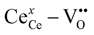 ]) and the polarised 3+ species-vacancies pairs ([
 ] and the [
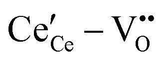 ]). However, assuming that the oxygen defects are random in the lattice and their mobility is nearly null at low temperature, CeCe–VO pairs embody the average of all the configurations in the crystal.
For epitaxial thin CGO films with controlled orientation, the electrostriction coefficient, e.g. M33, is between 10−17 and 10−16 m2 V−2.11 This value surpasses the best piezoelectric electrostrictor, Pb(Mn1/3Nb2/3)O3 (PMN), which has typical M33 values of 10−18 m2 V−2.12 In epitaxial films, electrostriction is enhanced by aligning the applied electric field to the CeCe–VO pairs.11 In polycrystalline thin films1–3,5,13 and bulk ceramics,4,14 the presence of grain boundaries and disorder leads to randomly oriented CeCe–VO pairs. Further, crystalline disorder introduces a wide range of electrosteric factors with a complex variety of configurations and electromechanical responses.14
The vacancy's elastic response to an electric field is indeed related to the temperature.10,15–17 In thin-films, electrostrictive performances do not change from 25° to 75 °C.18,19 However, at high temperatures, defects diffuse in the lattice,20,21 hindering electrostriction and leading to ionic conduction.1,18,19 Simultaneously with vacancy mobility, there is an increase of secondary “non-structural” effects such as asymmetric electrode polarisation, chemical reactions and charge injection at the film/electrode interface.18 These side-processes hinder a clear definition of the driving mechanisms in electrostriction, reducing performance and often leading to the mechanical failure of these materials.1,3,19
Electrostriction measurements at low temperatures are still not available in the literature. However, the suppression of thermally driven mechanisms can help the analysis of this phenomenon. Some studies have already unveiled some other typical oxygen vacancies and CeCe–VO pair effects at low temperatures.6,14,22,23 In CGO thin films, cooling to −123 °C leads to a reduction of the dielectric constant as charge-hopping decreases (exponentially).22 For temperatures below −200 °C,22 the dielectric constant of CGO is both temperature- and frequency-independent, with a value of εr = 20 ± 2. Such an effect likely arises from low temperature triggered fluctuations in the ordering of the CeCe–VO pairs.22 Such a feature is particularly relevant for electrostriction; if the total concentration of the vacancies is kept constant, pairs and their domains can change their configuration in the presence of intense electric fields. Local lattice distortions also occur in bulk ceria doped with other trivalent cations (Y or Sc). At low temperatures of about −160 °C, such a structural distortion arises from an asymmetry in the cation/anion pair potential.23 This kind of distortion likely comprises a broader cluster of atoms, leading to nanodomain-like effects. Moreover, the cage of eight O2− ions surrounding the dopant cation assumes an asymmetrical configuration.23 As electrostriction in CGO results from lattice distortions around the oxygen vacancy,6,14 low-temperature dynamics are likely to influence the mechanisms which produce this effect.
In the present paper, we investigate the structural and chemical environments in the vicinity of vacancies by X-ray Absorption Spectroscopy (XAS). We report the electrostriction property of 10 mol% Gd-doped CeO2 in a single crystal, i.e. free of pair-disorder electrosteric interactions at a constant concentration (extrinsic conditions). We use X-ray absorption techniques to characterize the local distortion dynamics behaviour of Ce–O chains under an electric field over a wide temperature range (from RT down to −194 °C). We apply in situ an electric field to clarify the CeO2 crystalline cell's effect towards the geometrical deformation caused by Ce–O bond length non-constant distribution around the defects.6,7 Such results give new insights into the mechanism of the outstanding non-classic electrostriction properties in this family of materials.
Experimental
Single crystal synthesis
A 10 mol% CGO single crystal (CGO20) was grown using the skull melting technique. Details are reported for zirconia and ceria in other papers.24–27 The sample selected for the test was 4 × 4 × 0.7 mm thick, with gold electrodes sputtered on two opposite faces normal to the [111] direction.Structural, electrical and electrostriction characterization
We performed ex situ electrostriction measurements at room temperature via laser interferometry microscopy (Nano Vibration Analyzer – SIOS Meßtechnik GmbH) (Fig. S1, ESI†). Details of the experimental setup and configurations are in the ESI.†![[thin space (1/6-em)]](https://www.rsc.org/images/entities/char_2009.gif) 3,11 Sample investigation included X-ray diffraction (Fig. S2, ESI†) and electrochemical impedance spectroscopy (Fig. S3, ESI†). Experimental details on impedance spectroscopy method are in a previous publication.14
3,11 Sample investigation included X-ray diffraction (Fig. S2, ESI†) and electrochemical impedance spectroscopy (Fig. S3, ESI†). Experimental details on impedance spectroscopy method are in a previous publication.14
X-Ray absorption spectroscopy
For the XAS analysis, we performed the experiments at the Claess beamline in Elettra synchrotron. The experimental details can be found in the literature.28 The experiments were performed at the Ce L-III-edge (≈5.7 keV) on a CGO single crystal in fluorescence mode, using a Si(111) double crystal monochromator with a flux of 1012 photons per sec. We acquired data with a multi-channel SDD that allows up to six spectra for each measurement. 15–20 acquisitions were used for the analysis, each performed with all six available channels merged to increase the signal/noise ratio. The energy resolution was 0.3 eV. The spectra were normalized using the Athena and Artemis software, within the IFEFFIT package.29 For the temperature control, we conditioned the sample in a cryostat,28,30,31 cooling with a liquid nitrogen line (LN2-cryo) passed through the sample holder. The pressure was set to P ≈ 10−3 mbar to maintain the X-ray beam intensity.Fig. 1 shows the schematics of the experimental setup. The measurements started at RT and then the sample was cooled to −193 °C, and progressively at −125 °C, −50 °C and 23 °C (RT) at 2 °C min−1. At each temperature, the sample was first equilibrated for 30 min, followed by the XAS measurement without an electric field (“OFF” state) and then with an electric field applied (11 kV cm−1 in the “ON” state). We recorded 24–30 XAS spectra in each state, which were then normalized and merged using Athena software.29 The final data sets include two spectra (ON and OFF) for each temperature. We used a solid-state detector (Amptek silicon drift (XR-100SDD)) placed at 90 degrees to the incoming beam.28 The monochromator is a liquid nitrogen-cooled double-crystal FMB-Oxford, Si 111-crystal. The source was a 1 m long wiggler with 25 NdFeB poles. The maximum field was 1.74 T, and the minimum gap was 12.9 mm. The theoretical maximum energy was 70 keV. We applied the electric field with an AIM-TTI TGP 3100 function generator coupled with a Trek 2220 amplifier, which supplied a maximum voltage of 2 kV. To contact the samples inside the chamber, we used cables passed through a vacuum valve with BHV contact on the outside and solder contact inside the cryostat.
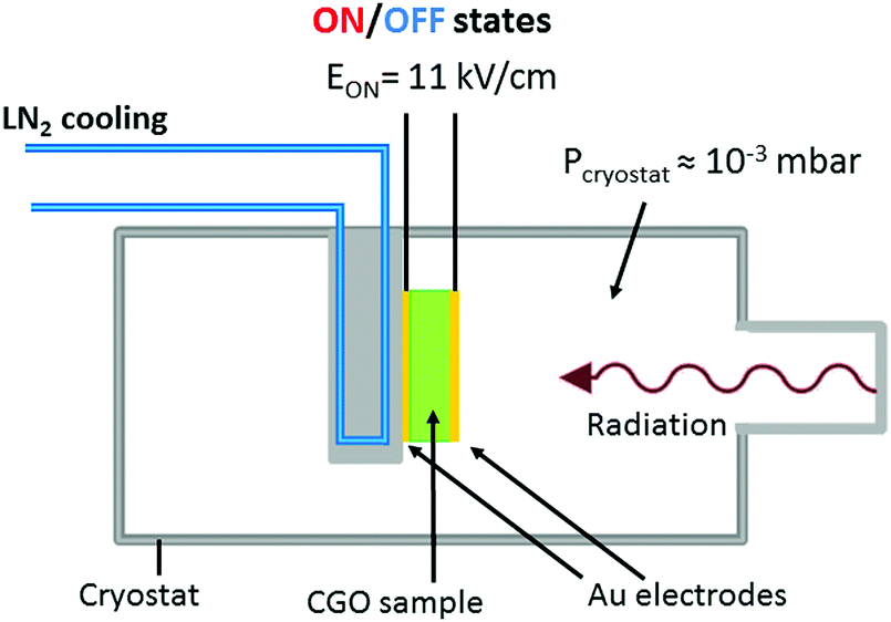 | ||
| Fig. 1 Schematics of the cryogenic chamber adapted to the in situ measurements. | ||
Quantitative analysis of X-ray absorption near edge spectroscopy (XANES) spectra was performed to evaluate the difference in the ON and OFF states. This analysis was done by peak Gaussian arc-tg fitting and area calculation. Extended X-ray absorption fine structure (EXAFS) spectroscopy was performed in both ON and OFF states and then the differential spectra (Δχ(k) = χ(k)on − χ(k)off) were analyzed as described in the Results and the ESI.†
Atomistic simulations
We used Density Functional Theory (DFT) mainly to investigate the effects of strain on the electronic density at the atomistic level. Each simulation was performed using the Perdew–Burke–Ernzerhof (PBE) exchange–correlation functional,32 as implemented in the GPAW code,33,34 in the plane wave mode (cutoff energy of 800 eV). We applied a Hubbard+U correction of 4.5 eV to the d-orbitals of Ce. To correctly reproduce the same oxygen vacancy observed in the experiments, we created a supercell by repeating the unit cell of CeO2 (2 × 1 × 1) and modifying the lattice vectors ((2√2, 2√2, 1),(2√2, −2√2, 1),(1, 1, 1)). We used a Monkhorst pack k-point mesh of (6 × 6 × 6) throughout the calculations. We applied the strain in the [1−1−0] direction, and the cell relaxed in the direction perpendicular to the strain. All atomic positions are fully relaxed until the forces are below 0.01 eV Å−1. We used the Atomistic Simulation Environment (ASE) package to work with the structures.35 We assumed the oxygen vacancies are random, and our calculations did not include Gd explicitly.Results and discussion
A portion of the single-crystal was cut analyzed by EDS, resulting in chemical purity. Other portions were pulverized, and the XRD analysis indicated a cubic pure fluorite crystal structure with a lattice parameter of 5.4179 Å. This value is slightly larger than what is observed in CGO polycrystalline ceramics, probably due to the absence of grain boundaries in the single-crystals.25,36 The ESI† includes XRD measurements of the powdered single-crystal and graphical representation of the Rietveld refinement (Fig. S2, ESI†).The ionic transport at high temperatures was evaluated between 200 and 600 °C, and the activation energy was calculated to be 0.55 eV (Fig. S3, ESI†). This value is lower than that in polycrystalline samples (above 0.9 eV), probably due to the lack of an ionic blocking effect typical of grain boundaries.
Fig. 2 shows the sample electric field-induced strain (in ppm) for voltage frequencies from 0.15 Hz to 100 Hz. At 0.15 Hz, strain saturation and frequency relaxation are visible, as consistent with CGO ceramics.4,14,37,38
 | ||
| Fig. 2 Electromechanical strain of the CGO single crystal at room temperature for different electric field frequencies measured by laser interferometry (Fig. S1, ESI†). The electrostriction coefficients are reported in Table 1. | ||
Table 1 reports the electrostriction coefficient for the corresponding frequency. These values are comparable to the polycrystalline CGO pellets previously reported.4,14,37,38 Previous results indicate that the electrostriction effect is influenced by the blocking factor and vacancy clustering of the grain boundaries.4,38 However, as the single crystal has a continuous lattice, the characterization here reported is not affected by structural variables and so it is ascribed solely to lattice distortions.
| Electric field frequency (Hz) | 0.15 | 3.7 | 11 | 100 |
|---|---|---|---|---|
| M 33 × 10−18 (m2 V−2) | 3.88 | 0.27 | 0.39 | 0.21 |
For the electromechanical effects at the lattice, we merged and normalized near L-III edge spectra (XANES) of Ce for room temperature (RT), −50 °C, −125 °C, and −194 °C. For each temperature, we report both ON and OFF states as well as the ON–OFF differences. We found that the electric field induces significant Ce local environment change, as evidenced by the differences between the ‘ON’ and ‘OFF’ states of the XANES spectra.
Fig. 3 summarises the results. Fig. 3a shows the main features of the Ce L-III edge spectra: the pre-peak, peak A and peak B, each of which represents a different electronic transition. Fig. 3b reports the difference between ON and OFF states of each feature for different temperatures. Table S2 in the ESI† reports the calculated values.
 | ||
| Fig. 3 (a) Schematics of the Ce L-III edge features position and Gaussian fitting: pre-peak feature at 5722 eV in green, Peak A at 5732 eV in light blue, Peak B at 5739 eV in purple. (b) Area of each feature for ON and OFF states at different temperatures. The numerical data are reported in Table S2 (ESI†). | ||
The pre-peak at 5722 eV was measured to decrease when an electric field is applied (Fig. 3b, green). By reducing the temperature, the difference in the areas became more prominent at −194 °C. The pre-peak feature corresponds to the 2p3/2 → 4f transition, as an effect of 4f and 5d orbital hybridization.39,40 Therefore at low temperature, 4f–5d hybridization appears to be blocked by the external electric field, while it seems negligible at room temperature.
Peaks A and B at 5730–5740 eV showed the opposite behaviour (Fig. 3b, light blue and purple): when we applied the electric field, the area of these features increased. Peaks A and B represent the transition 2p3/2 → 5d.6,41 The increment in these features denotes stronger Ce–O bonds and, consequently, a more dominant ionic nature.1,6,7,41 Such an effect proves that the electric field induces a distortion in a Ce cation's vicinity.1,6,7 By decreasing the temperature, difference in the ON and OFF states becomes higher, reaching roughly double the value between RT and −194 °C.
In summary, low temperatures affect the bond properties of Ce in the presence of an electric field. Cryogenic conditions promote crystal distortion and ionic behaviour while hindering the hybridization of 4f–5d orbitals. This effect, in particular, is visible only at low temperatures.
The DFT results in Fig. 4 confirm the finding. The density of states (DOS, Fig. 4a) shows that the distortion of the structure caused by the strain is responsible for shifting to more negative energies of the valence band edge. By more closely investigating the orbitals accountable for this effect, we also note that both O and Ce orbitals contribute to this shift. The DOS change can more easily be observed by plotting the orbitals at the valence band edge (Fig. 4b). Under strain, the orbitals, mostly pointing towards the Ce-ion, i.e. the [010] plane, as indicated by the blue arrow (left panel, 0%), now rotate and align with the Ce–O plane (right panel, 1%).
 | ||
| Fig. 4 (a) Density of states for different strains (projected); the valence band edge shifts to more negative energies with increasing strain due to a distortion of the structure. (b) The orbitals depicted correspond to the band at the valence band edge for the unstrained and 1% strained configuration. Ce atoms are indicated in yellow, O in red and the oxygen vacancy (VO) in pink. The preferred direction of the orbitals is indicated with the blue arrow. | ||
We performed Extended X-ray Absorption Fine Structure (EXAFS) measurements to clarify the structural mechanisms occurring in the electrostriction. As described in the ESI,† we fitted the first coordination shell around Ce (i.e. the nearest-neighbour oxygen atom). We report the results for χ(k)on and χ(k)off as well as the differential spectrum Δχ(k) = χ(k)on − χ(k)off. In particular, Fig. 5a displays the EXAFS fit at RT under the ‘ON’ state. Fig. 5b shows the fitted RT differential Δχ(k) spectrum. The fit for the other temperatures is in the ESI† (Fig. S4). Table S3 (ESI†) contains the fit results for the ON and OFF states of χ(k) absorption spectra. The coordination number (same for all the dataset N = 7.99 ± 0.23), the nearest neighbour bond length (RCe–O), and the bond disorder factor (σ2) are reported. Table 2 also reports the values of N and R for the OFF state.
 | ||
| Fig. 5 (a) EXAFS fit of room temperature ON state spectrum. (b and c) Fits of the room temperature EXAFS differential spectrum Δχ(k) = χ(k)on − χ(k)off. The fits for the other temperatures are in the ESI.† | ||
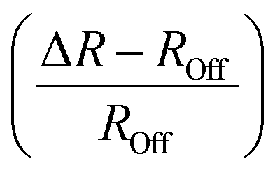 and the fraction (ΔN/NOff) of the electroactive pairs in the lattice at different temperatures. Maximum strain and stress are also reported, considering a constant CGO Young's modulus of 200 GPa1,3
| T (°C) | R OFF | N OFF | ΔR | ΔN | (ΔR − ROFF)/ROFF (%) | ΔN/NOFF (%) | Strain × 10−4 | Stress (MPa) |
|---|---|---|---|---|---|---|---|---|
| 23 | 2.299 | 7.99 | 2.246 | −0.19 | −2.3(2) | 2(1) | 5.5(3.0) | 110(60) |
| −50 | 2.300 | 7.99 | 2.250 | −0.16 | −2.17(3) | 2(2) | 4(5) | 87(110) |
| −125 | 2.301 | 7.99 | 2.040 | −0.33 | −11.3(9) | 4(10) | 46(130) | 937(2600) |
| −194 | 2.304 | 7.99 | 2.219 | −0.99 | −3.689(5) | 12(2) | 45(7) | 914(140) |
As reported in Table S3 (ESI†), we find that the Ce–O bond length is nearly constant with temperature; around 2.30 Å. These results are in general agreement with previous results.6,39,42
The differential analysis between the OFF/ON states allows for analysis of the strain induced by an electric field. The differential spectra Δχ are at different temperatures. Table 2 summarises the differential coordination number (ΔN), and bond length (ΔR) found from the fit. These results are reported in detail in Table S4 (ESI†). The fit coefficients are consistent with the results reported by Lubomirsky et al. for room temperature polycrystalline samples.6 When cooled down, the ΔRCe–O value seems to change with an unclear pattern, suggesting that the magnitude of the electric field-induced distortion is not temperature-dependent.
The coordination number found was negative (ΔN = −0.2 at room temperature), which indicates short Ce–O bonds that are electromechanically active.6,7 Moreover, ΔN decreases from −0.2 at RT to −1 at −194 °C, indicating different bonding dynamics that increase the number of electroactive bonds. The calculated values also indicate that N decreases progressively with the temperature; however, the error bars for −50 and −125 °C are relatively high, and the effect needs further investigation.
We estimate both the fraction of the electroactive bonds and the maximum strain they can develop by comparing the coordination number and Ce–O bond length of the differential and OFF spectra. For instance, at room temperature, the electroactive pairs are about 2% of the total bonds (ΔN/NOff). Additionally, the bond length of these pairs is ∼2.3% shorter (the difference in bond length is (ΔR − ROFF/ROFF)), suggesting that when an electric field is applied, the pairs can generate a maximum distortion on their domain that compensates the 2.3% strain.6 Assuming that all of the pairs contribute equivalently to electrostriction, a strain of 0.055% can form. The assumption suits the single-crystal sample, where pairs have a similar configuration as we do not expect disorder-vacancies interactions.
Table 2 summarises the values calculated for a fraction of electroactive species and the theoretical maximum strain for different temperatures. At −194 °C, the population of electroactive pairs increases to 12%, six times as large as that at room temperature. Therefore, the maximum estimated strain is 4.5 × 10⁻³. Considering that the elastic modulus of CGO is around 200 GPa,1,3 the maximum mechanical stress is estimated to be 110 and 914 MPa at RT and −194 °C, respectively. Unfortunately, a definition of a general trend is problematic due to the significant noise at −50 and −125 °C.
Although direct measurement of the macroscopic strain is missing, our analysis of the crystal shows that the low temperatures favour electrostriction. A primary cause for the effect is the increase in the population of electroactive pairs in the lattice. Reduced vacancy mobility at lower temperatures can induce a stable pair and thus generate local charge anisotropy in the lattice. Another reason can be the cation/anion pair potential's asymmetry, which leads to cell distortion under approximately −150 °C.23
Conclusions
This work reports the electrostrictive properties of a 10 mol% Gd-doped ceria (CGO) single crystal at low temperatures. The sample displayed similar bulk properties to polycrystalline CGO, with frequency relaxation and strain saturation.We performed in situ XAS techniques at the L-III edge of Ce, over a wide temperature range from RT to −194 °C. Analysis of the XANES spectra reveals an increase of the features representing the ionic behaviour of the cerium cations under an intense electric field of ca. 11 kV cm−1 (ON state). The effect increased at lower temperatures.
Differential EXAFS (ON–OFF spectrum) shows an average Ce coordination number (first shell) reduction and shortened Ce–O bond lengths when the electric field is applied. This result indicates an electroactive population that generates local mechanical strain, which changes the shape of the Ce orbitals. Instead of pointing in the [010] direction, the orbitals point along the direction of the Ce–O pair, which we show with DFT calculations. The PDOS analysis also shows that the valence band edge is pushed towards more negative energies for increasing applied strain. We demonstrate that low temperatures significantly increase the number of electrostrictive pairs (by six times from RT to −194 °C). We estimate the maximum expected strain to increase from 5.5 × 10⁻⁴ at RT to 4.5 × 10⁻³ at −194 °C. As the vacancy concentration is constant at low temperatures, this result suggests a heterogeneous population of the pairs with both electromechanically active and inactive configurations in the sample. Such a result in a single-crystal, i.e. with a low degree of crystalline disorder, suggests large-range, electrostatic and elastic interactions, e.g. in the nanometric domain.
Such interactions are temperature-dependent and can affect the pair configuration and, thus, the overall electromechanical properties.
Conflicts of interest
There are no conflicts of interest to declare.Acknowledgements
The Danish Council supported SS for this research by an Independent Research Technology and Production Sciences for the DFF-Research Project 2 (Grant No. 48293). VE and HZ also thank the BioWings project funded by the European Union's Horizon 2020, Future and Emerging Technologies (FET) programme (Grant No. 801267). JKH and VE thank the grant (00022862) from VILLUM FONDEN for partially support this work.References
- R. Korobko, A. Patlolla, A. Kossoy, E. Wachtel, H. L. Tuller, A. I. Frenkel and I. Lubomirsky, Adv. Mater., 2012, 24, 5857–5861 CrossRef CAS PubMed.
- R. Korobko, E. Wachtel and I. Lubomirsky, Sens. Actuators, A, 2013, 201, 73–78 CrossRef CAS.
- S. Santucci, H. Zhang, S. Sanna, N. Pryds and V. Esposito, APL Mater., 2019, 7, 071104 CrossRef.
- A. Kabir, S. Santucci, N. Van Nong, M. Varenik, I. Lubomirsky, R. Nigon, P. Muralt and V. Esposito, Acta Mater., 2019, 174, 53–60 CrossRef CAS.
- M. Hadad, H. Ashraf, G. Mohanty, C. Sandu and P. Muralt, Acta Mater., 2016, 118, 1–7 CrossRef CAS.
- R. Korobko, A. Lerner, Y. Li, E. Wachtel, A. I. Frenkel and I. Lubomirsky, Appl. Phys. Lett., 2015, 106, 042904 CrossRef.
- Y. Li, O. Kraynis, J. Kas, T. C. Weng, D. Sokaras, R. Zacharowicz, I. Lubomirsky and A. I. Frenkel, AIP Adv., 2016, 6, 055320 CrossRef.
- A. Kossoy, A. I. Frenkel, Q. Wang, E. Wachtel and I. Lubomirsky, Adv. Mater., 2010, 22, 1659–1662 CrossRef CAS PubMed.
- A. Kossoy, A. I. Frenkel, Y. Feldman, E. Wachtel, A. Milner and I. Lubomirsky, Solid State Ionics, 2010, 181, 1473–1477 CrossRef CAS.
- V. Esposito and E. Traversa, J. Am. Ceram. Soc., 2008, 91, 1037–1051 CrossRef CAS.
- S. Santucci, H. Zhang, S. Sanna, N. Pryds and V. Esposito, J. Mater. Chem. A, 2020, 8, 14023–14030 RSC.
- V. Sundar and R. E. Newnham, Mater. Res. Bull., 1996, 31, 545–554 CrossRef CAS.
- A. L. Kholkin, C. Wütchrich, D. V. Taylor and N. Setter, Rev. Sci. Instrum., 1996, 67, 1935–1941 CrossRef CAS.
- A. Kabir, H. Zhang, S. Colding-jørgensen, S. Santucci, S. Molin and V. Esposito, Acta Mater., 2020, 187, 183–187 CAS.
- V. Esposito, D. W. Ni, S. Sanna, F. Gualandris and N. Pryds, RSC Adv., 2017, 7, 13784–13788 RSC.
- H. Huang, M. Nakamura, P. Su, R. Fasching, Y. Saito and F. B. Prinz, J. Electrochem. Soc., 2007, 154, 20–24 CrossRef.
- J. L. M. Rupp and L. J. Gauckler, Solid State Ionics, 2006, 177, 2513–2518 CrossRef CAS.
- E. Mishuk, A. D. Ushakov, S. R. Cohen, V. Y. Shur, A. L. Kholkin and I. Lubomirsky, Solid State Ionics, 2018, 327, 47–51 CrossRef CAS.
- A. D. Ushakov, E. Mishuk, E. Makagon, D. O. Alikin, A. A. Esin, I. S. Baturin, A. Tselev, V. Y. Shur, I. Lubomirsky and A. L. Kholkin, Appl. Phys. Lett., 2017, 110, 142902 CrossRef.
- M. V. F. Schlupp, A. Kurlov, J. Hwang, Z. Yung, M. Döbeli, J. Martynczuk, M. Prestat, J. Son and L. J. Gauckler, Fuel Cells, 2013, 13, 658–665 CAS.
- G. Chiodelli, L. Malavasi, V. Massarotti, P. Mustarelli and E. Quartarone, Solid State Ionics, 2005, 176, 1505–1512 CrossRef CAS.
- V. Shelukhin, I. Zon, E. Wachtel, Y. Feldman and I. Lubomirsky, Solid State Ionics, 2012, 211, 12–19 CrossRef CAS.
- A. S. Nowick, Solid State Ionics, 2000, 136–137, 1307–1314 CrossRef CAS.
- J. P. Eufinger, M. Daniels, K. Schmale, S. Berendts, G. Ulbrich, M. Lerch, H. D. Wiemhöfer and J. Janek, Phys. Chem. Chem. Phys., 2014, 16, 25583–25600 RSC.
- K. Michel, J. P. Eufinger, G. Ulbrich, M. Lerch, J. Janek and M. T. Elm, Phys. Chem. Chem. Phys., 2017, 19, 17661–17669 RSC.
- K. Neuhaus, F. Schulze-Küppers, S. Baumann, G. Ulbrich, M. Lerch and H. D. Wiemhöfer, Solid State Ionics, 2016, 288, 325–330 CrossRef CAS.
- S. Berendts and M. Lerch, J. Cryst. Growth, 2011, 336, 106–111 CrossRef CAS.
- L. Simonelli, C. Marini, W. Olszewski, M. Ávila Pérez, N. Ramanan, G. Guilera, V. Cuartero and K. Klementiev, Cogent Phys., 2016, 3(1) DOI:10.1080/23311940.2016.1231987.
- B. Ravel and M. Newville, Phys. Scr., T, 2005, T115, 1007–1010 CrossRef CAS.
- P. J. E. M. Van Der Linden, M. Moretti Sala, C. Henriquet, M. Rossi, K. Ohgushi, F. Fauth, L. Simonelli, C. Marini, E. Fraga, C. Murray, J. Potter and M. Krisch, Rev. Sci. Instrum., 2016, 87, 0–11 CrossRef CAS PubMed.
- C. Marini, R. Boada, J. Prieto Burgos, N. Ramanan, I. García Domínguez, J. Zhao, T. T. Xiao and L. Simonelli, Nucl. Instrum. Methods Phys. Res., Sect. A, 2018, 908, 333–337 CrossRef CAS.
- J. P. Perdew, K. Burke and M. Ernzerhof, Phys. Rev. Lett., 1996, 77, 3865–3868 CrossRef CAS PubMed.
- J. J. Mortensen, L. B. Hansen and K. W. Jacobsen, Phys. Rev. B: Condens. Matter Mater. Phys., 2005, 71, 35109 CrossRef.
- J. Enkovaara, C. Rostgaard, J. J. Mortensen, J. Chen, M. Dułak, L. Ferrighi, J. Gavnholt, C. Glinsvad, V. Haikola, H. A. Hansen, H. H. Kristoffersen, M. Kuisma, A. H. Larsen, L. Lehtovaara, M. Ljungberg, O. Lopez-Acevedo, P. G. Moses, J. Ojanen, T. Olsen, V. Petzold, N. A. Romero, J. Stausholm-Møller, M. Strange, G. A. Tritsaris, M. Vanin, M. Walter, B. Hammer, H. Häkkinen, G. K. H. Madsen, R. M. Nieminen, J. K. Nørskov, M. Puska, T. T. Rantala, J. Schiøtz, K. S. Thygesen and K. W. Jacobsen, J. Phys.: Condens. Matter, 2010, 22, 253202 CrossRef CAS PubMed.
- A. H. Larsen, J. J. Mortensen, J. Blomqvist, I. E. Castelli, R. Christensen, M. Dułak, J. Friis, M. N. Groves, B. Hammer, C. Hargus, E. D. Hermes, P. C. Jennings, P. B. Jensen, J. Kermode, J. R. Kitchin, E. L. Kolsbjerg, J. Kubal, K. Kaasbjerg, S. Lysgaard, J. B. Maronsson, T. Maxson, T. Olsen, L. Pastewka, A. Peterson, C. Rostgaard, J. Schiøtz, O. Schütt, M. Strange, K. S. Thygesen, T. Vegge, L. Vilhelmsen, M. Walter, Z. Zeng and K. W. Jacobsen, J. Phys.: Condens. Matter, 2017, 29, 273002 CrossRef PubMed.
- N. Goykhman, Y. Feldman, E. Wachtel, A. Yoffe and I. Lubomirsky, J. Electroceram., 2014, 33, 180–186 CrossRef CAS.
- A. Kabir, J. R. Bowen, M. Varenik, I. Lubomirsky and V. Esposito, Materialia, 2020, 12, 3–8 CrossRef.
- A. Kabir, J. Kyu Han, B. Merle and V. Esposito, Mater. Lett., 2020, 266, 127490 CrossRef CAS.
- A. M. Shahin, F. Grandjean, G. J. Long and T. P. Schuman, Chem. Mater., 2005, 17, 315–321 CrossRef CAS.
- J. C. Kuang, Adv. Mater. Res., 2014, 1022, 72–75 CAS.
- F. Zhang, P. Wang, J. Koberstein, S. Khalid and S. W. Chan, Surf. Sci., 2004, 563, 74–82 CrossRef CAS.
- T. Ohashi, S. Yamazaki, T. Tokunaga, Y. Arita, T. Matsui, T. Harami and K. Kobayashi, Solid State Ionics, 1998, 113–115, 559–564 CrossRef CAS.
Footnote |
| † Electronic supplementary information (ESI) available. See DOI: 10.1039/d1cp00748c |
| This journal is © the Owner Societies 2021 |