
 Open Access Article
 This Open Access Article is licensed under a Creative Commons Attribution-Non Commercial 3.0 Unported Licence
Transport mechanisms in Co-doped ZnO (ZCO) and H-irradiated ZCO polycrystalline thin films
A.
Di Trolio
 *a,
A.
Amore Bonapasta
b,
C.
Barone
cd,
A.
Leo
c,
G.
Carapella
c,
S.
Pagano
cd,
A.
Polimeni
e and
A. M.
Testa
b
*a,
A.
Amore Bonapasta
b,
C.
Barone
cd,
A.
Leo
c,
G.
Carapella
c,
S.
Pagano
cd,
A.
Polimeni
e and
A. M.
Testa
b
aCNR-Istituto di Struttura della Materia, U.O.S. di Tor Vergata, Via del fosso del cavaliere 100, 00133 Roma, Italy. E-mail: antonio.ditrolio@cnr.it
bCNR-Istituto di Struttura della Materia, Via Salaria Km. 29,300, 00015 Monterotondo St., Roma, Italy
cDipartimento di Fisica “E.R. Caianiello”, Università di Salerno, Via Giovanni Paolo II 132, 84084 Fisciano (SA), Italy
dCNR-SPIN, c/o Università degli Studi di Salerno, 84084 Fisciano (SA), Italy
eDipartimento di Fisica, Sapienza Università di Roma, P.le A. Moro 2, 00185 Roma, Italy
First published on 11th January 2021
Abstract
In the present study, the electrical resistivity (ρ) as a function of the temperature (T) has been measured in polycrystalline ZnO, Co-doped ZnO (ZCO) and H irradiated ZCO (HZCO) samples, in the 300–20 K range. The achieved results show impressive effects of Co doping and H irradiation on the ZnO transport properties. The Co dopant increases the ZnO resistivity at high T (HT), whereas it has an opposite effect at low T (LT). H balances the Co effects by neutralizing the ρ increase at HT and strengthening its decrease at LT. A careful analysis of the ρ data permits to identify two different thermally activated processes as those governing the charge transport in the three materials at HT and LT, respectively. The occurrence of such processes has been fully explained in terms of a previously proposed model based on an acceptor impurity band, induced by the formation of Co-oxygen vacancy complexes, as well as known effects produced by H on the ZnO properties. The same analysis shows that both Co and H reduce the effects of grain boundaries on the transport processes. The high conductivity of HZCO in the whole T-range and its low noise level resulting from electric noise spectroscopy make this material a very interesting one for technological applications.
1. Introduction
In Dilute Magnetic Semiconductors (DMS), a small amount of a magnetic element generates long range ferromagnetic ordering, generally via a carrier-mediated mechanism, that makes DMS important, potential components of spintronic devices.1–3 In the DMS family, Cobalt doped ZnO (ZCO) plays a primary role. In such a material, ZnO properties like large band gap (3.4 eV), long spin coherence length (10.7 nm at 10 K) and large exciton binding energy (60 meV), combine with the occurrence of ferromagnetism (FM) at room temperature (RT).4,5 Interestingly, the ZCO ferromagnetic properties can be improved by increasing the electron density through a co-doping with different ZnO shallow donors.6–12 Among possible shallow donors, atomic H stands out for some peculiar advantages. A mild incorporation of atomic hydrogen in the semiconductor lattice permits indeed an n-type doping of the material by performing post-growth treatments which minimize damaging effects.7 Moreover, in addition to the introduction of shallow donor levels and to the ensuing increase of conductivity,13–16 atomic H can neutralize electron traps at the surface of ZnO grain boundaries (GB)17,18 and it may reduce the O contents by favoring the formation of defects such as oxygen vacancies (VO) and Zn interstitials (Zn-int). VO have been proposed as components of Co-VO complexes playing a key role in the occurrence of RT FM.19,20 Zn-int defects may further increase the n-type carrier density.Many studies have been focused on the ZCO and H+-irradiated ZCO (HZCO) magnetic properties.6–12 However, in view of technological applications, it is also of crucial importance to understand the mechanisms governing charge transport processes in these materials. In this regard, preliminarily, it can be helpful to recall some previous results concerning the effects induced by Co doping and H irradiation on the ZnO properties. ZnO generally shows an n-type character due to shallow-donor native defects or unintentional dopants like, e.g., Zn-int or Al atoms substituting the Zn ones, respectively. As mentioned above, H can significantly increase the ZnO and ZCO conductivity. In the latter material, however, it also gives rise, together with the Co dopants, to somewhat surprising phenomena.7 As a matter of fact, it has been observed that HZCO samples showing a larger ferromagnetic enhancement, directly related to the H dose, show at the same time a lower n-type carrier density, as if Co atoms had a sort of compensating acceptor-effect of the H donors.7 The same acceptor-like behavior is indicated by a reduction of the n-type carrier density observed when Co atoms are introduced in n-type ZnO.20 Both results are quite surprising, a Co-induced compensation of shallow donors seems indeed incompatible with the fact that it is an isoelectronic impurity substituting a Zn atom. In the above cited studies,7,20 a model has been proposed to explain these puzzling findings, founded on the appearance of an acceptor impurity band close to the ZnO conduction band (CB), which originates from electronic states induced by Co-VO complexes.19 This model, further supported by subsequent studies,12,21 will be recalled in the following discussion of present results.
As far as charge transport processes are concerned, many studies were focused on polycrystalline ZnO.22–31 Only few studies addressed the same processes in ZCO27,32 with only two papers devoted to transport mechanisms in hydrogenated ZnO.18,29 No papers have been published on transport processes in HZCO, at the best of the author knowledge. Such a lack of information and the previous results showing that both Co doping and ZCO H co-doping can affect the ZnO conductivity, have motivated the present study of transport properties in polycrystalline PLD (pulsed laser deposition) grown ZnO, ZCO and HZCO thin films, where the electrical resistivity has been investigated from RT down to 20 K.
The achieved results were beyond our expectations by showing that both Co doping and H co-doping produce impressive effects on the ZnO resistivity. More specifically, it is shown that Co doping induces unexpected, opposite effects on the ZnO resistivity in the high temperature (HT) and low temperature (LT) regimes, respectively: it increases the ZnO resistivity in the former case while it induces the reverse in the latter one. On the other hand, H neutralizes the Co-induced increase of resistivity at HT whereas it enhances the resistivity decrease at LT, by realizing a sort of balancing effect, resulting in an overall reduction of the ZnO resistivity in the whole investigated temperature range.
A careful analysis of our results has allowed us to identify two different thermally activated processes playing a primary role in the transport mechanisms at the HT and LT regimes, respectively. The occurrence of such processes has been fully explained on the base of the mentioned model explaining the apparent Co acceptor behavior and on previously observed effects induced by Co doping and H irradiation on the ZnO properties.7,20
The above investigations have been integrated with electric noise spectroscopy measurements of the HZCO sample showing that this material combines the known FM properties, the low resistivity and good mobility with a quite low noise level, thus making this material a very interesting candidate for technological applications.
2. Experimental section
ZnO and 5% Co-doped ZnO films (ZCO), were deposited by pulsed laser deposition using a Nd:YAG laser, operating at λ = 355 nm, with a fluence of 2 J cm−2 and a repetition rate of 10 Hz, and Zn0.95Co0.05O pellets as target. These films were grown on optically transparent Al2O3(001) single crystal substrates, placed at a distance of 5 cm from the target, at 500 °C and 2 × 10⁻⁵ mbar O2 pressure with a growth rate of about 4 Å s−1.7,12,20,21,33–35 The ZCO films were irradiated at 400 °C with a H+ dose of 4.5 × 10¹⁸ ions per cm2 produced by a Kaufman source. Structural and microstructural characterizations, ruling out the presence of noticeable Co-related secondary phases, are reported elsewhere;7,12,20 the thickness, determined by scanning and transmission electron microscope measurements, was (300 ± 30) nm.12 Carrier concentration (n) and mobility (μ) of the ZnO, ZCO and HZCO samples were estimated at RT by Hall measurements.7,20Four-probe dc resistance measurements were carried out by a standard technique with an inline geometry for the contacts, ultrasonically bonded to Al pads defined by optical lithography and lift-off, see Fig. 1. The samples were biased with a Keithley mod. 220 current source and the output voltage was amplified with homemade low-noise electronics and recorded with a Keithley mod. 2002 voltmeter. Resistivity was derived from the R vs. T measurements taking into account film thickness and geometrical factors.
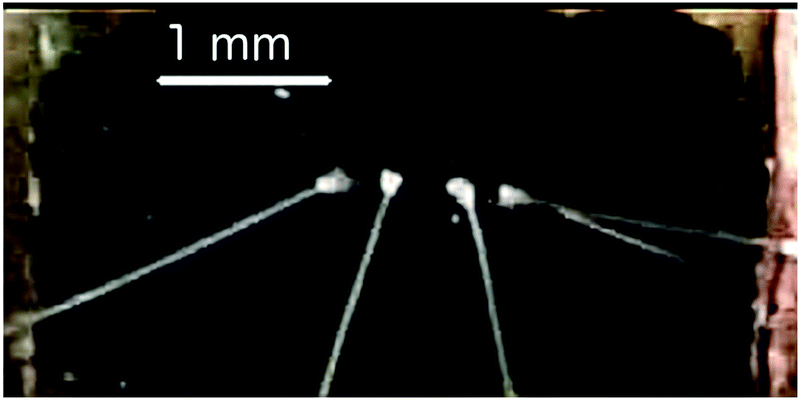 | ||
| Fig. 1 Micro photograph of the sample with the inline bonding pads. Square 150 nm thick Al pads have 200 μm sides and are separated by 200 μm wide gaps. the voltage pads distance is l = 200 μm. The sample width is 5 mm. | ||
A similar configuration of the contact pads was used for temperature and voltage-noise characterizations, made with a closed-cycle refrigerator system (Janis Research) operating in the 8–325 K range with an active temperature stabilization of 0.2 K. The data acquisition was performed using bias and readout electronics optimized for low-noise measurements,36,37 whose effectiveness was already proven in several condensed matter systems.38–40
3. Results and discussion
3.1 Electric transport processes
The measured resistivity (ρ) of ZnO, ZCO and HZCO samples is shown in Fig. 2 as a function of the temperature, T. The curves in the figure exhibit an increase in resistivity with decreasing T, according to a general semiconducting behavior. Most important, the ZnO and ZCO curves show a striking effect of Co doping on the ZnO resistivity. | ||
| Fig. 2 Resistivity (ρ) measurements as a function of temperature for ZnO, ZCO, and HZCO films in the range 20–300 K. | ||
As mentioned above, Co induces indeed opposite effects on the ZnO resistivity by increasing its value in the HT regime and producing the opposite effect in the LT one, respectively. This produces an unexpected crossing of the two curves at an intermediate temperature. Even H has remarkable effects by neutralizing the ρ increase induced by Co doping at HT and strengthening the ρ reduction at LT. Moreover, it also induces the lowest ρ values in the whole sampled T-range, thus avoiding any crossing among the ρ curves.
The shapes of the ρ curves suggest the occurrence of different thermally activated processes.26 In order to get a first information on such processes, our ρ data were fitted in terms of ρ−1 conductivity in the whole temperature range to the following equation:41,42
| ρ−1 = pe−E1/kT + qe−E2/kT + me−E3/kT | (1) |
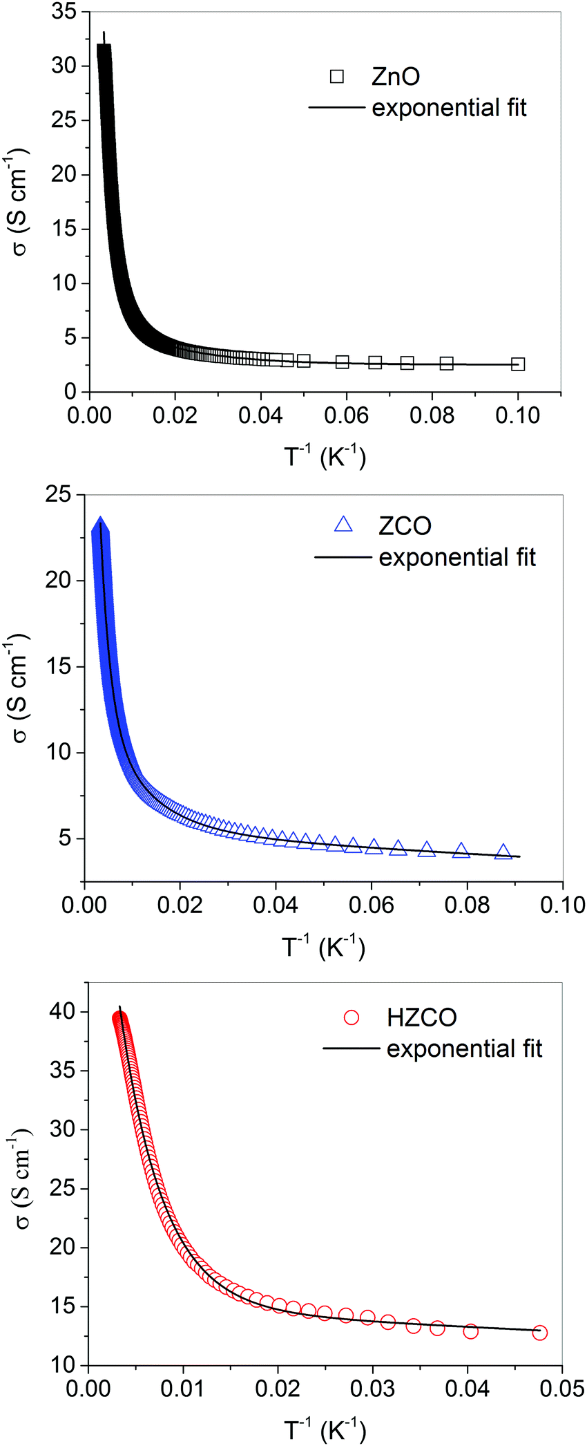 | ||
| Fig. 3 Conductivity (ρ−1) as a function of T−1 for ZnO, ZCO, and HZCO films in the range 20–300 K; solid lines represent a fit to eqn (1) (see text). | ||
| Samples | E 1 (K) (meV) | E 2 (K) (meV) | E 3 (K) (meV) | n (× 1018 cm−3) | μ (cm2 V−1 s−1) | ρ @300 K (Ω cm) | ρ @20 K (Ω cm) |
|---|---|---|---|---|---|---|---|
| ZnO | 417 ± 5 | — | 51 ± 5 | 9.0 ± 0.1 | 7 ± 1 | 0.032 ± 0.001 | 0.350 ± 0.001 |
| 36.0 ± 0.4 | 4.6 ± 0.4 | ||||||
| ZCO | 492 ± 4 | 105 ± 3 | 3.9 ± 0.2 | 2.0 ± 0.1 | 15 ± 1 | 0.043 ± 0.001 | 0.220 ± 0.001 |
| 42 ± 2 | 9.0 ± 0.3 | 0.34 ± 0.01 | |||||
| HZCO | 220 ± 5 | — | 3 ± 1 | 3.4 ± 0.1 | 21 ± 1 | 0.025 ± 0.001 | 0.080 ± 0.001 |
| 19.0 ± 0.4 | 0.25 ± 0.09 |
It turns out that the materials show a different number of thermally activated processes in the investigated T-range. In ZnO, two process are active in the 300–170 K and 170–20 K T ranges, respectively. Three processes occur in ZCO in the 300–240 K, 240–154 K and 154–20 K ranges, respectively, whereas two processes occur in HZCO in the 300–117 K and 117–20 K ranges, respectively. Thus, in order to perform a homogeneous comparison of the three materials, we specify the 300–240 K and the 117–20 K ranges as corresponding to the HT and LT regimes, respectively.
Firstly, the results in Table 1 confirm the significant effect of Co doping on the ZnO conductivity mechanisms, as shown by the appearance of a third thermally activated process, as well as the balancing effect of H that restores the number of thermally activated processes back to two. Then, to identify the kind of thermally activated process which dominates the conductivity mechanisms in the three materials, we have analyzed the above results by distinguishing the HT regime from the LT one. Such an analysis has been performed by taking into account the polycrystalline nature of our samples,7,20 where grain boundaries (GB) could play a significant role in the transport processes. In particular, in the case of ZnO, its surface reactivity and n-type nature, which implies a noticeable presence of electrons in the CB, induce the formation of O2-derived, negatively charged defects at the grain boundary surfaces. Such defects produce a depletion layer of electrons close to the surface and a buildup of negative charge at grain boundaries. This phenomenon gives rise to a band bending in the bulk region near the GB inducing a potential barrier between the grains (Vb) that can inhibit inter-grain electronic transport. By the way, note that the Vb's can be of variable height possibly depending on the surface microstructure (e.g., on the O2-like defect density).
In principle, in polycrystalline materials, the conduction mechanisms can be affected by thermally activated processes which control the intra-grain electron transport (ig processes) or the inter-grain one through the GB barriers (gb processes). In a given T-range, the ig or gb process requiring the largest activation energy is expected to be the “bottle-neck” process that governs the conduction mechanisms.
 | (2) |
If E00 < kT condition is satisfied a TE process is the relevant charge transport mechanism. In the case of our samples, where nZnO = 9 × 1018 cm−3, nZCO = 2 × 1018 cm−3, nHZCO = 3.4 × 1018 cm−3, m* = 0.24, and ε(ZnO) = 8.5,25 the E00 value is larger than kT for ZnO (∼41 meV) and comparable to kT for ZCO and HZCO (24 meV) in the whole 300–240 K range.44 Thus, thermionic emission is not the prevalent process at HT.
The occurrence of TAT processes can be ruled out as well by comparing the ZnO E1 value with the ZCO one and by taking into account the results of a previous KPFM (Kelvin Probe Force Microscopy) study on the effects produced by Co doping on the ZnO surface reactivity and electronic properties.21 Such results show that Co introduction strongly reduces the absorption of negative O2-derived species at the ZnO surface, thus inducing a strong reduction of the Vb barriers. We anticipate that such a Co effect is fully confirmed by the results achieved here at the LT regime, that will be discussed in the following paragraphs. Now, if a TAT process dominated the ZnO conduction mechanisms, a reduction of the Vb height induced by the Co doping would give rise to a reduction of the E1 value on going from the ZnO to the ZCO, contrary to the results of Table 1. This rules TAT processes out in the ZnO and ZCO cases. The same conclusion can be drawn in HZCO. In fact, the above findings imply a minor role of grain boundaries in the ZCO transport processes at HT. The same must hold for HZCO since H passivates the O2-like negative surface defects,17,18 thus further reducing the Vb height. We can conclude that the thermal excitations from the D levels to the CB dominate the transport processes at the HT regime in all of the three materials.
The occurrence of this kind of thermally activated process and the model based on an acceptor-like impurity band induced by Co-VO complexes mentioned above perfectly explain the increase of the E1 values at HT in Table 1 and that of the corresponding ρ values in Fig. 2 when going from ZnO to ZCO. The Co-VO impurity band can subtract indeed electrons from the shallow donor levels, thus producing an increase of the activation energy required for electron excitation to the CB and of the ρ values as well.
The introduction of atomic H in the ZCO sample induces the formation of shallow donor levels which compensate for the effects of the acceptor Co-VO impurity band.7,12 This accounts for a decrease of the activation energy and resistivity values, which result to be both smaller even than the corresponding ZnO values. Thus, atomic H fully neutralizes the effects induced by Co doping on the ZnO transport processes at HT.
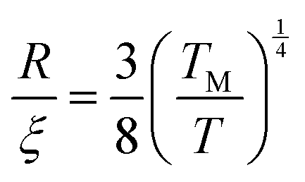
![[thin space (1/6-em)]](https://www.rsc.org/images/entities/char_2009.gif) exp(TM/T)1/4 law, in the range T < 60 K. Fitted values of the characteristic Mott temperature TM are 2400 K, 3164 K, and 2687 K, for the HZCO, ZCO, and ZnO samples, respectively. Two conditions have to be fulfilled for the Mott VRH model to be valid:47
exp(TM/T)1/4 law, in the range T < 60 K. Fitted values of the characteristic Mott temperature TM are 2400 K, 3164 K, and 2687 K, for the HZCO, ZCO, and ZnO samples, respectively. Two conditions have to be fulfilled for the Mott VRH model to be valid:47
(a) the electrons must hop a mean distance R considerably greater than the localization length ξ,48i.e. R/ξ > 1.
(b) the mean hopping energy difference between sites (W) has to be larger than kT, i.e. W/kT > 1.
We calculated such quantities following the Mott relations:
 | (3) |
 | (4) |
exp(TES/T)1/2), with a fitted characteristic temperature TES ∼ 100 K, shows that the conditions for the model validity (R/ξ = (1/4)(TES/T)1/2 > 1 and W/kT = (1/2)(TES/T)1/2 > 1) are once again not fulfilled.47
Therefore, TAT processes dominate the conductivity mechanisms at LT, thus implying a significant GB role. The E3 activation energies estimated indicate that Vb barriers of small amplitude oppose to the charge transport at LT in all the three materials. As anticipated, a ZCO E3 value significantly smaller than the ZnO E3 one fully supports a reduction of the Vb barriers induced by the Co doping. The ZCO E3 activation energy shows a further slight decrease in the case of HZCO. The resulting, overall activation energy trend fully agrees with that of the corresponding ρ values of Fig. 2 at LT. The activation energy and ρ decrease following the Co introduction in ZnO is explained very well by the inhibiting effect of such a doping on the formation of O2-derived defects at the ZnO GB surfaces. On the other hand, the known passivation effects of the same surface defects induced by atomic H17,18 fully account for the further decrease of the HZCO E3 activation energy with respect to the ZCO E3 one. As mentioned above, atomic H introduces also shallow donor levels in the ZnO band structure, which can contribute to a further reduction of ρ values, thus enhancing the effects of Co doping on the ZnO conduction processes at LT.
Altogether, the above considerations give a consistent explanation of the Co doping and H co-doping effects on the ZnO transport properties. Now, it is worth to reconsider the third thermally activated process appearing at an intermediate T for ZCO only. Even in this case, Mott or Efros VRH mechanisms can be ruled out as an origin for that third process. Moreover, we can also rule out processes related to the thermal excitation of electrons from D levels because Co doping cannot induce the formation of donor levels more shallow than those introduced by unintentional dopants or atomic H, as it is indicated by a comparison of the E2 ZCO value with the E1 ZnO and HZCO values in Table 1. Thus, our suspects turn to TAT processes. The occurrence of such a kind of processes seems reasonable since it could be related to a variability of the Vb barriers in ZCO with respect to ZnO and HZCO. In fact, we can assume that at LT these barriers have similar, small heights in ZnO. In ZCO, instead, a variability of the Co concentration in the grains could induce a Vb variability responsible of the appearance of slightly higher barriers which, in turn, would be at the origin of the process requiring slightly higher activation energies (9.0 meV vs. 4.6 meV) at intermediate T. The action of atomic H, given its high diffusion capability, could produce a homogeneous reduction of the ZnO Vb heights, thus restoring the occurrence of only two thermally activated processes at HT and LT, respectively.
We conclude the present section with two final comments. First, the above discussion of LT results indicates a progressive reduction of the GB Vb's on going from ZnO to ZCO, and to HZCO. The same reduction occurs at HT where it is reflected by the RT μ values that significantly increase from ZnO to ZCO and further increase to HZCO, see Table 1. The same table shows that n values lower from ZnO to ZCO. This may indicate that the μ increase due to a reduction of the Vb effects is possibly accompanied by a reduction of electron scattering. On the other hand, n values increase from ZCO and HZCO. In this case, therefore, the μ increase can be exclusively attributed to a Vb reduction. Second, as far as the investigated parameters of Table 1 depend on the Co content, measurements of the carrier density give values of 7.6 × 1018 cm−3, 3.6 × 1018 cm−3, and 2.0 × 1018 cm−3 for ZCO samples 2%, 4%, and 6% Co-doped, respectively. These values, together with the 9.0 × 1018 cm−3n value measured for the ZnO sample, indicate a noticeable decrease of the carrier density for a Co doping level above 4%. This value can be considered, therefore, as a lower bound for Co concentrations able to produce an effective action of the acceptor impurity band. Given the role of such a band in both the HT and LT transport processes, we estimate that the same lower bound similarly affects the μ, ρ, and activation energy values of Table 1. For Co concentrations larger than 6%, the occurrence of a further reduction of the carrier density depends on the Co-VO complex concentration, more specifically on the VO content whose increase may require post-growth treatments.
3.2 Electric noise spectroscopy
In the light of the above results, HZCO can be considered a very interesting material in view of possible opto-spintronics applications due to the coexistence of improved RT magnetic/magneto-optic properties with n-type doping and reduced GB effects and, hence, large electric conductivity and mobility. It is, therefore, useful to investigate its charge carriers fluctuation mechanism, by means of the well-known electric noise spectroscopy. Such technique is based on the study of the voltage fluctuations in the frequency domain, represented by the voltage-spectral density SV, and their dependence on externally controlled parameters such as temperature, bias current, and air pressure.49 Measured SV values of HZCO are shown in Fig. 4a. The measurements were performed in vacuum at RT and in a bias current range varying from 0 to 2 mA and are characterized by a 1/f-type spectrum. At high frequencies, the 1/f noise becomes negligible and SV is dominated by thermal noise, having a white spectrum. The behavior shown in Fig. 4a is expected in the case of films with oriented crystalline structure, as already reported for ZnO samples deposited on glass and Pt/Si substrates,50 for Al-doped ZnO thin films,51,52 and for ZnO-based varistors.53 | ||
| Fig. 4 (a) SV at 300 K for different dc bias current values measured in vacuum. (b) Bias current dependence, measured in vacuum, of the 1/f noise amplitude at 300 and 100 K, showing a quadratic behavior. (c) Measurements of SV at 300 K and at 0.4 mA, in air. | ||
The study of the bias current dependence of the 1/f amplitude has also been performed, since it is a valuable method capable for extracting useful information about the electrical transport mechanisms at work, as extensively reported for a large variety of materials, such as magnetic compounds,54–57 superconducting thin films and devices,58,59 and carbon nanotube composites.60–62Fig. 4b shows a quadratic dependence of the 1/f noise as a function of the bias current, both in the HT (300 K, red squares in Fig. 4b) and in the LT region (100 K, blue dots in Fig. 4b). This behavior, and the decrease of the noise level on lowering the temperature (also evident in Fig. 4b), is typically expected when the noise source is due to resistance fluctuation, according to the Dutta and Horn model,63,64 where the electric transport is explained in terms of thermally activated processes. This result further supports the conduction mechanisms here proposed to explain electric transport in HZCO.
In view of possible applications of HZCO in opto-spintronic devices, noise measurements have been also performed in air and at RT. The SV curves, shown in Fig. 4c, are acquired at the same bias current value of 0.4 mA, and are characterized by a 1/f-type spectrum superimposed to a single small amplitude Lorentzian noise component, having a typical a 1/f2 dependence. We note that the cutoff visible at the highest frequencies is due to finite bandwidth of the electronic readout. The behavior in air differs significantly from the one observed for metal oxide gas sensors,65,66 where high amplitude multi-Lorentzian components in the noise spectra are ascribed to the effect of the adsorbed molecule's density fluctuation on the GB barrier height.67 This is largely different from the noise spectra observed in our case in agreement with the positive role played by H irradiation in decreasing the effect of grain boundaries in polycrystalline Co-doped ZnO thin films.
Moreover, additional information can be obtained from the evaluation of the intrinsic noise level of HZCO, by using the Hooge empirical relation.49 The quantity, [α⋅μ]eff, where α is the Hooge parameter and μ the mobility, is related to the 1/f noise amplitude for unit surface by the equation:49,51
 | (5) |
4. Summary and conclusions
In the present study, the effects of Co doping and of a subsequent H irradiation on the conductivity mechanisms of polycrystalline ZnO thin films have been investigated by measuring the resistivity of ZnO, ZCO and HZCO samples as a function of the temperature in the RT-20 K range. This investigation has produced three major results.First, Co doping has a deep impact on the ZnO transport processes by inducing a resistivity increase at HT, whereas the opposite occurs at low T. This results in a striking crossing of the ZnO and ZCO ρ curves at an intermediate T. Second, the H irradiation rebalances the Co effects by neutralizing the ρ increase at high T and strengthening the ρ decrease at low T. Thus, the combined effect of H and Co doping gives rise to an overall decrease of the ZnO resistivity in the whole sampled T-range.
Third, a careful analysis of the present ρ data has fully clarified the mechanisms governing the charge transport in the three materials by identifying two different thermally activated processes playing a dominant role at HT and LT, respectively. In detail, a thermally activated electron excitation from shallow donor levels to the CB dominates the conduction mechanisms in the three materials in the former regime. On the other hand, a thermally assisted tunneling process governs the charge transport at LT. Grain boundary potential Vb barriers play a primary role in the charge transport only in the LT regime. Remarkably, their effects are reduced by the Co doping with a further reduction by H irradiation of ZCO.
Present results are fully explained in terms of a previously proposed model based on an acceptor impurity band, induced by the formation of Co-VO complexes, as well as reported effects of Co doping21 and H irradiation on the ZnO GB potential Vb barriers.17,18
Finally, electric noise spectroscopy measurements of the HZCO sample, performed in vacuum and air, support the occurrence of thermally activated processes at HT as well as a minor role of GB Vb effects. They also show that the HZCO noise level is significantly lower than that reported in previous papers for ZnO films. Thus, the high conductivity found for HZCO, both in HT and LT regimes, together with its enhanced magneto-optic properties and the excellent noise characteristic, make this material a very interesting candidate for opto-spintronic applications.
Conflicts of interest
There are no conflicts to declare.Acknowledgements
We are grateful to Francesco Cordero for his support to transport measurements. C. B. and S. P gratefully thank University of Salerno for financial support through grants FRB17PAGAN, FRB18CAVAL and FRB19PAGAN.References
- A. Janotti and C. G. Van de Walle, Fundamentals of zinc oxide as a semiconductor, Rep. Prog. Phys., 2009, 72, 126501 CrossRef.
- J. M. D. Coey, M. Venkatesan and C. B. Fitzgerald, Donor impurity band exchange in dilute ferromagnetic oxides, Nat. Mater., 2005, 4, 173 CrossRef CAS.
- J. M. D. Coey, Dilute magnetic oxides, Curr. Opin. Solid State Mater. Sci., 2006, 10, 83 CrossRef CAS.
- Ü. Özgür, Ya. I. Alivov, C. Liu, A. Teke, M. A. Reshchikov, S. Doğan, V. Avrutin, S.-J. Cho and H. Morkoç, A comprehensive review of ZnO materials and devices, J. Appl. Phys., 2005, 98, 041301 CrossRef.
- S. J. Pearton, D. P. Norton, K. Ip, Y. Heo and T. Steiner, Recent Progress in Processing and Properties of ZnO, Prog. Mater. Sci., 2005, 50, 293–340 CrossRef CAS.
- A. J. Behan, A. Mokhtari, H. J. Blythe, D. Score, X.-H. Xu, J. R. Neal, A. M. Fox and G. A. Gehring, Two Magnetic Regimes in Doped ZnO Corresponding to a Dilute Magnetic Semiconductor and a Dilute Magnetic Insulator, Phys. Rev. Lett., 2008, 100, 047206 CrossRef CAS.
- A. Di Trolio, P. Alippi, E. M. Bauer, G. Ciatto, M. H. Chu, G. Varvaro, A. Polimeni, M. Capizzi, M. Valentini, F. Bobba, C. Di Giorgio and A. Amore Bonapasta, Ferromagnetism and conductivity in hydrogen irradiated Co-doped ZnO thin films, ACS Appl. Mater. Interfaces, 2016, 8, 12925 CrossRef CAS.
- H.-J. Lee, C. H. Park, S.-Y. Jeong, K.-J. Yee, C. R. Cho, M.-H. Jung and D. J. Chadi, Hydrogen-Induced Ferromagnetism in ZnCoO, Appl. Phys. Lett., 2006, 88, 062504 CrossRef.
- Y. C. Cho, S.-J. Kim, S. Lee, S. J. Kim, C. R. Cho, H.-H. Nahm, C. H. Park, I. K. Jeong, S. Park, T. E. Hong, S. Kuroda and S.-Y. Jeong, Reversible Ferromagnetic Spin Ordering Governed by Hydrogen in Co-doped ZnO Semiconductor, Appl. Phys. Lett., 2009, 95, 172514 CrossRef.
- Y. C. Cho, S. Lee, H.-H. Nahm, S. J. Kim, C. H. Park, S. J. Lee, S.-K. Kim, C. R. Cho, H. Koinuma and S.-J. Yeong, Conductive and Ferromagnetic Contributions of H in ZnCoO Using H2 Hot Isostatic Pressure, Appl. Phys. Lett., 2012, 100, 112403 CrossRef.
- A. Di Trolio, M. Polichetti, A. Polimeni and A. M. Testa, Local magneto-optical response of H+ irradiated Zn1−xCoxO thin films, Eur. Phys. J.-Spec. Top., 2019, 228(3), 683 CrossRef CAS.
- G. Varvaro, A. Di Trolio, A. Polimeni, A. Gabbani, F. Pineider, C. de Julián Fernández, G. Barucca, P. Mengucci, A. Amore Bonapasta and A. M. Testa, Giant magneto-optical response in H+ irradiated Zn1−xCoxO thin films, J. Mater. Chem. C, 2019, 7, 78–85 RSC.
- C. G. Van de Walle, Hydrogen as a Cause of Doping in Zinc Oxide, Phys. Rev. Lett., 2000, 85, 1012 CrossRef CAS.
- J. J. Dong, X. W. Zhang, J. B. You, P. F. Cai, Z. G. Yin, Q. An, X. B. Ma, P. Jin, Z. G. Wang and P. K. Chu, Effects of Hydrogen Plasma Treatment on the Electrical and Optical Properties of ZnO Films: Identification of Hydrogen Donors in ZnO, ACS Appl. Mater. Interfaces, 2010, 2, 1780 CrossRef CAS.
- W. Chen, L. Zhu, Y. Li, L. Hu, Y. Guo, H. Xu and Z. Ye, Origin of Highly Stable Conductivity of H Plasma Exposed ZnO Films, Phys. Chem. Chem. Phys., 2013, 15, 17763 RSC.
- E. V. Lavrov, J. Weber, F. Borrnert, C. G. Van de Walle and R. Helbig, Hydrogen-related defects in ZnO studied by infrared absorption spectroscopy, Phys. Rev. B: Condens. Matter Mater. Phys., 2002, 66, 165205 CrossRef.
- L. Ding, S. Nicolay, J. Steinhauser, U. Kroll and C. Ballif, Relaxing conductivity/Transparency Trade-Off in MOCVD ZnO Thin Films by Hydrogen Plasma, Adv. Funct. Mater., 2013, 23, 5177 CrossRef CAS.
- D. Gaspar, L. Pereira, K. Gehrke, B. Galler, E. Fortunato and R. Martins, High mobility hydrogenated zinc oxide thin films, Sol. Energy Mater. Sol. Cells, 2017, 163, 255 CrossRef CAS.
- G. Ciatto, A. Di Trolio, E. Fonda, P. Alippi, A. M. Testa and A. Amore, Bonapasta, Evidence of Cobalt-Vacancy Complexes in Zn1−x CoxO Dilute Magnetic Semiconductors, Phys. Rev. Lett., 2011, 107, 127206 CrossRef CAS.
- A. Di Trolio, P. Alippi, G. Ciatto, G. Scavia, M. Valentini and A. Amore Bonapasta, The effect of Co doping on the conductive properties of ferromagnetic Zn1-xCoxO films, J. Mater. Chem. C, 2015, 3, 10188 RSC.
- D. D’Agostino, C. Di Giorgio, F. Bobba, A. Di Trolio, P. Alippi, A. M. Cucolo and A. Amore Bonapasta, Effects of cobalt substitution on ZnO surface reactivity and electronic structure, J. Mater. Chem. C, 2019, 33, 8364 RSC.
- Y.-L. Huang, S.-P. Chiu, Z.-X. Zhu, Z.-Q. Li and J.-J. Lin, Variable-range-hopping conduction processes in oxygen deficient polycrystalline ZnO films, J. Appl. Phys., 2010, 107, 063715 CrossRef.
- C.-C. Lien, C.-Y. Wu, Z.-Q. Li and J.-J. Lin, Electrical conduction processes in ZnO in a wide temperature range 20–500 K, J. Appl. Phys., 2011, 110, 063706 CrossRef.
- A. Tiwari, C. Jin, J. Narayan and M. Park, Electrical transport in ZnO1−δ films: Transition from band-gap insulator to Anderson localized insulator, J. Appl. Phys., 2004, 96, 3827 CrossRef CAS.
- A. P. Roth and D. F. Williams, Properties of zinc oxide films prepared by the oxidation of diethyl zinc, J. Appl. Phys., 1981, 52, 6685 CrossRef CAS.
- A. T. Vai, V. L. Kuznetsov, H. Jain, D. Slocombe, N. Rashidi, M. Pepper and P. P. Edwards, The Transition to the Metallic State in Polycrystalline n-type Doped ZnO Thin Films, Z. Anorg. Allg. Chem., 2014, 640, 1054 CrossRef CAS.
- R. Kumar and N. Khare, Temperature dependence of conduction mechanism of ZnO and Co-doped ZnO thin films, Thin Solid Films, 2008, 516, 1302 CrossRef CAS.
- J. W. Orton and M. J. Powell, The Hall effect in polycrystalline and powdered semiconductors, Rep. Prog. Phys., 1980, 43, 1263 CrossRef.
- A. Singh, S. Chaudhary and D. K. Pandya, Hydrogen incorporation induced metal-semiconductor transition in ZnO:H thin films sputtered at room temperature, Appl. Phys. Lett., 2013, 102, 172106 CrossRef.
- A. K. Das, P. Misra, R. S. Ajimsha, A. Bose, S. C. Joshi, D. M. Phase and L. M. Kukreja, Studies on temperature dependent semiconductor to metal transitions in ZnO thin films sparsely doped with Al, J. Appl. Phys., 2012, 112, 103706 CrossRef.
- Y. Natsume, H. Sakata, T. Hirayama and H. Yanagida, Low-temperature conductivity of ZnO films prepared by chemical vapor deposition, J. Appl. Phys., 1992, 72, 4203 CrossRef CAS.
- L. T. Tseng, A. Suter, Y. R. Wang, F. X. Xiang, P. Bian, X. Ding, A. Tseng, H. L. Hu, H. M. Fan, R. K. Zheng, X. L. Wang, Z. Salman, T. Prokscha, K. Suzuki, R. Liu, S. Li, E. Morenzoni and J. B. Yi1, Intrinsic and spatially nonuniform ferromagnetism in Co-doped ZnO films, Phys. Rev. B, 2017, 96, 104423 CrossRef.
- D. D’Agostino, C. Di Giorgio, A. Di Trolio, A. Guarino, A. M. Cucolo, A. Vecchione and F. Bobba, Piezoelectricity and charge trapping in ZnO and Co-doped ZnO thin films, AIP Adv., 2017, 7, 055010 CrossRef.
- A. Di Trolio, R. Larciprete, S. Turchini and N. Zema, Bulk sensitive x-ray absorption and magnetic circular dichroism investigation of Mn- and Co-doped ZnO thin films, Appl. Phys. Lett., 2010, 97, 052505 CrossRef.
- A. Di Trolio, C. Veroli, A. M. Testa and D. Fiorani, Ferromagnetism above room temperature in Mn-doped ZnO thin films, Superlattices Microstruct., 2009, 46, 101 CrossRef CAS.
- C. Barone, A. Galdi, S. Pagano, O. Quaranta, L. Méchin, J.-M. Routoure and P. Perna, Experimental technique for reducing contact and background noise in voltage spectral density measurements, Rev. Sci. Instrum., 2007, 78, 093905 CrossRef CAS.
- J. M. Routoure, S. Wu, C. Barone, L. Méchin and B. Guillet, A Low-Noise and Quasi-Ideal DC Current Source Dedicated to Four-Probe Low-Frequency Noise Measurements, IEEE Trans. Instrum. Meas., 2020, 69, 194 CAS.
- C. Barone, F. Romeo, S. Pagano, C. Attanasio, G. Carapella, C. Cirillo, A. Galdi, G. Grimaldi, A. Guarino, A. Leo, A. Nigro and P. Sabatino, Nonequilibrium fluctuations as a distinctive feature of weak localization, Sci. Rep., 2015, 5, 10705 CrossRef CAS.
- G. Landi, C. Barone, C. Mauro, A. De Sio, G. Carapella, H. C. Neitzert and S. Pagano, Probing Temperature-Dependent Recombination Kinetics in Polymer: Fullerene Solar Cells by Electric Noise Spectroscopy, Energies, 2017, 10, 1490 CrossRef.
- C. Barone, C. Mauro, A. Sambri, U. Scotti di Uccio and S. Pagano, Conductivity response of amorphous oxide interfaces to pulsed light illumination, Nanotechnology, 2019, 30, 254005 CrossRef CAS.
- S.-P. Chiu, Y.-H. Lin and J.-J. Lin, Electrical conduction mechanisms in natively doped ZnO nanowires, Nanotechnology, 2009, 20, 015203 CrossRef.
- L.-T. Tsai, S.-P. Chiu, J. G. Lu and J.-J. Lin, Electrical conduction mechanisms in natively doped ZnO nanowires (II), Nanotechnology, 2010, 21, 145202 CrossRef.
- C. R. Crowell and V. Rideout, Normalized thermionic-field (T-F) emission in metal-semiconductor (Schottky) barriers, Solid-State Electron., 1969, 12, 89 CrossRef.
- In the case of ZCO, the E00 value has been estimated by taking into account the results of a previous study on Co-doped ZnO nanoparticles (see C. K. Ghosh, K. K. Chattopadhyay and M. K. Mitra, J. Appl. Phys., 2007, 101, 124911 CrossRef ) showing that the ZnO relative dielectric constant ε undergoes a threefold decrease (from 6.1 down to 2.27) for a doping concentration of 2% only. Thus, we have considered that in the case of our 5% Co-doped ZnO, a 40% reduction of ε can be reasonably considered for estimating the E00 parameter.
- N. F. Mott and E. A. Davis, Electronic Processes in Non-Crystalline Materials, Clarendon, Oxford, 2nd edn, 1979 Search PubMed.
- A. L. Efros and B. I. Shklovskii, Coulomb gap and low temperature conductivity of disordered systems, J. Phys. C: Solid State Phys., 1975, 8, L49 CrossRef CAS.
- R. Rosenbaum, Crossover from Mott to Efros-Shklovskii variable-range-hopping conductivity in InxOy films, Phys. Rev. B: Condens. Matter Mater. Phys., 1991, 44, 3599 CrossRef CAS.
- P. W. Anderson, Absence of Diffusion in Certain Random Lattices, Phys. Rev., 1958, 109, 1492 CrossRef CAS.
- S. Kogan, Electronic Noise and Fluctuations in Solids, Cambridge University Press, Cambridge, 1996 Search PubMed.
- G. Leroy, J. Gest, L. Yang and L. K. J. Vandamme, Research on the properties of ZnO films by 1/f noise measurement, 2013 22nd International Conference on Noise and Fluctuations (ICNF), Montpellier, 2013, pp. 1–5 DOI:10.1109/ICNF.2013.6578963.
- A. Barhoumi, G. Leroy, L. Yang, J. Gest, H. Boughzala, B. Duponchel, S. Guermazi and J. C. Carru, Correlations between 1/f noise and thermal treatment of Al-doped ZnO thin films deposited by direct current sputtering, J. Appl. Phys., 2014, 115, 204502 CrossRef.
- A. Achahour, G. Leroy, L. K. J. Vandamme, B. Ayachi, B. Duponchel, N. Waldhoff, K. Blary and J.-P. Vilcot, Suppression of contact noise in a study on 1/f noise as a function of film thickness in Al-doped ZnO, Thin Solid Films, 2018, 645, 70–76 CrossRef CAS.
- L. Z. Hasse, S. Babicz, L. Kaczmarek, J. M. Smulko and V. Sedlakova, Quality assessment of ZnO-based varistors by 1/f noise, Microelectron. Reliab., 2014, 54, 192–199 CrossRef CAS.
- C. Barone, A. Galdi, N. Lampis, L. Maritato, F. Miletto Granozio, S. Pagano, P. Perna, M. Radovic and U. Scotti, di Uccio, Charge density waves enhance the electronic noise of manganites, Phys. Rev. B: Condens. Matter Mater. Phys., 2009, 80, 115128 CrossRef.
- C. Barone, C. Aruta, A. Galdi, P. Orgiani, O. Quaranta, L. Maritato and S. Pagano, Spin-polarized current effects in disordered La0.7Ba0.3MnO3 half-metal thin films, J. Phys. D: Appl. Phys., 2010, 43, 245001 CrossRef.
- M. Asa, C. Autieri, C. Barone, C. Mauro, S. Picozzi, S. Pagano and M. Cantoni, Detecting antiferromagnetism in tetragonal Cr2O3 by electrical measurements, Phys. Rev. B, 2019, 100, 174423 CrossRef CAS.
- C. Cirillo, C. Barone, H. Bradshaw, F. Urban, A. Di Bernardo, C. Mauro, J. W. A. Robinson, S. Pagano and C. Attanasio, Magnetotransport and magnetic properties of amorphous NdNi5 thin films, Sci. Rep., 2020, 10, 13693 CrossRef CAS.
- C. Barone, H. Rotzinger, J. N. Voss, C. Mauro, Y. Schön, A. V. Ustinov and S. Pagano, Current-Resistance Effects Inducing Nonlinear Fluctuation Mechanisms in Granular Aluminum Oxide Nanowires, Nanomaterials, 2020, 10, 524 CrossRef CAS.
- S. Pagano, N. Martucciello, E. Enrico, E. Monticone, K. Iida and C. Barone, Iron-Based Superconducting Nanowires: Electric Transport and Voltage-Noise Properties, Nanomaterials, 2020, 10, 862 CrossRef CAS.
- C. Barone, S. Pagano and H. C. Neitzert, Effect of concentration on low-frequency noise of multiwall carbon nanotubes in high-density polyethylene matrix, Appl. Phys. Lett., 2010, 97, 152107 CrossRef.
- C. Barone, S. Pagano and H. C. Neitzert, Transport and noise spectroscopy of MWCNT/HDPE composites with different nanotube concentrations, J. Appl. Phys., 2011, 110, 113716 CrossRef.
- C. Barone, G. Landi, C. Mauro, H. C. Neitzert and S. Pagano, Universal crossover of the charge carrier fluctuation mechanism in different polymer/carbon nanotubes composites, Appl. Phys. Lett., 2015, 107, 143106 CrossRef.
- P. Dutta and P. M. Horn, Low-frequency fluctuations in solids: 1/f noise, Rev. Mod. Phys., 1981, 53, 497–516 CrossRef CAS.
- C. Barone, H. Rotzinger, C. Mauro, D. Dorer, J. Münzberg, A. V. Ustinov and S. Pagano, Kondo-like transport and magnetic field effect of charge carrier fluctuations in granular aluminum oxide thin films, Sci. Rep., 2018, 8, 13892 CrossRef CAS.
- V. M. Aroutiounian, Z. H. Mkhitaryan, A. A. Shatveryan, F. V. Gasparyan, M. Z. Ghulinyan, L. Pavesi, L. B. Kish and C. Granqvist, Noise spectroscopy of gas sensors, IEEE Sens. J., 2008, 8, 786–790 CAS.
- S. Gomri, T. Contaret and J. Seguin, A New Gases Identifying Method With MOX Gas Sensors Using Noise Spectroscopy, IEEE Sens. J., 2018, 18, 6489–6496 CAS.
- S. Gomri, T. Contaret, J. Seguin, K. Aguir and M. Masmoudi, Modeling in MOX Gas Sensors, Fluct. Noise Lett., 2017, 16, 1750013 CrossRef.
| This journal is © the Owner Societies 2021 |