
 Open Access Article
 This Open Access Article is licensed under a
 Creative Commons Attribution 3.0 Unported Licence
Revealing the electronic structure, heterojunction band offset and alignment of Cu2ZnGeSe4: a combined experimental and computational study towards photovoltaic applications†
Sachin R.
Rondiya
 *a,
Dilara Gokcen
Buldu
bcd,
Guy
Brammertz
bcd,
Yogesh A.
Jadhav
e,
Russell W.
Cross
a,
Hirendra N.
Ghosh
f,
Thomas E.
Davies
a,
Sandesh R.
Jadkar
e,
Nelson Y.
Dzade
*a and
Bart
Vermang
*bcd
*a,
Dilara Gokcen
Buldu
bcd,
Guy
Brammertz
bcd,
Yogesh A.
Jadhav
e,
Russell W.
Cross
a,
Hirendra N.
Ghosh
f,
Thomas E.
Davies
a,
Sandesh R.
Jadkar
e,
Nelson Y.
Dzade
*a and
Bart
Vermang
*bcd
aSchool of Chemistry, Cardiff University, Main Building, Park Place, Cardiff, CF10 3AT, Wales, UK. E-mail: rondiyas@cardiff.ac.uk; dzadeny@cardiff.ac.uk
bInstitute for Material Research (IMO), Hasselt University (Partner in Solliance), Wetenschapspark 1, 3590 Diepenbeek, Belgium. E-mail: bart.vermang@uhasselt.be
cImec division IMOMEC (Partner in Solliance), Wetenschapspark 1, 3590 Diepenbeek, Belgium
dEnergyVille, Thorpark, Poort Genk 8310 & 8320, 3600, Belgium
eSchool of Energy Studies, Savitribai Phule Pune University, Pune 411007, India
fInstitute of Nano Science and Technology, Mohali, Punjab 160062, India
First published on 1st April 2021
Abstract
Cu2ZnGeSe4 (CZGSe) is a promising earth-abundant and non-toxic semiconductor material for large-scale thin-film solar cell applications. Herein, we have employed a joint computational and experimental approach to characterize and assess the structural, optoelectronic, and heterojunction band offset and alignment properties of a CZGSe solar absorber. The CZGSe films were successfully prepared using DC-sputtering and e-beam evaporation systems and confirmed by XRD and Raman spectroscopy analyses. The CZGSe films exhibit a bandgap of 1.35 eV, as estimated from electrochemical cyclic voltammetry (CV) measurements and validated by first-principles density functional theory (DFT) calculations, which predicts a bandgap of 1.38 eV. A fabricated device based on the CZGSe as a light absorber and CdS as a buffer layer yields power conversion efficiency (PCE) of 4.4% with VOC of 0.69 V, FF of 37.15, and Jsc of 17.12 mA cm−2. Therefore, we suggest that interface and band offset engineering represent promising approaches to improve the performance of CZGSe devices by predicting a type-II staggered band alignment with a small conduction band offset of 0.18 eV at the CZGSe/CdS interface.
1. Introduction
In view of the large market size of the energy sector, diversification is crucial for maximizing the potential of PV technologies.1 Cu-based quaternary kesterite semiconductor materials Cu2MSnX4 (M = Zn, Ni, Fe, Co, Cd, and X = S, Se) have attracted significant attention for their possible application in large scale thin-film photovoltaic (PV) technologies because of their tunable direct bandgap (1–1.5 eV), strong optical absorption coefficient (∼104 cm−1), and high carrier mobility (0.1–35 cm2 V−1 S−1) for solar cell applications.2 Despite their germane optoelectronic properties, the kesterite PV device efficiency has stagnated at 12.6%,3 which is significantly lower than the theoretical Shockley–Queisser limit for CZTSSe of 32.8%.4 The lower efficiency of CZTSSe compared to the chalcogenide Cu(In,Ga)(S,Se)2 (CIGS) counterparts (>20% efficiency) has been attributed to several factors, including but not limited to, large open-circuit voltage (Voc) deficits,5–7 high-defect states,8 co-existence of secondary phases,9,10 short carrier lifetime,11 and unfavorable band offset and alignment at the CZTSSe/buffer interface.12,13 In addition to these issues, the kesterite based photovoltaic devices suffer from severe band tailing, which particularly reduces the open circuit voltage (Voc) of solar cells.14 Rey et al. reported the origin of band-tails in kesterite materials and showed that the large band tailing causes voltage losses that limit the efficiency of kesterite-based devices.3,15 However, there have been recent efforts of using single or double cation substitution strategies to control band tailing in CZTS. Yan et al. observed that the introduction of Cd in CZTS can significantly reduce the band tailing issue, which is confirmed by the reduction in the difference between the photoluminescence peak and optical band gap (Eg), as well as a decrease in the Urbach energy.16 Fu et al. reported the suppression of Cu/Zn antisite defects formation via replacement of Zn with Cd, which has a covalent radius ∼18% larger than those of Zn and Cu.17 Lie et al. also observed that the incorporation of Mg in Cu2ZnSnS4 to form Cu2MgxZn1−xSnS4 (varying x from 0.0 to 1.0) could suppress these defects and improve the open circuit voltage.14 Recently, Dhawale et al. reported an improvement in the Voc-deficit mainly due to the reduced band tailing obtained by controlling the Ge/(Sn + Se) ratio.18 Nagaya et al. reported the advantages of Ge in CZTS,19 with a very small tail state formed in CZGSe compared to the large band tailing observed in CZTS and CZTSe. In a previous study, our low-temperature Time-Resolved Photoluminescence (TRPL) Cu2ZnGeSe4 data suggest that a dominant contribution to the observed band tailing in CZT(S,Se) samples comes from the electrostatic potential fluctuations which is totally absent in the Cu2ZnGeSe4 absorber. These efforts have shown positive effects on the current density, grain size, carrier lifetime, and device efficiency. For instance, Kim et al., achieved greater than 10% efficiency with Ge-incorporated Cu2ZnSnSe4 thin-film solar cells.20 In another study, Kim et al., reported improvement of the voltage deficit of Ge-incorporated kesterite solar cell with 12.3% conversion efficiency.21 Collord et al., also reported 11.0% efficient Ge-alloyed kesterite solar cells with low voltage deficits.22However, the thermodynamics and kinetics complexity in the anion, cation, and double cation substitution has resulted in phase instability, complexity of the crystallographic structures, poor band alignment, larger band offsets, uncontrolled compositions, lattice mismatch, irregular grain shapes, and broad size distributions.23 Ge incorporation in kesterite CZTSSe materials along with Sn, widens the bandgap energy from 1.5 to 2.2 eV.24 The widening of the bandgap may be suitable for hydrogen production but limits their application in single-junction solar cells. The Shockley–Queisser limit has given the ideal bandgap 1.34 eV to get record efficiency25 and with non-stoichiometric kesterite-type absorbers, it is possible to achieve an ideal bandgap.26,27
Notwithstanding the several identified beneficial effects in Ge incorporation on CZTSSe absorber properties, further investigations are required to comprehend and optimize this family of materials fully. Pure Ge kesterite (CZGSe), formed by full substitution of Sn by Ge has begun to attract a lot of attention recently as an emerging solar absorber for thin-film solar cells.28 Schnabel et al., reported a power conversion efficiency of 5.1% for a solution based Cu2ZnGeSxSe4−x solar cell with a bandgap of 1.5 eV.29 Sahayaraj et al., reported a power conversion efficiency of 5.5%, with Voc (744 mV), fill factor (46%), and Jsc (16 mA cm−2) for Cu2ZnGeSe4 solar cells with a bandgap of 1.4 eV.30 Choubrac et al., achieved a record efficiency 7.6% for pure Ge kesterite (CZGSe).31 Yang et al., reported numerical modeling of the performance-limiting factors in CZGSe solar cells.32 More recently, Choubrac et al., reported an alternative buffer layer, namely, Zn(O,S,OH) instead of CdS, and achieved 7.5% CZGSe solar cell efficiency.33 Nevertheless, compared to the Sn-based counterparts, several materials properties need to be characterized before further progress can be made in the Ge-based materials. We still require a detailed fundamental understanding of the interface properties like band alignment and band offset at CZGSe/buffer heterojunctions. The band offset is conceivably one of the absorber/buffer interface's essential properties. It dictates the barrier height for the separation and transport of charge carriers across heterojunctions and fabricated devices characteristics.
In the present work, we report the deposition of pure-phase Ge-based kesterite Cu2ZnGeSe4 (CZGSe) thin film and systematically studied its device characteristics, interface band offset, and alignment properties with a CdS buffer layer. PV devices fabricated with these CZGSe thin films exhibited an efficiency of up to 4.4%. Further optimization of the deposition parameters, device fabrication, and band alignments should increase PV efficiency. A staggered type-II band alignment with conduction (0.18 eV) and valence (1.25 eV) band offsets at the CZGSe/CdS interface is determined using Cyclic Voltammetry (CV) measurements and corroborated by our first-principles density functional theory (DFT) calculations. The small conduction band offset (CBO) points to efficient charge separation across the CZGSe/CdS interface.
2. Experimental, characterization, and computational methods
2.1 Deposition of CZGSe thin films and solar cell fabrication
A two-step selenization process was used to deposit the CZGSe thin-films. In the first step, called sequential metal evaporation, the metals were evaporated onto a substrate. A 5 cm2, and 3 mm thick soda lime glass was used as a substrate covered with 120 nm of Si(O,N) and 250 nm of Mo. The two different types of metal layer stacks were deposited on top of this soda lime glass/Si(O,N)/Mo (substrate), one stack with Ge in the bottom of the stack and Cu on top, the other stack with Cu in the bottom and Ge on top. The thicknesses of Ge, Zn, and Cu layers are very important during deposition. The exact layer thicknesses were Ge(180 nm)/Zn(125 nm)/Cu(170 nm) for the stack with Cu on top and Cu(170 nm)/Zn(135 nm)/Ge(200 nm) for the stack with Cu in the bottom. The Pfeiffer PLS 580 electron beam evaporation chamber was used for metal stack evaporation and each layer thickness was controlled with a quartz micro crystal. The prepared films were annealed in the presence of 10% H2Se gas diluted in N2 in an Annealsys AS-150 anneal chamber. We have maintained the ramping step at 1 °C s−1 in the presence of H2Se, followed by 15 min of selenization at a temperature of 460 °C for standard annealing. The CZGSe thin films were cleaned with ammonium sulfide as per our previous report34 and further used to fabricate a PV device with the architecture: glass/Mo/CZGSe/CdS/i-ZnO/Al-ZnO/Ni–Al. A thin n-type CdS layer with 30 nm thickness was deposited via chemical bath deposition on the CZGSe layer.31 An intrinsic ZnO (80 nm) and an aluminum-doped ZnO (400 nm) layer were deposited as transparent conducting oxides using sputtering technique. To improve current collection, a 50 nm of Ni and 1 μm thick Al fingers were deposited as a front contact using a thermal evaporation method. The effective device area of approximately 0.5 cm2 was laterally isolated by mechanical cutting.2.2 Materials characterization
The CZGSe thin films were characterized by various complementary experimental methods. The XRD pattern was obtained with a Bruker D8 Advance X-ray diffractometer using the CuKα line (λ = 1.54 Å) at 1° grazing angle. Phase purity analysis of the CZGSe thin films was done using Renishaw Raman Microscope, applying a wavelength of 532 nm of Nd:YAG laser. The HR-TEM micrographs and selected area electron diffraction (SAED) patterns were obtained with JEOL-JEM 2100 microscope operating at 200 kV. A Kratos Axis Ultra DLD system was used to collect XPS spectra using monochromatic AlKα X-ray source operating at 120 W (10 mA × 12 kV). Data was collected with pass energies of 160 eV for survey spectra, and 20 eV for the high-resolution scans with step sizes of 1 eV and 0.1 eV, respectively. The system was operated in the Hybrid mode of operation which uses a combination of magnetic and electrostatic lenses for electron collection over an analysis area of approximately 300 × 700 μm2. A magnetically confined charge compensation system was used to minimize charging of the sample surface, and all spectra were taken with a 90° take of angle. A pressure of ca. 1 × 10⁻⁹ torr was maintained during collection of the spectra, with base pressure of the system 5 × 10⁻¹⁰ torr. Data was quantified using CasaXPS (v2.3.23) using modified Wagner sensitivity factors as supplied by the manufacturer, after subtraction of a Shirley background. Surface morphology characteristics of the CZGSe thin film were investigated using scanning electron microscopy (JEOL JSM-6360 A). Atomic force microscopy (Bruker Multimode 8.0, Nanoscope AFM in ScanAssyst mode) provided micrographs for the investigation of the surface topology of the thin films. Energy-dispersive X-ray spectroscopy (EDX) measurements were done using Hitachi, S-4800, with EDX spectrum recorded in the binding energy region of 0–10 KeV. The electrochemical cyclic voltammetry (CV) measurements were carried out using Metrohm potentiostat/galvanostat, Autolab PGSTAT 302N (Utrecht, The Netherlands) workstation. A homemade electrochemical cell setup consisting of a commercial Au disk (2 mm diameter) as a working electrode, an Ag wire as a quasi-reference electrode, and Pt wire loop as the counter electrode was used for the CV measurement. Prior to the actual CV measurements, the dilute nitric acid was used to clean the electrodes for 10 min in an ultrasonic bath followed by rinsing in DI water. Controlled CV measurements (blank) were recorded in tetrabutylammonium perchlorate–acetonitrile (TBAP-ACN) mixture. The CZGSe sample dispersion and electrode was prepared as per our earlier report.2,35,36 Typically the working electrode was loaded with CZGSe samples to the cell by drop-casting 200 μL of CZGSe dispersion in 1.0 mg mL−1 ACN followed by vacuum drying. The CV measurements were recorded at a scan rate of 50 mV s−1. The potentials were calibrated with respect to the normal hydrogen electrode (NHE) at the end of each experiment, using ferrocene as an internal standard.35 The fabricated solar cells were analyzed using current–voltage (IV) measurements, and a 2401 Keithley source meter, under standard test conditions for kesterite solar cells with a solar simulator system using an AM1.5 D spectrum with an illumination density of 1000 W m−2 at 25 °C.2.3 Computational methods
To provide an atomic-level insight into the structure and composition of the CZGSe/CdS interface and to understand better the energy band offset and alignment derived from the CV characterizations, we have carried out electronic structure DFT calculations as implemented in the Vienna ab initio simulation package (VASP).37,38 The Perdew–Burke–Ernzerhof (PBE) functional39 was used for structural optimizations, ensuring the residual Hellmann–Feynman forces on all atoms reached 10−3 eV Å−1. The electronic structures were obtained using the screened hybrid functional HSE06 with 25% Hartree–Fock exchange.40 The electronic structures (band structure and projected density of states (DOS)) were calculated using the tetrahedron method.41 The projected augmented wave (PAW) method was used to describe the interactions between the valence and core electrons.38,42 The CZGSe/CdS heterojunction interfaces were constructed with (2 × 2)-CZGSe(001) and a (3 × 2)-CdS(100) supercells, ensuring a lattice mismatch of less than 5%. The Brillouin zone of bulk CZGSe was sampled using the G-centered 5 × 5 × 3 k-mesh with energy kinetic energy cut-off of 600 eV, whereas the constructed interface structures were sampled using 5 × 5 × 1.3. Results and discussions
3.1 Characterization of CZGSe thin film
The XRD pattern of the CZGSe thin film as shown in Fig. 1a, reveals clear, sharp diffraction peaks, confirming the crystalline nature, in good agreement with previous reports.30 The diffraction peaks at 27.71°, 45.76°, 46.15°, 54.35°, and 55.08° correspond to the (112), (220), (204), (312), and (116) crystal planes of the kesterite structure, respectively, and are in good agreement with the International Centre for Diffraction Data (ICDD) reference.30,43 The observed highest peak intensity for the (112) plane indicates that CZGSe prefers growth along (112) direction. Besides the reflections of the CZGSe and Mo, no other peaks were visible in the XRD pattern. Phase confirmation of the CZGSe thin film was done using Raman spectroscopy at room temperature, which yields two major peaks at 175.5 and 204.3 cm−1 (Fig. 1b) in good agreement with previous reports.31 Using first-principles DFT calculations, the structural parameters of kesterite CZGSe (Fig. 1c) were determined. The lattice constants were predicted at a = 5.599 and c = 11.149 Å, which is in good agreement with the experimentally measured ones (a = 5.603 Å and c = 11.045 Å).28 The Cu–Se, Zn–Se, and Ge–Se interatomic bond distances were calculated at 2.389, 2.453, and 2.432 Å, respectively. From the electronic band structure shown in Fig. 1d, a direct bandgap of 1.38 eV is predicted, which is consistent with our estimated electrochemical bandgap and previously reported results based on UV-Vis spectroscopy analyses. It is evident from the total and projected density of states (Fig. 1e) that the valence band maximum (VBM) of CZGSe is composed mainly of Cu-3d and Se-3p states, whereas the conduction band minimum (CBM) is composed primarily of Se-3p states.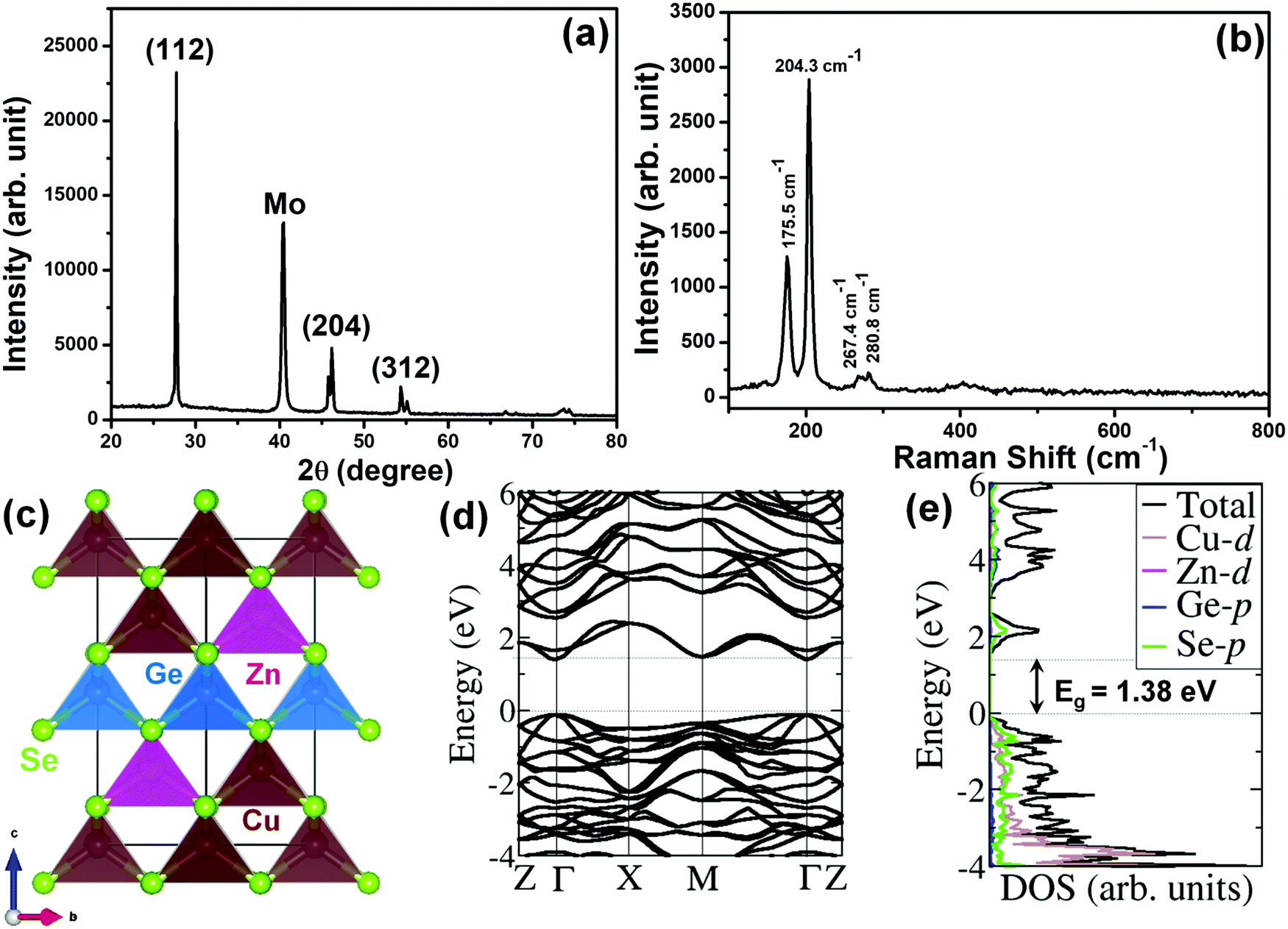 | ||
| Fig. 1 (a) X-ray diffraction pattern and (b) Raman spectroscopy spectra of CZGSe thin film. (c) Crystal structure of kers-CZGSe, and the corresponding (d) the band structure along the high-symmetry directions of the Brillouin zone, (e) ion decomposed partial and total density of states. | ||
The SAED patterns (Fig. 2b) of the area shown in Fig. 2a confirmed the polycrystalline nature of the CZGSe films and of the kesterite structure indexed to ICDD 01-070-7623 as indicated by the diffraction rings corresponding to the (112), (204) and (312) planes. The high-resolution TEM (HR-TEM) image shown in Fig. 2c and the measured lattice planes (Fig. 2d) gives a d-spacing of 0.31 nm, consistent with the d-spacing of the (112) plane of kesterite CZGSe. Energy-dispersive X-ray spectroscopy (EDX) composition analysis (Fig. S1f, ESI†) confirmed the CZGSe films to be Cu-poor and Zn-rich with Cu/(Zn + Ge) and Zn/Ge ratios of 0.87 and 1.18, respectively. The elemental mapping analysis (Fig. S1(a–e), ESI†) by SEM-EDX confirmed an even distribution of the constituent elements. The oxidation states of Cu, Zn, Ge, and Se in the CZGSe thin film were obtained from XPS analysis, as shown in Fig. 3. The binding energy values for Cu 2p3/2 and Cu 2p1/2 are 932.36 and 952.15 eV, respectively, with a peak separation of 19.8 eV. No satellite peaks were found at the higher binding energies, which reveal that only monovalent copper (Cu+) exists in the thin film. The Zn 2p spectra is dominated by 2p3/2 and 2p1/2 located at 1021.95 and 1045.05 eV, respectively, with a separation of 23.1 eV, which can be assigned to Zn(II). Ge(IV) is confirmed by a 3d peak located at 32.23 eV. Selenium(II) is confirmed by the Se 3d5/2 and 3d3/2 peaks located at 54.16 and 54.96 eV, respectively, with a peak splitting 0.80 eV.44 The additional oxide peak at 59.53 eV, corresponds to SeO2.45
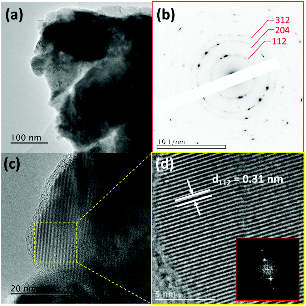 | ||
| Fig. 2 (a) TEM images of CZGSe at 50k×, (b) selected area electron diffraction (SAED) pattern of CZGSe area from (a), (c) HR-TEM image of CZGSe with clear lattice resolution at 400k× showing the amorphous surface layer, (d) zoomed in area shown in (c) with inset power spectrum and lattice spacing of CZGSe indicated. | ||
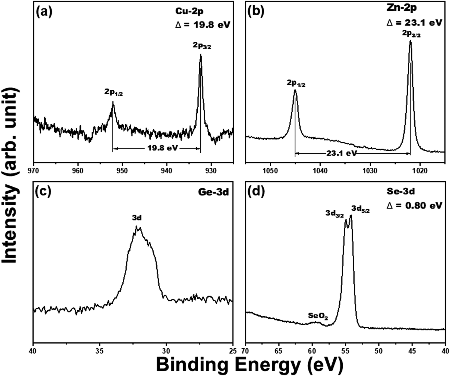 | ||
| Fig. 3 The high-resolution XPS spectra of (a) Cu(2p), (b) Zn(2p), (c) Ge(3d), and (d) Se(3d) core levels of CZGSe thin film. | ||
Scanning electron microscopy (SEM) images of the CZGSe thin film (Fig. S2(a and b), ESI†) show a regular assembly of nanostructures providing a smooth, homogeneous, uniform surface and densely packed micrometer-sized grains. Two-dimensional (2D) and three dimensional (3D) AFM micrographs were taken over 5 μm2 area of CZGSe thin film (Fig. S2(c and d), ESI†), revealing the surface topology of the CZGSe thin films. The 2D AFM micrograph of CZGSe thin film (Fig. S2c, ESI†) indicates that the CZGSe films have a smooth surface with large connected grains, which is very important for carrier transport in solar cells. From the 3D AFM image (Fig. S1d, ESI†), the root mean square roughness (Sm) and average surface roughness (Sa) is found to be 108.12 and 84.40 nm, respectively. The AFM images confirm the formation of uniform and densely packed micrometer-sized grains, which is necessary for heterojunction solar cells.
3.2 CZGSe solar device performance
The CZGSe thin films were used to fabricate a PV cell with an effective device area of 0.5 cm2. A schematic of the device architecture consisting of corning glass/Mo/CZGSe/CdS/i-ZnO/Al–ZnO/Ni–Al is shown in Fig. 4a. The light current density–voltage (J–V) characteristics were measured under AM1.5G illumination density of 1000 W m−2 at 25 °C. The fabricated device exhibits a Voc of 0.69 V, fill factor (FF) of 37.15, a short-circuit current density (Jsc) of 17.12 mA cm−2, and a power conversion efficiency (η) of 4.4% (Fig. 4b). Although the obtained power conversion efficiency is lower than those of recent reports,30,31 but the encouraging structural, optical, compositional, and surface properties suggest that the CZGSe device's efficiency can be improved by optimizing the materials deposition and device fabrication. Optimization of the different layer thicknesses and the CZGSe/CdS heterojunction can reduce interface defect states and improve power conversion efficiency. In thin-film solar cells, the separation and recombination of charge carriers at interfaces provide the basis for converting light into electricity. The efficiency of these processes depends on the quality and perfection of the interface. Device optimization requires a complete understanding of the interface structure and the band offset and alignment at absorber-buffer (CZGSe/CdS) heterojunction. We have employed a combination of cyclic voltammetric (CV) experiments and first-principles methods to determine the band offset and alignment at the CZGSe/CdS heterojunction.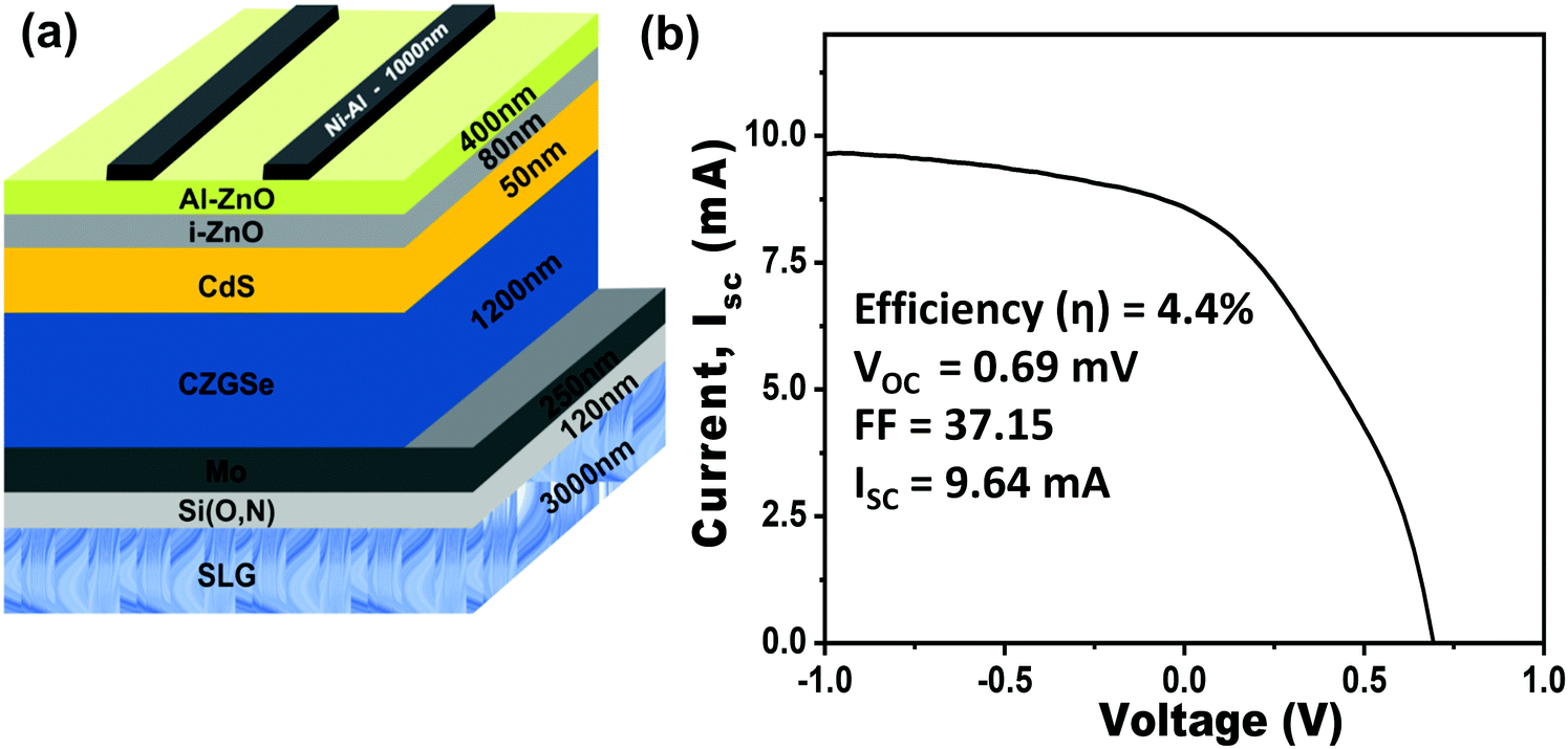 | ||
| Fig. 4 (a) Schematic photovoltaic device fabricated with CZGSe thin films in the glass/Mo/CZGSe/CdS/i-ZnO/Al–ZnO/Ni–Al architecture. (b) Current–voltage characteristics of the fabricated CZGSe PV device, measured under light illumination with 1000 W m−2 intensity. | ||
3.3 Interface structure and band offset
Fig. 5a shows the typical cyclic voltammogram for CZGSe recorded at 50 mV s−1 scan rate. Prominent cathodic (A1) and anodic (C1) peaks at −0.68 V and 0.67 V were noted, which correspond to the oxidation and reduction peaks of CZGSe and can be attributed to the electron transfer from the valence band to conduction band edges, respectively. The separations between the anodic and cathodic peaks in the cyclic voltammogram gives the electrochemical band gap. The detailed description of CV measurements including chemical process is provided in our previous report.46 The electrochemical bandgap, i.e., the potential difference between the peaks, is measured to be 1.35 V, and is in good agreement with our DFT results (1.38 eV) and earlier reported bandgap from the external quantum efficiency (EQE) and the maximum of the PL peak at room temperature (1.36 eV).31 The band edge positions of the CZGSe films are calculated from the oxidation and reduction peaks using the absolute vacuum's standard difference to the potential vs. NHE. The obtained valence and conduction band edge values are −5.17 eV and −3.82 eV, respectively. The estimated values of the bandgap and electron affinity (EA) for CZGSe are 1.35 and 3.82 eV, respectively. Similarly, the bandgap and electron affinity for the n-type CdS is estimated at 2.42 and 4.0 eV, respectively.47 Using the results, we have constructed the band alignment diagram for the CZGSe/CdS heterojunction (Fig. 5b), predicting a staggered type-II band alignment. The conduction band offset (CBO), and valence band offset (CBO) offsets are estimated at 0.18 and 1.25 eV, respectively. The small conduction band offset at the CZGSe/CdS heterojunction promises efficient charge carrier separation and transport, leading to optimal device performance.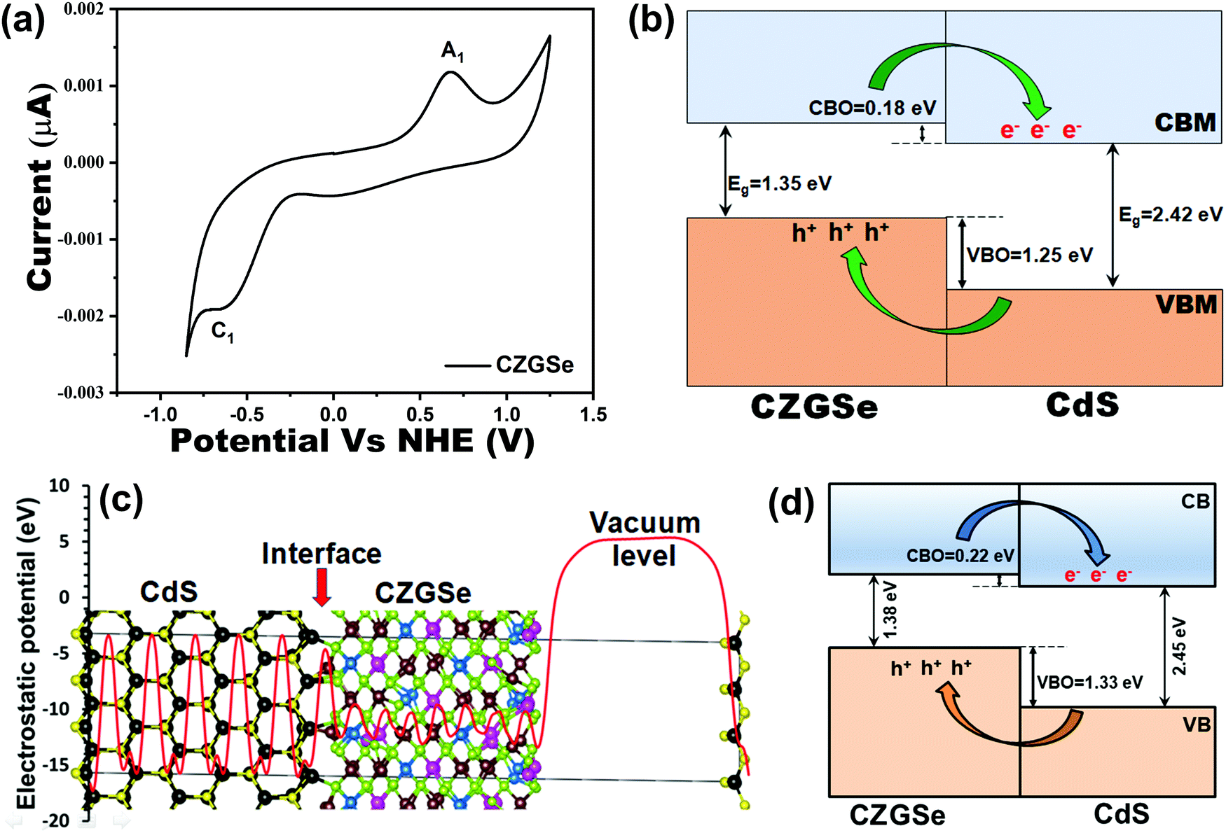 | ||
| Fig. 5 (a) Cyclic voltammogram for CZGSe, which recorded at scan rate of 50 mV s−1. (b) Schematic energy band diagram of p-CZGSe and n-CdS after heterojunction formation in the PV cell, and the carrier collection mechanism at the back- and front contact. Band offsets of 0.18 eV (CBO) and 1.25 eV (VBO) are observed after the CZGSe/CdS heterojunction formation. (c) the geometry optimized model of the CZGSe(001)/CdS(100) interface with the corresponding electrostatic potential, and (d) calculated band alignment at CZGSe(001)/CdS(100) interface. | ||
DFT calculations provided further atomic-level insights into the CZGSe/CdS interface structure, composition, stability, and band offsets. Shown in Fig. 5c is the CZGSe/CdS heterojunction's optimized structure with the corresponding electrostatic potential. The CZGSe/CdS interface is dominated by strong covalent Cu–S (2.255 Å) and Cd–Se (2.782 Å) interactions. The thermodynamic stability of the CZGSe/CdS heterojunction was ascertained by predicting the interfacial adhesion energy (Ead = (ECZGSe/CdS − (ECZGSe + ECdS)/S)), where ECZGSe and ECdS are the total energy of the relaxed CZGSe and CdS slabs, respectively. ECZGSe/CdS is the total energy of the relaxed CZGSe/CdS heterojunction, and S is the surface area of the interface. The adhesion energy for the CZGSe/CdS heterojunction is predicted at −0.187 eV Å−2, indicating a stable interface structure. By applying the potential-line-up method,48,49 the band offsets (BO) at the heterojunction interfaces can be calculated: BO = ΔEV,C + ΔV, where ΔEV and ΔEC is the discontinuity at the VBM and CBM, respectively. ΔV is derived from the line-up of the macroscopic average of the electrostatic potential across the interface. Fig. 5d shows the schematic representation of the band alignment at the CZGSe/CdS interface, predicting a type II staggered band alignment with VBO and CBO values of 1.33 and 0.22 eV, in good agreement with the measured CV data. The higher valence band and conduction band edges of CZGSe than CdS suggest that photo-excited electrons will migrate to the buffer CdS layer and vice versa for holes. These results point to efficient charge separation in the CZGSe/CdS heterojunction, which can be optimized to improve device performance. Consistently, light effective masses of electrons  and holes
 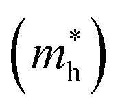 are predicted for CZGSe (Table S1, ESI†) from a fit of the conduction band minimum and valence band maximum energy to a quadratic polynomial in the reciprocal lattice vector k:
 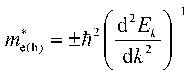 . The electrons have lighter effective masses than the holes, indicating that the electrons are more mobile than the holes, which is expected to promote their efficient separation towards achieving improved solar cell performance.
4. Conclusion
In summary, we report the successful deposition of CZGSe thin films by DC-sputtering and e-beam evaporation and confirmed by XRD and Raman spectroscopy analyses. The CZGSe thin films exhibit a direct bandgap of 1.35–1.38 eV as estimated by electrochemical cyclic voltammetry measurement and validated by first-principles DFT calculations. The fabricated CZGSe solar cell shows a power conversion efficiency of 4.4% with Voc of 0.69 V, FF of 37.15, and Jsc of 17.12 mA cm−2. A staggered type-II band alignment with a small conduction band offset of ∼0.18–0.22 eV is predicted at the CZTS/CdS interface. These results point to efficient separation of photo-excited charge carriers across the CZGSe/CdS interface and suggest that through interface and band offsets engineering, the device efficiency of CZGSe cells can be pushed beyond their current highest efficiency.Conflicts of interest
There are no conflicts to declare.Acknowledgements
SRR and NYD acknowledge the UK Engineering and Physical Sciences Research Council (EPSRC) for funding (Grant No. EP/S001395/1). This work has also used the Advanced Research Computing computational facilities at Cardiff (ARCCA) Division, Cardiff University, and HPC Wales. This work also made use of ARCHER facilities (http://www.archer.ac.uk), the UK's national supercomputing service via the membership of the UK's HEC Materials Chemistry Consortium, which is funded by EPSRC (EP/L000202). YAJ is thankful to Savitribai Phule Pune University Post Doctorate Fellowship (SPPU-PDF) program (Grant No. SPPU PDF/ST/CH/2019/0004) and School of Energy Studies for financial support and laboratory facilities. DGB, GB, and BV acknowledge the European Union's Horizon 2020 Research and Innovation Program (Grant agreement No. 640868). SRR and BV acknowledge UHasselt-BOF for the mobility grant project R-8751 (https://www.uhasselt.be/UH/Research-groups/en-projecten_DOC/en-project_details.html?pid=16044&t=en).References
- A. Wang, N. L. Chang, K. Sun, C. Xue, R. J. Egan, J. Li, C. Yan, J. Huang, H. Rong, C. Ramsden and X. Hao, Sustainable Energy Fuels, 2021, 5, 1044–1058 RSC.
- S. Rondiya, N. Wadnerkar, Y. Jadhav, S. Jadkar, S. Haram and M. Kabir, Chem. Mater., 2017, 29, 3133–3142 CrossRef CAS.
- W. Wang, M. T. Winkler, O. Gunawan, T. Gokmen, T. K. Todorov, Y. Zhu and D. B. Mitzi, Adv. Energy Mater., 2014, 4, 1301465 CrossRef.
- D. B. Mitzi, O. Gunawan, T. K. Todorov, K. Wang and S. Guha, Sol. Energy Mater. Sol. Cells, 2011, 95, 1421–1436 CrossRef CAS.
- B. Shin, O. Gunawan, Y. Zhu, N. A. Bojarczuk, S. J. Chey and S. Guha, Prog. Photovoltaics, 2013, 21, 72–76 CAS.
- S. Tajima, M. Umehara, M. Hasegawa, T. Mise and T. Itoh, Prog. Photovoltaics, 2017, 25, 14–22 CAS.
- D. Shin, B. Saparov and D. B. Mitzi, Adv. Energy Mater., 2017, 7, 1602366 CrossRef.
- T. Gokmen, O. Gunawan, T. K. Todorov and D. B. Mitzi, Appl. Phys. Lett., 2013, 103, 103506 CrossRef.
- X. Zhai, H. Jia, Y. Zhang, Y. Lei, J. Wei, Y. Gao, J. Chu, W. He, J. Yin and Z. Zheng, CrystEngComm, 2014, 16, 6244–6249 RSC.
- S. Siebentritt, Thin Solid Films, 2013, 535, 1–4 CrossRef CAS.
- T. K. Todorov, J. Tang, S. Bag, O. Gunawan, T. Gokmen, Y. Zhu and D. B. Mitzi, Adv. Energy Mater., 2013, 3, 34–38 CrossRef CAS.
- C. Yan, F. Liu, N. Song, B. K. Ng, J. A. Stride, A. Tadich and X. Hao, Appl. Phys. Lett., 2014, 104, 173901 CrossRef.
- S. R. Rondiya, Y. Jadhav, N. Y. Dzade, R. Ahammed, T. Goswami, A. De Sarkar, S. Jadkar, S. Haram and H. N. Ghosh, ACS Appl. Energy Mater., 2020, 3, 5153–5162 CrossRef CAS PubMed.
- S. Lie, S. W. Leow, D. M. Bishop, M. Guc, V. Izquierdo-Roca, O. Gunawan and L. H. Wong, ACS Appl. Mater. Interfaces, 2019, 11, 25824–25832 CrossRef CAS PubMed.
- G. Rey, G. Larramona, S. Bourdais, C. Choné, B. Delatouche, A. Jacob, G. Dennler and S. Siebentritt, Sol. Energy Mater. Sol. Cells, 2018, 179, 142–151 CrossRef CAS.
- C. Yan, K. Sun, J. Huang, S. Johnston, F. Liu, B. P. Veettil, K. Sun, A. Pu, F. Zhou, J. A. Stride, M. A. Green and X. Hao, ACS Energy Lett., 2017, 2, 930–936 CrossRef CAS.
- J. Fu, Q. Tian, Z. Zhou, D. Kou, Y. Meng, W. Zhou and S. Wu, Chem. Mater., 2016, 28, 5821–5828 CrossRef CAS.
- D. S. Dhawale, A. Ali and A. C. Lokhande, Sustainable Energy Fuels, 2019, 3, 1365–1383 RSC.
- K. Nagaya, S. Fujimoto, H. Tampo, S. Kim, M. Nishiwaki, Y. Nishigaki, M. Kato, H. Shibata and H. Fujiwara, Appl. Phys. Lett., 2018, 113, 093901 CrossRef.
- S. Kim, K. M. Kim, H. Tampo, H. Shibata, K. Matsubara and S. Niki, Sol. Energy Mater. Sol. Cells, 2016, 144, 488–492 CrossRef CAS.
- S. Kim, K. M. Kim, H. Tampo, H. Shibata and S. Niki, Appl. Phys. Express, 2016, 9, 102301 CrossRef.
- A. D. Collord and H. W. Hillhouse, Chem. Mater., 2016, 28, 2067–2073 CrossRef CAS.
- M. Ibáñez, R. Zamani, W. Li, A. Shavel, J. Arbiol, J. R. Morante and A. Cabot, Cryst. Growth Des., 2012, 12, 1085–1090 CrossRef.
- G. H. Yue, L. S. Wang, X. Wang, Y. Z. Chen and D. L. Peng, Nanoscale Res. Lett., 2009, 4, 359–363 CrossRef CAS PubMed.
- W. Shockley and H. J. Queisser, J. Appl. Phys., 1961, 32, 510–519 CrossRef CAS.
- A. Ennaoui, M. Lux-steiner, A. Weber, D. Abou-ras, I. Kötschau, H. Schock, R. Schurr, A. Hölzing, S. Jost, R. Hock, T. Voß, J. Schulze and A. Kirbs, Thin Solid Films, 2009, 517, 2511–2514 CrossRef CAS.
- H. Katagiri, K. Jimbo, W. S. Maw, K. Oishi, M. Yamazaki, H. Araki and A. Takeuchi, Thin Solid Films, 2009, 517, 2455–2460 CrossRef CAS.
- L. Shi, P. Yin, H. Zhu and Q. Li, Langmuir, 2013, 29, 8713–8717 CrossRef CAS PubMed.
- T. Schnabel, M. Seboui and E. Ahlswede, RSC Adv., 2017, 7, 26–30 RSC.
- S. Sahayaraj, G. Brammertz, B. Vermang, T. Schnabel, E. Ahlswede, Z. Huang, S. Ranjbar, M. Meuris, J. Vleugels and J. Poortmans, Sol. Energy Mater. Sol. Cells, 2017, 171, 136–141 CrossRef CAS.
- L. Choubrac, G. Brammertz, N. Barreau, L. Arzel, S. Harel, M. Meuris and B. Vermang, Phys. Status Solidi, 2018, 215, 1800043 CrossRef.
- S. Yang, S. Khelifi, G. Brammertz, L. Choubrac, N. Barreau, P. Bolt, B. Vermang and J. Lauwaert, J. Phys. D: Appl. Phys., 2020, 53, 385102 CrossRef CAS.
- L. Choubrac, M. Bär, X. Kozina, R. Félix, R. G. Wilks, G. Brammertz, S. Levcenko, L. Arzel, N. Barreau, S. Harel, M. Meuris and B. Vermang, ACS Appl. Energy Mater., 2020, 3, 5830–5839 CrossRef CAS.
- D. G. Buldu, J. de Wild, T. Kohl, G. Brammertz, G. Birant, M. Meuris, J. Poortmans and B. Vermang, Phys. Status Solidi, 2020, 217, 2000307 CrossRef CAS.
- Y. A. Jadhav, P. R. Thakur and S. K. Haram, Sol. Energy Mater. Sol. Cells, 2016, 155, 273–279 CrossRef CAS.
- S. Rondiya, A. Rokade, P. Sharma, M. Chaudhary, A. Funde, Y. Jadhav, S. Haram, H. Pathan and S. Jadkar, J. Mater. Sci.: Mater. Electron., 2018, 29, 4201–4210 CrossRef CAS.
- G. Kresse and J. Furthmüller, Comput. Mater. Sci., 1996, 6, 15–50 CrossRef CAS.
- G. Kresse and D. Joubert, Phys. Rev. B: Condens. Matter Mater. Phys., 1999, 59, 1758–1775 CrossRef CAS.
- J. P. Perdew, K. Burke and M. Ernzerhof, Phys. Rev. Lett., 1996, 77, 3865–3868 CrossRef CAS PubMed.
- A. V. Krukau, O. A. Vydrov, A. F. Izmaylov and G. E. Scuseria, J. Chem. Phys., 2006, 125, 224106 CrossRef PubMed.
- P. E. Blöchl, O. Jepsen and O. K. Andersen, Phys. Rev. B: Condens. Matter Mater. Phys., 1994, 49, 16223–16233 CrossRef PubMed.
- P. E. Blöchl, Phys. Rev. B: Condens. Matter Mater. Phys., 1994, 50, 17953–17979 CrossRef PubMed.
- G. Brammertz, T. Kohl, J. De Wild, M. Meuris, B. Vermang and J. Poortmans, Thin Solid Films, 2019, 670, 76–79 CrossRef CAS.
- Y. Sun, Y. Zhang, H. Wang, M. Xie, K. Zong, H. Zheng, Y. Shu, J. Liu, H. Yan, M. Zhu and W. Lau, J. Mater. Chem. A, 2013, 1, 6880–6887 RSC.
- B. J. F. Moulder, W. F. Stickle, P. E. Sobol and D. Kenneth, Handbook of XPS_sandeep.pdf, Physical Electronics, 2nd edn, 1992 Search PubMed.
- S. B. Jathar, S. R. Rondiya, Y. A. Jadhav, D. S. Nilegave, R. W. Cross, S. V. Barma, M. P. Nasane, S. A. Gaware, B. R. Bade, S. R. Jadkar, A. M. Funde and N. Y. Dzade, Chem. Mater., 2021, 33, 1983–1993 CrossRef CAS PubMed.
- F. Opoku, K. K. Govender, C. G. C. E. van Sittert and P. P. Govender, Adv. Sustainable Syst., 2017, 1, 1700006 CrossRef.
- A. Alkauskas, P. Broqvist and A. Pasquarello, Phys. Status Solidi, 2011, 248, 775–789 CrossRef CAS.
- C. G. Van de Walle and R. M. Martin, Phys. Rev. B: Condens. Matter Mater. Phys., 1987, 35, 8154–8165 CrossRef CAS PubMed.
Footnote |
| † Electronic supplementary information (ESI) available. See DOI: 10.1039/d0cp06143c |
| This journal is © the Owner Societies 2021 |