Photogenerated carrier dynamics of TIPS-pentacene films as studied by photocurrent and electrically detected magnetic resonance†
Received
29th September 2020
, Accepted 21st December 2020
First published on 23rd December 2020
Abstract
The carrier generation process and spin dynamics through photoexcitation in the vacuum vapour deposition film of 6,13-bis(triisopropylsilylethynyl)pentacene (TIPS-Pn) were investigated by temperature dependence measurements of photocurrent and electrically detected magnetic resonance (EDMR). The EDMR signal was constructed from two components and showed a maximum at approximately 200 K. The temperature dependence was analysed using quantum mechanical simulation, assuming the carrier dynamics of the weakly coupled electron–hole pair (e–h pair). In addition, the analytical formula of photocurrent generation and EDMR signal intensity were also derived based on classical rate equations and used to understand the carrier dynamics. Through phase-shift analysis in quadrature detection of the EDMR signals, one of the two components was well analysed by using a narrow Lorentzian shape, and the other was by using a broad Gaussian.
Introduction
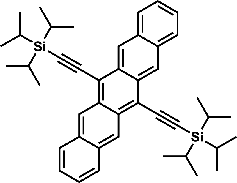
Currently, organic semiconductors have gained attention because they can potentially be fabricated over large areas of flexible substrates at a low cost. Extended π systems such as polyacenes have large intermolecular overlaps due to their π–π stacking in the solid state, leading to high hole mobility. Pentacene is a distinctive example of organic semiconductors, and the carrier mobility of the films has been reported to be 2 cm2 V−1 s−1 and over 50 cm2 V−1 s−1 for single crystals.1,2 Organic semiconductors have attracted increasing attention in the field of spintronics, owing to long-range spin transport properties due to longer spin-relaxation times compared to those of inorganic semiconductors.3,4 Pure spin current was transported in vacuum vapor deposition (VVD) films of TIPS-Pn as well as of pentacene.5 Therefore, pentacene derivatives can be considered as potential candidates for applications in the future organic spintronic devices. However, in applications, pentacene has disadvantages regarding photostability in air and solubility in organic solvents. Significant effort has been made to mitigate these disadvantages such as modification of the electronic structure or insertion of bulky substituents.6,7 Anthony et al. have reported the 6,13-bis(triisopropylsilylethynyl)pentacene (TIPS-Pn; Fig. 1) exhibiting both high photostability and solubility.8,9 We have reported a conceptually different photostabilization approach using pentacene derivatives prepared through the insertion of radical substituents.10,11 In this method, unique excited-state dynamics induced by radical substituents (enhanced intersystem crossing) were utilised to enhance the photostability of the product.12
 |
| | Fig. 1 Molecular structure of TIPS-Pn. | |
Neutral organic semiconductors differ from classical inorganic semiconductors, because the former typically have very few charge carriers (without applying an electrical field) due to negligible natural doping. Although TIPS-Pn and pentacene are representative organic semiconductor materials, detailed studies of their carrier dynamics are still limited. Electron spin resonance (ESR) spectroscopy is particularly suitable for the direct observation of electric-field-induced charge carriers in organic semiconductors. The conventional ESR method successfully clarified the delocalised or mobile nature of the carriers in the pentacene film induced by an applied gate voltage in field-effect transistor (FET) devices.13,14 Electrically detected magnetic resonance (EDMR) was also conducted to clarify the carrier dynamics of pentacene VVD films in a three-layered diode under a specific operating range voltage.15 These studies have focused on the ground-state properties in device applications.
In addition to significant hole mobility, TIPS-Pn and pentacene exhibit photoconductivity under visible-light illumination and persistent photoconductivity within a relatively long lifetime after irradiation.16,17 These materials have also gained increasing attention in singlet fission (SF), in which two triplet-excited states are generated from one photon, exceeding the theoretical Shockley–Queisser limit for power conversion efficiencies.18 SF in pentacene derivative films, including TIPS-Pn, has the potential to lead to high-efficiency photovoltaics. Therefore, photogenerated carrier dynamics in pentacene derivatives represent an important research issue in materials science and photovoltaic device applications. Photocurrent measurements are an important means to study mechanisms such as photogenerated carriers, photoemission, and photoconductance. Although the contribution of the weakly spin-coupled electron–hole (e–h) pair (polaron pair) to the photoelectric-generated carriers has been investigated since the 1960s,19 e–h pairs have recently been attracting attention in organic semiconductor devices such as organic light-emitting diodes20–22 and organic solar cells.23–25 The e–h pairs are generated from excitons and dissociated to charge carriers. The spin dynamics of the e–h pairs have an important role in the photoinduced electron-transfer reaction, leading to photocurrent. Understanding the spin dynamics of the e–h pair is essential to acquiring information on carrier generation and the performance of organic semiconductor devices. EDMR is a powerful method for understanding the spin dynamics (spin-dependent e–h pair generation and recombination mechanisms) in semiconductors. This method detects a microwave-induced current change in the sample caused by the spin dynamics of a weakly spin-coupled e–h pair. In addition, this method is advantageous in terms of sensitivity (compared to the magnetic field-effect measurements of photocurrent) because e–h pairs typically exist only at low concentrations in a device. EDMR has been successfully used to investigate the mechanism of photoconductivity in organic solar cells,23,24 OLEDs,20–22 other polymers,26–28 and low-molecular-weight organics.15,29–31 In this study, the EDMR method will be applied to explain the nature of intermediate e–h pairs possibly involved in the photogeneration of charge carriers in TIPS-Pn. We report the temperature dependence of photocurrent, and photocurrent detected EDMR signals on the VVD films of TIPS-Pn. The temperature dependence was analysed through quantum mechanical simulation along with analytical solutions of conventional rate equations, assuming the carrier dynamics of the weakly coupled e–h pair.
Experimental
VVD films of TIPS-Pn were fabricated on a custom-made interdigitated Pt electrode (Tohnic Inc., substrate: quartz, 125 × 2 digits, digit length: 10 μm, gap: 10 μm, thickness: 150 ± 15 nm Pt with 40 ± 4 nm Ti) using a resistance-heating-type vacuum evaporation apparatus (SVC-700TM/700-2, Sanyu Electron). Ground TIPS-Pn crystals (≥99%, HPLC grade, Sigma-Aldrich Japan) were used as starting materials for VVD without further purification. UV-visible spectroscopy was conducted for steady-state absorption in the CH2Cl2 solution, and the transmission spectrum of the film was obtained using a spectrometer (UV/Vis/NIR, Shimadzu UV-3600). UV-vis diffuse reflectance spectra of the ground powder sample were obtained using a spectrophotometer (Hitachi U-3500). CV measurement was carried out in a CH2Cl2 solution using a multipurpose electrochemical apparatus (Hokuto Dennko HSV-100) under Ar. Tetra-n-butylammonium hexafluorophosphate (TBAPF6) purchased from Sigma-Aldrich (≥97%, NT grade) was purified by recrystallisation and used as the supporting electrolyte (ca. 0.1 M). The photocurrent was detected using a picoammeter (Keithley voltage source 6487) under a voltage bias by light illumination from a Xe lamp (USHIO, UI-501C) followed by a 5 cm pass-length water filter and a UV-vis liquid optical light guide. Excitation light was irradiated from the rear side of the substrate with a platinum electrode and the VVD film, in order to make the influence of the thickness of the film to be inconsequential. The photocurrent-monitored EDMR measurements were carried out at 1.5 V applied bias (MATSUSADA Voltage source, P4K-36) using an X-band ESR spectrometer (JEOL, JES-TE300). The microwave amplitude was modulated with a PIN modulator connected to an arbitrary function generator (TEXIO, AFG-2012). Continuous light illumination was achieved using the same light source setup as in the photocurrent measurements. The photocurrent change induced by microwave amplitude modulation was detected as the voltage change through a custom-made operational-amplifier interface circuit by a lock-in amplifier (Signal Recovery, model 7280). Direct detection of the photocurrent change induced by microwave irradiation (without the amplitude modulation) was also performed using a picoammeter. All instruments for the photocurrent and EDMR measurements were computer controlled using a LabVIEW-based programme made in our laboratory. The sample temperature in the photocurrent and EDMR measurements was controlled by a cooled N2 gas flow system (Oxford ESR900 Cryostat and Oxford, Mercury iTC). An atomic force microscope (AFM; Seiko Instruments Inc., SPI3800N) was used to characterize the morphology of the TIPS-Pn VVD film.
Results and discussion
(i) Optical spectra
The UV-vis optical density spectra of TIPS-Pn are shown in Fig. 2. The solution absorption spectra exhibited a strong peak at 650 nm due to the fundamental ππ* transition, which was identical to that reported previously.9 In both the film and ground powder of TIPS-Pn, the spectral shoulder shifted to ∼700 nm, which can be attributed to π–π stacking;32,33 these two spectra were similar. Therefore, according to the literature, this VVD film is a polycrystalline (and not amorphous) film. The microcrystalline character of the film is consistent with the observations by AFM (see the morphology and AFM photograph in the ESI†).
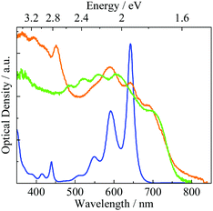 |
| | Fig. 2 UV-vis optical density spectrum of TIPS-Pn absorption in CH2Cl2 solution (blue curve), transmission spectrum of the TIPS-Pn film (orange curve), and diffuse reflectance spectrum of ground powder of the TIPS-Pn sample (green curve). | |
(ii) Photocurrent behaviours
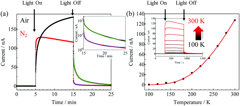
Fig. 3a shows the typical photocurrent behaviour of the TIPS-Pn VVD film at room temperature. Large light-induced conductivity during light illumination was observed both in air and under a N2 atmosphere. In contrast, persistent photocurrent with long lifetimes after radiation was clearly observed under air and a relatively smaller one was also detected under a N2 atmosphere. Similar persistent photocurrent behaviours were reported for the TIPS-Pn transistor,16,17 which was decomposed into two components. The persistent photocurrent decay shown in Fig. 3a was fitted to a biexponential function, as follows:| | 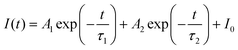 | (1) |
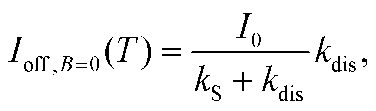
where τ1 and τ2 are the decay-time constants. The lifetimes of each component were determined as τ1 = 12 s (50%) and τ2 = 132 s (50%) under air, and τ1 = 6.1 s (68%) and τ2 = 120 s (32%) under N2 by least-squares fitting using eqn (1) for the current values after turning off the photo-irradiation (light off in Fig. 3a). The percentage of the τ1 and τ2 components in the brackets was estimated by A1/(A1 + A2) and A2/(A1 + A2) using the amplitudes of their components, respectively. These results demonstrated the existence of multi-trap states in the system. To explain the origin of the persistent photocurrent in TIPS-Pn, two mechanisms have been proposed in the literature. One was related to two specific defects that existed at the interface between the dielectric and organic semiconductor phases in a FET device.16 The other was related to degradation due to ambient O2 incorporation.17 Although significant persistent photocurrents were observed in air, little persistent photocurrent behaviour was observed under the N2 atmosphere (Fig. 3a), which indicated that the origin of the persistent photocurrent is observed in the latter. According to the first-principles calculation of unsubstituted pentacene crystals, it is known that the oxygen-bridged pentacene skeleton forms a trap level between the conduction and valence bands.34 In TIPS-Pn, the trap levels are also likely to be formed by the incorporation of oxygen. This trap level could be the origin of the persistent photocurrent. In transition metal heterostructures (MoS2–WS2 multi-junctions), it is recently reported that the distribution of the persistent photoconductivity was clarified using the photoconductive mapping technique, and the persistent photoconductivity was dominated by contributions from the multilayer domains.35 Therefore, the photoconductive mapping technique will give more detailed information of persistent photocurrent in TIPS-Pn VVD films. Fig. 3b shows the temperature dependence of the photocurrent intensity under the N2 atmosphere. In these photocurrent measurements, the external magnetic field (B) and microwaves were not applied; therefore, the field-induced intersystem crossing (S–T0 mixing) originating from the Δg mechanism can be neglected (kISC = 0 s−1 and kESR = 0 s−1). The behaviour of the temperature dependence was well fitted by the analytical solution based on Scheme 1 (see the next section) and eqn (S14) (ESI†) for the photocurrent (Ioff and kESR = kISC = 0 s−1), which is given by:| | 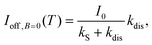 | (2) |
where| | kdis = k0![[thin space (1/6-em)]](https://www.rsc.org/images/entities/char_2009.gif) exp(−E/kBT). exp(−E/kBT). | (3) |
Here, we have introduced the activation energy, E/kB, required to generate carriers from the e–h pair because the photocurrent decreased with the decreasing temperature, as shown in Fig. 3b. The activation energy, E/kB, was determined to be 1103 ± 149 K by least-squares fitting. kS and k0 could not be determined from this fitting because they are temperature interdependent parameters.
 |
| | Fig. 3 (a) Photocurrent and persistent photocurrent responses of the TIPS-Pn film for light illumination using the Xe lamp in air (black curve) and under a N2 atmosphere (red curve) at room temperature. Inset is the decay of the persistent photocurrent depicted using a log scale for the vertical axis. (b) Temperature dependence of the photocurrent response under a N2 atmosphere. | |
 |
| | Scheme 1 Excited-state dynamics and carrier generation process in the VVD film of TIPS-Pn. | |
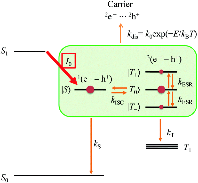
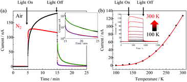
(iii) Model of the carrier generation
The carrier generation model is illustrated in Scheme 1. In this scheme, we have assumed the immediate generation of an e–h pair. The free energy of the e–h pair generation by photoexcitation was roughly estimated using the Rehm–Weller equation.36| | | ΔG = E(D/D+) − E(A−/A) − e2/εε0r − ΔE00 | (4) |
The first and second terms are the oxidation and reduction potential of TIPS-Pn. e2/εε0r is the electrostatic interaction energy of the e–h pair and ΔE00 is the singlet excited-state energy (the 0–0 band excitation energy of TIPS-Pn). The redox potential of TIPS-Pn was determined to be 0.402 V and −1.45 V vs. Fc/Fc+ from cyclic voltammetry in CH2Cl2 solution. We have used these values for a rough estimation of E(D/D+) − E(A−/A) because the corresponding value in the VVD film was not known. The dielectric constant of TIPS-Pn (solid) is reported to be ε = 12.5 at room temperature.37 The intermolecular distance was r = 7.75 Å, as determined by X-ray crystallography analysis.8 The excited singlet energy for TIPS-Pn in the solid state was estimated to be 1.79 eV (691 nm) from the transmission spectrum of the TIPS-Pn film in Fig. 2 (consistent to 1.71 eV from the literature38) and triplet energy has been reported to be 0.87 eV from the literature.38 Using these values, the free energy for the generation of singlet e–h pairs, 1(e–h), from the singlet state was estimated to be negative (ΔG = −0.086 eV). Therefore, their generation is expected to occur spontaneously. In this process, according to the spin selection rule, only 1(e–h) is populated (Scheme 1). SF in the films of TIPS-Pn had been reported;39,40 therefore, rapid spin-allowed generation of the excited triplet state was assumed possible in our system, leading to photocurrent generation from the excited triplet state. However, in contrast to the singlet e–h pair, the free energy of triplet e–h pair generation,3(e–h), from the triplet state, was estimated to be positive (ΔG = 0.728 eV). Thus, triplet e–h pair generation did not occur spontaneously even in the thermal activation of the T1 state of the TIPS-Pn, which was higher than room temperature. The population of the 3(e–h) pairs (ne–h) to that of the T1 state (nT) is expected to be only about ne–h/nT = 10−12 under the thermal equilibrium conditions. In addition, when the contribution from the T1 state in the carrier generation process is dominant, the activation energy (E/kB) for the carrier generation should be larger than ca. 8000 K, which is in contradiction with the results shown latter. Therefore, the initial polarisation in the e–h pair should occur in 1(e–h), as shown in Scheme 1, which is called “S0 born process”.
(iv) Results of EDMR
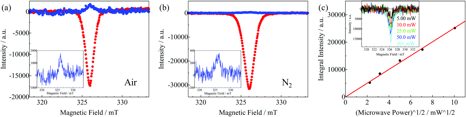
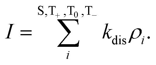
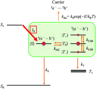
Fig. 4a presents the EDMR spectra of TIPS-Pn obtained by monitoring the photocurrent and the persistent photocurrent at room temperature under air. The opposite sign of the EDMR signals was detected in the g ∼ 2.00 region. Signals of the EDMR of the photocurrent (photocurrent-detected EDMR) correspond to the decrease in the photocurrent (inset of Fig. 5a). Because the same settings of the lock-in amplifier were used in both the EDMR signals of the photocurrent and the persistent photocurrent, the EDMR signals of persistent photocurrent (persistent-current-detected EDMR) probably corresponded to the increase in the persistent photocurrent. Under a N2 atmosphere, the persistent photocurrent was almost negligible, and the photocurrent-detected EDMR signal was similar to that under an air atmosphere.
 |
| | Fig. 4 EDMR spectra of TIPS-Pn through monitoring of the photocurrent (red curve) and the persistent photocurrent (blue curve) at room temperature under (a) air and (b) N2 atmosphere. (c) Photocurrent-detected EDMR spectra of the VVD-prepared TIPS-Pn film as a function of microwave power at 80 K under the N2 atmosphere. | |
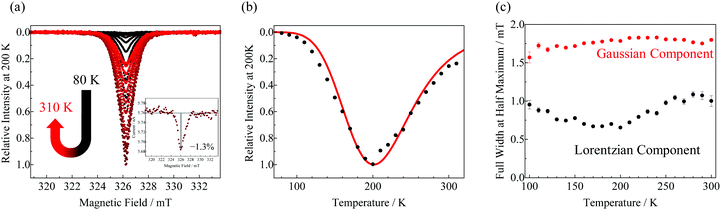 |
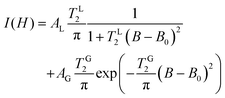
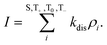
| | Fig. 5 (a) Temperature dependence of the photocurrent-detected EDMR spectra of the VVD film of TIPS-Pn under the N2 atmosphere. (b) Temperature dependence of the integral signal intensity (black dots) and the simulation curve using eqn (S52) (ESI†) (red curve). (c) Temperature dependence of linewidth for Gaussian component to Lorentzian one. The brack circles and red circles show Lorentz and Gaussian analysed by eqn (5). | |
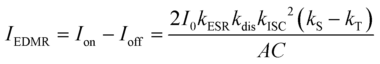
To obtain information regarding the photocarrier-generation process, the microwave power dependence was evaluated, plotting the EDMR spectral intensity versus the square root of the applied power (Fig. 4c). The inset of Fig. 4c shows the observed microwave power dependence of the photocurrent-detected EDMR spectra at 80 K. The spectral intensities were calculated by integrating the area of the EDMR spectra. It should be noted that the signal intensity in a solid is usually saturated at low temperatures, when strong microwave power is applied. This is because of the slow spin–lattice relaxation time. The linear behaviour shown in Fig. 4c indicates that saturation did not occur under the testing conditions, which may derive that the excited-state lifetime of the species in the TIPS-Pn film was sufficiently short. The lower limit of the lifetime (the upper limit of the rate constant) can be estimated from the linewidth of the spectra (ESI†) when the lifetime is much smaller than the spin–spin and spin–lattice relaxation times and the signal line shape is Lorentzian (negligible inhomogeneous broadening). Thus, the upper limit of the rate constant (kS + kdis or kT + kdis in Scheme 1) of the e–h pair was estimated from the linewidth to be 1/τ = 8.6 × 10⁷ s−1 (τ = 1.16 × 10⁻⁸ s).
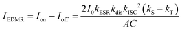
Fig. 5 shows the temperature dependence of the photocurrent-detected EDMR spectra and spectral intensities. The inset of Fig. 5a illustrates the direct detection of the EDMR response for the photocurrent at 200 K using a picoammeter (photocurrent vs. external magnetic field plot at microwave irradiation of 101 mW). The photocurrent decreased by approximately 1.3% under ESR conditions. Thus, the absolute sign of the photocurrent-detected EDMR signal was determined to be negative (decrease) for the photocurrent. As shown in Fig. 5b, the absolute value of the spectral intensity of the EDMR signal increased from 80 to 200 K and then decreased from 200 to 310 K. The spectra were analysed by the superposition of Lorentzian and Gaussian components (eqn (5)). To decrease the variable parameters, we used common g-values (centre field, B0) for the Lorentzian and Gaussian functions.
| |  | (5) |
We confirmed that the EDMR spectra were composed of a narrow Lorentzian and a broader Gaussian line-shape function.
Fig. 5c shows the temperature dependence of the linewidth of each component from 100 to 310 K. Fitting at temperatures below 100 K was difficult because of the poor signal-to-noise ratio. The linewidth of the Gaussian component was independent of the temperature (approximately 1.8 mT). In contrast, the linewidth of the Lorentzian component depended on the temperature, which varied from 0.6 to 1.1 mT. At temperatures below 200 K, the linewidth gradually narrowed with increasing temperatures. This behaviour can be reasonably interpreted by the motional narrowing due to the thermal activation of charge carriers. Temperatures over 200 K led to an increase in the Lorentzian linewidth with increasing temperature owing to shortening in the spin–lattice relaxation time. Similar temperature-dependent linewidth behaviour was also reported in field-induced ESR studies of several OFETs.
14,41
The characteristic behaviours of the observed photocurrent-detected EDMR signals were consistent with the model presented in Scheme 1 (used in the analysis of the characteristic behaviour of the photocurrent). According to this model, the photocurrent (I) is given as the sum of the density (ρ) of each spin sublevel multiplied by the rate constant of the dissociation of e–h pairs (kdis).
| |  | (6) |
It should be noted that in the EDMR experiments the field-induced intersystem crossing (S−T
0 mixing) caused by the Δ
g mechanism occurred (
kISC ≠ 0 s
−1) and
kESR ≠ 0 s
−1 at the resonance field. The intensity of the EDMR signal is given by:
where
Ion and
Ioff denote the photocurrent intensity in the presence and absence of microwave irradiation, respectively. In the ground state, the Kaplan, Solomon, and Mott model (KSM model) had explained the EDMR due to the e–h pair in charge transport. However, in the current experiments, the VVD film of the TIPS-Pn almost represented an insulator because there is no charge injection under the dark conditions and a large photocurrent was observed. Therefore, the KSM model cannot be applied herein, so we focused on the generation and recombination mechanisms of charge carriers after photoexcitation. It should be observed that the free electron or hole could not contribute to the EDMR signal because the transition of the mobile carrier between α and β spin states did not change the mobility and carrier density. Therefore, the observation of the EDMR signal in the
g ∼ 2 region demonstrated the characteristics of the weakly coupled e–h pair with negligible exchange interactions and fine structure interactions.
The rate constant of carrier generation (kdis) from the e–h pair is given by eqn (3) in section (ii). 1(e–h) and 3(e–h) recombined to the singlet ground state (S0) with a rate constant kS and to the triplet excited state (T1) with a rate constant kT, respectively. Under the external magnetic field in the g ∼ 2 region, only the field-induced intersystem crossing between |S〉 and |T0〉 spin sublevels (S−T0 mixing) would occur by the Δg mechanism, since the spin conversions between the |S〉 and |T±〉 sublevels are not allowed because the Zeeman interaction is much larger than hyperfine coupling or fine structure term of the e–h pair (they are neglected in the current model). The analytical solution for the EDMR intensity (IEDMR) can be expressed using the rate constants previously mentioned, as follows:
| |  | (8) |
where
| | | A = (kT + kdis)(kS + kISC + kdis) + kISC(kS + kdis) | (9) |
| | | C = kISC(kS + kdis)(kESR + kT + kdis) + (kS + kISC + kdis)(kT + kdis)(3kESR + kT + kdis) | (10) |
The analytical solution demonstrated that the sign of the EDRM signal could be determined by the difference in the transition rate constants,
kS and
kT. The negative sign of the EDMR signal is expected to be
kS <
kT, which situation is reasonable according to the energy gap law.
42,43 The EDMR signal is not observed when
kISC = 0 and/or
kS =
kT. In addition, the EDMR intensity decreases when
kS and
kT are sufficiently larger than the generation rate constant of the carriers (
kdis). The parameters (
k0 and
E) in
kdis determine the linewidths and the temperature related to peak positions, but the maximum intensity is independent of
k0 and
E (see ESI
†). The analytical solution in the case of the initial population to generate selectively in the T
0 spin-sublevel of the
3(e–h) pair is written in the ESI,
† which is called “T
0 born process”. In this case, the sign of the EDMR signal is expected to be positive when the same parameters are used. This is in contradiction with the observed negative sign of the EDMR.
To simulate the observed EDMR behaviours quantitatively and to clarify the excited-state dynamics and carrier generation process, the kinetic model of the mechanism shown in Scheme 1 was expressed through quantum mechanics using the stochastic Liouville equation of the density matrices, given by
| |  | (11) |
| | | Heh = μBB·ge·Se + μBB·gh·Sh | (12) |
| | | HM.W.eh = 2μBB1·ge·Secos(ωt) + 2μBB1·gh·Shcos(ωt) | (13) |
where
ρeh is the density matrix of the e–h pair, and the first term on the right-hand side represents the selective population to |S〉 states from the singlet excited state, |S
1〉.
ΛS and
ΛT are the projection operators to singlet state and triplet state in the e–h pair.
Heh and
HM.W.eh are the spin Hamiltonian of the e–h pair and that of the interaction with the applied microwave, respectively.
μBB·
ge·
Se and
μBB·
gh·
Sh are the Zeeman interactions with the external magnetic field (
B). 2
μBB1·
ge·
Secos(
ωt) and 2
μBB1·
gh·
Shcos(
ωt) are the interactions between the e–h pair and the oscillating microwave with angular frequency (
ω). The field-induced intersystem crossing (
kISC) in S−T
0 mixing was assumed to occur by the Δ
g mechanism. The temperature dependence of the EDMR intensity was represented by a convex curve, and differed from the temperature dependency of the photocurrent. The simulation well-reproduced the observed EDMR behaviour when the rate constants and activation energy were
kS = 3.0 × 10
6 s
−1,
kT = 1.5 × 10
7 s
−1,
k0 = 1.0 × 10
9 s
−1, and
E/
kB = 1103 K, and the g values and microwave field are
ge = 2.0023,
gh = 2.0025, and
B1 = 0.050 mT. The observed temperature-dependent EDMR behaviour was successfully simulated, as shown in
Fig. 5b (red curve), by solving the stochastic Liouville equation (
eqn (11)) numerically under the steady-state condition (d
ρeh/d
t = 0). Under this condition, the intensity change of EDMR was approximately −1.3% at 200 K, which agreed with the experimental results of direct detection. An
E/
kB value of 1103 K was used for the simulation, which was determined by least-squares fitting, as shown in
Fig. 3b. The
g-value of the electron was assumed to be the same as that of a free electron (
ge = 2.0023), and the
g-value of the hole was used from the literature value of the TIPS-pentacene cation (
gh = 2.0025).
44 There was little change in EDMR due to small differences in
g-values (see ESI
†). Although there is ambiguity regarding the choice of the kinetic constants
kS,
kT, and
k0 because their experimental values are not known, the relative ratios have meaning because the shape of the simulated curves and even the sign of the EDMR depends on these ratios. Under the limitations of
kS(T) +
kdis =
kS(T) +
k0exp(−
E/
kBT) = 1.5 × 10
7 s
−1 (at
T = 80 K), 4.3 × 10
7 s
−1 (at
T = 310 K) < 8.6 × 10
7 s
−1 (from linewidth), and
kS <
kT (the condition to give a negative sign of the EDMR), we chose a proper set of
kS,
kT, and
k0 values (not a unique solution). These rate constants were of comparable order to that of kinetic constants used in the photogenerated radical pairs in the organic solution. If the luminescence from
1(e
−–h
+), a kind of CT emission, or the electroluminescence is observed, the rate constant of
kS +
kdis may be estimated from the lifetimes. Actually, in the EDMR studies of solution systems, the lifetime of radical pairs (e–h pairs) is determined using a transient pulse EDMR technique.
45 Furthermore, the combination with the time-resolved EDMR will give the estimation of the life-time of the e–h pair (
t = 1/(
kS +
kT +
kdis)). By analyzing the temperature dependence of their rate constant, the contribution of the
kdis can be evaluated. Therefore, these combination measurements will give the estimation of the rate constants in
Scheme 1. However, such luminescence for the
1(e
−–h
+) or any CT luminescence is not observed in the VVD film of the TIPS-Pn used in this experiment. Therefore, the above estimation of the rate constants was difficult at the moment.
Discussion about the charge-separation and carrier generation based on the Marcus theory is given in the supporting information. The schematic diagram showing the charge-separation process followed by the charge hopping transfer is depicted in Fig. S13 (see ESI†). The temperature dependence of the EDMR signal can be well explained by the activation energy corresponding to the carrier generation process from the weakly coupled (e–h) pair ((e–h) → e−h⋯h+) as shown in Fig. 5 and could not be reproduced by the activation energy corresponding to the charge-separation (S1 → (e–h)) as shown in the ESI.† Therefore, according to the Marcus theory, the estimated activation energy may correspond to ΔG† on the charge hopping process among the pentacene (Pn) moiety (Pn−PnPn+Pn → Pn−PnPnPn+ → ⋯).
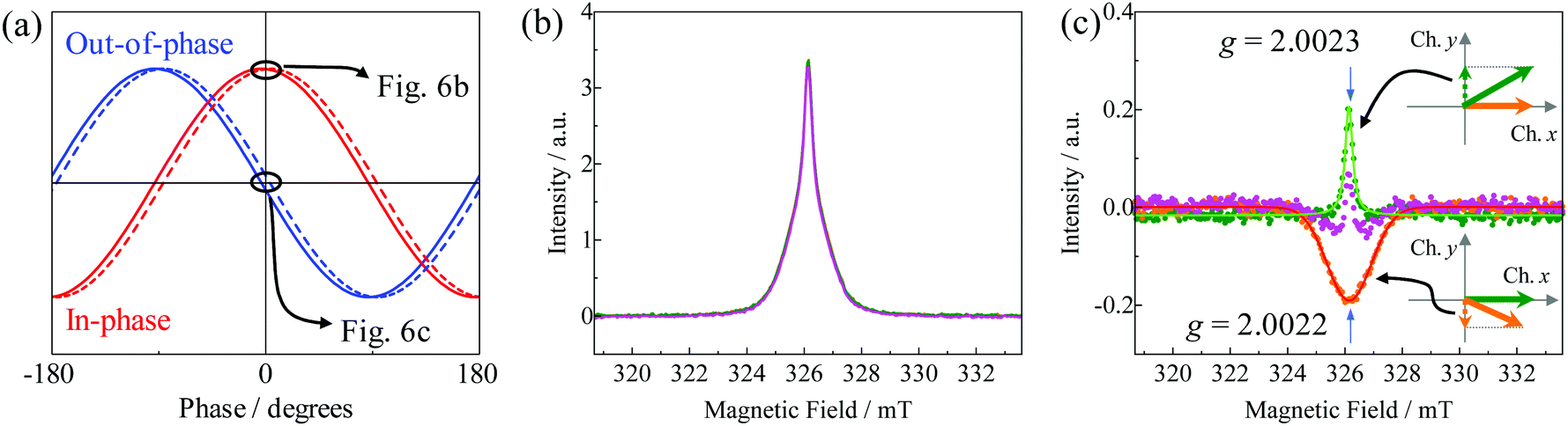
The phase dependency of the EDMR signal for the reference signal was carefully examined using the dual-phase lock-in amplifier. In this measurement, not only the amplitude of the EDMR signal was measured but also the phase difference with respect to the reference signal. When two components with different relaxation times exist in the sample, a slight phase shift between these two components is observed with respect to the reference signal. This small phase shift can be used to separate the EDMR signal components. Fig. 6a shows a schematic of the in-phase and out-of-phase detections of the two components considering that they represent different phases. For the in-phase detection, the relative intensity ratio of the two components is small, and both components are detected simultaneously. In contrast, when one of the components is adjusted to the out-of-phase, the other one is slightly shifted from the out-of-phase, leading to a large signal intensity difference of the two components in the out-of-phase detection. Fig. 6b and c correspond to in-phase (channel x) and out-of-phase (channel y) spectra at 200 K, respectively. There was relatively little difference in the in-phase spectra even when the slight phase shift was induced. In the out-of-phase detection, the slight phase adjustment led to a large difference in the relative intensities. We decomposed successfully the data into two components, in which each component was observed separately using the phase adjustment at the out-of-phase of one component. Component 1 was a Lorentzian line-shape curve with a narrow linewidth (ΔB1/2 = 0.3 mT) at g = 2.0023. Component 2 was a Gaussian line shape with a broad linewidth (ΔB1/2 = 1.8 mT) at g = 2.0022. These g-values are slightly smaller than the value of the TIPS-Pn cation radical in THF solution (g = 2.0025).44 It has been reported that the g-value becomes small when the π-orbital of pentacene is perpendicular to the magnetic field.13 The π-orbital of TIPS-pentacene is likely to be almost parallel to the substrate.46,47 In this study, the external magnetic field was applied perpendicular to the substrate. Therefore, obtaining a g-value smaller than that in solution is reasonable under the experimental conditions of this study. The two-component decomposition in the EDMR signal utilising the out-of-phase detection was reported for a ZnPc single-layer device.29 Herein, two derivative signals overlapped because a field modulation technique was used. Overlapped (not separated) EDMR signals of two-components were also reported for the pentacene-Schottky diode.15 Therein, the existence of a spin-dependent positive bipolaron formation process had been discussed, which involved the existence of a mobile polaron and trapped polaron. In our present study, the amplitude modulation technique was used to achieve the entire separation of the two signals. To explain the origin of the two components in the EDMR spectra, two possible mechanisms can be considered. One is that their components are attributed to a mobile polaron and trapped polaron, respectively, as reported in the pentacene-Schottky diode.15 Another possibility is that there are two types of e–h pairs. The TIPS-pentacene in the present system has high hole mobility and low electron mobility.48 Therefore, in the former mechanism the carriers with Lorentzian and Gaussian line-shapes can be expected to be holes and electrons, respectively. In the dynamics shown in Scheme 1, equal amounts of electrons and holes are expected to generate by photoexcitation followed by charge separation, which are as observed in the EDMR of OLEDs.22 However, in the present system, the intensity of the two components in the EDMR signal differed significantly and the area-integrated intensity of the Lorentzian component expected with higher mobility was much smaller than that of the Gaussian component with relatively low mobility. Therefore, the possibility of the former mechanism can be ruled out. In the latter possibility, the following mechanism can be considered to be the origin of the two types of e–h pairs. Since the conductivity of TIPS-Pn crystals is anisotropic, these are expected to exist in two types of e–h pairs; one consisting of carriers moving in conductive paths through the stacked pentacene plane and another belongs to a low mobility path through the migration among different planes. The EDMR spectra of e–h pairs consisting of highly mobile carriers and of relatively slow ones are expected to be the Lorentzian line-shape by the motional narrowing and the Gaussian line-shape by inhomogeneous broadening due to different local environments.
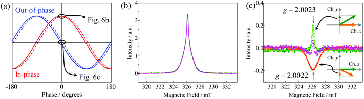 |
| | Fig. 6 (a) Model of an output function of the reference signal phase for an EDMR signal. The red and blue curves show in-phase (channel x) and out-of-phase (channel y) signals, respectively. (b) Reference signal phase dependence of in-phase EDMR spectra under the N2 atmosphere at 200 K. (c) Reference signal phase dependence of the out-of-phase EDMR spectra. | |
Conclusions
The VVD film of TIPS-Pn was evaluated by examining the temperature dependence of the photocurrent and EDMR. Their behaviours were well interpreted through the intermediate e–h pair, which existed from the singlet excited state of TIPS-Pn to the photogenerated carrier. The activation energy from the e–h pair to charge carrier was determined to be E/kB = 1103 K by temperature dependence of the photocurrent. The EDMR spectra showed the maximum intensity at approximately 200 K, which corresponded to a decrease of approximately 1.3% of the photocurrent. This was induced by ESR between the spin sublevels of the triplet state of the e–h pair. The temperature dependence of EDMR was simulated by the quantum mechanical simulation of the excited-state and carrier dynamics of the e–h pair as well as the analytical solution for the kinetic rate equation. EDMR spectra can be decomposed into two components (in which one is due to a high-mobility e–h pair and another is a low-mobility e–h pair which may be attributed to the different pathways of the conduction) using the out-of-phase signals in the quadrature detection. The linewidths of the low-mobility e–h pairs were almost independent of the temperature, while the linewidths of the high-mobility e–h pairs showed broadening due to spin–lattice relaxation at temperatures over 200 K. Therefore, the mechanism of the photoinduced carrier generation and the spin dynamics in the VVD film of TIPS-Pn (a representative photostable pentacene derivative) were elucidated in detail, which will provide useful information for the design of efficient devices utilising pentacene derivatives or similar organic semiconductor materials.
Conflicts of interest
There are no conflicts to declare.
Acknowledgements
The authors acknowledge Mr Toshio Matsuyama (technical staff for system measurements) for making the electro-circuits and Ms Masumi Hinoshita for early stage contribution for the set-up of the EDMR apparatus. The authors also acknowledge Prof. Eiji Shikoh for the AFM measurement. The present study was supported by JSPS KAKENHI (Grant Numbers JP18K19062 and JP20H02715) and JSPS KAKENHI Grant Number JP20J15238 for JSPS Research Fellow.
Notes and references
- S. Biring, Y.-Z. Li, C.-C. Lee, A. Pan, Y.-D. Li, G. Kumar and S.-W. Liu, Thin Solid Films, 2017, 636, 485–489 CrossRef CAS.
- O. D. Jurchescu, J. Baas and T. T. M. Palstra, Appl. Phys. Lett., 2004, 84, 3061–3063 CrossRef CAS.
- Y. Tani, Y. Teki and E. Shikoh, Appl. Phys. Lett., 2015, 107, 242406 CrossRef.
- Y. Tani, T. Kondo, Y. Teki and E. Shikoh, Appl. Phys. Lett., 2017, 110, 032403 CrossRef.
- Y. Tanaka, T. Kono, Y. Teki and E. Shikoh, IEEE Trans. Magn., 2019, 55, 1–4 Search PubMed.
- I. Kaur, W. Jia, R. P. Kopreski, S. Selvarasah, M. R. Dokmeci, C. Pramanik, N. E. McGruer and G. P. Miller, J. Am. Chem. Soc., 2008, 130, 16274–16286 CrossRef CAS.
- S. Katsuta, D. Miyagi, H. Yamada, T. Okujima, S. Mori, K. Nakayama and H. Uno, Org. Lett., 2011, 13, 1454–1457 CrossRef CAS.
- J. E. Anthony, J. S. Brooks, D. L. Eaton and S. R. Parkin, J. Am. Chem. Soc., 2001, 123, 9482–9483 CrossRef CAS.
- A. Maliakal, K. Raghavachari, H. Katz, E. Chandross and T. Siegrist, Chem. Mater., 2004, 16, 4980–4986 CrossRef CAS.
- Y. Kawanaka, A. Shimizu, T. Shinada, R. Tanaka and Y. Teki, Angew. Chem., Int. Ed., 2013, 52, 6643–6647 CrossRef CAS.
- A. Shimizu, A. Ito and Y. Teki, Chem. Commun., 2016, 52, 2889–2892 RSC.
- A. Ito, A. Shimizu, N. Kishida, Y. Kawanaka, D. Kosumi, H. Hashimoto and Y. Teki, Angew. Chem., Int. Ed., 2014, 53, 6715–6719 CrossRef CAS.
- K. Marumoto, S. Kuroda, T. Takenobu and Y. Iwasa, Phys. Rev. Lett., 2006, 97, 256603 CrossRef.
- H. Matsui, A. S. Mishchenko and T. Hasegawa, Phys. Rev. Lett., 2010, 104, 056602 CrossRef.
- K. Fukuda and N. Asakawa, J. Phys. D: Appl. Phys., 2017, 50, 055102 CrossRef.
- S. Singh and Y. N. Mohapatra, J. Appl. Phys., 2016, 120, 045501 CrossRef.
- R. Jia, X. Wu, W. Deng, X. Zhang, L. Huang, K. Niu, L. Chi and J. Jie, Adv. Funct. Mater., 2019, 29, 1905657 CrossRef CAS.
- W. Shockley and H. J. Queisser, J. Appl. Phys., 1961, 32, 510–519 CrossRef CAS.
-
E. L. Frankevich, Triplet State ODMR Spectroscopy: Techniques and Applications to Biophysical Systems, Wiley, 1982, ch. 5 Search PubMed.
- D. R. McCamey, H. A. Seipel, S. Y. Paik, M. J. Walter, N. J. Borys, J. M. Lupton and C. Boehme, Nat. Mater., 2008, 7, 723–728 CrossRef CAS.
- S. Hatanaka, K. Kimura, T. Suzuki and K. Kanemoto, Phys. Rev. Mater., 2018, 2, 115201 CrossRef CAS.
- K. Iwamoto, Y. Hayakawa, S. Hatanaka, T. Suzuki and K. Kanemoto, J. Phys. Chem. C, 2019, 123, 26116–26123 CrossRef CAS.
- F. Kraffert, R. Steyrleuthner, C. Meier, R. Bittl and J. Behrends, Appl. Phys. Lett., 2015, 107, 043302 CrossRef.
- S. A. J. Thomson, S. C. Hogg, I. D. W. Samuel and D. J. Keeble, J. Mater. Chem. A, 2017, 5, 21926–21935 RSC.
- R. Shoji, T. Omori, Y. Wakikawa, T. Miura and T. Ikoma, ACS Omega, 2018, 3, 9369–9377 CrossRef CAS.
- C. F. O. Graeff, M. S. Brandt, R. M. Faria and G. Leising, Phys. Status Solidi A, 1997, 162, 713–721 CrossRef CAS.
- C. F. O. Graeff, C. A. Brunello and R. M. Faria, Synth. Met., 1999, 101, 805–806 CrossRef CAS.
- W. J. Baker, T. L. Keevers, J. M. Lupton, D. R. McCamey and C. Boehme, Phys. Rev. Lett., 2012, 108, 267601 CrossRef CAS.
- S. Schaefer, S. Saremi, J. Behrends, K. Fostiropoulos, K. Lips and W. Harneit, Phys. Status Solidi B, 2009, 246, 2844–2848 CrossRef CAS.
- K. Kato, S. Hagi, M. Hinoshita, E. Shikoh and Y. Teki, Phys. Chem. Chem. Phys., 2017, 19, 18845–18853 RSC.
- S. Hagi, K. Kato, M. Hinoshita, H. Yoshino, E. Shikoh and Y. Teki, J. Chem. Phys., 2019, 151, 244704 CrossRef.
- B. J. Walker, A. J. Musser, D. Beljonne and R. H. Friend, Nat. Chem., 2013, 5, 1019–1024 CrossRef CAS.
- C. Grieco, G. S. Doucette, R. D. Pensack, M. M. Payne, A. Rimshaw, G. D. Scholes, J. E. Anthony and J. B. Asbury, J. Am. Chem. Soc., 2016, 138, 16069–16080 CrossRef CAS.
- L. Tsetseris and S. T. Pantelides, Phys. Rev. B: Condens. Matter, 2007, 75, 153202 CrossRef.
- S. Berweger, H. Zhang, P. K. Sahoo, B. M. Kupp, J. L. Blackburn, E. M. Miller, T. M. Wallis, D. V. Voronine, P. Kabos and S. U. Nanayakkara, ACS Nano, 2020, 14, 14080–14090 CrossRef CAS.
- D. Rehm and A. Weller, Isr. J. Chem., 1970, 8, 259–271 CrossRef CAS.
- G. Murtaza, I. Ahmad and J. Wu, Mater. Sci. Semicond. Process., 2015, 34, 269–275 CrossRef CAS.
- B. D. Folie, J. B. Haber, S. Refaely-Abramson, J. B. Neaton and N. S. Ginsberg, J. Am. Chem. Soc., 2018, 140, 2326–2335 CrossRef CAS.
- S. Matsuda, S. Oyama and Y. Kobori, Chem. Sci., 2020, 11, 2934–2942 RSC.
- Z. Zhou, L. Ma, D. Guo, X. Zhao, C. Wang, D. Lin, F. Zhang, J. Zhang and Z. Nie, J. Phys. Chem. C, 2020, 124, 14503–14509 CrossRef CAS.
- K. Seki and K. Marumoto, Phys. Rev. E: Stat. Phys., Plasmas, Fluids, 2019, 99, 052115 CrossRef CAS.
- W. Siebrand, J. Chem. Phys., 1967, 47, 2411–2422 CrossRef CAS.
- W. Siebrand, J. Chem. Phys., 1967, 46, 440–447 CrossRef CAS.
- S. Schundelmeier, B. Speiser, H. F. Bettinger and R. Einholz, ChemPhysChem, 2017, 18, 2266–2278 CrossRef CAS.
- A. Matsuyama, K. Maeda and H. Murai, J. Phys. Chem. A, 1999, 103, 4137–4140 CrossRef CAS.
- G. Giri, E. Verploegen, S. C. Mannsfeld, S. Atahan-Evrenk, D. H. Kim, S. Y. Lee, H. A. Becerril, A. Aspuru-Guzik, M. F. Toney and Z. Bao, Nature, 2011, 480, 504–508 CrossRef CAS.
- S. C. Mannsfeld, M. L. Tang and Z. Bao, Adv. Mater., 2011, 23, 127–131 CrossRef CAS.
- Y. Nicolas, F. Castet, M. Devynck, P. Tardy, L. Hirsch, C. Labrugère, H. Allouchi and T. Toupance, Org. Electron., 2012, 13, 1392–1400 CrossRef CAS.
Footnote |
| † Electronic supplementary information (ESI) available. See DOI: 10.1039/d0cp05125j |
|
| This journal is © the Owner Societies 2021 |
Click here to see how this site uses Cookies. View our privacy policy here. 
 Open Access Article
 This Open Access Article is licensed under a Creative Commons Attribution-Non Commercial 3.0 Unported Licence
 *
*