
Dielectric confinement for designing compositions and optoelectronic properties of 2D layered hybrid perovskites
Rayan
Chakraborty
 * and
Angshuman
Nag
*
* and
Angshuman
Nag
*
Department of Chemistry, Indian Institute of Science Education and Research (IISER), Pune, 411008, India. E-mail: rayan.chakraborty@students.iiserpune.ac.in; angshuman@iiserpune.ac.in
First published on 24th November 2020
Abstract
Two dimensional (2D) layered hybrid lead halide perovskites are a fascinating class of semiconductors displaying a plethora of interesting optoelectronic properties with potential for application in solar cells, light emitting diodes, etc. Most of these properties can be linked to their repeating quantum well-like structures providing 2D excitons. In this perspective, we discuss how dielectric confinement of excitons originates in these layered hybrid perovskites, and then, how it can be used to tune the excitonic properties. In particular, we discuss the recent theoretical and experimental advances correlating dielectric confinement with chemical composition, excitonic binding energy, and optoelectronic property. The freedom from the restrictions of the Goldsmith tolerance factor allows the synthesis of hundreds of compositions of 2D layered hybrid perovskites by independently varying the organic and inorganic layers. We envisage that the combination of this compositional flexibility with the concepts of dielectric confinement discussed in this perspective would be a path forward for designing novel optoelectronic materials.
 Rayan Chakraborty | Rayan Chakraborty did his Bachelor of Science with Chemistry Major from the University of Calcutta in 2015. Since 2015, he has been an integrated PhD student in the Department of Chemistry at IISER Pune. His research interests are excitons in low-dimensional perovskites and catalysis on semiconductor surfaces. |
 Angshuman Nag | Angshuman Nag received his Master of Science in Chemistry from Indian Institute of Technology Guwahati in 2003. Then he received his PhD degree from Indian Institute of Science Bangalore in 2009. He then completed two terms as a postdoctoral researcher at Indian Institute of Science Bangalore and at the University of Chicago. He joined IISER Pune in 2012 as a Ramanujan Fellow. Presently, he as an Associate Professor of Chemistry at IISER Pune. His current research is on developing perovskite semiconductors for optoelectronic applications. |
A. Introduction
After staying nearly forgotten for over a few decades, in the last five years, two-dimensional (2D) layered hybrid lead halide perovskite semiconductors have reattracted intense research interest. This sudden excitement is majorly owing to the success of their three-dimensional (3D) counterparts in high-efficiency optoelectronic applications, including solar cells.1–12 The subclass of 2D layered perovskites has already proven to be important optoelectronic materials with high photovoltaic and light-emitting efficiencies, along with improved moisture stability compared to their 3D analogues.13–17 However, the underlying chemistry and physics behind the fascinating optoelectronic properties of these layered perovskites are not yet completely understood.The critical difference in the 2D layered hybrid perovskite from 3D analogues arises from the loss of connectivity of the Pb-halide network in one direction. In the 3D APbX3 lattice (Fig. 1a), the small A-site cations like Cs+ and CH3NH3+ (methylammonium; MA) occupy the cuboctahedral void formed by eight lead-halide octahedra. Substitution of these smaller A-site cations with larger ones like butylammonium (BA) or phenyl ethyl ammonium (PEA) breaks the Pb–X–Pb chain in one direction (see Fig. 1b), forming compositions such as A2PbX4. Since the limits of the Goldsmith tolerance factor18 are not applied for such layered structures, a wide variety of compositions and structures of 2D layered perovskites have already been reported.19–26
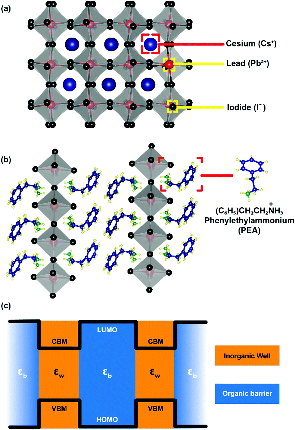 | ||
| Fig. 1 Structural differences between 3D and 2D layered perovskites. (a) 3D CsPbI3 lattice, the grey octahedra with black vertices are [PbI6]4− units, and blue balls are Cs+ ions. (b) 2D (PEA)2PbI4 lattice, PEA = phenylethylammonium. (c) Band edge energy alignment in the 2D halide perovskite. CBM and VBM are the conduction band minimum and the valence band maximum respectively for an inorganic well with high-frequency dielectric constant εw. HOMO is the highest occupied molecular orbital and LUMO the lowest unoccupied molecular orbital of an organic barrier with high-frequency dielectric constant εb. | ||
The organic layers have a higher energy gap compared to the inorganic layer forming a type-I band alignment at the organic/inorganic interface (see Fig. 1c).27 Therefore, in 2D layered hybrid perovskites, both electrons and holes are strongly quantum confined in the atomically thin (∼6.4 Å) inorganic semiconducting well separated by insulating organic barriers. The organic (barrier)/inorganic (well) structures get repeated, forming a naturally repeating quantum well structure (Fig. 1c).
In addition to this repeating quantum well structure, the dielectric medium also changes repeatedly between the organic and inorganic medium. How this dielectric contrast influences the optical properties and optoelectronic applications of layered perovskites? In this perspective article, we provide insights to answer this question. The approach here is to connect the long known concepts of semiconductor physics with recent experimental and theoretical developments in layered hybrid perovskites. The remaining part of the manuscript is divided into the sub-divisions, namely, excitons, quantum and dielectric confinement, recent theoretical advancement, recent experimental advancement, and finally, conclusion and future outlook. It is to be noted here that for the entire article, the dielectric constant refers to the high frequency (optical) dielectric constant solely arising from electronic polarization.
B. Exciton
Excitons govern the optical and optoelectronic processes in a semiconductor. When a semiconductor absorbs a quantum of a photon of desired energy, then an electron gets excited from its valence band to the conduction band (Fig. 2). The photo-exited electron in the conduction band and the hole in the valence band attract each other with Coulomb force (F). The attractive force provides additional stability by holding the photogenerated electron and hole together. This electron–hole pair is termed as an exciton. The modulus of this attractive force depends on the physical distance (r) between the electron and the hole and the dielectric constant (ε) of the lattice, along with constant elementary charge (e), as shown in the Coulomb equation. | (1) |
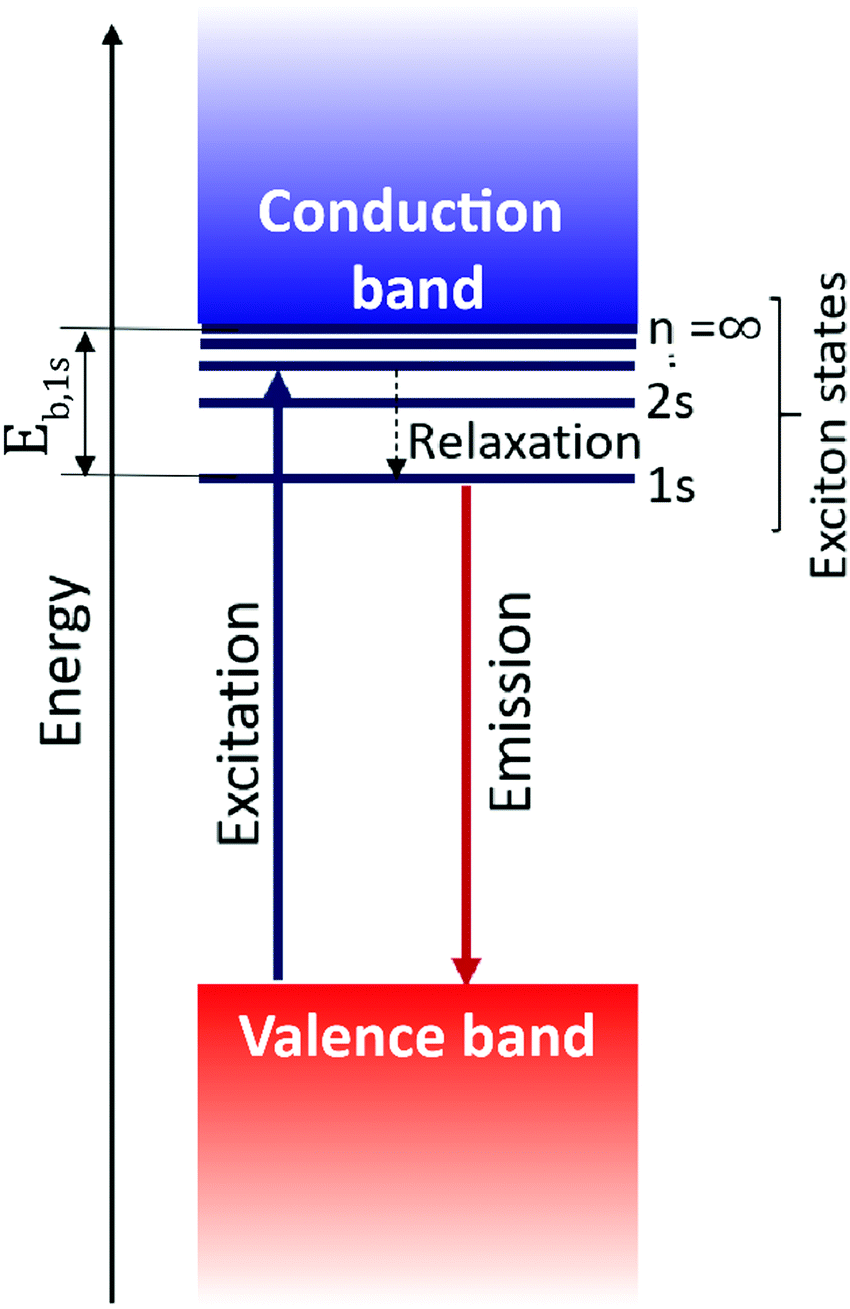 | ||
| Fig. 2 Schematic of the formation of an exciton and definition of excitonic binding energy. N (= 1, 2, 3…) represents the excitonic energy levels, and Eb,1s is the binding energy of the 1s exciton. Typically, excitonic binding energy refers to the 1s excitonic binding energy, Eb,1s. | ||
Being a quantum mechanical particle, an exciton is affected by spatial confinement the same way as the “particle in a box” model predicts. As a consequence of this, the electron–hole wavefunction overlap increases, or the excitonic binding energy increases. In 2D layered perovskites, strong spatial quantum confinement is operational because of their quantum well like architecture. Interestingly, the stark contrast of dielectric constant between the well and barrier layer adds another excitonic confinement – this is known as the dielectric confinement effect.
C. Quantum and dielectric confinement
Like the Bohr hydrogen model gives out the 3D Mott–Wannier excitonic model, an analogous 2D Schrödinger equation for the electron and hole (also called the 2D Wannier model) can be constructed for an exciton confined in a 2D semiconductor medium.29 It turns out that the energies of the 2D excitonic states have a resemblance to the 3D-exciton model. For excitonic states with N = 1, 2, 3,…, the energy is expressed by the following equation: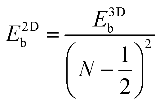 | (2) |
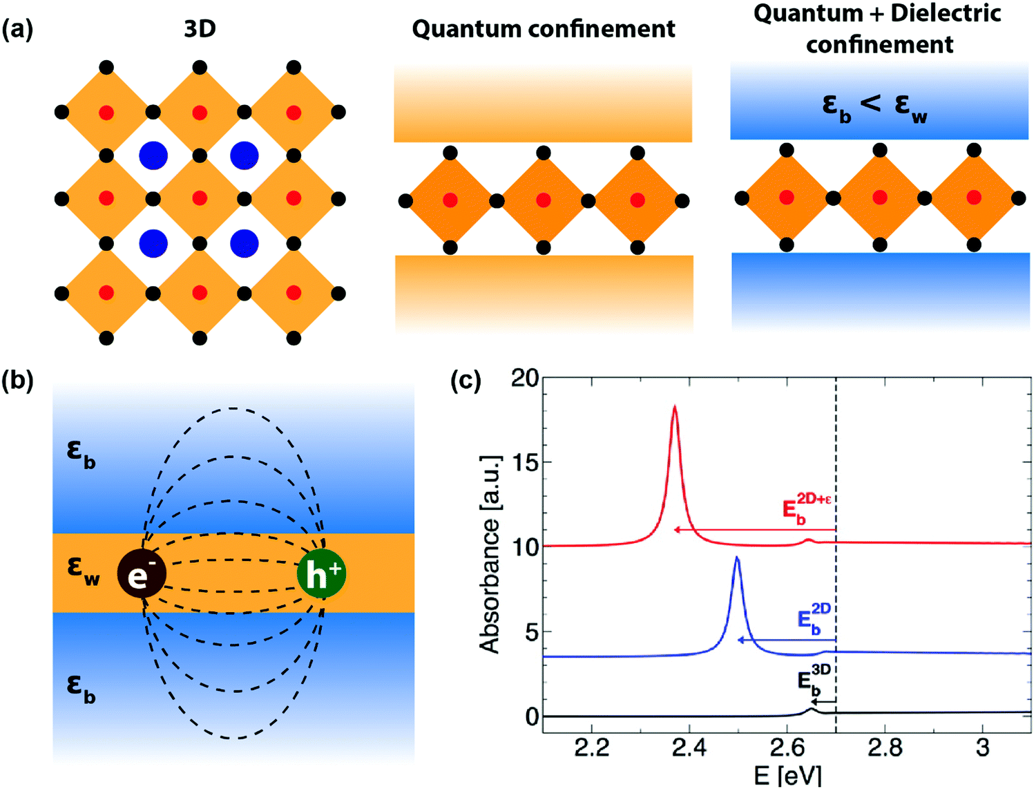 | ||
| Fig. 3 Quantum and dielectric confinement effects. (a) Illustration of quantum confinement (assuming a constant high-frequency dielectric constant for both well and barrier) and dielectric confinement in 2D layered perovskites, compared to a 3D perovskite system. Here, εw and εb are the high-frequency dielectric constant of the well and barrier layers, respectively. (b) Schematic of the dielectric confinement in a quantum-well structure. The dashed lines indicate the attractive force acting between the electron and the hole. Note that the attractive lines of forces are spread over both inorganic and organic layers, even though the electron and the hole are residing in the inorganic well. (c) Simulated effect of quantum and dielectric confinement on optical absorption due to 1s excitons. The band gap is set at 2.7 eV, indicated by the vertical dashed line. The black line is the absorbance spectra computed on a hypothetical 3D system having the same high-frequency dielectric constant as that of the well layer (εw). The small excitonic binding energy, E3Db, corresponds to the 3D exciton. Turning on the quantum confinement effect while keeping the dielectric constant homogeneous shifts the resonance peak at lower energy (blue line), and further incorporating the dielectric confinement results in an additional shift and an enhanced excitonic resonance (red line). Reprinted with permission from ref. 35, Copyright (2016) American Chemical Society. | ||
To address this issue, dielectric confinement was prescribed, on top of the spatial quantum confinement. Dielectric confinement arises due to the contrast of the dielectric constants between two subsequent layers in a quantum-well structure (right panel of Fig. 3a). It was theoretically studied by Rytova, Keldysh, and later by Muljarov for thin semiconductor films sandwiched between two layers of different dielectric constants.36,37 The idea stems from the fact that the electrical force field of Coulomb attraction between electron and hole in an exciton residing in the well layer would also penetrate the barrier layer (Fig. 3b). Therefore, the high-frequency dielectric constant of both the barrier (εb) and well (εw) will determine the Coulomb force. If εb is significantly less than εw, then the net decrease in charge screening increases the Coulomb force, increasing the excitonic binding energy. Such an increase in excitonic binding energy or excitonic confinement because of dielectric contrast in the medium (εb < εw) is termed here as dielectric confinement.38
Keldysh's formula for 1s excitons relates the excitonic binding energy in a 2D well of width zero and infinite barrier potential with different εw and εb, with the corresponding 3D system with a homogeneous dielectric constant equal to εw:
 | (3) |
 with the numerator of eqn (2) brings us to eqn (3) for the case of N = 1. Here, E2D+εb denotes the excitonic binding energy of the 1s exciton, taking both quantum and dielectric confinements into consideration.
Experimentally, the effect of dielectric confinement should be observable in the excitonic resonance signals in optical absorption and photoluminescence spectra. While separation of quantum and dielectric confinement effects is difficult by experimental means, computational simulation allows one to visualize the impact of both kinds of confinement on an excitonic absorption peak (Fig. 3c). First, the quantum confinement increases the excitonic binding energy E2Db, shifting the excitonic absorption peak to the lower energy side. Then the addition of dielectric confinement further increases the excitonic binding energy E2D+εb, further red-shifting the excitonic resonance peak.35 In both cases, the excitonic absorbance intensity increases since the incorporation of the confinements results in higher oscillator strength of the excitons.
Quantum-well heterostructures are a potentially suitable testbed for studying the effect of dielectric confinements. The III–V semiconductors like GaAs/InAs/GaAs are expected to show such dielectric confinement of excitons following eqn (3).39,40 But in these heterostructures, both the well and the barrier are of very similar chemical nature, yielding  ratio ∼1. Similar is the case for heterostructures of II–VI semiconductors.41,42 So any significant effect of dielectric confinement is often not observed. In contrast, in layered 2D hybrid perovskites, the dielectric mismatch between the inorganic well and the organic barrier layer is large and the alignment of the energy levels of the well and the barrier is that of type-I. Moreover, since both the well and the barrier are part of the same crystal structure, the problem of lattice mismatch does not appear in these systems. For example, in the much-studied (BA)2PbI4, the
  ratio is expected to be close to 3.43 As a result, the enhancement of E2D+εb in 2D layered hybrid perovskites is much more significant than what has been observed in the III–V quantum-well heterostructures.
D. Recent theoretical advances
Although the experimental observations of binding energy enhancement in 2D perovskites can qualitatively be explained by eqn (3), it is far more challenging to come up with a theoretical model that can quantitatively predict the E2D+εb values for different compositions. The hindrance lies on multiple fronts – (i) the organic cation layer (BA+) and the inorganic anion layer (PbI42−) in (BA)2PbI4 do not exist separately. So, εw and εb cannot be measured. (ii) E3Db cannot be obtained since the 3D counterpart of the inorganic well does not exist. In the absence of values for εw, εb, and E3Db, eqn (3) becomes ineffective to calculate E2D+εb. In general, modeling of the organic/inorganic interface is computationally resource-intensive due to the abrupt changes in the dielectric profile.37,44,45One of the interesting recent advances to address the issue has been the so-called “composite approach.”44,46 In this approach, the layered structure is treated as a composite of a charge-neutral perovskite well and an organic barrier sub-lattice. For example, Fig. 4a shows how a Ruddlesden–Popper perovskite (BA)2(MA)4Pb5I16 is treated in this model. The perovskite (W) layer is assumed as Cs2(MA)4Pb5I16 by replacing BA with Cs. The organic (B) layer is considered as (CH3(CH2)3CH3)2 by replacing NH3+ of BA with CH3. The final composite W/B is considered as a model system for (BA)2(MA)4Pb5I16. Using this composite model, Traore et al. computed the position-dependent high-frequency dielectric constant profile for both W and B layers, as shown in Fig. 4b.46 The obtained values for dielectric constants are found to be 1.9 for the B-layer and 5.5 for the W-layer. The difference arises from the different nature of the chemical bonds that form in the organic and inorganic layers. These values highlight the presence of dielectric confinement in 2D layered perovskites following eqn (3). Interestingly, the addition of dielectric profiles for W and B overlaps with the dielectric profile computed for the W/B composites. These results suggest that the dielectric profile of (BA)2(MA)4Pb5I16 can be computed using the W/B composite model, ignoring the interaction at the interface of W and B. Similarly, the composite model could also explain the electronic band alignment at the interface of W/B composites. Thus, this model enables affordable computation of the confinement effects on the electronic states in samples like (BA)2(MA)4Pb5I16 with a larger width of the well and a fewer number of W/B interfaces. However, in systems like (BA)2PbI4 with a mono-layer thick well, the interface dominates the electronic properties, and the composite approach fails to explain the experimental results.
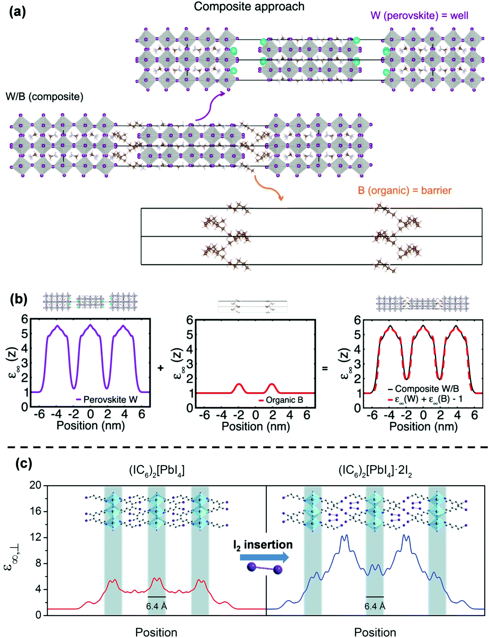 | ||
| Fig. 4 Theoretical modeling of confinements in 2D hybrid halide perovskites. (a) Schematic of the composite approach for computing the high-frequency dielectric profile. The top and the bottom panel show the perovskite well (W) Cs2(MA)4Pb5I16 and the organic barrier (B) (CH3(CH2)3CH3)2, respectively. The middle panel is the W/B composite structure representing a model system for layered perovskites (BA)2(MA)4Pb5I16. (b) The position-dependent high-frequency dielectric constant (ε∞(Z)) profile of the lattice computed using the composite approach. (c) DFT computed position-dependent high-frequency dielectric profile of pristine (1-iodohexylammonium)2PbI4 and the effect of incorporation of I2. A highly polarizable I2 molecule increases the dielectric profile's amplitude in the barrier region. Panels (a and b) are reprinted with permission from ref. 46, Copyright (2018) American Chemical Society. Panel (c) is reprinted after slight modifications from ref. 47 published by The Royal Society of Chemistry. | ||
These results suggest that to estimate the impact of confinements in layered perovskites with a monolayered-thick well, one needs to use the more precise atomistic description of the interface.48–50 This approach was taken up by Smith et al. to calculate the effect of confinement on electronic states and further on excitonic binding energies.47 They calculated the dielectric profile of (1-iodo-6-hexylammonium)2PbI4 using density functional theory (DFT), as shown in Fig. 4b. Similar to the composite approach, the difference in the high-frequency dielectric constants between the well and barrier layer could be visualized, suggesting the origin of dielectric confinement. They observed that intercalating I2 in the barrier layer increases the dielectric constant of the barrier. Furthermore, the change in the dielectric constant of the barrier layer has an impact on the dielectric constant of the inorganic well layer as well. In other words, dielectric constants of the well and barrier are not entirely independent of each other, unlike the previously discussed composite approach. Experimentally, by measuring the optical absorption spectra of the samples at 5 K, they observed that the excitonic binding energy (E2D+εex) decreases in the I2 intercalated structure. To obtain a theoretical model for this observation, the authors attempted to calculate the excitonic absorption spectra using a semi-empirical method without any input from the experiments. They observed that the theoretically calculated E2D+εex values only qualitatively agree with the experimentally observed trend.
A better quantitative agreement between theoretically and experimentally obtained values of E2D+εex requires a better estimation of the reduced effective mass of the exciton, μ. It has been shown that standard approximations that are used to extract μ from ab initio calculations fail in these systems because of the nonparabolicity of the band dispersions in the stacking direction.44,46,51 So, at present, one needs to bank on experimental measurements to obtain the reduced mass, which can, after that, be fed into the computational workflow to obtain E2D+εb. This approach was recently shown to be able to predict E2D+εb values quite accurately, albeit with a slightly different version of theory than the ones presented in this section.52
The major problem for the computational studies is the huge computational cost imparted by multiple factors. Firstly, all 2D perovskites have much larger unit cells with lower symmetry along with higher number of atoms compared to their 3D analogues. Second, due to the presence of multiple organic cations, obtaining the accurate ground-state relaxed geometry requires the dispersion forces to be incorporated.47,53 Third, the description of Pb valence electrons requires the relativistic spin–orbit coupling (SOC) to be taken into account.54–56 Also, the standard flavour of DFT (only solving for the Kohn–Sham (KS) states) inherently tends to underestimate the bandgaps of semiconductors. So, either hybrid DFT functional based approaches or employing more resource intensive many-body approaches like GW is the way forward for obtaining better approximations of the electronic states.57–59 Furthermore, to obtain the excitonic levels one needs to solve the Bethe–Salpeter equation (BSE) to take into account the electron–hole interaction or utilize time-dependent DFT (TDDFT).60–63 In the end, all these factors make the entire theoretical exercise for obtaining the excitonic binding energy a resource-demanding venture.
E. Recent experimental advances
Experimentally, the effect of dielectric confinement was observed in the late 1990s. In this review, we will not discuss those early approaches in detail. Interested readers are recommended to read a more elaborate review on the subject written by Katan et al.64 In this section, we will highlight recent developments, where dielectric confinement has been tuned by rational design of compositions of 2D layered perovskites. Consequently, E2D+εb values have been tuned by order of magnitude. Such a wide range of tunable E2D+εb enhances the potential optoelectronic applications of 2D layered perovskites. This section is further divided into three sub-sections.E.1 Excitonic binding energy of Ruddlesden–Popper (BA)2(MA)n−1PbnI3n+1 perovskites with varying thickness of the well
In recent years, various compositions of Ruddlesden–Popper65 and Dion-Jacobson66 phases of layered hybrid perovskites have been prepared. One example of Ruddlesden–Popper layered perovskites is (BA)2(MA)n−1PbnI3n+1 (see Fig. 5a). In this series of samples, the width of the inorganic well layer can be tuned between 0.64 nm for n = 1 and 3.14 nm for n = 5.52 This provides an experimental handle to study the effect of both quantum and dielectric confinement on excitonic binding energy with variation in well thickness. Blancon et al. estimated the excitonic binding of (BA)2(MA)n−1PbnI3n+1 for n = 1 to 5, using optical density (OD) (UV-visible absorption spectra) and photoluminescence excitation (PLE) measurements at 4 K. Fig. 5b shows representative spectra for the sample with n = 4. Optical transitions corresponding to 1s, 2s, and 3s excitonic states are observed. Analysis of the 2s, 3s Rydberg series leads to the estimation of the electronic band gap (Eg) between the continuum valence and conduction band. Then the binding energy for 1s excitons is obtained as E2D+εb = Eg − E1s, where E1s is the peak energy for 1s excitonic absorption shown in Fig. 5b.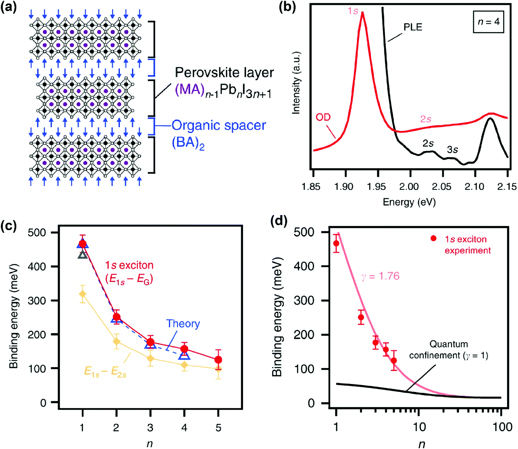 | ||
| Fig. 5 Excitonic binding energy of the (BA)2(MA)n−1PbnI3n+1 layered perovskite with n = 1 to 5. (a) Schematic structure of a sample with n = 3. (b) Optical density (OD) and photoluminescence excitation (PLE) spectra measured at 4 K on mechanically exfoliated films of a sample with n = 4. (c) Comparison of 1s excitonic binding energy obtained from experimental (OD and PLE) data with theoretically calculated values. Also, experimentally observed energy differences between 1s and 2s excitonic states are plotted. (d) Fitting of experimentally observed exciton binding energy with an empirical scaling law given in eqn (4). All panels are reprinted with permission from ref. 52 published by Nature Communications. | ||
Fig. 5c shows that the 1s excitonic binding energy decreases with the increasing width (n) of the well. The experimental data agree well with theoretical data. Note that the theoretical calculations were possible by using experimentally (magneto-optic study) obtained μ as input parameters.52 The decrease in excitonic binding energy with increasing “n” is expected because the increase in the width of the well decreases the quantum confinement. In addition, the increase in well width is also likely to reduce the relative spread of the excitonic force field in the barrier layer, influencing the dielectric confinement. Furthermore, a change in “n” also modifies the chemical composition of the well. So, a change in “n” can also introduce minor changes in εw.
To have more insights into the contribution of quantum and dielectric confinement, an empirical scaling law was developed.52 The scaling law is of the form
 | (4) |
E.2 Tuning dielectric confinement by halide composition
Both the homogeneous ε in 3D systems like CsPbX3 and εw in a 2D system like (PEA)2PbX4 change with the halide ion composition. Expectedly, such a difference in the dielectric environment strongly influences the excitonic binding energy. Both ε in 3D CsPbX3 and εw in 2D (PEA)2PbX4 increase with halide composition changing from Cl to Br to I (Fig. 6a). This increase in the dielectric environment is expected since a decrease in the electronegativity of the halide prompts an enhancement in the electronic polarizability of the metal–halide bond. For 3D systems, an increase in ε decreases the excitonic binding energy, following eqn (1). This decrease in excitonic binding energy implies a reduced overlap of electron and hole wavefunctions, resulting in reduced transition probabilities for optical absorption and emission. Subsequently, an increase in average photoluminescence lifetime (τ3Dav) is observed by varying X from Cl to Br to I in CsPbX3 and other 3D perovskites (Fig. 6b). An opposing trend in average photoluminescence lifetime (τ2D+εav) is observed for 2D (PEA)2PbX4. Fig. 6c shows that the τ2D+εav of (PEA)2PbX4 decreases when varying X from Cl to Br to I. This trend in τ2D+εav suggests that the excitonic binding energy of 2D (PEA)2PbX4 increases from Cl to Br to I.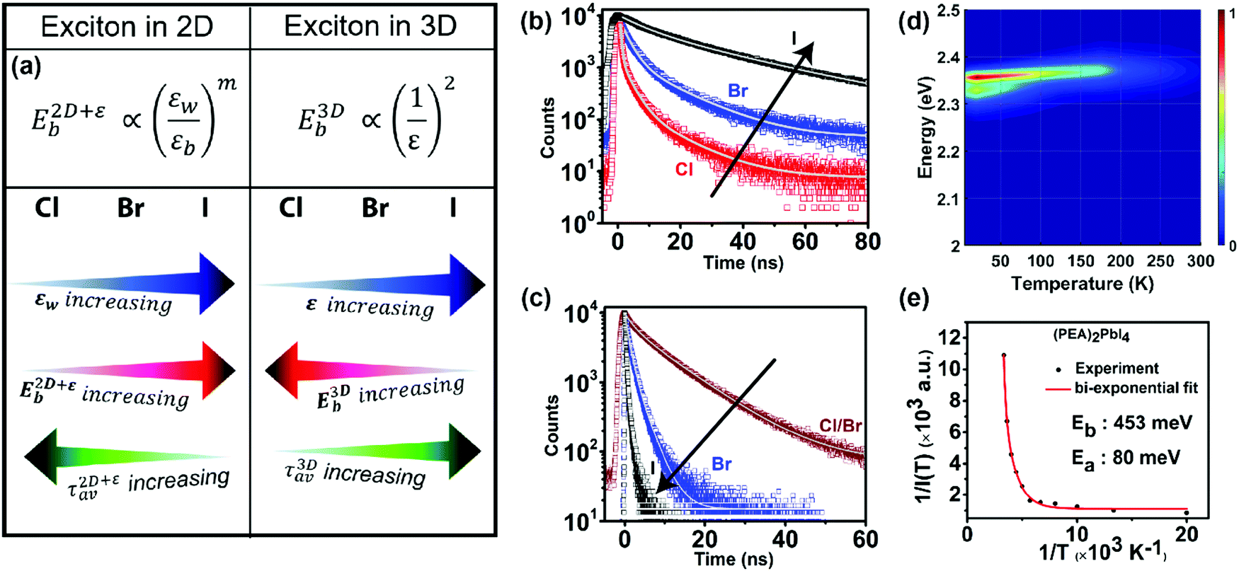 | ||
| Fig. 6 Effect of modifying the high-frequency dielectric constant of the inorganic layer (εw) by controlling halide composition. (a) Schematic showing correlation of halide compositions of 2D and 3D perovskites with their excitonic binding energies (E2D+εb and E3Db) and average photoluminescence lifetimes (τ2D+εav, and τ3Dav). εw, and εb are the high-frequency dielectric constant of the inorganic well layer and the organic barrier layer, respectively, in the 2D perovskite. ε is the high-frequency dielectric constant of the 3D perovskite. Photoluminescence decay dynamics of (b) colloidal CsPbX3 (X = Cl, Br, I) perovskite nanocrystals dispersed in hexane, and (c) (PEA)2PbX4 (X = Cl/Br, Br, I) perovskite films. The arrows in (b and c) indicate the change in average photoluminescence lifetime with halide composition. (d) The pseudocolor map of temperature-dependent emission intensity of (PEA)2PbI4 films. The vertical colored bar indicates the normalized emission intensity scale. (e) Experimentally obtained inverse of integrated PL intensity [1/I(T)] vs. inverse of temperature (1/T) plots fitted using a bi-exponential decay equation (eqn (7)), for (PEA)2PbI4. All panels are reprinted after slight modification with permission from ref. 34, Copyright (2020) American Chemical Society. | ||
Fig. 6a summarizes the opposite trends in 3D and 2D excitons. E3Db increases with decreasing ε following eqn (1). In contrast, E2D+εb increases with increasing εw. This contrast is because of the dielectric confinement effect in the 2D layered perovskite, because of which E2D+εb ∝ (εw/εb)m, where m is an unknown positive number and εw > εb. This experimental finding is qualitatively similar to eqn (3).
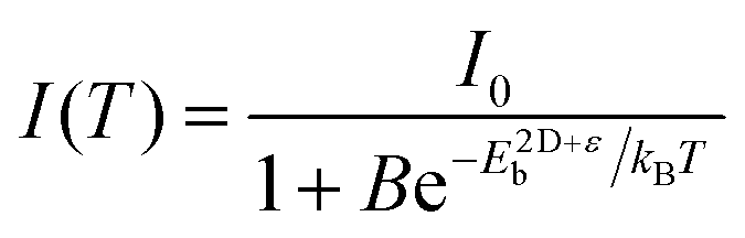
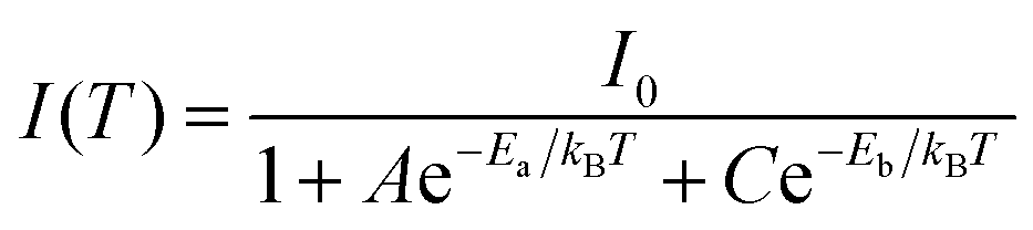
An increase in temperature provides the energy to dissociate excitons and thereby reducing photoluminescence intensity. So, one can quantitatively estimate E2D+εex by analysing the temperature-dependent change in photoluminescence intensity.67Fig. 6d shows the pseudocolor maps of temperature-dependent photoluminescence spectra of (PEA)2PbI4. Expectedly, photoluminescence intensity increases with decreasing temperature. This temperature (T) dependence of integrated photoluminescence intensity, I(T), is given by eqn (5), where kB is the Boltzmann constant:
 | (5) |
 | (6) |
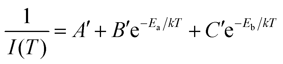
Now eqn (6) can be rearranged as bi-exponential decay in eqn (7), where A′ = 1/I0, B′ = A/I0, and C′ = C/I0.
 | (7) |
E.3 Tuning dielectric confinement by controlling the organic layer
As discussed above, E2D+εb ∝ (εw/εb)m. So, tailoring the organic layer (εb) can be an interesting approach to modify E2D+εb. An interesting case is (EA)2PbI4, where EA (=ethanolammonium) is a highly polarizable organic cation. εw is similar for both (EA)2PbI4 and (PEA)2PbI4. But εb = 37.7 for (EA)2PbI4, which is very high compared to εb = 3.3 of (PEA)2PbI4;69 therefore, one would not expect dielectric confinement in (EA)2PbI4. Indeed, E2D+εex estimated for (EA)2PbI4 using temperature-dependent photoluminescence is only about 65 meV, as compared to the high E2D+εex = 453 meV obtained for (PEA)2PbI4.34 This low E2D+εex for (EA)2PbI4 points out to the possibility of synthesising 2D layered perovskites with low excitonic binding energy. The compositions with small excitonic binding energies are desirable for applications like photovoltaics.In another interesting report, Passarelli et al. reported the tuning of εb and E2D+εb by doping the organic layers.70 They used a naphthalene cation (Nap) based organic layer for the formation of layered perovskites like (H–Nap–O–Pr–NH3+)2PbI4 (where Pr is propyl). The schematic structure and different compositions of perovskite samples numbered 1 to 8 are shown in Fig. 7a–c. Molecular doping of tetrachloro-1,2-benzoquinone (TCBQ) in the organic layer of (H–Nap–O–Pr–NH3+)2PbI4 (sample number 2) is shown in Fig. 7a. In the doped lattices, TCBQ is an electron-accepting and naphthalene is an electron-donating species forming donor–acceptor complexes, which drives the doping of TCBQ. Interestingly, the low-temperature optical absorption data show that TCBQ doping significantly changes the energy of 1s excitonic transitions, without changing the electronic bandgap of (H–Nap–O–Pr–NH3+)2PbI4. In other words, the 1s excitonic binding energy changes with the molecular doping. Undoped (H–Nap–O–Pr–NH3+)2PbI4 exhibits E2D+εb = 400 meV, whereas with 0.5 and 1 equivalent (with respect to the PbI2 precursor) TCBQ doping, E2D+εb decreases to 310 and 230 meV, respectively. This tunability of E2D+εb with molecular doping is attributed to the dielectric confinement effect. The electron donor–acceptor complexation further stabilizes the π–π interaction between TCBQ and naphthalene rings. In this process, the electron density increases in the electron acceptor TCBQ, reducing the electron density of the naphthalene ring introducing a partial positive charge (see the right panel of Fig. 7a). Therefore, TCBQ doping creates a more polarizable organic layer increasing the εb. Consequently, (εw/εb) and E2D+εb decrease with the increasing doping of TCBQ.
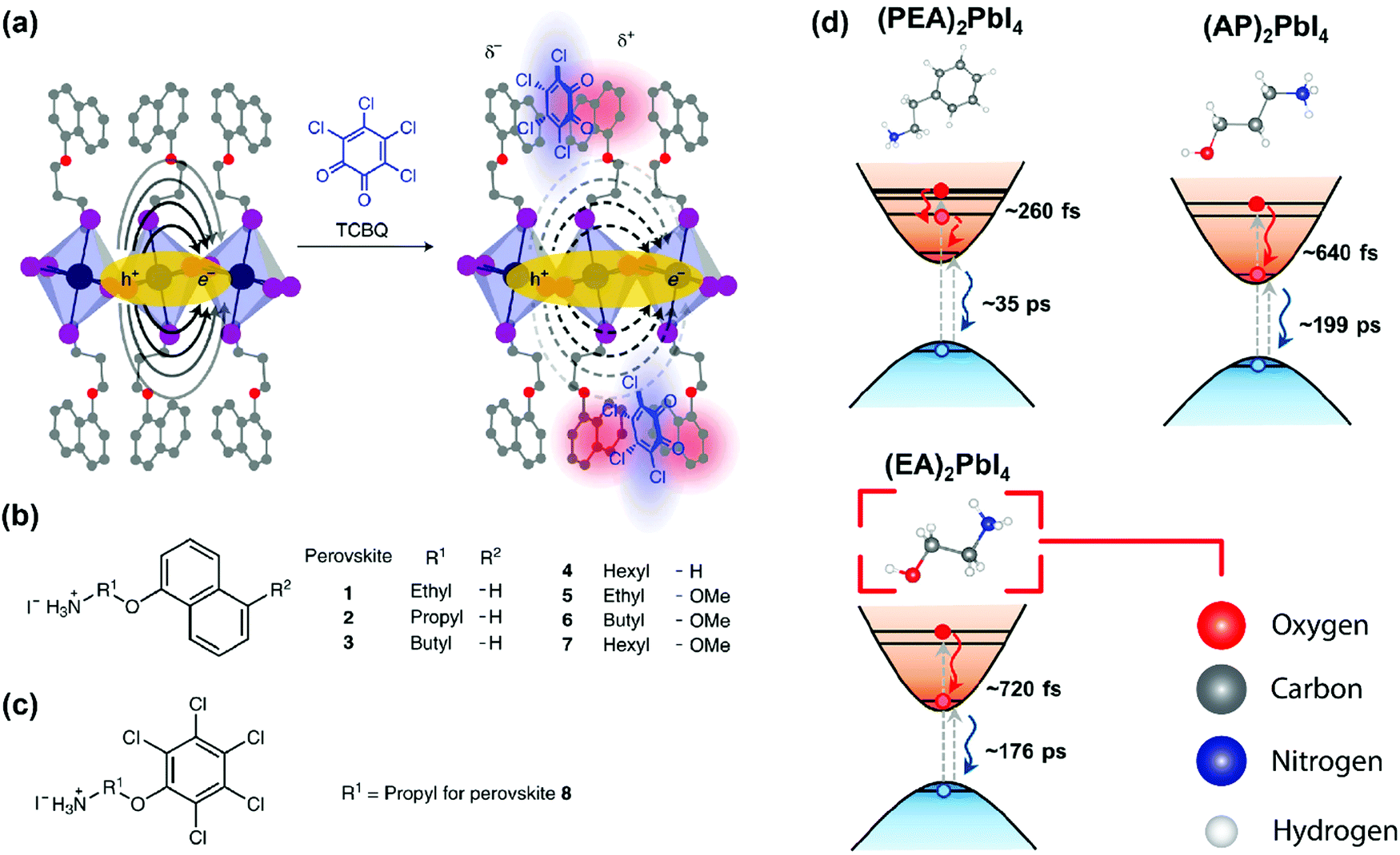 | ||
| Fig. 7 Effect of modifying the high-frequency dielectric constant (εb) of the organic layer. (a) Incorporating a molecular dopant (TCBQ) to induce a donor–acceptor type interaction in the organic layer. Consequently, the high-frequency dielectric constant increases, and the organic layer can screen the charges better. This, in turn, reduces the binding energy of the exciton. The solid oval arrows in the left-hand side figure indicate the force-field acting between the electron and the hole; the dashed arrows in the right-hand side figure indicate the modified force field due to the presence of the dopant. In this figure, carbon, oxygen, nitrogen, lead, and iodine atoms are shown in grey, red, blue, indigo, and purple, respectively. (b and c) Different compositions of organic cations that are used in the 2D layered perovskite for this study. (d) Schematic showing the hot carrier cooling process. Increasing εb increases the hot-electron relaxation time. For PEA (εb ∼ 3.3) the relaxation time is 260 fs, and it is increased to 720 fs when EA (εb ∼ 37) is used. The color code for the atoms in this figure is shown in the lower right panel. Panels (a–c) are reprinted with permission from Springer Nature-Nature Chemistry reference70 Copyright (2020). Panel (d) is reprinted after slight modifications with permission from ref. 69, Copyright (2019) American Chemical Society. | ||
Finally, we discuss an example where the dielectric constant of the organic layer can also influence the ultrafast carrier dynamics. Absorption of photons with energy much higher than the band gap creates hot carriers. Schematics in Fig. 7d show the process considering hot electrons. The hot electrons then non-radiatively relax down to the conduction band minimum within a few hundreds of femtoseconds. This relaxation process is termed as hot carrier cooling. If the cooling time for hot electrons can be increased, the possibility of extraction of such high energy carriers for photovoltaic and catalytic applications increases. Yin et al. showed that the hot career cooling dynamics has a dependency on the dielectric contrast in 2D layered perovskites.69 They used three different kinds of organic ammonium cations, PEA (εb ∼ 3.3), 3-aminopropanol (AP, εb ∼ 28), and EA (εb ∼ 37), for A2PbI4. Interestingly, the hot carrier cooling time increases systematically with increasing εb from (PEA)2PbI4 to (AP)2PbI4 to (EA)2PbI4, as shown in Fig. 7d. Detailed experimental and theoretical studies suggest that the increase in hot carrier cooling time can be attributed to multiple factors, including stronger screening of the Coulomb interactions with increasing εb.69
The tunability of the excitonic properties by altering the organic layer composition offers more possibilities compared to the inorganic layer because of the availability of a large number of organic ammonium cations. In recent years, several works have been published employing this strategy.71–74 In one of the notable works, the vapor-fumigation technique enabled the formation of 2D MA2PbI4 thin films.72 MA having a much larger dielectric constant (εb ∼ 11) compared to traditional aliphatic cations (like BA) enabled a reduced excitonic binding energy (E2D+εex ∼ 172 meV). This consequently results in more efficient free carrier formation, and thus, the highest photovoltaic efficiency (16.6%) for a 2D perovskite was obtained.
F. Conclusions and future outlook
In the 1990s, it was explored that dielectric confinement influences the excitonic binding energy of 2D layered hybrid perovskites. In the last few years, the research focus has been on two major aspects of dielectric confinement – (i) quantitative estimation of the dielectric confinement effect on excitons, and (ii) tailoring the optical and optoelectronic properties by utilizing the dielectric confinement. Here we provide our perspective on these recent developments. We observed that E2D+εb ∝ (εw/εb)m, where m is a non-zero positive number, probably closer to 2. Here, εw and εb can be easily controlled by fine-tuning the chemical composition of inorganic and organic layers, respectively, without altering the size and structure of the crystal. Consequently, dielectric confinement can tune E2D+εb by order of magnitude in the range of a few tens to a few hundreds of meV, without changing the spatial quantum confinement effect. Such extraordinary tunability of excitonic binding energy using dielectric confinement is a unique attribute of 2D layered hybrid perovskites. Subsequently, one can tune the optical absorption and emission energies, and their transition probabilities (absorption cross-section and photoluminescence lifetime), simply by controlling the εw/εb ratio. Compositions with larger εw/εb and E2D+εb will be desired for light-emitting diodes and lasers, whereas compositions with smaller E2D+εb are better candidates for solar cells and photodetectors.The understanding of the dielectric confinement effect leading to rational material design for the desired application has significantly improved in recent years. But both the fundamental understanding and their application are far from reaching the full potential. For example, the impact of dielectric confinement on polaron formation and self-trapping of excitons is not studied enough. Dielectric contrast between organic and inorganic layers of 2D layered perovskites might have an important impact on polaron formation, which in turn can control the ultrafast carrier/exciton dynamics.75 Also, when a polaron is formed, the distorted movement of ions creates a potential well around the carrier. If the potential well is deep enough, the carrier gets trapped, and it is called a self-trapped state. The self-trapping of excitons has been of much interest for 2D halide perovskites because of their broadband white light emission.76–78 The impact of dielectric confinement on self-trapped excitons needs to be explored.
Recent results show that the excitonic absorption and emission in the bulk and layer-edges of single crystals of 2D layered perovskites differ quite a bit.25,68,79,80 Can inhomogeneity in the dielectric environment lead to different excitonic properties in different parts of a crystal? Also, can dielectric confinement significantly influence the nonlinear optical properties? Many such questions are not yet answered satisfactorily. We believe that a better understanding of dielectric confinement will unravel many of these underlying physical phenomena related to optical and optoelectronic properties of 2D layered hybrid perovskites. Notably, the 2D layered hybrid perovskite is coming up as a model system to study dielectric confinement of excitons. The knowledge gained in this process might also inspire developing different kinds of materials and properties in the future.
Conflicts of interest
The authors declare no competing financial interest.Acknowledgements
R. C. acknowledges IISER Pune for a research fellowship. A. N. acknowledges the Science & Engineering Research Board (SERB, EMR/2017/001397).References
- A. Kojima, K. Teshima, Y. Shirai and T. Miyasaka, J. Am. Chem. Soc., 2009, 131, 6050–6051 CrossRef CAS PubMed.
- M. M. Lee, J. Teuscher, T. Miyasaka, T. N. Murakami and H. J. Snaith, Science, 2012, 338, 643–647 CrossRef CAS PubMed.
- L. Etgar, P. Gao, Z. Xue, Q. Peng, A. K. Chandiran, B. Liu, M. K. Nazeeruddin and M. Grätzel, J. Am. Chem. Soc., 2012, 134, 17396–17399 CrossRef CAS PubMed.
- T. J. Savenije, C. S. Ponseca, L. Kunneman, M. Abdellah, K. Zheng, Y. Tian, Q. Zhu, S. E. Canton, I. G. Scheblykin, T. Pullerits, A. Yartsev and V. Sundström, J. Phys. Chem. Lett., 2014, 5, 2189–2194 CrossRef CAS PubMed.
- H.-S. Rao, W.-G. Li, B.-X. Chen, D.-B. Kuang and C.-Y. Su, Adv. Mater., 2017, 29, 1602639 CrossRef.
- J. Shamsi, P. Rastogi, V. Caligiuri, A. L. Abdelhady, D. Spirito, L. Manna and R. Krahne, ACS Nano, 2017, 11, 10206–10213 CrossRef CAS.
- V. K. Ravi, R. A. Scheidt, A. Nag, M. Kuno and P. V. Kamat, ACS Energy Lett., 2018, 3, 1049–1055 CrossRef CAS.
- P. Satapathy, P. K. Santra, A. Haque, C. V. Yelamaggad, S. Das and S. K. Prasad, Adv. Opt. Mater., 2019, 7, 1801408 CrossRef.
- W. J. Mir, A. Swarnkar and A. Nag, Nanoscale, 2019, 11, 4278–4286 RSC.
- P. Rastogi, A. Chu, C. Greboval, J. Qu, U. N. Noumbe, S. S. Chee, M. Goyal, A. Khalili, X. Z. Xu, H. Cruguel, S. Ithurria, B. Gallas, J. F. Dayen, L. Dudy, M. G. Silly, G. Patriarche, A. Degiron, G. Vincent and E. Lhuillier, Nano Lett., 2020, 20, 3999–4006 CrossRef CAS.
- J. F. Liao, W. Q. Wu, Y. Jiang, J. X. Zhong, L. Wang and D. B. Kuang, Chem. Soc. Rev., 2020, 49, 354–381 RSC.
- A. Chakrabarty, S. Satija, U. Gangwar and S. Sapra, Chem. Mater., 2020, 32, 721–733 CrossRef CAS.
- I. C. Smith, E. T. Hoke, D. Solis-Ibarra, M. D. McGehee and H. I. Karunadasa, Angew. Chem., Int. Ed., 2014, 53, 11232–11235 CrossRef CAS.
- H. Tsai, W. Nie, J.-C. Blancon, C. C. Stoumpos, R. Asadpour, B. Harutyunyan, A. J. Neukirch, R. Verduzco, J. J. Crochet, S. Tretiak, L. Pedesseau, J. Even, M. A. Alam, G. Gupta, J. Lou, P. M. Ajayan, M. J. Bedzyk, M. G. Kanatzidis and A. D. Mohite, Nature, 2016, 536, 312–316 CrossRef CAS PubMed.
- T. Hu, M. D. Smith, E. R. Dohner, M.-J. Sher, X. Wu, M. T. Trinh, A. Fisher, J. Corbett, X. Y. Zhu, H. I. Karunadasa and A. M. Lindenberg, J. Phys. Chem. Lett., 2016, 7, 2258–2263 CrossRef CAS PubMed.
- J. Wang, Y. Mi, X. Gao, J. Li, J. Li, S. Lan, C. Fang, H. Shen, X. Wen, R. Chen, X. Liu, T. He and D. Li, Adv. Opt. Mater., 2019, 7, 1900398 CrossRef.
- G. Zhou, Y. Xu and Z. Xia, ACS Appl. Mater. Interfaces, 2020, 12, 27386–27393 CrossRef CAS PubMed.
- V. M. Goldschmidt, Naturwissenschaften, 1926, 14, 477–485 CrossRef CAS.
- C. C. Stoumpos, D. H. Cao, D. J. Clark, J. Young, J. M. Rondinelli, J. I. Jang, J. T. Hupp and M. G. Kanatzidis, Chem. Mater., 2016, 28, 2852–2867 CrossRef CAS.
- H. Tsai, W. Nie, J. C. Blancon, C. C. Stoumpos, R. Asadpour, B. Harutyunyan, A. J. Neukirch, R. Verduzco, J. J. Crochet, S. Tretiak, L. Pedesseau, J. Even, M. A. Alam, G. Gupta, J. Lou, P. M. Ajayan, M. J. Bedzyk and M. G. Kanatzidis, Nature, 2016, 536, 312–316 CrossRef CAS PubMed.
- Y.-Y. Guo, J. A. McNulty, N. A. Mica, I. D. W. Samuel, A. M. Z. Slawin, M. Bühl and P. Lightfoot, Chem. Commun., 2019, 55, 9935–9938 RSC.
- T. Sheikh and A. Nag, J. Phys. Chem. C, 2019, 123, 9420–9427 CrossRef CAS.
- P.-P. Shi, S.-Q. Lu, X.-J. Song, X.-G. Chen, W.-Q. Liao, P.-F. Li, Y.-Y. Tang and R.-G. Xiong, J. Am. Chem. Soc., 2019, 141, 18334–18340 CrossRef CAS PubMed.
- S. Shahrokhi, W. Gao, Y. Wang, P. R. Anandan, M. Z. Rahaman, S. Singh, D. Wang, C. Cazorla, G. Yuan, J. M. Liu and T. Wu, Small Methods, 2020, 4, 2000149 CrossRef CAS.
- T. Sheikh, V. Nawale, N. Pathoor, C. Phadnis, A. Chowdhury and A. Nag, Angew. Chem., Int. Ed., 2020, 59, 11653–11659 CrossRef CAS PubMed.
- V. V. Nawale, T. Sheikh and A. Nag, J. Phys. Chem. C, 2020, 124, 21129–21136, DOI:10.1021/acs.jpcc.0c05301.
- D. B. Mitzi, C. D. Dimitrakopoulos and L. L. Kosbar, Chem. Mater., 2001, 13, 3728–3740 CrossRef CAS.
- G. C. La Rocca, Thin Films and Nanostructures, Academic Press, 2003, vol. 31, pp. 97–128 Search PubMed.
- M. Shinada and S. Sugano, J. Phys. Soc. Jpn., 1966, 21, 1936–1946 CrossRef CAS.
- T. Ishihara, X. Hong, J. Ding and A. V. Nurmikko, Surf. Sci., 1992, 267, 323–326 CrossRef CAS.
- X. Hong, T. Ishihara and A. V. Nurmikko, Phys. Rev. B: Condens. Matter Mater. Phys., 1992, 45, 6961–6964 CrossRef CAS PubMed.
- O. Yaffe, A. Chernikov, Z. M. Norman, Y. Zhong, A. Velauthapillai, A. van der Zande, J. S. Owen and T. F. Heinz, Phys. Rev. B: Condens. Matter Mater. Phys., 2015, 92, 045414 CrossRef.
- A. Miyata, A. Mitioglu, P. Plochocka, O. Portugall, J. T.-W. Wang, S. D. Stranks, H. J. Snaith and R. J. Nicholas, Nat. Phys., 2015, 11, 582 Search PubMed.
- R. Chakraborty and A. Nag, J. Phys. Chem. C, 2020, 124, 16177–16185 CrossRef CAS.
- L. Pedesseau, D. Sapori, B. Traore, R. Robles, H.-H. Fang, M. A. Loi, H. Tsai, W. Nie, J.-C. Blancon, A. Neukirch, S. Tretiak, A. D. Mohite, C. Katan, J. Even and M. Kepenekian, ACS Nano, 2016, 10, 9776–9786 CrossRef CAS PubMed.
- L. V. Keldysh, IJETP Lett., 1979, 658 Search PubMed.
- E. A. Muljarov, S. G. Tikhodeev, N. A. Gippius and T. Ishihara, Phys. Rev. B: Condens. Matter Mater. Phys., 1995, 51, 14370–14378 CrossRef CAS PubMed.
- B. Cheng, T.-Y. Li, P. Maity, P.-C. Wei, D. Nordlund, K.-T. Ho, D.-H. Lien, C.-H. Lin, R.-Z. Liang, X. Miao, I. A. Ajia, J. Yin, D. Sokaras, A. Javey, I. S. Roqan, O. F. Mohammed and J.-H. He, Commun. Phys., 2018, 1, 80 CrossRef.
- M. Kumagai and T. Takagahara, Phys. Rev. B: Condens. Matter Mater. Phys., 1989, 40, 12359–12381 CrossRef CAS PubMed.
- L. V. Kulik, V. D. Kulakovskii, M. Bayer, A. Forchel, N. A. Gippius and S. G. Tikhodeev, Phys. Rev. B: Condens. Matter Mater. Phys., 1996, 54, R2335–R2338 CrossRef CAS.
- J. Schrier, D. O. Demchenko, W. Lin and A. P. Alivisatos, Nano Lett., 2007, 7, 2377–2382 CrossRef CAS PubMed.
- X. Fang, Z. Wei, R. Chen, J. Tang, H. Zhao, L. Zhang, D. Zhao, D. Fang, J. Li, F. Fang, X. Chu and X. Wang, ACS Appl. Mater. Interfaces, 2015, 7, 10331–10336 CrossRef CAS PubMed.
- T. Ishihara, J. Takahashi and T. Goto, Phys. Rev. B: Condens. Matter Mater. Phys., 1990, 42, 11099–11107 CrossRef CAS.
- J. Even, L. Pedesseau and C. Katan, ChemPhysChem, 2014, 15, 3733–3741 CrossRef CAS PubMed.
- H. Takagi, H. Kunugita and K. Ema, Phys. Rev. B: Condens. Matter Mater. Phys., 2013, 87, 125421 CrossRef.
- B. Traore, L. Pedesseau, L. Assam, X. Che, J.-C. Blancon, H. Tsai, W. Nie, C. C. Stoumpos, M. G. Kanatzidis, S. Tretiak, A. D. Mohite, J. Even, M. Kepenekian and C. Katan, ACS Nano, 2018, 12, 3321–3332 CrossRef CAS PubMed.
- M. D. Smith, L. Pedesseau, M. Kepenekian, I. C. Smith, C. Katan, J. Even and H. I. Karunadasa, Chem. Sci., 2017, 8, 1960–1968 RSC.
- N. Shi and R. Ramprasad, Phys. Rev. B: Condens. Matter Mater. Phys., 2006, 74, 045318 CrossRef.
- J. Even, L. Pedesseau and M. Kepenekian, Phys. Chem. Chem. Phys., 2014, 16, 25182–25190 RSC.
- D. Sapori, M. Kepenekian, L. Pedesseau, C. Katan and J. Even, Nanoscale, 2016, 8, 6369–6378 RSC.
- K. Tanaka, T. Takahashi, T. Kondo, K. Umeda, K. Ema, T. Umebayashi, K. Asai, K. Uchida and N. Miura, Jpn. J. Appl. Phys., 2005, 44, 5923–5932 CrossRef CAS.
- J. C. Blancon, A. V. Stier, H. Tsai, W. Nie, C. C. Stoumpos, B. Traoré, L. Pedesseau, M. Kepenekian, F. Katsutani, G. T. Noe, J. Kono, S. Tretiak, S. A. Crooker, C. Katan, M. G. Kanatzidis, J. J. Crochet, J. Even and A. D. Mohite, Nat. Commun., 2018, 9, 2254 CrossRef PubMed.
- A. Fraccarollo, A. Zoccante, L. Marchese and M. Cossi, Phys. Chem. Chem. Phys., 2020, 22, 20573–20587 RSC.
- T. Umebayashi, K. Asai, T. Kondo and A. Nakao, Phys. Rev. B: Condens. Matter Mater. Phys., 2003, 67, 155405 CrossRef.
- J. Even, L. Pedesseau, M. A. Dupertuis, J. M. Jancu and C. Katan, Phys. Rev. B: Condens. Matter Mater. Phys., 2012, 86, 205301 CrossRef.
- J. Even, L. Pedesseau, J.-M. Jancu and C. Katan, J. Phys. Chem. Lett., 2013, 4, 2999–3005 CrossRef CAS.
- J. Heyd, G. E. Scuseria and M. Ernzerhof, J. Chem. Phys., 2003, 118, 8207–8215 CrossRef CAS.
- P. Umari, E. Mosconi and F. De Angelis, Sci. Rep., 2014, 4, 4467 CrossRef PubMed.
- A. Fraccarollo, V. Cantatore, G. Boschetto, L. Marchese and M. Cossi, J. Chem. Phys., 2016, 144, 164701 CrossRef PubMed.
- M. Rohlfing and S. G. Louie, Phys. Rev. B: Condens. Matter Mater. Phys., 2000, 62, 4927–4944 CrossRef CAS.
- G. Onida, L. Reining and A. Rubio, Rev. Mod. Phys., 2002, 74, 601–659 CrossRef CAS.
- C. Quarti, N. Marchal and D. Beljonne, J. Phys. Chem. Lett., 2018, 9, 3416–3424 CrossRef CAS PubMed.
- L. Zhang, X. Zhang and G. Lu, J. Phys. Chem. Lett., 2020, 11, 6982–6989 CrossRef CAS PubMed.
- C. Katan, N. Mercier and J. Even, Chem. Rev., 2019, 119, 3140–3192 CrossRef CAS PubMed.
- X. Gao, X. Zhang, W. Yin, H. Wang, Y. Hu, Q. Zhang, Z. Shi, V. L. Colvin, W. W. Yu and Y. Zhang, Adv. Sci., 2019, 6, 1900941 CrossRef CAS PubMed.
- X. Li, W. Ke, B. Traoré, P. Guo, I. Hadar, M. Kepenekian, J. Even, C. Katan, C. C. Stoumpos, R. D. Schaller and M. G. Kanatzidis, J. Am. Chem. Soc., 2019, 141, 12880–12890 CrossRef CAS PubMed.
- H. C. Woo, J. W. Choi, J. Shin, S.-H. Chin, M. H. Ann and C.-L. Lee, J. Phys. Chem. Lett., 2018, 9, 4066–4074 CrossRef CAS PubMed.
- T. Sheikh, A. Shinde, S. Mahamuni and A. Nag, ACS Energy Lett., 2018, 3, 2940–2946 CrossRef CAS.
- J. Yin, P. Maity, R. Naphade, B. Cheng, J. H. He, O. M. Bakr, J. L. Bredas and O. F. Mohammed, ACS Nano, 2019, 13, 12621–12629 CrossRef CAS PubMed.
- J. V. Passarelli, C. M. Mauck, S. W. Winslow, C. F. Perkinson, J. C. Bard, H. Sai, K. W. Williams, A. Narayanan, D. J. Fairfield, M. P. Hendricks, W. A. Tisdale and S. I. Stupp, Nat. Chem., 2020, 12, 672–682 CrossRef CAS.
- J. V. Passarelli, D. J. Fairfield, N. A. Sather, M. P. Hendricks, H. Sai, C. L. Stern and S. I. Stupp, J. Am. Chem. Soc., 2018, 140, 7313–7323 CrossRef CAS.
- X. Zhu, Z. Xu, S. Zuo, J. Feng, Z. Wang, X. Zhang, K. Zhao, J. Zhang, H. Liu, S. Priya, S. F. Liu and D. Yang, Energy Environ. Sci., 2018, 11, 3349–3357 RSC.
- S. Tan, N. Zhou, Y. Chen, L. Li, G. Liu, P. Liu, C. Zhu, J. Lu, W. Sun, Q. Chen and H. Zhou, Adv. Energy Mater., 2019, 9, 1803024 Search PubMed.
- M. C. Gélvez-Rueda, W. T. M. Van Gompel, R. Herckens, L. Lutsen, D. Vanderzande and F. C. Grozema, J. Phys. Chem. Lett., 2020, 11, 824–830 CrossRef PubMed.
- A. R. Srimath Kandada and C. Silva, J. Phys. Chem. Lett., 2020, 11, 3173–3184 CrossRef CAS PubMed.
- E. R. Dohner, A. Jaffe, L. R. Bradshaw and H. I. Karunadasa, J. Am. Chem. Soc., 2014, 136, 13154–13157 CrossRef CAS PubMed.
- M. D. Smith and H. I. Karunadasa, Acc. Chem. Res., 2018, 51, 619–627 CrossRef CAS PubMed.
- G. Zhou, B. Su, J. Huang, Q. Zhang and Z. Xia, Mater. Sci. Eng., R, 2020, 141, 100548 CrossRef.
- E. Shi, S. Deng, B. Yuan, Y. Gao, Akriti, L. Yuan, C. S. Davis, D. Zemlyanov, Y. Yu, L. Huang and L. Dou, ACS Nano, 2019, 13, 1635–1644 CrossRef CAS PubMed.
- J.-C. Blancon, H. Tsai, W. Nie, C. C. Stoumpos, L. Pedesseau, C. Katan, M. Kepenekian, C. M. M. Soe, K. Appavoo, M. Y. Sfeir, S. Tretiak, P. M. Ajayan, M. G. Kanatzidis, J. Even, J. J. Crochet and A. D. Mohite, Science, 2017, 355, 1288–1292 CrossRef CAS PubMed.
| This journal is © the Owner Societies 2021 |