
Epitaxial nanotwinned metals and alloys: synthesis-twin structure–property relations
Qiang
Li†
*ab,
Sichuang
Xue†
ac,
Cuncai
Fan
ad,
Nicholas A.
Richter
a,
Yifan
Zhang
a,
Youxing
Chen
e,
Haiyan
Wang
 a and
Xinghang
Zhang
*a
a and
Xinghang
Zhang
*a
aSchool of Materials Engineering, Purdue University, West Lafayette, IN 47907, USA. E-mail: qnli@ameslab.gov; xzhang98@purdue.edu
bDivision of Materials Sciences and Engineering, Ames Laboratory, U.S. Department of Energy, Ames, IA 5004, USA
cPacific Northwest National Laboratory, Richland, WA 99352, USA
dMaterials Science and Technology Division, Oak Ridge National Laboratory, Oak Ridge, TN 37831, USA
eDepartment of Mechanical Engineering and Engineering Science, University of North Carolina at Charlotte, Charlotte, NC 28223, USA
First published on 17th August 2021
Abstract
Extensive studies have been performed to understand the structure–property relationship in nanotwinned (NT) metals, where the average twin thickness or twin spacing is less than 100 nm. NT metals may have high strength, ductility, good electrical conductivity and corrosion resistance and have promising applications in microelectronics, structural materials and coatings for gas and oil industry. Most prior studies focus on the computational and experimental investigations of NT metals with low stacking fault energy (SFE) and often in polycrystalline forms. Here we review recent findings on epitaxial growth of NT metals and alloys with low and high SFEs deposited on single crystal substrates, and focus primarily on advancing our comprehension towards tailoring the microstructures and properties of NT metals via extrinsic factors, including the synthesis technique, parametric control and growth template, and intrinsic factors, such as SFE and thermodynamic, kinetic alloying effects. The review intends to illuminate how to synthesize and design epitaxial NT structures to achieve desirable properties.
1. Introduction
Grain boundaries (GBs) in metallic materials have long been studied and manipulated to bolster mechanical strength and a variety of properties. The renowned Hall–Petch model established a linear relation between the yield strength and the reciprocal square root of grain size.1,2 The “smaller is stronger” syndrome promotes intense interests in exploiting the nanocrystalline (NC) materials and their mechanical strength. Nevertheless, NC metallic materials are often subjected to degrading ductility and electrical conductivity.3,4 Also, NC metals would soften as the grain size falls below the corresponding threshold value5,6 and they are prone to grain coarsening by virtue of the excessive free energy of GBs at elevated temperatures.7–10 In comparison with the conventional GBs, twin boundaries (TBs) with high lattice symmetry and low boundary energy also abide by the Hall–Petch relation to enhance mechanical strength. In addition, nanotwinned (NT) metals often exhibit high strength, ductility, low electrical resistance, good thermal stability, and excellent corrosive resistance.4,11–13Face-centered cubic (FCC) metals have, in general, lower twinning energy barrier, enabling relative ease in the formations of growth and deformation twins. We direct the readers interested in the fundamentals of twinning to some prior articles.12,14–16 Both “bottom-up” syntheses, such as vapor-based technique and electrodeposition,4,11,17–19 and “top-down” approaches, such as dynamic plastic deformation,20–22 have been adopted to make FCC NT metals, but a majority of these studies focused on polycrystalline metals consisting of both high-angle GBs and TBs. For polycrystalline NT metals and alloys, researchers have investigated their competing hardening and softening mechanisms associated with the GBs and TBs.3,23 It is worth noting that the conventional GBs might serve as stress concentrators and initial sites for void formation and are often subjected to corrosive attack.24–29 In comparison to polycrystalline NT metals, epitaxial or highly textured NT metals and alloys with unique TB networks have been studied much less29,30 and offer new opportunities for achieving desirable properties for novel applications.19,31,32
This review focuses primarily on recent progress on the syntheses of epitaxial NT metals and alloys with low and high SFEs, and provides understanding towards the dependence of twin structure and twinning propensity on synthetic conditions and materials' intrinsic properties.
2. Stacking-fault-energy (SFE) effect
2.1 Twin propensity in metals with different SFEs
We begin by comparing the twin propensity in metals with different SFEs, pure Ag with a comparably low SFE of 17 mJ m−2 and Al with a high SFE of 120–144 mJ m−2, prepared by sputtering and using similar deposition conditions. Fig. 1a displays a schematic of the growth direction and film orientation, revealing the growth of Ag (111) or Al (111) onto Si (111) with an orientation relationship, (01![[1 with combining macron]](https://www.rsc.org/images/entities/char_0031_0304.gif) )Ag/Al//(01)Si and [2]Ag/Al//[2]Si, along the interface. Fig. 1b shows a plan-view TEM micrograph of the Ag (111) with nearly hexagonal domains and the selected-area electron diffraction (SAED) pattern shows a typical characteristic of a single crystal from the <111> zone axis. Fig. 1c shows a cross-section TEM (XTEM) micrograph of the Ag (111) film examined along <110> direction, revealing the high-density coherent TBs (CTBs) packed inside columnar grains. The fine twin structure is highlighted in HRTEM micrograph in Fig. 1d. The average twin spacing in NT Ag (111) is 9 nm and the average columnar grain size is 120 nm.33 In contrast, plan-view and XTEM micrographs in Fig. 1e and f reveal that pure Al (111) has an average grain size of 500 nm and few growth twins.34,35 The SAED pattern in Fig. 1g confirmed the single-crystal-like structure. Some vertical incoherent TBs (ITBs) can be sporadically spotted in sputtered Al, which will be elucidated later.
)Ag/Al//(01)Si and [2]Ag/Al//[2]Si, along the interface. Fig. 1b shows a plan-view TEM micrograph of the Ag (111) with nearly hexagonal domains and the selected-area electron diffraction (SAED) pattern shows a typical characteristic of a single crystal from the <111> zone axis. Fig. 1c shows a cross-section TEM (XTEM) micrograph of the Ag (111) film examined along <110> direction, revealing the high-density coherent TBs (CTBs) packed inside columnar grains. The fine twin structure is highlighted in HRTEM micrograph in Fig. 1d. The average twin spacing in NT Ag (111) is 9 nm and the average columnar grain size is 120 nm.33 In contrast, plan-view and XTEM micrographs in Fig. 1e and f reveal that pure Al (111) has an average grain size of 500 nm and few growth twins.34,35 The SAED pattern in Fig. 1g confirmed the single-crystal-like structure. Some vertical incoherent TBs (ITBs) can be sporadically spotted in sputtered Al, which will be elucidated later.
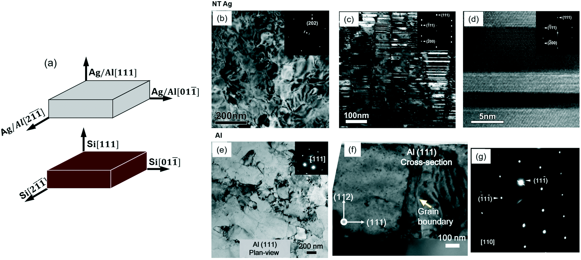 | ||
| Fig. 1 Epitaxial nanotwinned (NT) Ag (111) and Al (111) films: (a) orientation relationship of the films with respect to Si (111) substrate. (b and e) Plan-view TEM micrographs showing single-crystal like films in Ag and Al films. (c and f) Cross-section TEM (XTEM) micrographs of NT Ag and Al examined from the <110> zone axis showing that Ag has high-density nanotwins and columnar grain boundaries, whereas Al has few twin structures and coarse grains. (d) High-resolution TEM micrograph showing coherent twin boundaries oriented perpendicular to the growth direction in Ag. (g) Selected area diffraction pattern (SAED) of Al indicating single-crystal like structure from <110> direction. Figures were adapted with permission from ref. 33 and 34. | ||
2.2 SFE effect
The drastically different twinning propensity in Ag and Al prepared using similar synthetic conditions is attributed to their difference in SFE. The SFE is the energy penalty for the SF formation between two adjacent slip planes through relative shear. Since the consecutive SFs along adjacent planes result in the formation of twin embryo, the SFE plays a critical role on the twin formation.36 A few methods have been developed to interpret the twinnability, considering the relative energy discrepancy among the fault energies. In general, there are four fault energies controlling the twin formation via the slip of Shockley partials on {111} planes along <112> direction in FCC metals. First, according to the generalized planar fault energy curve, unstable SFE (γUSFE) is the energy barrier for slip of a partial dislocation to generate a SF. When γUSFE is overcome, the dislocation moves to a local energy-minimal position, i.e. the stable SFE (γSFE). To form a twin embryo containing two consecutive SFs, the unstable twin fault energy (γUTF) needs to be conquered to reach another energy-minimal state, referred to as twin fault energy (γTF). Van Swygenhoven et al. implemented molecular dynamics simulations to show that the ratios of γUSFE/γSFE and γUTF/γTF decide the probability for the formation of SFs and TBs instead of γSFE alone.37 Bernstein et al. calculated the ratio of critical stress intensity factors for twin growth and annihilation in FCC metals.38 When the ratio is greater than 1, twinning is favored and the expression can be simplified as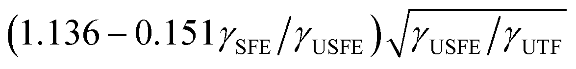 , suggesting that low ratios of γSFE/γUSFE and γUTF/γUSFE favor the twinning. For example, the ratios of γSFE/γUSFE for Al, Ni, and Cu are 0.97, 0.55, and 0.13 respectively, indicating that Al is energetically unfavorable for twin formations and would more readily undergo detwinning process, whereas Cu has a higher possibility to form stable twins. Moreover, Wu et al. identified a softening phenomenon as twin spacing falls below a threshold value, for which the migration, i.e. detwinning, of CTB kinks and steps that act as easier dislocation nucleation sites is responsible.39 As a result, detwinning tends to occur for thin twins. Through various topological analyses and atomic simulations, Wang et al. investigated the detwinning mechanisms of NT metals with different SFEs. Specifically, for FCC metals with comparably low SFEs, such as Ag and Cu, detwinning takes place through the collective glide of partials, referred to as the phase-boundary-migration mechanism. On the other hand, for FCC metals with high SFEs, such as Al, detwinning occurs through both migration and sliding via the glide of interface disconnection, referred to as the interface-disconnection-glide mechanism.40–42 Alloying could potentially alter the energy landscape. Schulthess et al. used self-consistent electronic structure calculations and found that Mg addition could reduce the SFE of Al under a chemically disordered solid solution condition, while Cu and Ag increase the SFEs.43 Li et al. showed that adding Fe to Al could increase the energy barrier for detwinning despite the slight increase of absolute SFE.35 Meanwhile, alloying could also introduce solute segregation at TBs to influence twin mobility.12
3. Synthesis techniques and conditions for twin formation in epitaxial NT metals
3.1 Effects of deposition rate and temperature
A majority of epitaxial NT metals have been synthesized by sputtering depositions wherein ionized inert gas molecules are accelerated under potential to bombard the target materials and eventually deposit the ejected atoms and/or their clusters onto the anode (substrate) in high vacuum. This process renders well-defined orientation of epitaxial film with respect to the crystallographic orientation of the substrate. Moreover, sputtering technique can control the purity and compositions of the films. The intrinsic microstructure of sputter-deposited materials can be influenced by various external factors, such as deposition power, substrate temperature and bias etc. Anderoglu et al. showed that the twin spacing in epitaxial NT Cu can be reduced from 16 to 7 nm as the deposition rate increased from 0.9 to 4 nm s−1.13,44 A thermodynamic vapor nucleation model was used to analyze the critical radius difference between perfect nucleus and twin nucleus.18 The model shows that low TB energy and high deposition rate favor the twin formation. However, increasing the deposition rate changes negligibly the critical radius difference between perfect and twinned nuclei for metals with low SFE.33 Ott et al. revealed that the twin spacing of NT Ag with a SFE of 17 mJ m−2 varies slightly from 12 nm to 8 nm when the deposition rate increases from 1.5 to 5.4 nm s−1.45In addition, the model suggests that deposition rate alone is insufficient to increase twin density in high-SFE metals. Sputtered NT Ni with an SFE of 120–130 mJ m−2 exhibited a twin spacing of 182 nm. Xue et al. further modified the aforementioned thermodynamic model and showed that the nucleus radius of nanotwins in Al with a high SFE of 120–144 mJ m−2 is at least 25% greater than that of perfect nucleus at a very high deposition rate, and yet it remains challenging to introduce growth twins in Al.46 Dahlgren et al. discovered that sputtering Ni at −150 °C and at a high deposition rate of 12.5–30 nm s−1 could generate nanotwins, but depositions at elevated temperatures gave rise to coarse twins, suggesting the temperature effect on the formation of growth twins.47 Interestingly, Velasco and Hodge tested temperature-dependent twin spacing of various sputtered NT Cu–Al and Cu–Ni alloys and showed that when SFE is 37–60 mJ m−2, sputtering at elevated temperatures led to thicker growth twins.48 However, they found that in NT Cu–4 wt% Al or Cu–6 wt% Al alloys, finer twin structures were attained through high temperature (250–350 °C) depositions. They attributed this intriguing observation to the high twin nucleation rate and the Zener drag effect of the alloying elements on twin growth. It is worth noting that for NT Cu alloys with low SFE (<15 mJ m−2), the dependence of twin thickness on substrate temperature becomes insignificant in general. The diffusion and interactions of solute and matrix atoms become sensitive to substrate temperature, and make the interpretation of temperature-dependent formation of growth twins more complex.
3.2 Electrodeposition vs. sputtering
We now turn our attention to electrodeposition, a high-rate growth technique that has been widely used by the coating industry. Scientific communities have paid more attention to this technique due to its ability to synthesize NC materials as well as the discovery of polycrystalline NT Cu with high strength at little expense of ductility and electric conductivity.4,11,49,50 To date, a majority of electrodeposited NT metals and alloys are polycrystalline. Current density is a significant parameter to control the nucleation rate and thus the twin spacing. Lu et al. showed increasing average current density from 70 to 300 mA cm−2 (using pulsed DC electrodeposition) could increase deposition rate from 2.6 to 10 nm s−1, and reduces the twin spacing of NT Cu from 15 to 4 nm.11 Many tunable parametric factors in the electrodeposition could affect the twin attributes. Hasegawa et al. unveiled that the texture and twin orientation showed a dependence on the deposition potential. Horizontal nanotwins formed in pulse electrodeposited NT Cu at an on-potential of −0.2 V vs. saturated calomel electrode (SCE), whereas inclined nanotwins were attained at −0.6 V.51,52 Chan et al. tailored the chloride concentration from 10−4 to 10−5 M in order to change the Cu texture from (111) to (110). They ascribed the crystallographic texture evolution to the Cl− effect on cathodic overpotential and deposition rate, which affected the time for Cu adatoms to reach and desorb from different crystallographic planes with different exchange current densities.53 However, it was speculated in general that metals would be hardly epitaxially grown in the high-flux electrodeposition conditions. Several studies showed that using an optimum stirring speed, current density and a Cu seed layer amid electrodeposition processes could synthesize NT Cu with horizontal twins and a strong (111) texture.19,54,55 Likewise, by applying stirring during the electrodeposition, similar NT Cu was able to grow on Ti substrate.56,57 Chen et al. showed that the programmable waveforms, i.e. pulse electrodeposition, played more profound roles in making NT Cu, considering that direct-current (DC) rendered a transition layer of more randomly oriented grains at film–substrate interface, notwithstanding the optimal electroplating conditions.58Various studies showed that nanotwins can be synthesized in polycrystalline Ni via electrodeposition.59–61 The question here is whether electrodeposition can lead to the deposition of single-crystal-like or highly textured NT high-SFE metals? Li et al.29 used a hybrid sputtering–electrodeposition technique to demonstrate the success in deposition of epitaxial NT metals. Using magnetron sputtering, they first deposited an epitaxial NT Cu (111) seed layer on Si (110) substrate, and then they compared the microstructure of electrodeposited Ni and sputtered Ni using the same seed layer as illustrated in Fig. 2a. The ion beam channeling image in Fig. 2b and the automated crystal orientation map (ACOM) in Fig. 2c show that the sputtered Ni possesses thick twins with an average twin spacing of 182 ± 118 nm. In comparison, the electrodeposited Ni using an organic additive generated epitaxial NT Ni consisting of a unique TB network: high-density horizontal CTBs and vertical ITB segment as shown in Fig. 2d and e. A unique character of the electrodeposited NT Ni is the giant grain size with few conventional GBs. Cross-sectional TEM micrographs in Fig. 2f and g suggest that the fine nanotwins have an average twin spacing of 22 nm in epitaxial Ni (111) and the TBs have abundant steps, kinks and SFs. The additive hypothetically allowed a transfer of the growth mode from a 3D cluster growth to a quasi-2D layer-by-layer growth and facilitated twin nucleation.
 | ||
| Fig. 2 Single-crystal-like NT Ni prepared by electrodeposition on sputtered NT Cu (111) template on Si substrate. (a) Two routes to grow NT Ni: (I) sputtering of Cu and then Ni, (II) sputtering of NT Cu followed by electrodeposition of NT Ni. (b and d) Cross-section ion channeling images and (c and e) automated crystal orientation maps (ACOM) of Ni prepared by two routes. The sputtering/electrodeposition route introduces very large grain size and small twin spacing in NT Ni. (f) XTEM micrograph showing high-density growth twins with heterogeneous twin thickness. (g) HRTEM micrograph showing incoherent twin boundaries (ITBs), kinks and SFs on coherent twin boundaries (CTBs). Figures were adapted with permission from ref. 29. | ||
We notice that the reports on twin formation in electrodeposited Al and Pd (130–180 mJ m−2) are rare partially because of their high SFEs.62 Al and Pd have high γSFE/γUSFE ratio, suggesting their low twinnability.38 In spite of a more negative reduction potential of Al3+, i.e. −1.68 V versus standard hydrogen electrode (SHE), researchers managed to electrodeposit Al and its alloys using ionic liquids as electrolytes.63,64 In a recent work, Rafailovic et al. grew 10 μm-thick Al electrodeposits onto Ag seed layer and found that nanoscale inclined twins nucleated at sites distant from Al/Ag interface and few twins were spotted at the epitaxial region in the vicinity of the interface.65 The authors proposed that the adsorbed hydrogen layer on Al amid the growth facilitated the nucleation of twins. These studies strongly imply that a non-equilibrium, high-flux process does not necessitate the twin formation, but the interfacial electrodeposit/electrolyte reaction may be critical for the twin formation.
4. Alloying effect on formation of growth twins
4.1 Low- and intermediate-SFE metals
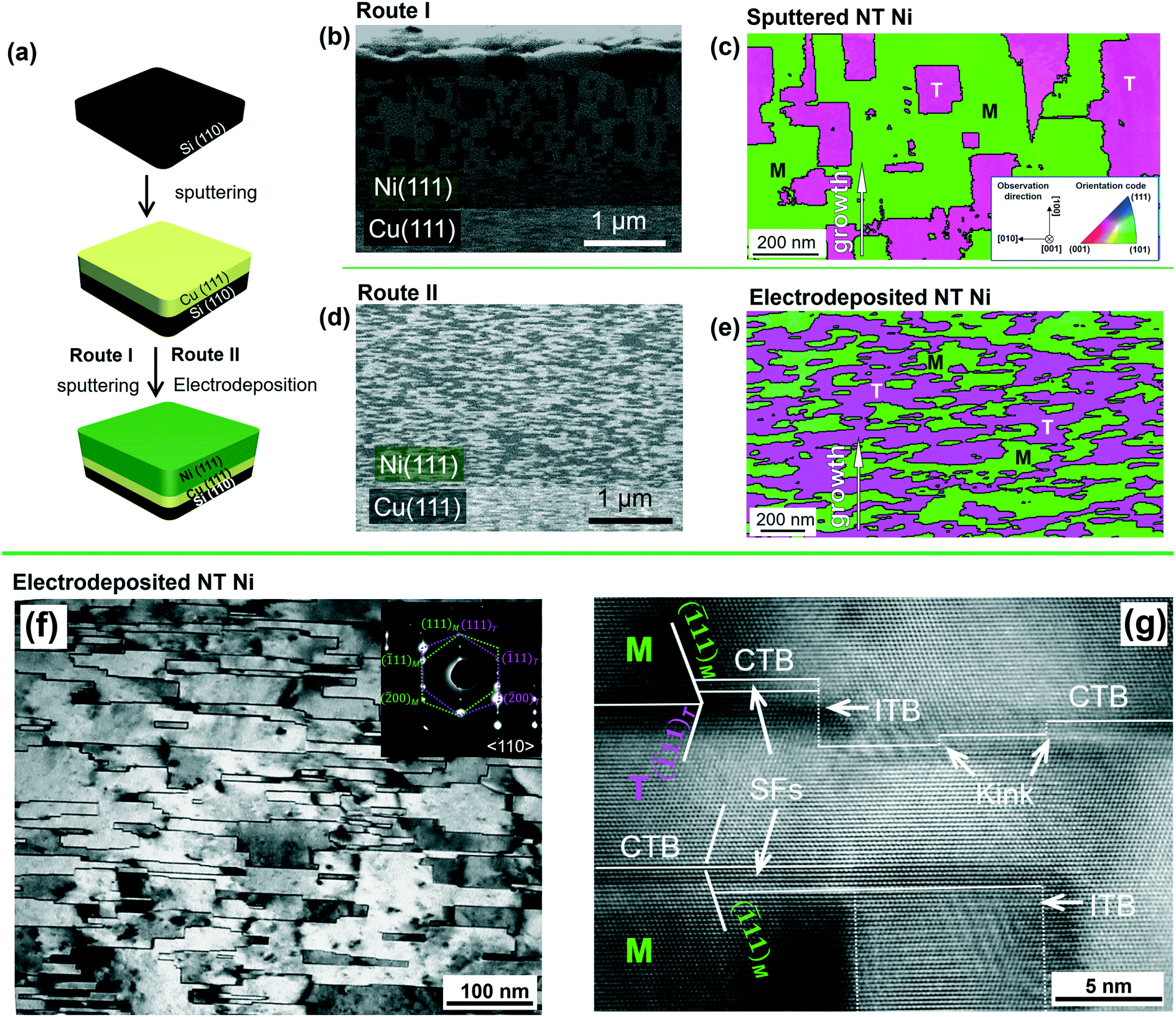
Fan et al. used magnetron sputtering to grow epitaxial NT Cu (111) on Si (110)66 as evidenced by the XRD profile in Fig. 3a. The ϕ scan in Fig. 3b shows identical diffraction peaks from twins and matrices, indicating the formation of growth twins in Cu film. The corresponding film–substrate orientation relation is (01)Cu//(10)Si, [![[2 with combining macron]](https://www.rsc.org/images/entities/char_0032_0304.gif) 11]Cu//[001]Si as illustrated in Fig. 3c. XTEM micrographs (Fig. 3d and e) show that columnar grains, ∼100 nm in diameter, were filled with fine twins with an average twin spacing of 8 nm. Furthermore, the plan-view TEM micrograph in Fig. 3f shows that the columnar boundaries were decorated with nanovoids. Fan et al. in a separate study found alloying NT Cu with 3 at% Fe increased the average twin spacing to 14 nm.67 Velasco et al. have sputtered NT Cu–Al and Cu–Ni alloys at different deposition rates and temperatures,48 and found that the average twin spacing of NT Cu could be reduced from 8 to 5 nm by alloying with Al as shown in Fig. 3h–j.
11]Cu//[001]Si as illustrated in Fig. 3c. XTEM micrographs (Fig. 3d and e) show that columnar grains, ∼100 nm in diameter, were filled with fine twins with an average twin spacing of 8 nm. Furthermore, the plan-view TEM micrograph in Fig. 3f shows that the columnar boundaries were decorated with nanovoids. Fan et al. in a separate study found alloying NT Cu with 3 at% Fe increased the average twin spacing to 14 nm.67 Velasco et al. have sputtered NT Cu–Al and Cu–Ni alloys at different deposition rates and temperatures,48 and found that the average twin spacing of NT Cu could be reduced from 8 to 5 nm by alloying with Al as shown in Fig. 3h–j.
 | ||
| Fig. 3 Epitaxial NT Cu, Cu97Fe3 and Cu–Al alloys with various compositions, grown on Si (110) substrates. (a) XRD profile, (b) phi-scan profile, showing six-fold symmetry suggestive of significant twin formation. M and T denote matrix and twin peaks, respectively. (c) The orientation relation of films with Si (111) substrate for NT Cu. (d and e) XTEM micrographs showing nanotwins in epitaxial NT Cu. (f) Plan-view TEM micrograph showing epitaxial NT Cu with nanovoids. (g–j) XTEM micrographs of NT Cu97Fe3, Cu95.4Al4.6, Cu91Al9 and Cu87Al13 alloys showing alloying effects on twin spacing. Figures were adapted with permission from ref. 48, 66 and 67. | ||
The alloying effects on twin spacing can be understood partially by considering the SFE effect. Alloying elements can influence SFE in a parental metal. Stable SFE as an intrinsic property can be experimentally measured, but the values were scattered. First-principle calculation has been broadly adopted to depict the SFEs in order to understand the alloying effect on twinnability. Li et al. calculated the SFEs of binary Cu–X (X = Al, Zn, Ga or Ni) and found that Al, Zn and Ga additions reduced the SFEs, whereas Ni has the opposite effect.68 Likewise, Kibey et al. revealed that increasing Al boosted the twinnability in Cu.69 Shao et al. further investigated the influence of a variety of substitutional and interstitial solutes on twinning tendency and revealed that Sn, Al, Zn, Si, Ge, P, C, N and O could reduce the SFE of Cu with different effectiveness.70 For this reason, Velasco et al. found that Al and Ni could affect twin spacing differently in Cu (ref. 48) and Fan et al. found Fe solutes increased the twin spacing in NT Cu.67 Alloying effect was proven effective to change twin density in Ni. Sim et al. reported that sputtered NT Ni–Mo–W has an average twin spacing of several nanometers.32 Bahena et al. found that the sputtered Inconel 725 Ni-based superalloy has columnar grains with nanotwins.71 These alloying elements significantly decreased the SFEs of Ni. Shang et al. concluded that 26 alloying elements decreased the SFE of Ni in their first-principle calculation study.72
4.2 High-SFE metals
A distinct microstructure of growth twins has been reported in Al and its alloys with high SFEs. In comparison to the single crystal Al (111) (Fig. 4a) with a grain size of 500 nm,35 the sputtered Al–2.5 at%Fe film in Fig. 4b shows evident grain refinement, and the three extra spots on the outer peripheral of XRD pole figure indicate the formation of growth twins. High density growth twins were also observed in sputtered Al–5.5 at%Fe (Fig. 4c). A majority of TBs in Al–Fe alloys are ITBs with diffuse characteristics, i.e., 9R phase. Similar columnar microstructures with ITBs have been observed in sputtered Al–Ti,74 Al–Mg (ref. 34) and Al–Ni,73 as shown in Fig. 4d–f, although the solutes have different extent of impact in grain refinement, an aspect to be elucidated subsequently.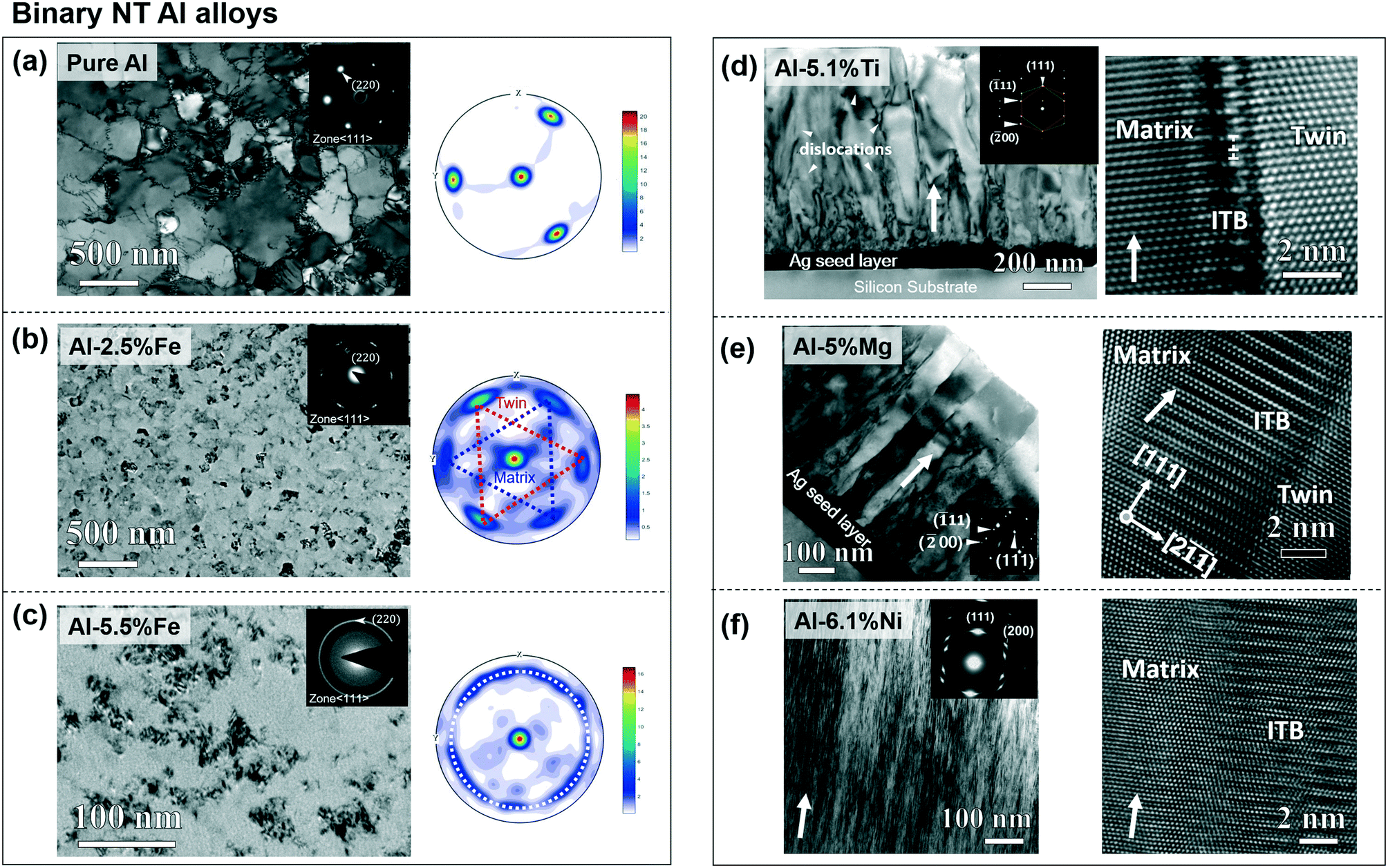 | ||
| Fig. 4 NT Al binary alloys on Si (111) substrates. (a) Plan-view TEM micrograph and X-ray pole figure of pure Al (111) without twins. (b) TEM micrograph of Al97.5Fe2.5 showing nanograins and pole figure indicating abundant twin boundaries. (c) TEM diffraction pattern and pole figure of Al94.5Fe5.5 alloys showing nanograins with in-plane rotation. (d) XTEM micrograph of Al94.9Ti5.1 showing single crystal like film with nanotwins (indicated by the inserted SAD pattern). HRTEM micrograph showing ITBs. (e) XTEM micrograph of single-crystal-like NT Al95Mg5 with broad ITBs. (f) XTEM micrograph of highly textured NT Al93.9Ni6.1 alloys with distorted ITBs. Figures were cited and adapted with permission from ref. 34, 35, 73 and 74. | ||
Fe was proven effective experimentally in reducing ITB spacing and grain size, though density-functional theory (DFT) calculations showed that Fe solutes increase the SFE of the binary Al alloys.35 Li et al. also showed that the nanograins and ITBs in NT Al–Fe were stable up to 280 °C.75 The nanograins and small ITB spacing formed by the non-equilibrium process do not readily coarsen as a result of a large kinetic energy barrier. Meanwhile, Ni and Co presented comparable effectiveness in grain refinement in binary NT Al alloys (Fig. 4), but DFT calculations showed that these solutes reduce the SFE of Al.73,76 This difference in solute effect on adjusting SFE of Al indicates that twin formations in Al alloys may be kinetically controlled. We speculate that the impurity atoms pin the island growth and the Al alloys tend to reduce the excess elastic strain energy, stemming from the supersaturated solid solution, by creating abundant ITBs and low-angle GBs.9 Kube et al. stated that an optimal solute saturation and a corresponding GB area are correlated, and a larger GB area is required responding to the increase in solute concentration.77,78 Interestingly, Cr solutes having a comparable atom radius as Fe generate evidently greater grain size in binary Al–Cr alloys than Al–Fe alloy, and Cr segregates to GBs to alleviate excess free energy.79
5. Twin promotion via seed layer
For high-SFE Al, twin formation could also be promoted by introducing seed layers. Bufford et al. used Ag as a twinned seed layer to grow twins in Al.80Fig. 5 shows three mechanisms of the twin formation, supported by TEM evidence. For scenario one (Fig. 5a and a′), an ITB nucleated from Ag seed layer can extend into Al film. Likewise, in scenario two, a parallel CTB in Ag can propagate into Al with the assistance of the curvature at Al/Ag interface (Fig. 5b and b′). Different from the TB extension across Al/Ag interface, scenario three in Fig. 5c and c′ suggests that adjacent to the interface, SFs in Ag disturbed the stacking sequence of Al and stimulated the formation of ITB and CTB in Al. During the film growth process, the accumulation of ITB length would drastically increase the system energy as a result of the high ITB energy, 223–357 mJ m−2 in comparison with the CTB energy of ∼75 mJ m−2 for Al.40 A CTB eventually form so as to terminate the growth of ITB.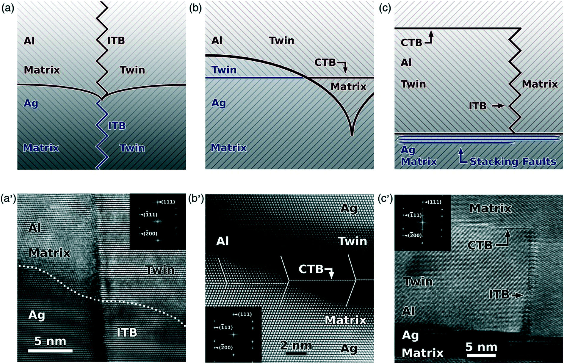 | ||
| Fig. 5 Schematics and HRTEM images showing three mechanisms of twin formation mechanisms in epitaxial twinned Al deposited on NT Ag seed layers. (a and a′) ITB propagation from NT Ag into Al. (b and b′) Lateral extension of CTB from Ag into Al through coherent Ag/Al layer interfaces. (c and c′) ITB nucleation from high-density SFs at the Ag/Al interface. Figures were cited with permission from ref. 80. | ||
To make sure that the TBs from the seed layer is inherited by the films, the epitaxial growth criteria ought to be fulfilled. In case of a small mismatch strain, the film could maintain the epitaxial growth from the seed layer template over extended thickness. The mismatch strain between Ag and Al is 0.9%, ensuring a coherency at the interface and thus promoting twin propagation into Al with different mechanisms.33,80
The twin formations were also reported in multilayer systems. One twin formation mechanism in the nanolaminate systems is similar to the seed layer method, which utilizes the twin replication mechanism across the coherent interface between a low-SFE metal and a high-SFE metal.80–83 The second twin formation mechanism is the interlayer-interruption-growth method. When a heterogeneous layer is deposited, the regular stacking sequence can be altered and SFs can be introduced. The introduction of SFs might trigger the twin formation.80,81,84
6. Texture effect
In a different strategy, the texture of epitaxial Al films gives rise to different twin density and morphology, controlled by the Si substrates.85Fig. 6 shows the epitaxial growths of NT Al (111), (110) and (112) on Si (111), (110) and (112), respectively. When Al grew on Si (111) substrate, the adatom clusters have two possible orientations with a relative 60° in-plane rotation with respect to the out-of-plane [111] direction. Coincidently, these two domains have a twin relationship (Fig. 6a). Hence, their impingements generated vertical ITBs, validated by TEM experiments (Fig. 6b). The purple and pink colors represent the matrix and twin domains, respectively, in the orientation mapping collected using a transmission Kikuchi diffraction (TKD) technique (Fig. 6c) and domain boundaries are vertical ITBs. In Al (110), CTBs are inclined at 35° relative to Al/Si interface as illustrated in Fig. 6d, validated experimentally in Fig. 6e and f. It should be noted that due to the texture and a large discrepancy of lattice parameter between Si (110) and Al (110), various types of twin formations were observed and we direct the audience to the literature for more details.85 In the third case, the Al grown on Si (112) has a dominant (112) orientation despite an approximate 4° misorientation between Si (112) and Al (112) (Fig. 6g). The (112) and (212)-oriented domains give rise to ITBs that have a 15° rotation compared to the vertical ITBs of Al (111), shown in Fig. 6h. It was noticed that Al (112) had the highest twin density when compared to Al (111) and (110). Xue et al. believe that the crystal irregularity, i.e. (102) crystallite in Al (112) (Fig. 6i), acted as a barrier to inhibit the excessive growth of (112) or (212) domains, promoting a higher density of TBs. In the orientation-directed mechanism of twin formations, twins could form with different propensity and morphology in high-SFE Al by tuning the Si substrate orientation.85 Certain substrate texture could promote the differently oriented twin nuclei at the early stage of thin film growth. As the twin nuclei grow and impinge each other, a TB forms to reduce the surface energy.42 The dihedral angle between TB and substrate surface varies with the crystal orientation of the films, lending opportunity to tailor the twin morphology.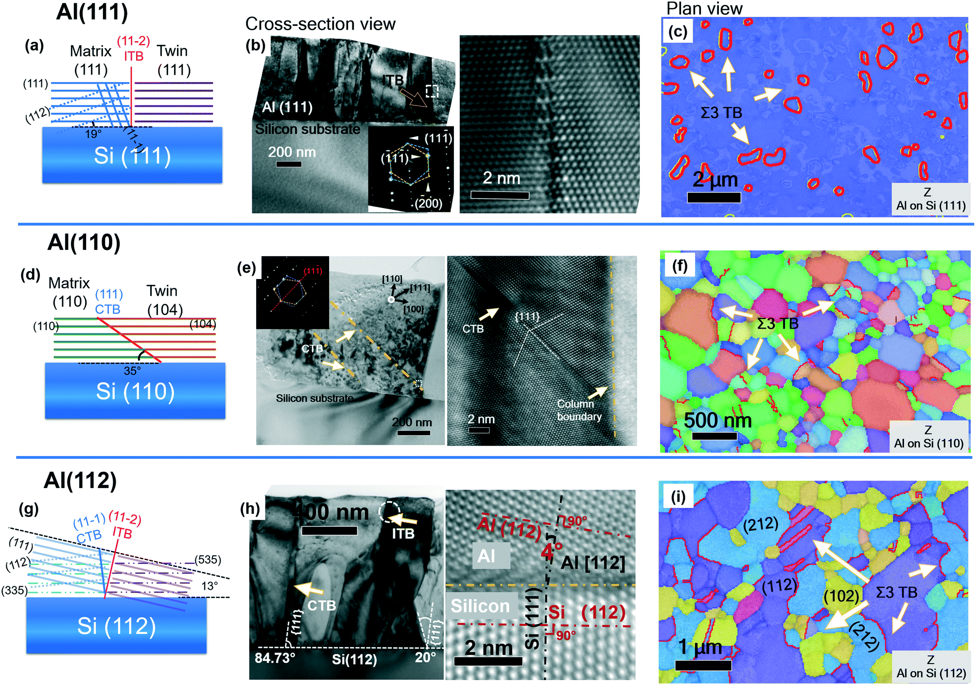 | ||
| Fig. 6 Twin morphologies and propensity of growth twins in Al with (111), (110) and (112) textures deposited on various types of Si substrates. (a, d and g) Orientation relationship of twin structures in three types of textured Al films, (b, e and h) XTEM micrographs showing TBs oriented at different angles with respect to the growth direction depending on the type of Si substrates. (c, f and i) Plan-view inverse pole figure maps for Al (111), Al (110) and Al (112). Figures were adapted with permission from ref. 85. | ||
7. Various properties of epitaxial NT metals and alloys
7.1 Intrinsic size effect on strength
It is well-known that TBs strengthen the NT metals by acting as barriers to dislocation slips. Consequently an “intrinsic size effect” has been established, that is, a smaller twin spacing renders a higher yield strength, as depicted by the Hall–Petch relationship revealing a nearly linear relation between the mechanical strength and the reciprocal square root of the twin spacing.1–3 Interestingly, Kini et al. studied the mechanical response of NT Ag with a wide spectrum of twin spacing from 1.8 μm to 15 nm under microcompression.87 The stress–strain curves of NT Ag compressed parallel to CTBs in Fig. 7a suggests that the flow stress increases with the decreasing twin spacing. They fit the data to the power law-type relation and found out a twin spacing scaling exponent approaching unity, suggesting the dislocation curvature related deformation mechanism, namely the confined layer slip mode.88 Anderoglu et al. showed that decrease in twin spacing of epitaxial NT Cu from 16 nm to 7 nm increase the hardness from 2.1 GPa to 2.8 GPa.44 Zhang et al. and Hodge et al. showed that NT Cu with ∼5 nm and 40–80 nm twin spacing rendered a tensile strength of 1.2 GPa and ∼550 MPa, respectively.17,89 Heckman et al. reported that epitaxial NT Cu alloys' mechanical strength is affected by both twin spacing and columnar grain width and a transition from shift from slip band or detwinning-controlled mechanisms to intergranular fracture would occur as the twin spacing falls below ∼30 nm.90 The engineering stress–strain curves of micropillar compression tests in Fig. 7b show that NT Al–Fe is much stronger that NT Al–Mg. As shown in Fig. 7c and d, Ni, Fe and Co are more effective than Ti, Zr and Mg in reducing the average grain size and twin spacing of Al.34,35,73,74,76,86 Consequently, the NT Al–Fe, Al–Ni and Al–Co alloys have high indentation hardnesses (Fig. 7e), exceeding 5.5 GPa.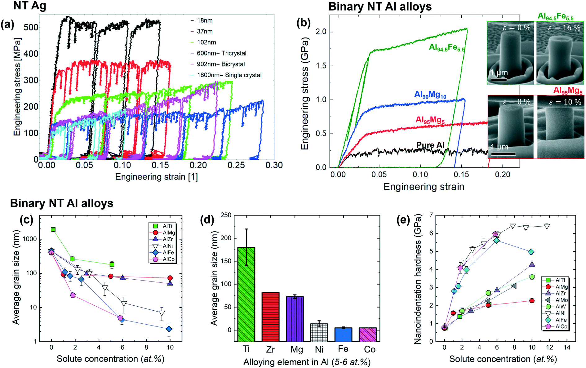 | ||
| Fig. 7 Mechanical behaviors of NT Ag and binary NT Al alloys. (a) Representative engineering stress–strain curves for Ag with varying twin spacing, collected via micropillar compression tests, showing smaller twin structures rendering higher strength. (b) Engineering stress–strain curves for pure Al, Al–Mg and Al–Fe alloys showing that strength increases with the decreasing twin spacing. (c) Average grain size of binary NT Al alloys decreases with the increasing solute concentration. (d) Alloying elements with 5–6 at% compositions have variable effectiveness in grain refinement. (e) Nanoindentation hardness versus solute concentration for various binary NT Al alloys. Figures were cited and adapted with permission from ref. 34, 35, 73, 74, 76, 86 and 87. | ||
7.2 Electrical conductivity
In conventional metals with high-angle GBs, grain refinement leads to high mechanical strength, but significantly degrades the electrical conductivity, because high angle GBs significantly scatter free electrons. Anderoglu et al. showed that the upper bound of electrical resistivity coefficient of CTBs in Cu is 1.5–5 × 10⁻⁷ μΩ cm2, approximately an order of magnitude lower than that of high-angle GBs.13,44 They varied the sputtering deposition rate to synthesize epitaxial NT Cu films with average twin spacing varying from 16 to 7 nm. Their study (Fig. 8a) shows the room temperature resistivities of epitaxial NT Cu are within the range of 1.69–2.31 μΩ cm2, approaching the resistivity of oxygen-free high-conductivity Cu, 1.58 μΩ cm2, much less than the high resistivity of NC Cu, 19 μΩ cm2.3,4 Xing et al. recently summarized the relations between the yield strength/shear modulus, σy/μ, and electrical conductivity of various nanometals and alloys and found that metals with TBs inside NC grains have an exceptional combination of strength and electrical conductivity and do not comply with the relation of inversely correlated strength–electrical conductivity.3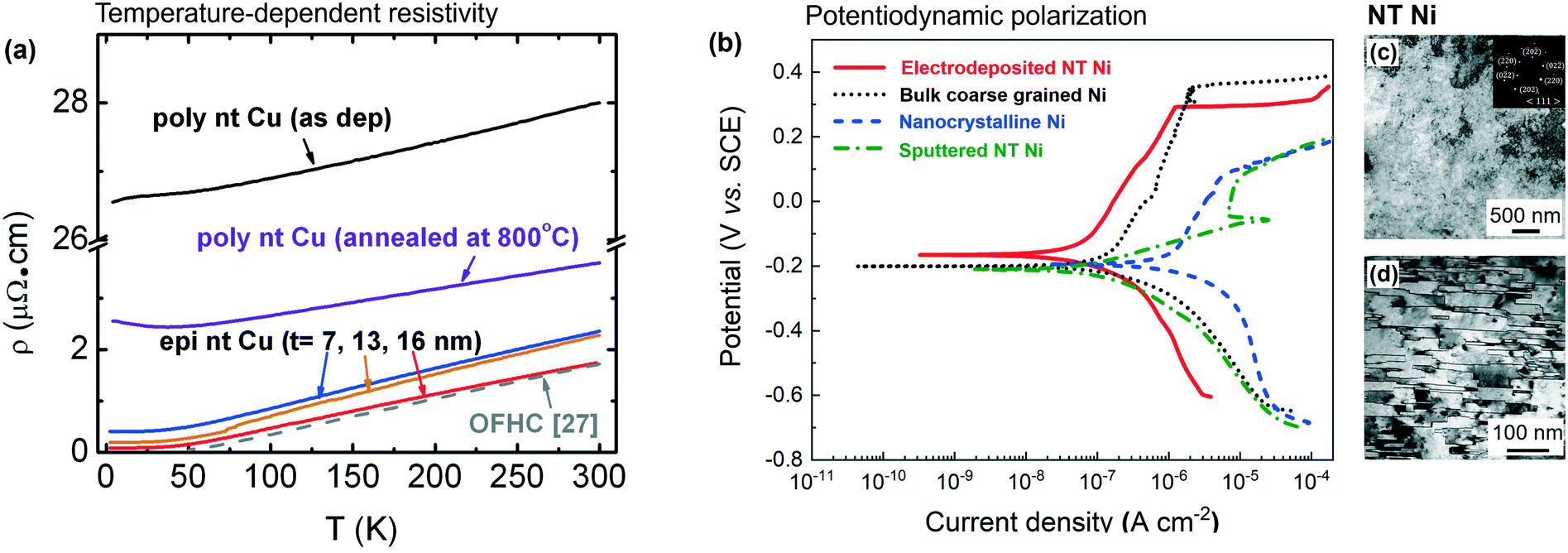 | ||
| Fig. 8 Electric conductivity of NT Cu and corrosive behaviors of NT Ni. (a) Comparison of temperature-dependent resistivity measurements of polycrystalline and epitaxial NT Cu films. Larger average twin spacing led to lower resistivity of epitaxial NT Cu films. (b) Potentiodynamic polarization curves for bulk coarse-grained, NC, sputtered NT and electrodeposited Ni in artificial seawater. (c) Plan-view and (d) cross-section TEM micrographs of electrodeposited NT Ni show high-density stepped TBs and few conventional columnar grain boundaries. Figures were cited and adapted with permission from ref. 29 and 44. | ||
7.3 Corrosion behaviors
It has been widely shown that high-angle GBs are active sites for corrosion attacks.27,28,91 Watanabe introduced the concept of “grain boundary design and control” pertaining to the GB characters, particularly coincidence site lattice (CSL) boundaries that cause difference in intergranular fracture.92 Meanwhile it has been long proposed that low ∑CSL boundaries, such as ∑3 TBs, may have better resistance to localized corrosion attacks than conventional high-angle GBs.93 Michiuchi et al. show that 316 austenitic stainless steel with 86% CSL boundaries alleviated intergranular corrosion amid the ferric sulfate–sulfuric acid tests, partially contributing to the TB-associated GB engineering.94 Recent scattered studies showed that nanotwins in equiaxed grains could help form thin and continuous passive layers to enhance corrosion resistance. Meng et al. has electrodeposited NC Ni containing nanoscale twins91 and Li et al. synthesized nanostructured 316L austenitic stainless steel consisting of twin bundles by dynamic plastic deformation.95 They found that the corrosion resistance of NT metallic materials was improved compared with that of the cast and the matrix counterparts. TBs serve as nucleation sites that enhance the spontaneous passivation and lead to a higher growth rate of the passive layers.To date, there are few investigations on corrosion response of epitaxial NT metals. Hodge et al. showed that epitaxial NT Cu had improved pitting resistance and more stale passive layers when compared to other NT Cu with lower twin fractions and coarse-grained Cu.30 The protective passive layer was ascribed to a preferential formation of {111} Cu2O on the NT Cu with a strong (111) texture. Moreover, according to the aforementioned, low-angle GBs theoretically are less vulnerable to corrosion attacks. In the NT Cu, the preferential corrosive attacks may initiate through the columnar ITBs in most cases, but the intergranular corrosion is likely arrested once in encounters the low-energy CTBs. Li et al. compared the corrosion resistance of two types of epitaxial NT Ni to coarse-grained Ni and NC Ni. As shown in Fig. 8b and Table 1, the sputter-deposited epitaxial NT Ni has lower corrosion rate and corrosion current than coarse-grained Ni and NC Ni, but lacks passivation. The long ITB segments intersecting with free surface in sputtered NT Ni (Fig. 2c) caused an uninterrupted invasion of corrosion and lowered the pitting resistance.29 In contrast, the electro-deposited NT Ni has the highest corrosive potential, polarization resistance and lowest corrosion rate among differently microstructurally constructed Ni. The electrodeposited epitaxial NT Ni has short ITB segments that terminate at the free surface (Fig. 2d–g) and the corrosion path would be quickly arrested at the ITB–CTB junctions. Its hierarchical networks of CTB and ITB segments are effective in arresting corrosion propagation and facilitating the fast diffusion of Ni ions for the formation of passive layer.
| Specimen name | E corr (mV) | i corr (A cm−2) | R p (kΩ) | V corr (milli-inch per year) |
|---|---|---|---|---|
| Note: Ecorr, icorr, Rp and Vcorr are corrosive potential, corrosive current density, polarization resistance and corrosion rate, respectively.29 | ||||
| Bulk coarse grained Ni | −200 | 1.59 × 10⁻⁷ | 202 | 64 × 10−3 |
| Nanocrystalline Ni | −192 | 1.24 × 10⁻⁶ | 24 | 502 × 10−3 |
| Sputtered NT Ni | −210 | 9.13 × 10⁻⁸ | 216 | 36 × 10−3 |
| Electrodeposited NT Ni | −166 | 6.91 × 10⁻⁸ | 516 | 28 × 10−3 |
8. Future outlooks
TBs have injected unique mechanical and physical properties, such as the concomitant superb strength/ductility/conductivity, to metallic materials. For epitaxial NT metals and alloys, future works should put more emphasis on the following issues, including, inter alia: (i) fundamental understanding of the alloying effects on the stability of twin structures as exposed to principal, complex stresses and elevated temperature; (ii) new synthetic avenues and parametric control for the fabrication of epitaxial NT metals, such as the electrodeposit/electrolyte reactions and usage of buffer/seed layers; (iii) experimental and theoretical studies towards high-SFE metals and alloys; (iv) construction of TB networks to achieve desirable mechanical, physical and chemical properties, in comparison to conventional GBs; (v) scale-up of epitaxial NT metals for practical applications. Limited efforts have been spent on applying NT materials. By far, we saw epitaxial or highly textured NT metals and alloys have been proposed to be utilized in applications, including integrated-circuit packaging,19 3D printing for sensors and plasmonics,31 and microelectromechanical systems (MEMS).329. Conclusion
In summary, the review focuses on the epitaxial NT metals and alloys with both low and high SFEs and demonstrates the dependence of twin structures and their properties on the extrinsic factors, such as the synthesis technique, parametric control, texture and seed layer, as well as the intrinsic factors including the composition and SFE. The followings briefly summarize the major findings in this subject in recent years.(i) Vapor-based techniques can effectively tune the twin density of low-SFE NT metals and alloys by varying deposition rate and temperature. The texture control through the use of template and seed layer can change the twin density and morphology.
(ii) Alloying is a highly effective approach in tailoring the twin spacing both thermodynamically and kinetically via altering the SFE, the growth kinetics and twin stability, and eventually affects the mechanical properties of NT metals.
(iii) Epitaxial NT metals have unique TB network, distinct from NC and polycrystalline NT counterparts with conventional high angle GBs, and enable outstanding mechanical, physical and corrosive behaviors.
(iv) High-rate electrodeposition technique is promising to synthesize both low- and high-SFE epitaxial NT metals and alloys, and offers great opportunity to tailor twin structures via complex parameter control.
Conflicts of interest
There are no conflicts to declare.Acknowledgements
The works on NT Ni and Al alloys were supported by DoE-BES under grant no. DE-SC0016337. The works on NT Cu and its alloys were supported by NSF-CMMI-1728419. The authors also thank Dr. Daniel Bufford (Sandia National Laboratories) for the image contribution and discussion.References
- E. O. Hall, Proc. Phys. Soc., London, Sect. B, 1951, 64, 747–753 CrossRef.
- Z. C. Cordero, B. E. Knight and C. A. Schuh, Int. Mater. Rev., 2016, 61, 495–512 CrossRef CAS.
- X. Ke, J. C. Ye, Z. L. Pan, J. Geng, M. F. Besser, D. X. Qu, A. Caro, J. Marian, R. T. Ott, Y. M. Wang and F. Sansoz, Nat. Mater., 2019, 18, 1207 CrossRef CAS PubMed.
- L. Lu, Y. Shen, X. Chen, L. Qian and K. Lu, Science, 2004, 304, 422–426 CrossRef CAS.
- J. Schiotz and K. W. Jacobsen, Science, 2003, 301, 1357–1359 CrossRef CAS PubMed.
- V. Yamakov, D. Wolf, S. R. Phillpot, A. K. Mukherjee and H. Gleiter, Nat. Mater., 2004, 3, 43–47 CrossRef CAS PubMed.
- T. J. Rupert, D. S. Gianola, Y. Gan and K. J. Hemker, Science, 2009, 326, 1686–1690 CrossRef CAS PubMed.
- M. Legros, D. S. Gianola and K. J. Hemker, Acta Mater., 2008, 56, 3380–3393 CrossRef CAS.
- Q. Li, D. Y. Xie, Z. X. Shang, X. Sun, J. H. Cho, Y. F. Zhang, S. C. Xue, H. Y. Wang, J. Wang and X. H. Zhang, Acta Mater., 2020, 200, 378–388 CrossRef CAS.
- A. R. Kalidindi and C. A. Schuh, Acta Mater., 2017, 132, 128–137 CrossRef CAS.
- L. Lu, X. Chen, X. Huang and K. Lu, Science, 2009, 323, 607–610 CrossRef CAS PubMed.
- I. J. Beyerlein, X. H. Zhang and A. Misra, Annu. Rev. Mater. Res., 2014, 44, 329–363 CrossRef CAS.
- O. Anderoglu, A. Misra, H. Wang, F. Ronning, M. Hundley and X. Zhang, Appl. Phys. Lett., 2008, 93, 083108 CrossRef.
- S. Ogata, J. Li and S. Yip, Phys. Rev. B: Condens. Matter Mater. Phys., 2005, 71, 224102 CrossRef.
- Y. T. Zhu, J. Mater. Eng. Perform., 2005, 14, 467–472 CrossRef CAS.
- L. G. Sun, X. Q. He and J. Lu, npj Comput. Mater., 2018, 4, 6 CrossRef.
- X. Zhang, H. Wang, X. H. Chen, L. Lu, K. Lu, R. G. Hoagland and A. Misra, Appl. Phys. Lett., 2006, 88, 173116 CrossRef.
- X. Zhang, A. Misra, H. Wang, T. Shen, M. Nastasi, T. Mitchell, J. Hirth, R. Hoagland and J. Embury, Acta Mater., 2004, 52, 995–1002 CrossRef CAS.
- H. Y. Hsiao, C. M. Liu, H. W. Lin, T. C. Liu, C. L. Lu, Y. S. Huang, C. Chen and K. N. Tu, Science, 2012, 336, 1007–1010 CrossRef CAS.
- N. R. Tao and K. Lu, Scr. Mater., 2009, 60, 1039–1043 CrossRef CAS.
- S. Qu, X. H. An, H. J. Yang, C. X. Huang, G. Yang, Q. S. Zang, Z. G. Wang, S. D. Wu and Z. F. Zhang, Acta Mater., 2009, 57, 1586–1601 CrossRef CAS.
- J. Ding, Q. Li, J. Li, S. Xue, Z. Fan, H. Wang and X. Zhang, Acta Mater., 2018, 149, 57–67 CrossRef CAS.
- X. Li, Y. Wei, L. Lu, K. Lu and H. Gao, Nature, 2010, 464, 877 CrossRef CAS PubMed.
- L. L. Zhu, H. H. Ruan, X. Y. Li, M. Dao, H. J. Gao and J. Lu, Acta Mater., 2011, 59, 5544–5557 CrossRef CAS.
- E. Ma and T. Zhu, Mater. Today, 2017, 20, 323–331 CrossRef CAS.
- M. Dao, L. Lu, Y. F. Shen and S. Suresh, Acta Mater., 2006, 54, 5421–5432 CrossRef CAS.
- A. Chianpairot, G. Lothongkum, C. A. Schuh and Y. Boonyongmaneerat, Corros. Sci., 2011, 53, 1066–1071 CrossRef CAS.
- R. Mishra and R. Balasubramaniam, Corros. Sci., 2004, 46, 3019–3029 CrossRef CAS.
- Q. Li, S. C. Xue, P. Price, X. Sun, J. Ding, Z. X. Shang, Z. Fan, H. Wang, Y. F. Zhang, Y. X. Chen, H. Y. Wang, K. Hattar and X. H. Zhang, Nanoscale, 2020, 12, 1356–1365 RSC.
- Y. Zhao, I. C. Cheng, M. E. Kassner and A. M. Hodge, Acta Mater., 2014, 67, 181–188 CrossRef CAS.
- A. Behroozfar, S. Daryadel, S. R. Morsali, S. Moreno, M. Baniasadi, R. A. Bernal and M. Minary-Jolandan, Adv. Mater., 2018, 30, 1705107 CrossRef PubMed.
- G. D. Sim, J. A. Krogstad, K. M. Reddy, K. Y. Xie, G. M. Valentino, T. P. Weihs and K. J. Hemker, Sci. Adv., 2017, 3, e1700685 CrossRef PubMed.
- D. Bufford, H. Wang and X. Zhang, Acta Mater., 2011, 59, 93–101 CrossRef CAS.
- S. C. Xue, Q. Li, Z. Fan, H. Wang, Y. F. Zhang, J. Ding, H. Y. Wang and X. H. Zhang, J. Mater. Res., 2018, 33, 3739–3749 CrossRef CAS.
- Q. Li, S. C. Xue, J. Wang, S. Shao, A. H. Kwong, A. Giwa, Z. Fan, Y. Liu, Z. M. Qi, J. Ding, H. Wang, J. R. Greer, H. Y. Wang and X. H. Zhang, Adv. Mater., 2018, 30, 1704629 CrossRef PubMed.
- S. Ogata, J. Li and S. Yip, Science, 2002, 298, 807–811 CrossRef CAS PubMed.
- H. Van Swygenhoven, P. M. Derlet and A. G. Froseth, Nat. Mater., 2004, 3, 399–403 CrossRef CAS PubMed.
- N. Bernstein and E. B. Tadmor, Phys. Rev. B: Condens. Matter Mater. Phys., 2004, 69, 094116 CrossRef.
- Z. X. Wu, Y. W. Zhang and D. J. Srolovitz, Acta Mater., 2011, 59, 6890–6900 CrossRef CAS.
- J. Wang, A. Misra and J. P. Hirth, Phys. Rev. B: Condens. Matter Mater. Phys., 2011, 83, 064106 CrossRef.
- J. Wang, N. Li, O. Anderoglu, X. Zhang, A. Misra, J. Y. Huang and J. P. Hirth, Acta Mater., 2010, 58, 2262–2270 CrossRef CAS.
- J. Wang, O. Anderoglu, J. P. Hirth, A. Misra and X. Zhang, Appl. Phys. Lett., 2009, 95, 021908 CrossRef.
- T. C. Schulthess, P. E. A. Turchi, A. Gonis and T. G. Nieh, Acta Mater., 1998, 46, 2215–2221 CrossRef CAS.
- O. Anderoglu, A. Misra, F. Ronning, H. Wang and X. Zhang, J. Appl. Phys., 2009, 106, 024313 CrossRef.
- R. T. Ott, J. Geng, M. F. Besser, M. J. Kramer, Y. M. Wang, E. S. Park, R. LeSar and A. H. King, Acta Mater., 2015, 96, 378–389 CrossRef CAS.
- S. Xue, Z. Fan, Y. Chen, J. Li, H. Wang and X. Zhang, Acta Mater., 2015, 101, 62–70 CrossRef CAS.
- S. D. Dahlgren, W. L. Nicholson, M. D. Merz, W. Bollmann, J. F. Devlin and D. R. Wang, Thin Solid Films, 1977, 40, 345–353 CrossRef CAS.
- L. Velasco and A. M. Hodge, Acta Mater., 2016, 109, 142–150 CrossRef CAS.
- K. Lu, L. Lu and S. Suresh, Science, 2009, 324, 349–352 CrossRef CAS PubMed.
- C. A. Schuh, T. G. Nieh and H. Iwasaki, Acta Mater., 2003, 51, 431–443 CrossRef CAS.
- M. Hasegawa, M. Mieszala, Y. C. Zhang, R. Erni, J. Michler and L. Philippe, Electrochim. Acta, 2015, 178, 458–467 CrossRef CAS.
- M. Mieszala, G. Guillonneau, M. Hasegawa, R. Raghavan, J. M. Wheeler, S. Mischler, J. Michler and L. Philippe, Nanoscale, 2016, 8, 15999–16004 RSC.
- T. C. Chan, Y. L. Chueh and C. N. Liao, Cryst. Growth Des., 2011, 11, 4970–4974 CrossRef CAS.
- T. C. Liu, C. M. Liu, H. Y. Hsiao, J. L. Lu, Y. S. Huang and C. Chen, Cryst. Growth Des., 2012, 12, 5012–5016 CrossRef CAS.
- C. M. Liu, H. W. Lin, C. L. Lu and C. Chen, Sci. Rep., 2014, 4, e135 Search PubMed.
- Z. You, X. Li, L. Gui, Q. Lu, T. Zhu, H. Gao and L. Lu, Acta Mater., 2013, 61, 217–227 CrossRef CAS.
- Z. You, L. Lu and K. Lu, Acta Mater., 2011, 59, 6927–6937 CrossRef CAS.
- K. J. Chen, J. A. Wu and C. Chen, Cryst. Growth Des., 2020, 20, 3834–3841 CrossRef CAS.
- P. Chowdhury, H. Sehitoglu, H. J. Maier and R. Rateick, Int. J. Plast., 2016, 79, 237–258 CrossRef CAS.
- M. Hasegawa, G. Guillonneau, X. Maeder, G. Mohanty, J. Wehrs, J. Michler and L. Philippe, Mater. Today Commun., 2017, 12, 63–71 CrossRef CAS.
- J. Li, J. Y. Zhang, L. Jiang, P. Zhang, K. Wu, G. Liu and J. Sun, Mater. Sci. Eng., A, 2015, 628, 62–74 CrossRef CAS.
- B. Amin-Ahmadi, D. Connetable, M. Fivel, D. Tanguy, R. Delmelle, S. Turner, L. Malet, S. Godet, T. Pardoen, J. Proost, D. Schryvers and H. Idrissi, Acta Mater., 2016, 111, 253–261 CrossRef CAS.
- S. R. Cross and C. A. Schuh, Electrochim. Acta, 2016, 211, 860–870 CrossRef CAS.
- T. Y. Huang, C. J. Marvel, P. R. Cantwell, M. P. Harmer and C. A. Schuh, J. Mater. Sci., 2016, 51, 438–448 CrossRef CAS.
- L. D. Rafailovic, C. Gammer, C. Ebner, C. Rentenberger, A. Z. Jovanovic, I. A. Pasti, N. V. Skorodumova and H. P. Karnthaler, Sci. Adv., 2019, 5, eaax3894 CrossRef CAS PubMed.
- C. Fan, Q. Li, J. Ding, Y. Liang, Z. Shang, J. Li, R. Su, J. Cho, D. Chen and Y. Wang, Acta Mater., 2019, 177, 107–120 CrossRef CAS.
- C. Fan, D. Xie, J. Li, Z. Shang, Y. Chen, S. Xue, J. Wang, M. Li, A. El-Azab and H. Wang, Acta Mater., 2019, 167, 248–256 CrossRef CAS.
- W. Li, S. Lu, Q. M. Hu, S. K. Kwon, B. Johansson and L. Vitos, J. Phys.: Condens. Matter, 2014, 26, 265005 CrossRef PubMed.
- S. Kibey, J. B. Liu, D. D. Johnson and H. Sehitoglu, Appl. Phys. Lett., 2006, 89, 191911 CrossRef.
- Q. Q. Shao, L. H. Liu, T. W. Fan, D. W. Yuan and J. H. Chen, J. Alloys Compd., 2017, 726, 601–607 CrossRef CAS.
- J. A. Bahena, N. M. Heckman, C. M. Barr, K. Hattar, B. L. Boyce and A. M. Hodge, Acta Mater., 2020, 195, 132–140 CrossRef CAS.
- S. L. Shang, C. L. Zacherl, H. Z. Fang, Y. Wang, Y. Du and Z. K. Liu, J. Phys.: Condens. Matter, 2012, 24, 505403 CrossRef CAS PubMed.
- Y. F. Zhang, Q. Li, S. C. Xue, J. Ding, D. Y. Xie, J. Li, T. J. Niu, H. Wang, H. Y. Wang, J. Wang and X. Zhang, Nanoscale, 2018, 10, 22025–22034 RSC.
- Y. F. Zhang, S. Xue, Q. Li, C. Fan, R. Su, J. Ding, H. Wang, H. Wang and X. Zhang, Scr. Mater., 2018, 148, 5–9 CrossRef CAS.
- Q. Li, J. Cho, S. C. Xue, X. Sun, Y. F. Zhang, Z. X. Shang, H. Y. Wang and X. H. Zhang, Acta Mater., 2019, 165, 142–152 CrossRef CAS.
- S. Xue, Q. Li, D. Y. Xie, Y. F. Zhang, H. Wang, H. Y. Wang, J. Wang and X. Zhang, Mater. Res. Lett., 2019, 7, 33–39 CrossRef CAS.
- S. A. Kube, W. Y. Xing, A. Kalidindi, S. Sohn, A. Datye, D. Amram, C. A. Schuh and J. Schroers, Acta Mater., 2020, 188, 40–48 CrossRef CAS.
- T. Chookajorn, H. A. Murdoch and C. A. Schuh, Science, 2012, 337, 951–954 CrossRef CAS PubMed.
- Q. Li, Z. X. Shang, X. Sun, C. C. Fan, R. Z. Su, N. A. Richter, Z. Fan, Y. Zhang, S. Xue, H. Y. Wang and X. H. Zhang, Int. J. Plast., 2021, 137, 102915 CrossRef CAS.
- D. Bufford, Y. Liu, Y. Zhu, Z. Bi, Q. X. Jia, H. Wang and X. Zhang, Mater. Res. Lett., 2013, 1, 51–60 CrossRef CAS.
- Y. F. Zhang, S. Xue, Q. Li, J. Li, J. Ding, T. J. Niu, R. Su, H. Wang and X. Zhang, Acta Mater., 2019, 175, 466–476 CrossRef CAS.
- Y. Liu, D. Bufford, H. Wang, C. Sun and X. Zhang, Acta Mater., 2011, 59, 1924–1933 CrossRef CAS.
- K. Y. Yu, D. Bufford, Y. Chen, Y. Liu, H. Wang and X. Zhang, Appl. Phys. Lett., 2013, 103, 181903 CrossRef.
- D. Bhattacharyya, X. Y. Liu, A. Genc, H. L. Fraser, R. G. Hoagland and A. Misra, Appl. Phys. Lett., 2010, 96, 093113 CrossRef.
- S. Xue, W. Kuo, Q. Li, Z. Fan, J. Ding, R. Su, H. Wang and X. Zhang, Acta Mater., 2018, 144, 226–234 CrossRef CAS.
- N. A. Richter, Y. F. Zhang, D. Y. Xie, R. Su, Q. Li, S. Xue, T. Niu, J. Wang, H. Wang and X. Zhang, Mater. Res. Lett., 2021, 9, 91–98 CrossRef CAS.
- M. K. Kini, G. Dehrn and C. Kirchlechner, Acta Mater., 2020, 184, 120–131 CrossRef CAS.
- A. Misra, J. Hirth and R. Hoagland, Acta Mater., 2005, 53, 4817–4824 CrossRef CAS.
- A. M. Hodge, Y. M. Wang and T. W. Barbee, Scr. Mater., 2008, 59, 163–166 CrossRef CAS.
- N. M. Heckman, M. F. Berwind, C. Eberl and A. M. Hodge, Acta Mater., 2018, 144, 138–144 CrossRef CAS.
- G. Z. Meng, Y. W. Shao, T. Zhang, Y. Zhang and F. H. Wang, Electrochim. Acta, 2008, 53, 5923–5926 CrossRef CAS.
- T. Watanabe, Res Mech., 1984, 11, 47–84 CAS.
- K. T. Aust, U. Erb and G. Palumbo, Mater. Sci. Eng., A, 1994, 176, 329–334 CrossRef CAS.
- M. Michiuchi, H. Kokawa, Z. J. Wang, Y. S. Sato and K. Sakai, Acta Mater., 2006, 54, 5179–5184 CrossRef CAS.
- T. S. Li, L. Liu, B. Zhang, Y. Li, F. K. Yan, N. R. Tao and F. H. Wang, Corros. Sci., 2014, 85, 331–342 CrossRef CAS.
Footnote |
| † These authors contribute equally. |
| This journal is © The Royal Society of Chemistry 2021 |