
 Open Access Article
 This Open Access Article is licensed under a Creative Commons Attribution-Non Commercial 3.0 Unported Licence
Exploring 2D structures of indium oxide of different stoichiometry
Renato Batista
dos Santos
a,
Roberto
Rivelino
 bc,
Gueorgui K.
Gueorguiev
*c and
Anelia
Kakanakova-Georgieva
c
bc,
Gueorgui K.
Gueorguiev
*c and
Anelia
Kakanakova-Georgieva
c
aInstituto Federal de Educação, Ciência e Tecnologia da Bahia, Senhor do Bonfim, 48970-000 Salvador, Bahia, Brazil
bInstituto de Física, Universidade Federal da Bahia, 40210-340 Salvador, Bahia, Brazil
cDepartment of Physics, Chemistry and Biology (IFM), Linköping University, 58183 Linköping, Sweden. E-mail: gueorgui.kostov.gueorguiev@liu.se
First published on 13th August 2021
Abstract
The emergence of specific and outstanding 2D-structure-related material performance has motivated a search for 2D atomic structures that can even be ascribed to non-van-der-Waals-type materials. This has been exemplified with materials from group IV and group III–V which naturally crystallize in diamond, zincblende or wurtzite crystal structures. Here, we give insight into various atomic structures of indium oxide at the 2D limit featuring different stoichiometry, including 2D InO and 2D In2O3. We find that 2D InO with an InSe-type structure and its characteristic In–In distances compare closely with available first-time experimental results. An as yet unexplored 2D structure of indium oxide is found to be a planar hexagonal monolayer of h-In2O3.
1. Introduction
To date, a wide range of 2D layered van-der-Waals-type materials have been established and are subject to continuous exploration. This is motivated by gaining access to novel structural, electronic, topological, and magnetic properties resulting from the dimensionality and markedly different from the corresponding properties of bulk-type materials, e.g., the recent demonstration of a quantum anomalous Hall effect in magnetic topological insulator MnBi2Te4 containing odd-number septuple-layer slabs.1 Generally, tuning the properties of layered materials can be achieved by thinning a bulk-type van-der-Waals multilayer stack down to a monolayer by various well-established exfoliation techniques. In that respect, the most distinct and explored examples among the layered van-der-Waals-type materials include graphene and h-BN.Other group IV (e.g., Si, Ge, Sn) and group III–V (e.g., GaAs, InP, AlN, InN) semiconductor materials of technological importance naturally crystallize in diamond, zincblende or wurtzite crystal structures. Nevertheless, these materials have also been subjected to a systematic investigation by theoretical methods to establish the relevance of any stable 2D atomic structures. Taking the leap from initial first-principles calculations,2,3 2D graphitic-like AlN and InN in spatial confinement have been demonstrated by using metal organic chemical vapor deposition (MOCVD),4,5 which is the core deposition technology for semiconductor materials.
One of the most early comprehensive investigations of monolayer honeycomb structures of group IV elements and their binary compounds, as well as group III–V compounds, has been presented in ref. 6. More recent studies have suggested new structures as more stable than monolayer honeycomb structures. Specifically, computational predictions have been performed for the crystal structure of nine polymorphs of 2D bilayer tin (Sn), including a buckled bilayer honeycomb structure.7 The most stable structure among these nine polymorphs has been found to be represented by a bilayer of corrugated squares of Sn atoms, the atomic arrangement of which is akin to the atomic arrangement of Sn and O atoms in tin oxide.7 The monolayers of several other metal oxides and their 2D atomic structures have also been the subject of first-principles calculations.8
Through first-principles calculations, a new double-layer honeycomb structure has been promoted and ascribed to traditional group III–V as well as group II–VI and group I–VII semiconductor materials at the 2D limit.9 This structure has been obtained by considering the relaxation of truncated zincblende or wurtzite structures in the (111) direction associated with their 3D bulk. As rationalized in ref. 9, the double-layer honeycomb structure involves the binding together of two individual monolayers by dative bonds, doubling of the bond density and an elimination of chemically reactive cation dangling bonds, which apparently makes the double-layer honeycomb structure more energetically stable than either a monolayer honeycomb structure or truncated bulk structure. Interestingly, in the double-layer honeycomb structure, traditional semiconductors such as GaAs, InAs, GaSb, and InSb have been found to exhibit exotic topological properties associated with the occurrence of band inversion across the Fermi level.9
Through first-principles calculations, a 2D polymorph common to group IV (such as C, Si, and Ge) and group V (such as P) elements, as well as group III–V compounds (such as GaAs and AlP), has been suggested and described to consist of two nonplanar atomic layers connected by vertical bonds forming deformed eight-, six-, and four-membered rings in the same structure with three-fold and four-fold coordinated atoms.10 This structure has been considered not to be constructed by stacking of two monolayers, but rather as a monolayer itself.10 This monolayer can further form metallic bilayers and even periodic 3D-layered-like structures and is considered as an important prediction towards the realization of 3D metallic Si crystals.10 We note that the most common polymorph of 2D silicon is honeycomb buckled and that a comprehensive survey into polymorphism in group IV 2D materials and their experimental verification, and in general post-dichalcogenide 2D materials, can be found in a recent review.11
The examples above clearly reflect an intense search for 2D atomic structures including materials from group IV and group III–V, which naturally crystallize in diamond, zincblende or wurtzite crystal structures. This search is motivated by the emergence of specific and outstanding 2D-structure-related material performance.
Here, we present various atomic structures for indium oxide at the 2D limit featuring different stoichiometry, 2D InO and 2D In2O3. In particular, 2D InO is perceived as being able to promote cutting-edge applications such as high-speed electronics by considering predictions of its outstanding electron mobility.8 A more detailed study into the atomic structure of 2D InO is motivated by its recently reported experimental realization in spatial confinement by MOCVD,12 which has shown consistency with the structure of monolayers of InSe-type group III metal chalcogenides.11
We further explore the 2D structures of indium oxide with composition In2O3 by involving a type of stable structure predicted previously for atomically thin 2D metal oxides of d-block elements, such as hexagonal h-Sc2O3, h-V2O3, and h-Mn2O3,13 and h-Y2O3,14 and p-block elements such as h-Al2O3.15
2. Computational methods
First-principles calculations, using density functional theory (DFT) as implemented in the SIESTA code,16–18 have been carried out to optimize the atomic structures for indium oxide at the 2D limit and to investigate their electronic properties. To expand the Kohn–Sham Hamiltonian eigenstates, we employ a double-ζ basis set composed of numerical pseudo-atomic spin-polarized orbitals of limited range, enhanced with polarization orbitals. The norm-conserving Troullier–Martins pseudopotentials were employed to treat the core electrons.19 For the exchange–correlation potential, the generalized gradient approximation (GGA/PBE) was utilized.20 The adoption of this exchange–correlation functional has been well tested for low-dimensional material systems with similar levels of complexity.21–24 The Brillouin zone (BZ) of the 2D indium oxide model systems was sampled by a fine 35 × 35 × 1 k-point grid.25To determine the self-consistent charge density distribution for all model systems, a mesh cutoff energy of 500 Ry was applied. The relaxation of all model systems was considered converged when the residual force on each atom reached the criterion of 0.005 eV Å−1, while the energy convergence criterion in geometry optimizations was set to 10−5 eV. In all calculations reported, the dispersion interactions were accounted for by utilizing the DFT-D2 method as developed by Grimme,26 whereby for the global scaling factor (S6) in the dispersion energy term, as suggested in ref. 26, the value of S6 = 1.0 was employed.
The first-principles calculations involve the cohesive energy values and absence of imaginary frequencies in the vibrational band structure as critical energy and phonon filters in determining the stability of 2D materials,27 which is consistent with small atomic displacements. It should be noted that in a more general context of identifying phase transitions related to complex lattice reconstructions, ab initio molecular dynamics simulations over significant time and temperature scales can provide an additional dynamic filter together with the energy and phonon filters.27
For the structural stability analysis, the cohesive energies were evaluated by using the standard expression for Ecoh/at:
| Ecoh/at = −(Etotal − nOEO − nInEIn)/N |
Phonon spectra calculations were carried out by implementing the Vibra suite.
3. Results and discussion
The structural and electronic properties of the 2D InO monolayer are presented in Fig. 1 (panels a, c, e, and g). We find that 2D InO forms a monolayer structure of InSe-type.11 Four layers of O–In–In–O form a quadruple-layer and the In atoms are in “atop” positions, this arrangement being one of the defining features of this type of monolayer structure. The skeleton of In atoms has been experimentally verified by imaging of 2D InO obtained in confinement between SiC and graphene by scanning transmission electron microscopy.12 An alternative 2D InO quadruple-layer featuring an internal layer sequence in the form of O–In–O–In has also been modeled and its structural and electronic properties are presented in Fig. 1 (panels b, d, f, and h). During optimization, this structure emerges as another minimum on the potential energy hypersurface (PES) for the stoichiometry of InO and 2D dimensionality. The cohesive energies of these two quadruple-layer structures are 5.29 eV per atom and 5.21 eV per atom, respectively; while a value of 6.10 eV per atom for the cohesive energy of the common bulk In2O3 has been obtained at the level of theory used in this work. It is noteworthy that the In–O bond length in the quadruple-layer of sequence O–In–In–O equals the as-calculated In–O covalent bond length of 2.18 Å obtained for bulk In2O3 and was confirmed by previous theoretical calculations in ref. 28.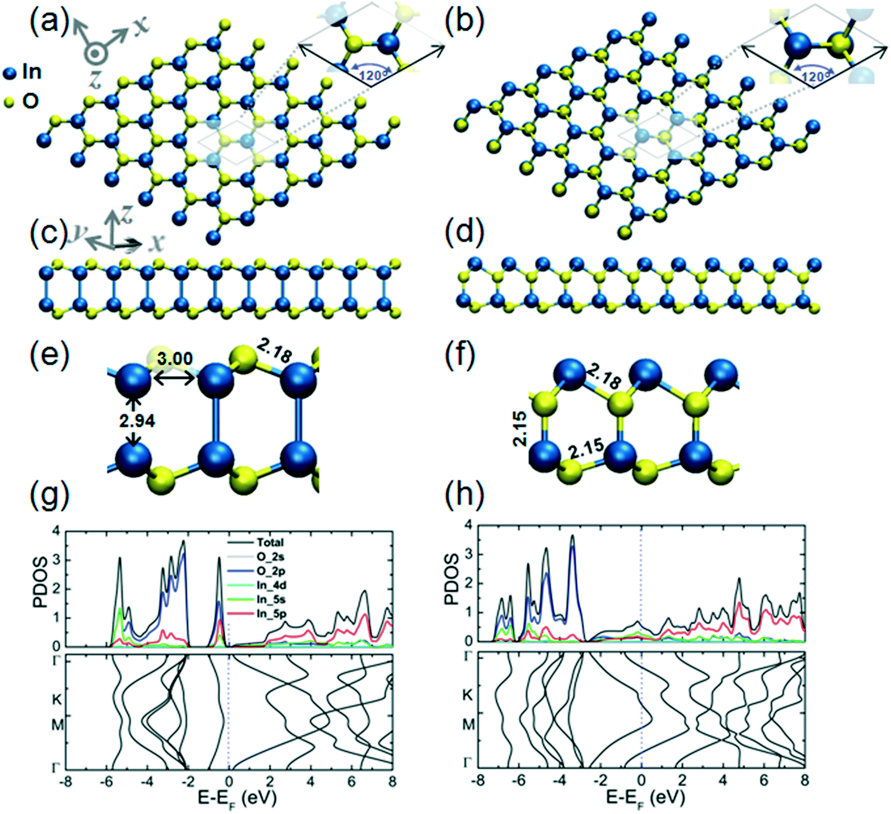 | ||
Fig. 1 Structure of a 2D InO quadruple-layer with an internal layer sequence in the form of O–In–In–O from top (a), side (c) and magnified side views (e), with characteristic atomic distances indicated. The unit cell is depicted in (a). This unit cell comprises two In atoms and two O atoms, the lengths of the ![[a with combining right harpoon above (vector)]](https://www.rsc.org/images/entities/i_char_0061_20d1.gif) and and ![[b with combining right harpoon above (vector)]](https://www.rsc.org/images/entities/i_char_0062_20d1.gif) cell vectors reading || = || = 3.51 Å, with an angle between them of 120 degrees. Plots of partial density of states (PDOS) and the band structure of the 2D InO quadruple-layer with internal layer sequence O–In–In–O are presented in panel (g). The structure of an alternative 2D InO quadruple-layer with internal layer sequence in the form of O–In–O–In in from top (b), side (d) and magnified side views (f), with characteristic atomic distances indicated. The unit cell is depicted in (b). This unit cell comprises two In atoms and two O atoms, the lengths of the and cell vectors reading || = || = 3.56 Å, with an angle between them of 120 degrees. Plots of the partial density of states (PDOS) and band structure of the 2D InO quadruple-layer with internal layer sequence O–In–O–In are presented in panel (h). cell vectors reading || = || = 3.51 Å, with an angle between them of 120 degrees. Plots of partial density of states (PDOS) and the band structure of the 2D InO quadruple-layer with internal layer sequence O–In–In–O are presented in panel (g). The structure of an alternative 2D InO quadruple-layer with internal layer sequence in the form of O–In–O–In in from top (b), side (d) and magnified side views (f), with characteristic atomic distances indicated. The unit cell is depicted in (b). This unit cell comprises two In atoms and two O atoms, the lengths of the and cell vectors reading || = || = 3.56 Å, with an angle between them of 120 degrees. Plots of the partial density of states (PDOS) and band structure of the 2D InO quadruple-layer with internal layer sequence O–In–O–In are presented in panel (h). | ||
Plots of the partial density of states (PDOS) and band structure for the two alternative 2D InO monolayers are presented in Fig. 1(g) and (h), respectively. The analysis of the components of the calculated orbital projection for the quadruple-layer of sequence O–In–In–O in Fig. 1(e) reveals that its top of the valence band (TVB) is contributed by the 2p-orbital of the oxygen atoms and by the 5p-orbital of the indium atoms, while the bottom of the conduction band (BCB) is formed by the contribution of the 2p-orbital of the oxygen atoms and by the 5s-orbital of the indium atoms. This 2D InO structure exhibits an indirect bandgap of 0.48 eV. The exact value of the calculated band gap should be taken cautiously as most DFT methods significantly underestimate the band gap of materials.29 We note that in a previous broad study dedicated to several different 2D metal oxides,8 a band gap value of 1.22 eV at the GGA–PBE level of theory, and 4.1 eV at the HSE06 level of theory has been calculated for 2D InO in an equilibrium geometry that is similarly structured to the present quadruple-layer. Although the alternative quadruple-layer of sequence O–In–O–In, Fig. 1(f), features similar orbital contributions to its TVB and BCB, this alternative 2D InO structure appears gapless and thus metallic.
We have further explored 2D structures of indium oxide of In2O3 stoichiometry. An evocative reference for it is a planar hexagonal monolayer of h-Sc2O3, h-V2O3, and h-Mn2O3,13 h-Y2O3,14 and h-Al2O3.15 Notably, the same 2D oxide atomic structure can be shared between 3d transition metal elements (Sc, V, Mn), a 4d transition metal element (Y) and a 3p main group element (Al). Indium is another p-type element and all main group elements are generally perceived to exhibit diversity in stoichiometry and structural motifs in compounds at the 2D limit.30
In the monolayer structure of hexagonal In2O3, h-In2O3, the metal atoms can be indicated as residing in the vertices of the hexagons while the O atoms reside in the metal–metal bridge sites, as shown in Fig. 2(a). The calculated cohesive energy of this monolayer structure is 5.00 eV per atom. An alternative h-In2O3 monolayer featuring 12-membered rings has also been modeled and its structural and electronic properties are presented in Fig. 2(b). This alternative h-In2O3 monolayer exhibits a higher stability by considering the calculated value of 5.21 eV per atom of its cohesive energy. During optimization, these two structures emerge as minima on the potential energy hypersurface (PES) for the stoichiometry of In2O3 and 2D dimensionality.
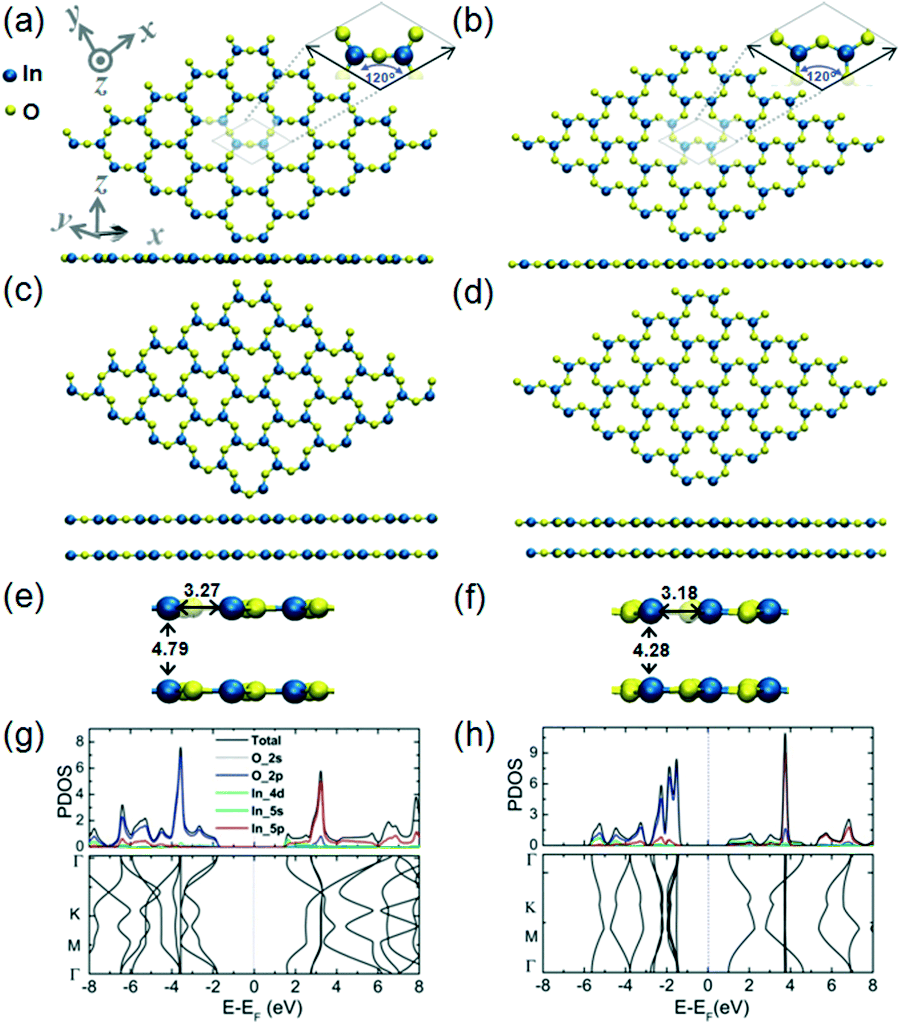 | ||
| Fig. 2 Structure of a h-In2O3 monolayer from top and side views (a), the relaxed bilayer structure from top and side views (c), and a magnified side view of the bilayer structure (e) with characteristic atomic distances indicated. The unit cell is depicted in (a). This unit cell comprises two In atoms and three O atoms, the lengths of the and cell vectors reading || = || = 5.85 Å, with an angle between them of 120 degrees. Plots of partial density of states (PDOS) and band structure are shown in (g). Structure of an alternative h-In2O3 monolayer featuring 12-membered rings from top and side views (b), the relaxed bilayer structure from top and side views (d) and a magnified side view of the bilayer structure (f) with characteristic atomic distances indicated. The unit cell is depicted in (b). This unit cell comprises two In atoms and three O atoms, the lengths of the and cell vectors reading || = || = 6.36 Å, with an angle between them of 120 degrees. Plots of partial density of states (PDOS) and band structure are shown in (h). | ||
Fig. 2(c) and (d) represent the bilayer structures associated to the corresponding h-In2O3 monolayers from Fig. 2(a) and (b) upon structural relaxation. Notably, the bilayer structure in Fig. 2(c) befits an isomeric variant to bilayer structure in Fig. 2(d) both featuring 12-membered rings.
Plots of partial density of states (PDOS) and band structure for the two alternative bilayer structures are presented in Fig. 2(g) and (h), respectively. The analysis of the components of the calculated orbital projection reveals that their top TVBs are formed essentially by the contribution of the 2p-orbital of the oxygen atoms, while their BCBs are formed by the contribution of the 5p-orbital and 5s-orbital of the indium atoms. This localization of donor and acceptor states in the band gaps may be explored to expand the utilization of these structures in low-dimensional electronic devices. The two alternative bilayer structures exhibit semiconductor behavior with direct bandgaps of 3.15 eV and 2.24 eV, respectively.
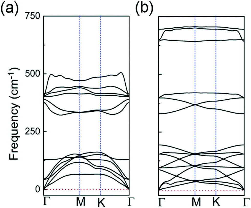 | ||
| Fig. 3 Calculated phonon spectra for: (a) the 2D InO quadruple-layer with internal layer sequence of O–In–In–O shown in Fig. 1(a); (b) the bilayer of h-In2O3 featuring 12 membered rings shown in Fig. 2(d). | ||
The studied 2D structures have been subjected to phonon spectra calculations. Among these structures, only the 2D InO quadruple-layer of sequence O–In–In–O from Fig. 1(a) and the bilayer of h-In2O3 featuring 12 membered rings from Fig. 2(d) exhibit phonon spectra without any imaginary frequencies as presented in Fig. 3(a) and (b), respectively, and therefore satisfy the phonon filter in the analysis of stability of these 2D atomic structures of indium oxide.
In an atomic resolution TEM study, both these structures would project two sub-layers of In atoms in “atop” positions with characteristic In–In distances. As indicated in Fig. 1(a), the calculated In–In distance of 2.94 Å along the z-direction, and 3.0 Å along the x-direction, respectively, matches closely with the experimental results from ref. 12. Under the deposition kinetics conditions in ref. 12, the experimental realization of 2D InO is apparently consistent with the quadruple-layer of sequence O–In–In–O as depicted in Fig. 1(a). The deposition conditions in ref. 12 are underlined by intercalation of In atoms in the confined space between SiC and graphene. The projected atomic arrangement of the intercalated In atoms appears as perfectly square with both the out-of-plane and the in-plane columnar distances reading 2.6 ± 0.1 Å.12
4. Conclusions
We give insight into an assortment of 2D structures of indium oxide of stoichiometry InO and In2O3 through first-principles calculations. Considering the increasing effort towards synthesizing 2D structures of non-van-der-Waals-type materials, these calculations can be of immediate support to experimental verifications. Noteworthily, a variety of 2D structures might be expected to be stabilized, including those perceived as metastable, and being dictated by any specifics of deposition kinetics. 2D InO has been obtained in spatial confinement between SiC and graphene,12 and the projected atomic arrangement of the intercalated In atoms has been found to be in agreement with the In–In distances predicted for the stable 2D InO structure obtained in this work. By exploring 2D structures of indium oxide of stoichiometry In2O3, we report on the structural and electronic properties of until now unexplored structures with planar hexagonal geometry.Conflicts of interest
There are no conflicts of interest to declare.Acknowledgements
RBS acknowledges support by Conselho Nacional de Desenvolvimento Científico e Tecnológico (CNPq). GKG and AKG acknowledge the support by the Swedish Research Council (VR) through VR 2017-04071. GKG further acknowledges the support by Åforsk through grant 18-266. RR acknowledges the support by Coordenação de Aperfeiçoamento de Pessoal de Nível Superior – Brasil (CAPES) – Finance Code 001 – CAPES-PrInt-UFBA, and support by CNPq. The authors acknowledge resources provided by the Swedish National Infrastructure for Computing (SNIC) at the National Supercomputer Center (NSC) in Linköping (SNIC 2020/5-146 and SNIC 2020/14-17) partially funded by the Swedish Research Council through grant agreement VR2018-05973.References
- Y. Deng, Y. Yu, M.-Z. Shi, Z. Guo, Z. Xu, J. Wang, X.-H. Chen and Y. Zhang, Quantum anomalous Hall effect in intrinsic magnetic topological insulator MnBi2Te4, Science, 2020, 367, 895 CrossRef CAS PubMed.
- E. F. de Almeida Junior, F. de Brito Mota, C. M. C. de Castilho, A. Kakanakova-Georgieva and G. K. Gueorguiev, Defects in hexagonal-AlN sheets by first-principles calculations, Eur. Phys. J. B, 2012, 85, 48 CrossRef.
- R. B. dos Santos, F. de Brito Mota, R. Rivelino, A. Kakanakova-Georgieva and G. K. Gueorguiev, Van der Waals stacks of few-layer h-AlN with graphene: An ab initio study of structural, interaction and electronic properties, Nanotechnology, 2016, 27, 145601 CrossRef PubMed.
- A. Kakanakova-Georgieva, G. K. Gueorguiev, D. G. Sangiovanni, N. Suwannaharn, I. G. Ivanov, I. Cora, B. Pécz, G. Nicotra and F. Giannazzo, Nanoscale phenomena ruling deposition and intercalation of AlN at the graphene/SiC interface, Nanoscale, 2020, 12, 19470 RSC.
- B. Pécz, G Nicotra, F. Giannazzo, R. Yakimova, A. Koos and A. Kakanakova-Georgieva, Indium Nitride at the 2D limit, Adv. Mater., 2021, 33, 2006660 CrossRef PubMed.
- H. Şahin, S. Cahangirov, M. Topsakal, E. Bekaroglu, E. Akturk, R. T. Senger and S. Ciraci, Monolayer honeycomb structures of group-IV elements and III-V binary compounds: First-principles calculations, Phys. Rev. B: Condens. Matter Mater. Phys., 2009, 80, 155453 CrossRef.
- P. Borlido, A. W. Huran, M. A. L. Marques and S. Botti, Structural prediction of stabilized atomically thin tin layers, npj 2D Mater. Appl., 2019, 3, 21 CrossRef.
- Y. Guo, L. Ma, K. Mao, M. Ju, Y. Bai, J. Zhao and X. C. Zeng, Eighteen functional monolayer metal oxides: wide band gap semiconductors with superior oxidation resistance and ultrahigh carrier mobility, Nanoscale Horiz., 2019, 4, 592 RSC.
- M. C. Lucking, W. Xie, D.-H. Choe, D. West, T.-M. Lu and S. B. Zhang, Traditional Semiconductors in the Two-Dimensional Limit, Phys. Rev. Lett., 2018, 120, 086101 CrossRef CAS PubMed.
- T. Gorkan, E. Aktürk and S. Ciraci, Deformed octagon-hexagon-square structure of group-IV and group-V elements and III-V compounds, Phys. Rev. B, 2019, 100, 125306 CrossRef CAS.
- H. Bergeron, D. Lebedev and M. C. Hersam, Polymorphism in post-dichalcogenide two-dimensional materials, Chem. Rev., 2021, 121, 2713 CrossRef CAS PubMed.
- A. Kakanakova-Georgieva, F. Giannazzo, G. Nicotra, I. Cora, G. K. Gueorguiev, P. O. Å. Persson and B. Pécz, Material proposal for 2D indium oxide, Appl. Surf. Sci., 2021, 548, 149275 CrossRef CAS.
- H. van Gog, W.-F. Li, C. Fang, R. S. Koster, M. Dijkstra and M. van Huis, Thermal stability, and electronic and magnetic properties of atomically thin 2D transition metal oxides, npj 2D Mater. Appl., 2019, 3, 18 CrossRef.
- T. T. Song, M. Yang, M. Callsen, Q. Y. Wu, J. Zhou, S. F. Wang, S. J. Wang and Y. P. Feng, Graphene stabilized high-k dielectric Y2O3 (111) monolayers and their interfacial properties, RSC Adv., 2015, 5, 83588 RSC.
- T. T. Song, M. Yang, J. W. Chai, M. Callsen, J. Zhou, T. Yang, Z. Zhang, J. S. Pan, D. X. Chi, Y. P. Feng and S. J. Wang, The stability of aluminium oxide monolayer and its interface with two-dimensional materials, Sci. Rep., 2016, 6, 29221 CrossRef CAS PubMed.
- P. Ordejón, E. Artacho and J. M. Soler, Self-consistent order-N density-functional calculations for very large systems, Phys. Rev. B: Condens. Matter Mater. Phys., 1996, 53, 10441 CrossRef PubMed.
- D. Sánchez-Portal, E. Artacho and J. M. Soler, Density-functional method for very large systems with LCAO basis sets, Int. J. Quantum Chem., 1997, 65, 453 CrossRef.
- J. Junquera, O. Paz, D. Sánchez-Portal and E. Artacho, Numerical atomic orbitals for linear-scaling calculations, Phys. Rev. B: Condens. Matter Mater. Phys., 2001, 64, 235111 CrossRef.
- N. Troullier and J. L. Martins, Efficient pseudopotentials for plane-wave calculations, Phys. Rev. B: Condens. Matter Mater. Phys., 1991, 43, 1993 CrossRef CAS PubMed.
- J. P. Perdew, K. Burke and M. Ernzerhof, Generalized Gradient Approximation Made Simple, Phys. Rev. Lett., 1996, 77, 3865 CrossRef CAS PubMed.
- R. B. dos Santos, R. Rivelino, F. de Brito Mota, G. K. Gueorguiev and A. Kakanakova-Georgieva, Dopant species with Al-Si and N-Si bonding in the MOCVD of AlN implementing trimethylaluminum, ammonia and silane, J. Phys. D: Appl. Phys., 2015, 48, 295104 CrossRef.
- R. R. Q. Freitas, F. de Brito Mota, R. Rivelino, C. M. C. de Castilho, A. Kakanakova-Georgieva and G. K. Gueorguiev, Tuning band inversion symmetry of buckled III-Bi sheets by halogenation, Nanotechnology, 2016, 27, 055704 CrossRef CAS PubMed.
- C. Goyenola, S. Stafström, L. Hultman and G. K. Gueorguiev, Structural patterns arising during synthetic growth of fullerene-like sulfocarbide, J. Phys. Chem. C, 2012, 116, 21124 CrossRef CAS.
- K. D. Bakoglidis, J. Palisaitis, R. B. dos Santos, R. Rivelino, P. O. Å. Persson, G. K. Gueorguiev and L. Hultman, Self-Healing in Carbon Nitride Evidenced As Material Inflation and Superlubric Behavior, ACS Appl. Mater. Interfaces, 2018, 10, 16238 CrossRef CAS PubMed.
- H. J. Monkhorst and J. D. Pack, Special points for Brillouin-zone integrations, Phys. Rev. B: Solid State, 1976, 13, 5188 CrossRef.
- S. Grimme, Semiempirical GGA-type density functional constructed with a long-range dispersion correction, J. Comput. Chem., 2006, 27, 1787 CrossRef CAS PubMed.
- O. I. Malyi, K. V. Sopiha and C. Persson, Energy, Phonon, and Dynamic Stability Criteria of Two-Dimensional Materials, ACS Appl. Mater. Interfaces, 2019, 11, 24876 CrossRef CAS PubMed.
- A. I. Cocemasov, V. I. Brinzariand and D. L. Nika, Energetic, structural and electronic features of Sn-, Ga-, O-based defect complexes in cubic In2O3, J. Phys.: Condens. Matter, 2020, 32, 225703 CrossRef CAS PubMed.
- K. A. Johnson and N. W. Ashcroft, Corrections to density-functional theory band gaps, Phys. Rev. B: Condens. Matter Mater. Phys., 1998, 58, 15548 CrossRef CAS.
- Z. Lu, G. P. Neupane, G. Jia, H. Zhao, D. Qi, Y. Du, Y. Lu and Z. Yin, 2D Materials Based on Main Group Element Compounds: Phases, Synthesis, Characterization, and Applications, Adv. Funct. Mater., 2020, 30, 2001127 CrossRef CAS.
| This journal is © The Royal Society of Chemistry 2021 |