DOI:
10.1039/D1CE00557J
(Paper)
CrystEngComm, 2021,
23, 5045-5052
Effects of the initial flux ratio on CeSb2 crystal growth by a self-flux method
Received
26th April 2021
, Accepted 17th June 2021
First published on 18th June 2021
Abstract
CeSb2 is a homologue of rare-earth diantimonides. This work reports a systematic study of a series of high-quality single crystals of CeSb2 grown by a self-flux method, which is a heavy fermion Kondo metal with intricate magnetic transitions. We have grown four types of crystals with different initial material ratios in order to investigate the effect of growth conditions on the quality of the as-grown crystals. The phase purity, morphology and composition of the synthesized samples were studied with X-ray diffraction, scanning electron microscopy, electron-probe microanalysis, and Raman-scattering spectroscopy to evaluate their quality. It is found that an inappropriate raw material ratio will lead to the inhomogeneity and poor crystallinity of the as-grown crystal. In addition, the electrical transport properties of the as-grown crystals were measured, from which the residual resistivity ratios were extracted to further examine the homogeneity and crystalline quality. Furthermore, the magnetoresistance properties of CeSb2 were observed. Through a systematic study on CeSb2, the most suitable starting ratio for the growth of CeSb2 was obtained, which might serve as a guide for the growth of other light rare-earth diantimonides.
1. Introduction
During the last few decades, rare-earth compounds have aroused broad interest in both fundamental and applied fields.1–5 Unlike other rare-earth compounds, studies on rare-earth antimonides are quite lacking. The past reports mainly focused on the magnetic and electrical transport properties, which largely depends on the growth of high-quality crystals.6–11 However, there is still a lack of investigation on the impact of crystal quality on the transport properties. Previous studies reported that rare-earth antimonides belong to the Ruderman–Kittel–Kasuya–Yosida (RKKY) interaction system.6 In this system, the interaction between the conduction electrons and local magnetic moment (f electrons) leads to a strong RKKY interaction, which triggers lots of novel physical phenomena at low temperatures. CeSb2 is a homologue of rare-earth diantimonides ReSb2.7 The earliest report on light rare-earth diantimonides ReSb2 (Re = rare-earth element) was in 1967, R. Wang et al. used X-ray diffraction to study the lattice structure of LaSb2, CeSb2, NdSb2, and SmSb2, and gave the atomic occupancies.8 Later, studies on rare-earth diantimonides doped with various rare-earth elements on the Re site with a similar ReSb2 structure were reported.9–12 However, unlike considerable research on other rare-earth compound systems, research on rare-earth antimonides is quite lacking and existing research mainly focuses on their magnetic and electrical transport properties, which depend on high-quality crystal growth. In the current limited reports, some intriguing physical phenomena have been found in the ReSb2 system. The superconductivity was found below ∼0.4 K in LaSb2 as reported in ref. 12. Strong anisotropic ferromagnetism and magnetoresistance (MR) effects were found in CeSb2, and its temperature and field-dependent transport behavior was considered to be similar with some heavy fermions and Kondo lattice materials, such as CeCu6.11,13,14 Several low-temperature and high-temperature phase transitions were found in PrSb2.10 The low-temperature transitions were demonstrated as magnetic ordering transitions, while the high-temperature ones originated from a certain kind of density wave.10,15 Among them, CeSb2 is the most reported one. We note that CeSb2 belongs to a heavy-fermion material with strong electron correlations and some abnormal transport properties of specific heat and resistivity, and behaves differently from an ordinary metal.16 According to the Kondo lattice model, the f electrons of the Re element are localized at high temperature, while their exchange coupling to the conduction electrons leads to the formation of bands with heavy masses as the temperature is lowered, causing the f electrons to become itinerant.17–19 Therefore, new ordered phases are always generated in heavy-fermion materials, such as superconductivity and magnetic order, which make CeSb2 a promising material for further deep research. The local magnetic moment of Ce is expected to interact with the surrounding conduction electrons, resulting in hybridization. Due to this hybridization, the effective mass of electrons near the Fermi surface is quite large, which is hundreds or thousands of times larger than the free electron mass. Central to understanding heavy-fermion systems is the interplay of localization and itinerancy.19 High-quality crystals are significant for the localization and itinerancy of the conduction electrons in rare-earth alloy system materials. Hence, in this work, we grew high-quality crystals for follow-up studies.
Early synthesis of light rare-earth diantimonides employed the high-temperature and high-pressure method. ReSb2 crystals were grown at 600–1500 °C with a pressure higher than 20 kbars. A series of compounds such as GdSb2, LaSb2, and CeSb2 were successfully synthesized. However, the size and quality of these crystals are not ideal.20 In 1991, Canfield et al. successfully grew single crystals of CeSb2 by the self-flux method.13 Since then, most single crystals of CeSb2 were grown by this method. Although the physical properties of CeSb2 have been reported, studies of optimizing crystal growth are still lacking. Through our experiments, we have found that the phase purity and quality of CeSb2 crystals have a great impact on the physical properties. Optimizing the growth conditions can help improve crystal quality, which is beneficial to the following research on exploring its abundant physics. CeSb2 crystallizes in the orthorhombic Cmca space group, with lattice constants a = 6.295 Å, b = 6.124 Å and c = 18.212 Å.8,21 According to the Ce–Sb phase diagram reported in ref. 22 and 23, CeSb2 can be grown with variable ratios of raw materials as long as the molar ratio of Sb is greater than 68%. However, crystals grown under different conditions may vary greatly in crystalline quality, phase purity, and morphology.24,25
High-quality crystals are significant for elucidating their intrinsic localization and itinerancy of conduction electrons. To date, studies of the effect of self-flux configurations on the grown CeSb2 have not been reported. In this study, we focus on the growth of single crystals of CeSb2 under different molar ratios of raw materials to investigate the optimal configurations of self-flux. A series of single crystals of CeSb2 were grown and measured to determine the effect of molar ratios of Ce and Sb on their growth. Furthermore, the electrical transport measurements reveal the complex magnetic and electrical behavior of CeSb2, which provides a better understanding of the physics in rare-earth antimonides.
2. Materials and methods
2.1. Synthesis process
Single crystals of CeSb2 were grown by the self-flux method within a graphite resistance heating system and the growth temperature was monitored by thermocouples. The schematic diagram of the crystal growth apparatus is shown in Fig. 1(a). High purity Ce grains (Aladdin, 99.99%) and Sb grains (Aladdin, 99.99%) were used as raw materials, among which, Sb acts as self-flux. Hence we emphasize that the concentration of Sb is significant for growth. According to the Ce–Sb phase diagram, the flexible solvent and solidified crystal in the crucible should be separated rapidly when the melting zone temperature is just higher than 900 K to avoid the Sb element wrapping the crystal and ensure its integrity.
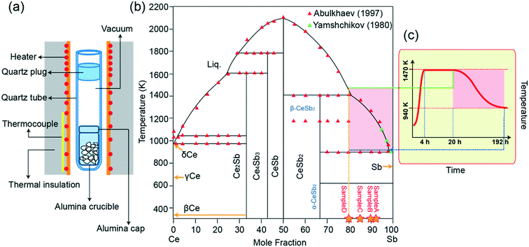 |
| | Fig. 1 (a) Sample assembly for synthesis of CeSb2 by a self-flux method. (b) Ce–Sb phase diagram and (c) temperature–time profile of the growth process. | |
Four samples were grown with different molar ratios of raw materials, in which the molar ratios of Ce are 8%, 10%, 15%, and 20%. The other growth parameters of the four samples are exactly the same. For convenience, samples grown with 8%, 10%, 15%, and 20% molar ratios of Ce are named as sample A, sample B, sample C, and sample D, respectively. Ce and Sb grains with the above four atomic ratios were fully mixed in alumina crucibles, and then the crucibles were covered with an alumina cap to prevent the raw materials from overflowing. After that the crucibles were sealed under vacuum in four quartz tubes, where sealing is achieved by melting the quartz plug and the quartz tube together through a hydrogen–oxygen flame. The mixtures were heated to 1470 K for 4 h and kept at this temperature for 16 h to make the molten Ce and Sb mix evenly, and then slowly cooled down to 940 K for 168 h. After that, the crystal and solvent are separated by high-speed centrifugation at 940 K and a block of the as-grown CeSb2 sample was obtained. These as-grown samples are naturally cleaved, showing flat and shiny facets, as shown in Fig. 2.
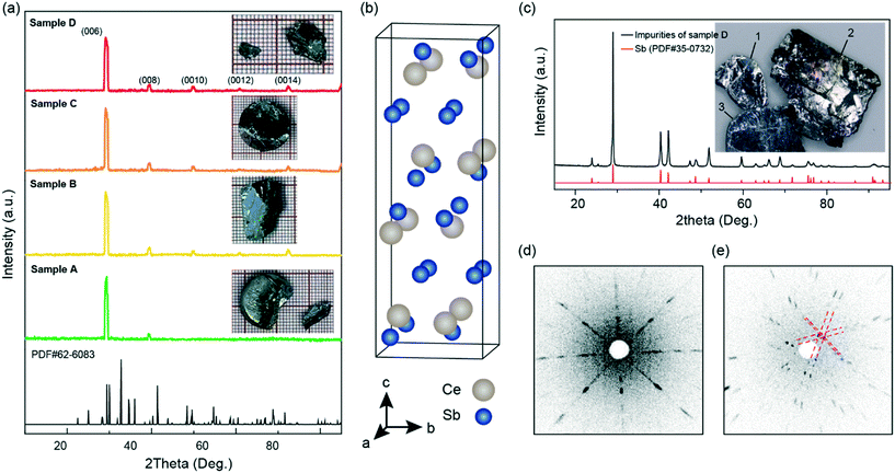 |
| | Fig. 2 Structural characterization of the as-grown CeSb2 single crystals. (a) Single crystal XRD patterns of the cleaved as-grown crystals, (b) side view of the crystal structure of CeSb2, (c) XRD measurement of the impurities in sample D. The inset of (c) shows the three pieces cleaved from one ingot. Pieces of No. 1 and 2 are mainly CeSb2 single crystals, while No. 3 is mainly Sb single crystals with the hexagonal C63/mmc space group. (d) Laue patterns of (d) CeSb2 (sample A) and (e) Sb (sample D) single crystals. | |
2.2. Characterization
X-ray diffraction (XRD) was performed with a BRUKER/AXS D8 Advance X-ray diffractometer using Cu Kα1 radiation from 10° to 90° with a step of 0.02°. Laue measurements were performed with the Multiwire Laboratories MWL120 back reflection Laue crystal orientation system. Micro Raman-scattering measurements were performed at room temperature with a Horiba confocal Raman microscope LabRAM XploRA, which was excited with a 532 nm laser. The electron-probe microanalysis (EPMA) was used to detect the chemical compositions of the as-grown sample on a Shimadzu EPMA-1720 system with energy-dispersive X-ray (EDX) spectroscopy function at an accelerating voltage of 15 kV, a probe current of 10.0 mA, and a probe electron beam diameter of 5 μm. The morphology of the samples was observed using a Hitachi S-3400N scanning electron microscope (SEM). The transport properties were measured using a Quantum Design physical property measurement system (PPMS).
3. Results and discussion
3.1. Structural characterization
The optical images and single crystal XRD patterns of the cleaved surface of the as-grown crystals are shown in Fig. 2(a). Single crystals of CeSb2 obtained with the four molar ratios of Ce can be cleaved naturally, presenting a flat cleavage surface. It is shown that the cleaved samples A, B and C have relatively large crystalline size, while sample D is more fragmented. Based on the calculated powder X-ray diffraction patterns of CeSb2, the diffraction peaks of the cleaved surfaces are found in the standard ab-plane. This proves that the as-grown samples have a single-crystal structure without polycrystalline inclusions or misoriented blocks, indicating that no second phase emerged during the rapid cooling process of centrifugation. Moreover, we note that sample D was covered by a large number of impurities. The impurities were analyzed by powder XRD measurements, and the results are shown in Fig. 2(c). By comparing with the standard pattern, it can be determined that the impurities covering the surface of sample D were Sb flux. Considering the same growth conditions of these four samples, only sample D was found to be covered by a large amount of Sb. We speculate that the amount of Sb flux is too small, which decreased the solubility of Ce and inhibited the synthesis of CeSb2. Therefore, a lot of raw Sb materials remained on the surface of sample D after crystal growth, which resulted in the poor size and integrity of sample D. In addition, the difference in the thermal expansion coefficient between impurities and the crystal can cause non-ignorable thermal stress inside the crystal during the cooling process, which may lead to the cracking of the crystal. Fig. 2(d) and (e) show the X-ray Laue diffraction of sample A and Sb impurities peeled off from sample D, respectively. The bright scattering spots in Fig. 2(d) demonstrates that the cleaved sample is of reasonably high quality. This also manifests the fourfold symmetry of the crystal structure, corresponding to its orthorhombic structure. Besides, the Sb impurities present three-dimensional symmetry in Fig. 2(e), which indicates that Sb crystallizes in the hexagonal C63/mmc space group. The dashed sublines in Fig. 2(e) indicate the twin crystal structure of Sb crystallization.
3.2. EPMA and EDX analysis
Next, we carried out EPMA and EDX measurements on the as-cleaved samples to check if there exist CeO2 or any other impurities. EDX is used for qualitative testing of elements, while EPMA is used for quantitative analysis. The EPMA results are presented in Table 1. Six different positions of the samples evenly distributed on the surface have been chosen to determine the molar ratio of Ce and Sb atoms. Finally we obtained the actual composition of Ce and Sb by calculating the average value of the six positions. Since Sb originates from the solvent of Ce–Sb mixture, although the solvent and crystals are separated by the exact centrifugation process, some Sb remains inevitably on the surface of the crystal, which caused the nominal ratio in some positions of the samples from the EDX spectroscopy. It also shows that except for sample A, all the other three samples contain a certain amount of oxygen. Since cerium is easily oxidized to CeO2 in air, the residual Ce which didn't take part in the reaction would lead to the presence of oxygen in some samples. The EDX results indicate that for sample A, Ce almost completely reacted in the growth process, since the O element was not found in the results. Furthermore, we note that the molar ratio of Sb in sample D is the largest among all the samples. However, the initial molar ratio of Sb in sample D is the lowest among all the samples. This result is consistent with our speculation that the deficiency of flux leads to the suppression of the growing CeSb2. To be specific, the decrease of the Sb concentration led to a sharp reduction of Ce solubility, which directly affected the absolute reaction of Ce and Sb, and thus increased the impurity content in the as-grown sample D. In the synthesis reaction of the CeSb2 crystal, Ce and Sb react in a molar ratio of 1![[thin space (1/6-em)]](https://www.rsc.org/images/entities/char_2009.gif) :2. Therefore, incomplete reaction will produce more residual Sb, which leads to the molar ratio of Sb in sample D being the largest among all the samples. Therefore, our experiments suggest that the molar ratio of Ce in the raw material should be ∼8% in order to assure that the raw materials would react thoroughly and obtain crystals with a lower content of impurities.
:2. Therefore, incomplete reaction will produce more residual Sb, which leads to the molar ratio of Sb in sample D being the largest among all the samples. Therefore, our experiments suggest that the molar ratio of Ce in the raw material should be ∼8% in order to assure that the raw materials would react thoroughly and obtain crystals with a lower content of impurities.
Table 1 Element contents of the as-grown samples determined by EPMA
| Sample |
Ce (Mol%) |
Sb (Mol%) |
O (Mol%) |
Ce:Sb |
| A |
32.717 |
67.283 |
0 |
1:2.06 |
| B |
33.676 |
64.881 |
1.443 |
1:1.93 |
| C |
33.732 |
64.662 |
1.606 |
1:1.92 |
| D |
30.206 |
68.692 |
1.102 |
1:2.27 |
3.3. Morphological characterization
Fig. 3 shows the SEM images of the four samples. Compared with other samples, sample A and sample B show a relatively flat surface, which reflects the high quality of these two samples. It also shows that some impurities stick on the samples, among which sample D has a large number of impurities under the microscope. According to the above analysis, the impurities in sample A are mainly Sb particles, while in samples B–D are mainly CeO2. As the impurity particles adhere to the crystal surface, the difference in the thermal expansion coefficient between the impurities and crystals can cause thermal stress inside the crystals during the cooling process. We consider that the oxidation of Ce introduces non-negligible stress in the matrix phase (both Ce and CeO2 have a cubic structure with the space group Fm![[3 with combining macron]](https://www.rsc.org/images/entities/char_0033_0304.gif) m, and the lattice parameters of Ce are a = b = c = 5.14 Å, while a = b = c = 5.51 Å for CeO2), the unreacted Ce impacted more seriously on the crystal surfaces compared with the influence of residual unreacted Sb. By SEM measurements, the surface morphology of samples A–D and the fractured cleavage of sample D also proved the above speculation. Besides, the SEM results present that CeSb2 possesses a typical layered structure.
m, and the lattice parameters of Ce are a = b = c = 5.14 Å, while a = b = c = 5.51 Å for CeO2), the unreacted Ce impacted more seriously on the crystal surfaces compared with the influence of residual unreacted Sb. By SEM measurements, the surface morphology of samples A–D and the fractured cleavage of sample D also proved the above speculation. Besides, the SEM results present that CeSb2 possesses a typical layered structure.
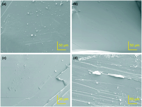 |
| | Fig. 3 SEM images of the surface of (a) sample A, (b) sample B, (c) sample C and (d) sample D. | |
3.4. Raman scattering
The Raman-scattering spectra of samples A–D are shown in Fig. 4. We choose four positions of each sample uniformly distributed on the surface to measure the Raman spectra. The Raman results of each measured positions are highly consistent, which suggests the uniformity of the as-grown samples. Fig. 4(a) shows the measured original Raman spectra for samples A–D which were collected under the same experimental conditions exactly. We immediately note that samples A and B have stronger intensity than samples C and D, which reflects the better crystal quality to some extent. Fig. 4(b) and (c) present the spectra which are normalized at a wavenumber of 200 cm−1 which belongs to the background area of the spectra. As shown in Fig. 4(a)–(c), the Raman spectra of CeSb2 crystals show three peaks at wavenumbers around 112 cm−1, 149 cm−1, and 275 cm−1. When it comes to the exact same experimental conditions for samples A–D, the full width at half maximum (FWHM) of the Raman peak reflects the impurities and defect density of the material.26,27Fig. 4(d–i) show the fitting results of peaks 1–3. Fig. 4(c), (e) and (g) show the peak positions of peaks 1–3, respectively. Fig. 4(d), (f) and (h) show the FWHM and error bars of each fitting Raman peak, respectively. It should be noted that the FWHM and the fitting error bars of peak 3 are larger than those of peaks 1 and 2. This situation may affect the reliability of these fitting data to some extent. By comparing the fitting results of the experimental data under the same conditions, we concluded that sample A possesses the highest quality among all samples.
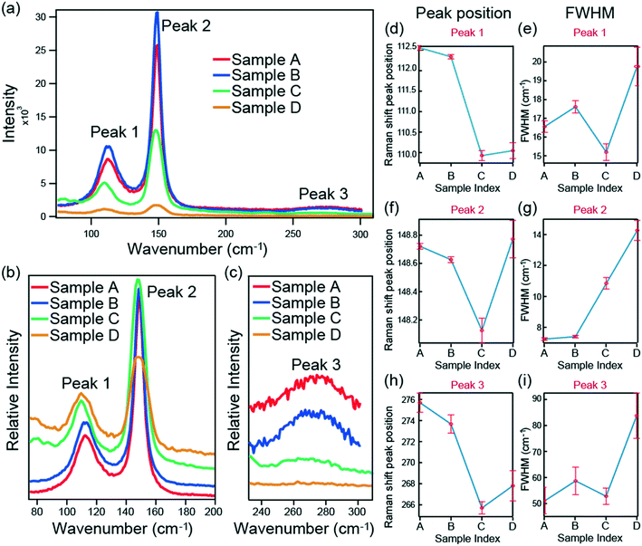 |
| | Fig. 4 Raman-scattering results of the as-grown samples. (a) Original data for Raman spectra. (b) and (c) are the normalized spectra. (d–i) are the peak positions and FWHM of peaks 1–3 obtained by a Lorentzian fit. | |
3.5. Transport measurement
In order to further characterize the quality of the as-grown samples, we carried out the electrical transport measurements. The results of the zero-field resistivity versus temperature ρ(T) are presented in Fig. 5. It is shown that with the decrease of resistivity, two broad peaks appear at ∼100 K and ∼25 K, which is quite similar to other typical Kondo lattice systems.28–30 According to previous studies, the peak at ∼100 K is normally attributed to crystal-field splitting, while the peak at ∼25 K is due to the formation of a coherent state.28–30 The value of residual resistivity ratio (RRR) reflects the purity and integrity of the alloy since the scattering of impurities and defects on electrons has a significant effect on the residual resistivity. The RRR of samples A–D was calculated by the formula RRR = ρ(300 K)/ρ(2 K), where ρ(300 K) and ρ(2 K) are the resistivity of the material at 300 K and 2 K, respectively. The RRR results of the as-grown samples are shown in Fig. 5(b). It shows that sample A has the highest RRR value and lowest room temperature resistivity, (higher than the results in ref. 6 and 11), which indicates the best quality of sample A. Overall, the crystal quality evaluated from resistivity measurements is consistent with the other results mentioned before.
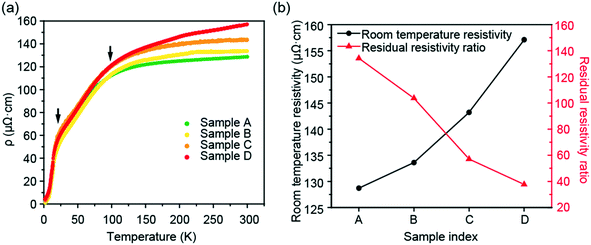 |
| | Fig. 5 (a) Temperature dependent zero-field resistivity of the as-grown samples. (b) Room temperature resistivity and the RRR value of the as-grown samples. | |
3.6. Magnetoresistance properties
In Fig. 6, we show the field-dependent resistivity of sample A. We also calculated the value of MR at various temperatures. Here, the MR is the variation of a material's resistance in response to an applied magnetic field, which can be calculated by the formula 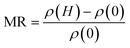 , with ρ(0) is the zero-field resistivity and ρ(H) is the resistivity under an applied magnetic field H.31,32 The MR results of CeSb2 are shown in Fig. 6. The MR data at different temperatures were measured with the field which is normal to the ab-plane. It is shown that there are at least two abnormal transitions induced by the external magnetic field at low temperature in the MR curves, which is consistent with previous reports on the magnetic transitions of CeSb2 at low temperatures.7,33,34 The transitions induced by the field disappear when the temperature becomes higher than 10 K, while the anomalous MR effect induced by magnetic transitions disappears at ∼50 K. Moreover, the MR value reaches the maximum value at 3 K, which is higher than 100%. This also shows that CeSb2 exhibits a positive MR value at a low temperature region but negative at high temperature. The negative MR can be understood in the context of the Kondo effect.35–37 In this scenario, the Kondo singlet state can be partially broken by the magnetic field, which releases the localized d-band electrons and thus lowers the resistivity. In contrast, the positive MR might be induced by the orbital-scattering effect.38 The intricate MR effect suggests that CeSb2 can be a promising candidate material in magnetic sensors, magnetic memory, or other spintronic devices. Further detailed research is required in order to clarify the cause of this abnormal MR.
 |
| | Fig. 6 Field-dependent MR of CeSb2 at different temperatures: (a) 3–12 K and (b) 14–77 K. | |
4. Conclusion
In this work, we reported the self-flux growth of single crystals of CeSb2 with different raw material configurations. We obtained large size crystals from all the four groups, and three of them possess high crystalline quality with a layered structure. The crystals can be naturally cleaved along the ab-plane cleavage surface. The quality of the as-grown crystals was characterized by XRD, Laue diffraction, SEM, Raman-scattering spectroscopy, EDX, and EPMA. The results show that the sample grown with 8% Ce ratio has the highest crystal quality. Besides, when the proportion of Ce in the raw materials is higher than 10%, a large amount of Ce will cluster on the surface of the crystal and be oxidized to CeO2, which will cause cracks inside the crystal and reduce the quality of the as-grown crystals. The electrical transport properties of the as-grown crystals were investigated by PPMS. We found that CeSb2 grown at 8% Ce ratio has the highest RRR value and the lowest room temperature resistivity, which supports the best quality of the crystal. We conclude that a Ce ratio of 8% is the suitable growth ratio for the self-flux method growth of high-quality CeSb2 crystals. On the other hand, at this ratio, the raw materials can be completely melted at a temperature lower than 1170 K, which avoids the generation of β-CeSb2. These results serve as a guide to synthesize single crystals of other light rare-earth diantimonides. In addition, the unusual magnetoresistance properties suggested that CeSb2 is a promising quantum material in spintronic applications. Our work lays the foundation for the crystal growth of CeSb2 and related compounds, and other studies.
Author contributions
S. L. Zhang and Y. F. Fang synthesized and characterized the samples. Y. F. Fang suggested the idea and supervised the experiments. Prof. Y. Hang administrated this project and provided key suggestions on the crystal growth. Y. L. Yang, C. C. Zhao and M. Z. He have taken part in the discussion on the experimental results and writing. The manuscript was mainly written by S. L. Zhang and Y. F. Fang, and revised by M. T. Li.
Conflicts of interest
There are no conflicts to declare.
Acknowledgements
We gratefully acknowledge Prof. Guangai Sun, Dr. Benqiong Liu at China Academy of Engineering Physics for their fruitful discussions. We also appreciate Prof. Zhiqiang Zou, Dr. Qi Yao and Mr. Lun Li at ShanghaiTech University, Prof. Fei Chen at Shanghai University, and Mr. Boyi Bin at Shanghai Institute of Optics and Fine Mechanics for their help with the transport measurements. This work is mainly sponsored by Shanghai Sailing Program No. 20YF1455100. Mingtao Li is financially supported by the Natural Science Foundation of China (No. 11804011).
References
- S. Jin, T. H. Tiefel, M. McCormack, R. A. Fastnacht, R. Ramesh and L. Chen, Thousandfold change in resistivity in magnetoresistive La-Ca-Mn-O films, Science, 1994, 264, 413–415 CrossRef CAS PubMed.
- K. Kadir, T. Sakai and I. Uehara, Synthesis and structure determination of a new series of hydrogen storage alloys; RMg2Ni9 (R= La, Ce, Pr, Nd, Sm and Gd) built from MgNi2 Laves-type layers alternating with AB5 layers, J. Alloys Compd., 1997, 257, 115–121 CrossRef CAS.
- R. Nikolaev, V. Sulyaeva, A. Alekseev, A. Sukhikh, E. Polyakova, T. Pomelova, T. Kuzuya, S. Hirai and B. Tran Nhu, Growth mechanism of helical γ-Dy2S3 single crystals, CrystEngComm, 2021, 23, 2196–2201 RSC.
- A. V. Kimel, A. Kirilyuk, A. Tsvetkov, R. V. Pisarev and T. Rasing, Laser-induced ultrafast spin reorientation in the antiferromagnet TmFeO3, Nature, 2004, 429, 850–853 CrossRef CAS PubMed.
- S. Huang, Y. Zhuang, Y. Zhu, Y. Yin, Y. Wan, D. Zhou, X. Chaud, L. Zhou and X. Yao, Tuning oxygen vacancy and growth step for the high performance of Nd1+xBa2−xCu3Oy bulk cryomagnets, CrystEngComm, 2020, 22, 5375–5381 RSC.
- Y. Zhang, X. Zhu, B. Hu, S. Tan, D. Xie, W. Feng, Q. Liu, W. Zhang, Y. Liu, H. Song, L. Luo, Z. Zhang and X. Lai, Anisotropic and mutable magnetization in Kondo lattice CeSb2, Chin. Phys. B, 2017, 26, 067102 CrossRef.
- M. A. Ruderman and C. Kittel, Indirect Exchange Coupling of Nuclear Magnetic Moments by Conduction Electrons, Phys. Rev., 1954, 96, 99 CrossRef CAS.
- R. Wang and H. Steinfink, The crystal chemistry of selected AB2 rare earth compounds with selenium, tellurium, and antimony, Inorg. Chem., 1967, 6, 1685–1692 CrossRef CAS.
- N. Sato, T. Kinokiri, T. Komatsubara and H. Harima, Effect of quasi-two-dimensional Fermi surfaces on electronic properties in YbSb2, Phys. Rev. B: Condens. Matter Mater. Phys., 1999, 59, 4714 CrossRef CAS.
- K. Kawaguchi, T. Kagayama, G. Oomi, P. C. Canfield and S. L. Bud'ko, Electrical resistance of PrSb2 under high pressure, Phys. Rev. B: Condens. Matter Mater. Phys., 1997, 237, 587–589 CrossRef.
- S. L. Bud'ko, Anisotropic magnetic properties of light rare-earth diantimonides, Phys. Rev. B: Condens. Matter Mater. Phys., 1998, 57, 13624 CrossRef.
- F. Hullinger and H. R. Ott, Superconductivity of lanthanum pnictides, J. Less-Common Met., 1977, 55, 103–113 CrossRef.
- P. C. Canfield, J. D. Thompson and Z. Fisk, Novel Ce magnetism in CeDipnictide and Di-Ce pnictide structures, J. Appl. Phys., 1991, 70, 5992–5994 CrossRef CAS.
- P. T. Coleridge, Magnetoresistance and growth of the coherent state in CeCu6, J. Phys. F: Met. Phys., 1987, 17, 79 CrossRef.
- N. Kawakami and A. Okiji, Magnetoresistance of the Heavy-Electron Ce Compounds, J. Phys. Soc. Jpn., 1986, 55, 2114 CrossRef CAS.
- G. Oomi, T. Kagayama, K. Kawaguchi, P. C. Canfield and S. L. Bud'ko, Effect of pressure and magnetic field on the electrical resistance of PrSb2, Phys. Rev. B: Condens. Matter Mater. Phys., 1997, 230, 776–779 CrossRef.
- C. M. Varma, Mixed-valence compounds, Rev. Mod. Phys., 1976, 48, 219 CrossRef CAS.
- G. R. Stewart, Heavy-fermion systems, Rev. Mod. Phys., 1984, 56, 755 CrossRef CAS.
- Q. Chen, D. Xu, X. Niu, J. Jiang, R. Peng, H. Xu, C. Wen, Z. Ding, K. Huang, L. Shu, Y. Zhang, H. Lee, V. Strocov, M. Shi, F. Bisti, T. Schmitt, Y. Huang, P. Dudin, X. Lai, S. Kirchner, H. Yuan and D. Feng, Direct observation of how the heavy-fermion state develops in CeCoIn5, Phys. Rev. B, 2017, 96, 045107 CrossRef.
- N. L. Eatough and H. T. Hall, High-pressure synthesis of rare earth diantimonides, Inorg. Chem., 1969, 8, 1439–1445 CrossRef CAS.
- A. Borsese, G. Borzone, D. Mazzone and R. Ferro, Heats of formation of Ce-Sb alloys, J. Less-Common Met., 1981, 79, 57–63 CrossRef CAS.
- V. D. Abulkhaev, Phase diagram of the Ce-Sb system, Zhurnal Neorganicheskoj Khimii, 1997, 42, 341–345 CAS.
- X. Su and J. C. Tedenac, Thermodynamic modeling of the ternary Ce–Fe–Sb system: Assessment of the Ce–Sb and Ce–Fe systems, Calphad, 2006, 30, 455–460 CrossRef CAS.
- G. Ray, N. Sinha, S. Bhandari, B. Singh, I. Bdikin and B. Kumar, Flux growth of 0.94 [Na0.5K0.5NbO3]–0.06 LiNbO3 piezo−/ferroelectric crystals for long duration and high temperature applications, CrystEngComm, 2014, 16, 7004–7012 RSC.
- C. Guguschev, D. Klimm, F. Langhans, Z. Galazka, D. Kok, U. Juda and R. Uecker, Top-seeded solution growth of SrTiO3 crystals and phase diagram studies in the SrO–TiO2 system, CrystEngComm, 2014, 16, 1735–1740 RSC.
- K. Sinha, A. Mascarenhas, G. Horner, K. Bertness, S. Kurtz and J. Olson, Raman line-shape analysis of random and spontaneously ordered GaInP2 alloy, Phys. Rev. B: Condens. Matter Mater. Phys., 1994, 50, 7509 CrossRef CAS PubMed.
- H. Lin, R. Chen, Y. Huo, T. Kamins and J. Harris, Raman study of strained Ge1− xSnx alloys, Appl. Phys. Lett., 2011, 98, 261917 CrossRef.
- B. Cornut and B. Coqblin, Influence of the crystalline field on the Kondo effect of alloys and compounds with cerium impurities, Phys. Rev. B: Solid State, 1972, 5, 4541 CrossRef.
- J. Ray, E. V. Sampathkumaran and G. Chandra, Resistance anomalies in the Kondo-lattice system CeCu2− xNixSi2, Phys. Rev. B: Condens. Matter Mater. Phys., 1987, 35, 2095 CrossRef CAS PubMed.
- J. S. Schilling, Possible origin of the resistivity maximum in heavy-fermion systems, Phys. Rev. B: Condens. Matter Mater. Phys., 1986, 33, 1667 CrossRef CAS PubMed.
-
A. B. Pippard, Magnetoresistance in Metals, Cambridge University, Cambridge, England, 1989 Search PubMed.
- S. A. Wolf, D. D. Awschalom, R. A. Buhrman, J. M. Daughton, S. von Molnár, M. L. Roukes, A. Y. Chtchelkanova and D. M. Treger, Spintronics: a spin-based electronics vision for the future, Science, 2001, 294, 1488–1495 CrossRef CAS PubMed.
- T. Pérez-Castañeda, J. Azpeitia, J. Hanko, A. Fente, H. Suderow and M. A. Ramos, Low-Temperature Specific Heat of Graphite and CeSb2: Validation of a Quasi-adiabatic Continuous Method, J. Low Temp. Phys., 2013, 173, 4–20 CrossRef.
- B. Liu, L. Wang, I. Radelytskyi, Y. Zhang, M. Meven, H. Deng, F. Zhu, Y. Su, X. Zhu, S. Tan and A. Schneidewind, Neutron scattering study of commensurate magnetic ordering in single crystal CeSb2, J. Phys.: Condens. Matter, 2020, 32, 405605 CrossRef CAS PubMed.
- A. N. Pasupathy, R. C. Bialczak, J. Martinek, J. E. Grose, L. A. K. Donev, P. L. McEuen and D. C. Ralph, The Kondo effect in the presence of ferromagnetism, Science, 2004, 306, 86–89 CrossRef CAS PubMed.
- H. Xue, Y. Hong, C. Li, J. Meng, Y. Li, K. Liu, M. Liu, W. Jiang, Z. Zhang, L. He, R. Dou, C. Xiong and J. Nie, Large negative magnetoresistance driven by enhanced weak localization and Kondo effect at the interface of LaAlO3 and Fe-doped SrTiO3, Phys. Rev. B, 2018, 98, 085305 CrossRef CAS.
- J. Jiang, S. Li, T. Zhang, Z. Sun, F. Chen, Z. Ye, M. Xu, Q. Ge, S. Tan, X. Niu, M. Xia, B. Xie, Y. Li, X. Chen, H. Wen and D. Feng, Observation of possible topological in-gap surface states in the Kondo insulator SmB6 by photoemission, Nat. Commun., 2013, 4, 1–8 CAS.
- F. J. Wong, R. V. Chopdekar and Y. Suzuki, Disorder and localization at the LaAlO3/SrTiO3 heterointerface, Phys. Rev. B: Condens. Matter Mater. Phys., 2010, 82, 165413 CrossRef.
|
| This journal is © The Royal Society of Chemistry 2021 |
Click here to see how this site uses Cookies. View our privacy policy here. 
 ab,
Mingtao
Li
c,
Yilun
Yang
ab,
Chengchun
Zhao
ab,
Mingtao
Li
c,
Yilun
Yang
ab,
Chengchun
Zhao


 , with ρ(0) is the zero-field resistivity and ρ(H) is the resistivity under an applied magnetic field H.31,32 The MR results of CeSb2 are shown in Fig. 6. The MR data at different temperatures were measured with the field which is normal to the ab-plane. It is shown that there are at least two abnormal transitions induced by the external magnetic field at low temperature in the MR curves, which is consistent with previous reports on the magnetic transitions of CeSb2 at low temperatures.7,33,34 The transitions induced by the field disappear when the temperature becomes higher than 10 K, while the anomalous MR effect induced by magnetic transitions disappears at ∼50 K. Moreover, the MR value reaches the maximum value at 3 K, which is higher than 100%. This also shows that CeSb2 exhibits a positive MR value at a low temperature region but negative at high temperature. The negative MR can be understood in the context of the Kondo effect.35–37 In this scenario, the Kondo singlet state can be partially broken by the magnetic field, which releases the localized d-band electrons and thus lowers the resistivity. In contrast, the positive MR might be induced by the orbital-scattering effect.38 The intricate MR effect suggests that CeSb2 can be a promising candidate material in magnetic sensors, magnetic memory, or other spintronic devices. Further detailed research is required in order to clarify the cause of this abnormal MR.
