
Effects of growth substrate on the nucleation of monolayer MoTe2†
David J.
Hynek
a,
Raivat M.
Singhania
b,
James L.
Hart
a,
Benjamin
Davis
b,
Mengjing
Wang
a,
Nicholas C.
Strandwitz
b and
Judy J.
Cha
 *a
*a
aEnergy Sciences Institute, Department of Mechanical Engineering and Materials Science, Yale University, West Haven, CT 06516, USA. E-mail: judy.cha@yale.edu
bDepartment of Materials Science and Engineering, Lehigh University, Bethlehem, PA 18015, USA
First published on 29th March 2021
Abstract
The discovery and characterization of two-dimensional (2D) materials beyond graphene has increased dramatically over the past decade with increasingly fine control over the growth dynamics of these materials. MoTe2 represents a model material for studying phase change properties of 2D materials due to small energy differences between its 2H semiconducting phase and 1T′ semimetallic phase. Although some substrates are demonstrated to be better than others for the wafer-scale growth of high quality MoTe2 films, substrate effects on the nucleation and growth of MoTe2 are still not well understood. Here, we grow monolayer MoTe2 by converting MoOx thin films deposited on three different substrates: sapphire Al2O3 (0001), amorphous SiO2, and amorphous AlOx, and examine the early stages of the conversion reaction to elucidate the substrate effects on the nucleation of MoTe2. We observe that the chemical composition of the substrate is more important than the surface topography and crystallinity of the substrate, with high quality monolayer 2H MoTe2 formed on both Al2O3 (0001) and AlOx in contrast to mixed phase 2H/1T′ MoTe2 formed on SiO2, as determined by Raman spectroscopy, X-ray photoelectron spectroscopy, and atomic force microscopy.
Introduction
Due to their low-dimensionality and layer-dependent properties, 2D materials have been heavily studied in recent years for their potential applications that range from catalysis1 to energy storage.2 Transition metal dichalcogenides (TMDCs) of the form MX2 (M: Mo, W; X: S, Se, Te) represent a particularly heavily studied subset of 2D materials due to the wide variety of electronic phases readily accessible, expanding their uses in next-generation electronics. Of these TMDCs, MoTe2 has gained recent attention for potential applications in phase-change memory and low power electronics due to small free energy differences between its semiconducting 2H (α) phase and semimetallic 1T′ (β) phase at room temperature,3 and between semimetallic 1T′ (β) phase and topological Td (γ) phase at low temperatures.4,5 Many studies have shown useful physical characteristics including superconductivity,6–8 a possible quantum spin Hall state,9 and reversible phase switching,10–12 yet, reliable large-scale growth of MoTe2 with thickness control and high crystallinity has remained a challenge.Several physical and electrical characterization studies have been carried out using MoTe2 flakes obtained by exfoliation or chemical vapor deposition (CVD),8,13,14 but these methods suffer from low yield and a lack of scalability. We have recently demonstrated synthesis of thickness-controlled MoTe2 films through the tellurization of MoOx (2 < x < 3) thin films deposited by atomic layer deposition (ALD), where the number of ALD cycles determined the thickness of the MoTe2 films.15 The MoTe2 films were uniform across a wafer scale and could be synthesized on Al2O3 (0001) down to a monolayer. In this work, we examined the effects of substrate composition and structure on the nucleation and crystallinity of MoTe2 thin films when MoTe2 was converted from ALD-deposited MoOx thin films. To determine how the growth of MoTe2 is affected by the chemical composition or crystallinity of the underlying substrate, we utilized the following substrates: sapphire Al2O3 (0001), 3 nm-thick ALD-deposited amorphous AlOx on SiO2/Si, and amorphous SiO2. We show that the complete conversion from MoOx to monolayer 2H MoTe2 can be achieved on both Al2O3 (0001) and amorphous AlOx while only mixed phase 2H/1T′ films were realized on amorphous SiO2. Our results indicate that chemical composition plays a more important role than the crystallinity or surface topography of the growth substrate.
Results and discussion
Amorphous MoOx films were deposited by ALD on sapphire Al2O3 (0001), 3 nm-thick ALD-deposited amorphous AlOx, and amorphous SiO2 (Methods). Based on our previous study,15 MoOx thin films of 8 and 10 ALD cycles were chosen to grow monolayer MoTe2 in order to maximize the effects of the substrate on the crystalline quality of MoTe2 while a MoOx film of 120 ALD cycles was used to grow a thick MoTe2 for transmission electron microscopy (TEM) characterization. The oxide films were tellurized in a two-zone furnace under an H2/Ar atmosphere at 600 °C for three different time intervals: 15 minutes, 20 minutes, and 50 minutes (Fig. 1e, see Methods for synthesis details). This 8–10 cycle synthesis resulted in a discontinuous, polycrystalline film (Fig. S1a and b†), where the individual domains consisted of monolayer 2H MoTe2, with an average domain size of 10–20 nm. The discontinuity observed in MoTe2 is due to the fact that 8 and 10 ALD cycle MoOx films were not sufficiently thick to form a continuous monolayer. Uniform and continuous 2H MoTe2 films were obtained using the 120 ALD cycle MoOx films deposited on amorphous AlOx (Fig. 1f and g). The selected area electron diffraction and high-resolution TEM images confirm the 2H phase for MoTe2. | ||
| Fig. 1 Growth of 2H MoTe2 converted from MoOx thin films. a and b) 2H MoTe2 viewed along b- and c-axis. c and d) 1T′ MoTe2 viewed along b- and c-axis. e) Two-zone furnace growth schematic. f) TEM image taken along the c-axis, showing a 2H MoTe2 film, converted from 120 ALD cycle-thick MoOx grown on 3 nm-thick amorphous AlOx. Scale bar, 100 nm. (Inset) selected area electron diffraction from (f). Scale bar, 10 nm−1. g) High resolution TEM image of the film shown in (f). Scale bar, 3 nm. | ||
The evolution of the crystalline phase of the MoTe2 films on the three different substrates was tracked throughout the length of the 50 minute reaction after three different time intervals (15 minutes, 20 minutes, and 50 minutes) using Raman spectroscopy (Fig. 2) (Methods). The 2H phase is characterized by two main modes at 170 cm−1 (A1g) and 234 cm−1 (E2g1),16–18 while the 1T′ phase is characterized by a primary mode at 163 cm−1 (Ag4).19 For MoTe2 synthesis, it is known that the 1T′ phase is initially synthesized due to the Te- deficient stoichiometry and a 2H phase can nucleate out of the 1T′ phase with the continual supply of Te vapor3,15 (Fig. S2†). After a 15 minute growth, only the 8 cycle-thick MoOx film on amorphous AlOx has converted fully to 2H MoTe2, while the MoTe2 on Al2O3 (0001) and amorphous SiO2 shows a mixed phase of 2H and 1T′. After 20 minutes of growth, MoTe2 on the Al2O3 (0001) substrate has also fully converted to 2H, while the MoTe2 on amorphous SiO2 still remains mixed-phase. From 20 to 50 minutes of growth, the growth result did not change substantially, with MoTe2 on the AlOx and Al2O3 (0001) substrates remaining in the 2H phase, and MoTe2 on the SiO2 not converting fully to the 2H phase (Fig. 2d). We observe the same trend when 10 cycle-thick MoOx films were converted to MoTe2 on the three substrates (Fig. S3†).
 | ||
| Fig. 2 Raman spectroscopy characterization of MoTe2 films converted on different substrates at varying reaction times. Raman spectra of MoTe2 converted from 8 cycle-thick MoOx deposited on Al2O3 (0001) (a), amorphous SiO2 (b), and amorphous AlOx (c). Spectra were captured after three different intervals for each sample: 15 minutes (black), 20 minutes (red), and 50 minutes (blue). Overlaid spectra from all three substrates after 50 minutes of growth are shown in (d). | ||
The progression of the MoTe2 films from MoOx is further characterized using X-ray photoelectron spectroscopy (XPS) (Fig. 3). Mo has two primary peaks at 228 eV (3d5/2) and 231 eV (3d3/2),20 with Mo-oxide peaks at slightly higher binding energies. By tracking the intensity of the oxide peaks as a function of reaction time, the reaction time needed to transform MoOx to MoTe2 was determined for each substrate. In agreement with the Raman results, after 15 minutes of reaction, MoTe2 converted on the amorphous AlOx substrate is shown to have the least amount of oxidized Mo. MoTe2 converted on Al2O3 (0001) and amorphous SiO2 substrates still show significant amounts of Mo-oxide peaks, suggesting incomplete conversion to MoTe2. After 20 minutes of reaction, all films show almost a complete reduction in Mo-oxide peaks, with little change from 20 to 50 minutes of reaction. Interestingly, a residual amount of MoOx remains in the MoTe2 films converted on the amorphous SiO2 and amorphous AlOx substrates, with a higher concentration evident in the SiO2 substrate, and no residual oxidation is observed in the MoTe2 converted on sapphire (Fig. 3d). This residual MoOx may be from surface oxidation of MoTe2, or due to non van der Waals bonding at the interface between MoTe2 and the two amorphous substrates. If the residual MoOx were from the surface oxidation of MoTe2, the MoOx peaks should be present for MoTe2 on all three substrates, which is not the case. Thus, the residual MoOx observed for the two amorphous substrates cannot be attributed to the surface oxidation of MoTe2. This hypothesis is further supported by very little oxidation in the Te peaks for all three substrates after 50 minutes of reaction (Fig. S4†). The absence of the oxide peaks for MoTe2 converted on Al2O3 (0001) thus suggests that the residual MoOx is either from the chemical bonds of MoTe2 to the amorphous oxide substrates or from the diffusion of Mo atoms into the amorphous oxide substrates. We note the residual MoOx is not reflected in the O 1s binding energy, which is dominated by the oxygen of the underlying substrates (Fig. S5†). The same result is observed when 10 cycle-thick MoOx films were converted on the three substrates (Fig. S6†).
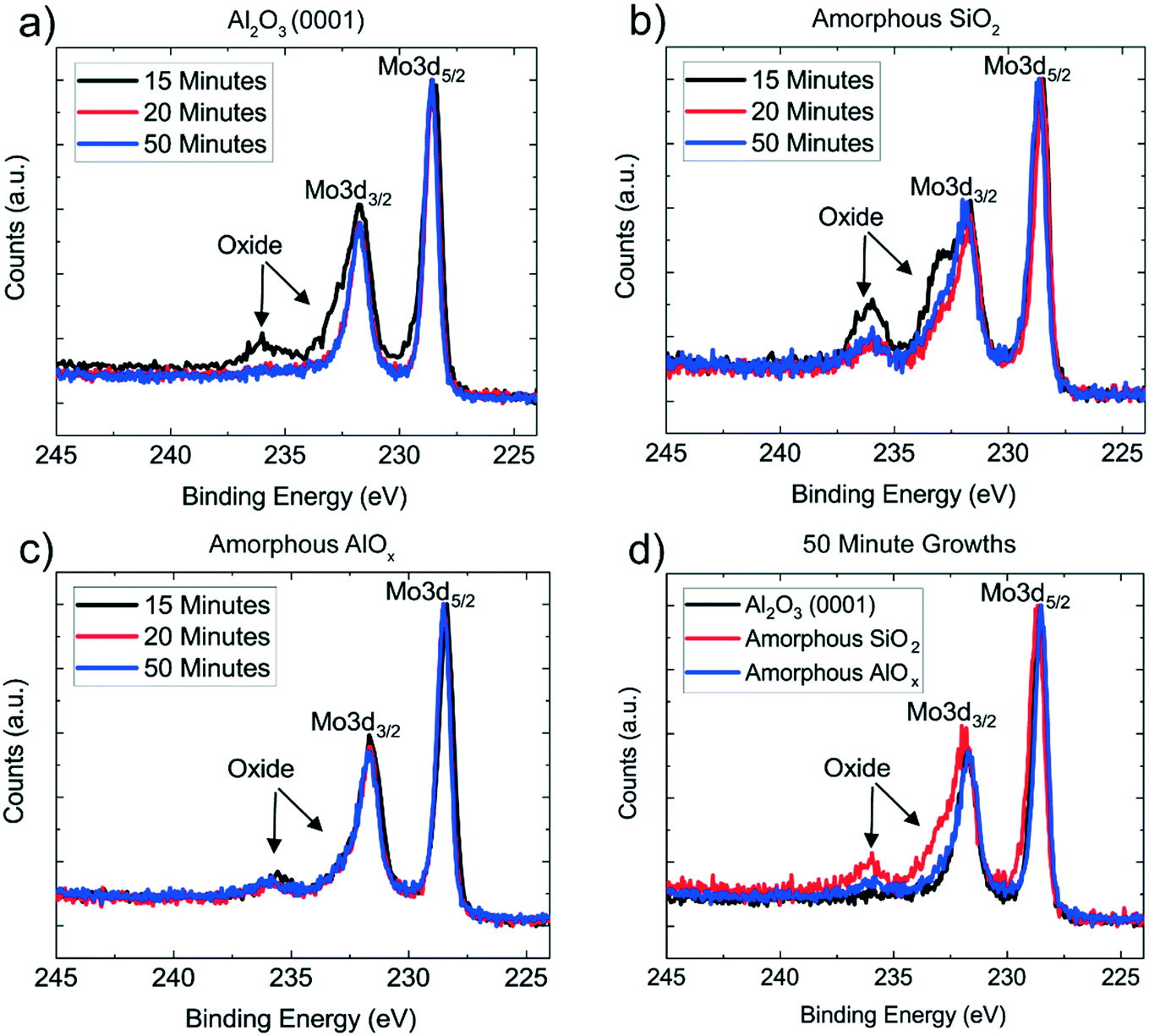 | ||
| Fig. 3 XPS analysis of Mo 3d peaks in MoTe2 films converted on different substrates at varying reaction times. XPS of Mo 3d peaks in MoTe2 films converted from 8 cycle-thick MoOx deposited on Al2O3 (0001) (a), amorphous SiO2 (b), and amorphous AlOx (c). Spectra were captured after three different intervals for each sample: 15 minutes (black), 20 minutes (red), and 50 minutes (blue). Overlaid spectra from all three substrates after 50 minutes of growth are shown in (d). | ||
We also investigated the topography of the MoTe2 films using atomic force microscopy (AFM). Fig. 4 shows the changes in topography of MoTe2 as a function of substrate and reaction time. Before the reaction, the surface roughness of the MoOx films deposited on the three substrates was measured, showing that the Al2O3 (0001) case is the most flat and films grown on amorphous AlOx and SiOx substrates have higher surface roughness similar to each other. No significant changes were observed in the surface roughness after annealing the MoOx films in H2/Ar environment at 600 °C (Fig. S7†). After the conversion to MoTe2, the height distribution profiles show that the surface roughness of MoTe2 on all three substrates is much larger than the initial surface roughness of the substrates (Fig. 4e, j and o), indicating the formation of discontinuous monolayer MoTe2 islands of domain size in the 10's of nm range (Fig. 4d, i and n). This is due to the insufficient number of ALD cycles for the initial MoOx precursor film for the synthesis of continuous monolayer MoTe2 and could be remedied by increasing the thickness of the MoOx film.15 MoTe2 films converted on Al2O3 (0001) are the most flat, while MoTe2 films converted on amorphous AlOx became slightly rougher as the conversion continued from 15 minutes to 50 minutes of reaction time. In contrast, the surface roughness of the MoTe2 on the SiO2 substrate did not appear to change after the initial 15 minutes of reaction and, after 50 minutes of reaction, the surface roughness of the MoTe2 is the largest on SiO2. The same trend in surface roughness was observed for MoTe2 films converted from 10 cycle-thick MoOx films (Fig. S8†).
 | ||
| Fig. 4 AFM characterization of MoTe2 films converted on different substrates at varying reaction times. AFM images of MoTe2 converted from 8 cycle-thick MoOx deposited on Al2O3 (0001) (a–d), amorphous SiO2 (f–i), and amorphous AlOx (k–n) after different reaction times. Scale bars, 100 nm. Height profiles for the three substrates (e, j and o) were obtained by averaging the height distributions of four AFM images taken from each sample, 8 μm distance from one another at each time point: 0 minutes (cyan, pristine oxide), 15 minutes (black), 20 minutes (red), and 50 minutes (blue). | ||
The Raman and XPS analysis suggest that MoTe2 conversion occurs most quickly on the amorphous AlOx substrate and most slowly on the amorphous SiO2 substrate. Additionally, residual MoOx peaks remain for MoTe2 converted on amorphous substrates, possibly suggesting chemical bonding at the interface between MoTe2 and the substrate. Therefore, from the combination of Raman spectroscopy, XPS, and AFM analysis, we conclude that the chemistry of the substrate has a major role in the nucleation of 2H monolayer MoTe2 films from precursor MoOx films. One reason this could occur is the overall diffusivity of the MoOx films on SiO2vs. AlOx. It has been shown previously that MoOx shows greater diffusivity on amorphous AlOx than it does on amorphous SiO2,21 indicating stronger wetting between MoOx and AlOx. Growth of other TMDCs on AlOx and SiOx substrates has also been examined. When WS2 was synthesized directly on different substrates by ALD using WF6 and H2S as precursors, the Delabie group at University of Leuben showed that WS2 on amorphous AlOx and sapphire Al2O3 grew in a layer-by-layer manner,22 while WS2 on amorphous SiO2 grew in a 3D manner as clusters.23 Their results suggest that the W precursor interacts more strongly with sapphire Al2O3 or AlOx than with SiO2, similar to the diffusivity case of MoOx on AlOxvs. SiO2. Additionally, it has been shown that adhesion of metal atoms to oxide supports depends more strongly on the choice of oxide support rather than the metal.24 Thus, these studies provide strong evidence that the conformal synthesis of 2D materials on AlOxvs. SiOx substrates is driven by better adhesion between metal atoms (Mo or W) and the oxide substrates underneath, as opposed to crystallinity of the substrates. We also note that strain imparted from the substrate due to different degrees of thermal expansion could stabilize the 1T′ phase over the 2H phase. It has been shown that CVD grown WSe2 on SiO2 experience significant tensile strain due to a large mismatch between the thermal expansion coefficient values, while WSe2 grown on sapphire experience little strain due to similar thermal expansion coefficients.25 This could be significant as the phase transition of MoTe2 is sensitive to strain.26 In addition to the effect of substrate composition on the nucleation and film uniformity of MoTe2, we further observe that substrate crystallinity affects the bonding at the interface between MoTe2 and substrate: MoOx is present at the interface between MoTe2 and amorphous AlOx while it is absent between MoTe2 and crystalline Al2O3. Although a relationship has been determined for MoTe2 on the three different substrates, conclusive physical explanations for why adhesion energies of metal atoms on different oxide substrates are different are unclear.24
Conclusion
While large-area synthesis of MoTe2 thin films has been demonstrated previously, the impact of chemistry and crystallinity of the substrate on the nucleation and crystalline quality of MoTe2 has been unclear. Here, we show that the conversion of MoOx to monolayer 2H MoTe2 proceeds at comparable rates on amorphous AlOx and Al2O3 (0001), while the conversion is slower on SiO2. We conclude that this is due to increased wetting between Te or Mo atoms on the surface of AlOx compared to SiOx, allowing for improved lateral mobility and reconfiguration to successfully realize the 2H phase. This work shows the need for further studies regarding substrate interactions during synthesis of 2D materials and for increased understanding of the diffusion of metal species on oxide films.Methods
Atomic layer deposition of MoOx films and substrate preparation
Silicon wet thermal oxide substrates (500 nm, University Wafer) were prepared using a standard RCA process. Samples were immersed in a 5![[thin space (1/6-em)]](https://www.rsc.org/images/entities/char_2009.gif) :1:1 volume ratio solution of deionized (18 MΩ) H2O (18.2 MΩ):NH4OH:H2O2 and subsequently immersed in a 6:1:1 solution of DI H2O:HCl:H2O2. Both rinses were conducted for 10 min between 70 and 80 °C and were immediately followed by a DI H2O rinse.
:1:1 volume ratio solution of deionized (18 MΩ) H2O (18.2 MΩ):NH4OH:H2O2 and subsequently immersed in a 6:1:1 solution of DI H2O:HCl:H2O2. Both rinses were conducted for 10 min between 70 and 80 °C and were immediately followed by a DI H2O rinse.
Atomic layer deposition of 3 nm thick AlOx films was performed in a Cambridge Nanotech S-100 reactor at a substrate temperature of 200 °C. The silicon thermal oxide substrates (500 nm, University Wafer) were first pretreated with UV-ozone for 2 minutes. Trimethylaluminum (TMA) and O3 were utilized as precursors for 30 cycles of ALD, giving approximately 3 nm of amorphous AlOx on the surface of the thermal oxide substrate.
Sapphire substrates were cleaned in a modified version of the RCA process.27 The first step was a soak in an ethanol bath for 12 hours at room temperature, followed by a rinse with DI H2O. Samples were then sonicated for 30 min at room temperature in a 1:20:79 solution of detergent:ethanol:DI H2O. Samples were then soaked in a 3:1 H2SO4:H2O2 piranha solution. Finally, samples were immersed in more concentrated variants of the standard RCA solutions, comprising 2:1:1 DI H2O:NH4OH:H2O2 and 2:1:1 DI H2O:HCl:H2O2. Each of the latter 3 rinses was conducted for 20 min at 80 °C and was followed with a DI H2O rinse. All samples were dried with high purity nitrogen gas between each step.
Atomic layer deposition of MoOx films was performed in a Cambridge Nanotech S-100 reactor at a substrate temperature of 200 °C. Bis(tert-butylimido)bis(dimethylamido)molybdenum (NtBu)2(NMe2)2Mo and ozone were utilized as precursors in accordance with a previously published procedure.28 Films of different thicknesses were synthesized using cycle numbers of 8, 10, and 120.
Conversion of MoOx to MoTe2 films
MoTe2 thin films were synthesized through the annealing of MoOx thin films of various thicknesses grown by ALD in a tellurium atmosphere. Te powder (2 g, Sigma-Aldrich, 99.999%) was placed in a 2 inch quartz tube at zone 1 of a two-zone furnace (MTI OTF-1200X-II), while MoOx thin films on various substrates were placed downstream in the second zone of the tube furnace. After purging the tube many times with Ar to ensure no residual oxygen was present, the two zones were heated to 570 °C for Te powder and 600 °C for MoOx films in 15 min and held there for 50 minutes total, with characterization conducted after 3 different time intervals: 15 minutes, 20 minutes, and 50 minutes. A mixture of H2/Ar was flowed at 100/10 sccm in atmospheric pressure during the reaction. After the synthesis was completed, the chamber was purged with 200 sccm Ar gas for 25 minutes, and then rapidly cooled to room temperature by opening the furnace cover. We note that the samples were removed from the furnace for characterization between the three time intervals. Thus, the samples were first reacted for 15 minutes, then for additional 5 minutes (denoted as ‘20 minutes’), and finally for additional 30 minutes (denoted as ‘50 minutes’).Structural and chemical characterization
Plan-view TEM images were taken at 200 kV using a Tecnai Osiris microscope at the Yale Institute for Quantum Engineering (YINQE). All plan-view MoTe2 films were grown on amorphous AlOx substrates for easy lift-off using hydrofluoric acid as etching of sapphire for lift-off was proven difficult and the lifted MoTe2 films were transferred onto carbon covered Quantifoil TEM grids with equally spaced 2 μm holes. To characterize the surface of the films, atomic force microscopy was conducted using a Cypher ES microscope from Asylum Research. The microscope was operated in peak-force tapping mode. Raman spectroscopy (Horiba) was used to verify film uniformity and characterize the thickness and phase of the MoTe2 films. The laser used was 633 nm, with a laser power of 10% and diffraction grating 1800 g mm−1. Full conversion of the films from MoOx to MoTe2 was verified through X-ray photoelectron spectroscopy (XPS) (PHI VersaProbe II).Conflicts of interest
There are no conflicts to declare.Acknowledgements
D. J. H. was supported by the NASA graduate student fellowship #80NSSC19K1131. J. J. C. acknowledges support from DOE BES DE-SC0014476. N. C. S and B. D. acknowledge support from the National Science Foundation Grant No. 1605129. The following user facilities are acknowledged for instrument use, scientific and technical assistance: the Yale West Campus Materials Characterization Core (MCC), the Yale West Campus Imaging Core, and the Yale Institute for Nanoscience and Quantum Engineering (YINQE).References
- D. Deng, K. S. Novoselov, Q. Fu, N. Zheng, Z. Tian and X. Bao, Catalysis with Two-Dimensional Materials and Their Heterostructures, Nat. Nanotechnol., 2016, 11, 218–230 Search PubMed.
- B. Xu, S. Qi, M. Jin, X. Cai, L. Lai, Z. Sun, X. Han, Z. Lin, H. Shao, P. Peng, Z. Xiang, J. E. ten Elshof, R. Tan, C. Liu, Z. Zhang, X. Duan and J. Ma, 2020 Roadmap on Two-Dimensional Materials for Energy Storage and Conversion, Chin. Chem. Lett., 2019, 30, 2053–2064 Search PubMed.
- X. Xu, S. Chen, S. Liu, X. Cheng, W. Xu, P. Li, Y. Wan, S. Yang, W. Gong, K. Yuan, P. Gao, Y. Ye and L. Dai, Millimeter-Scale Single-Crystalline Semiconducting MoTe2 via Solid-to-Solid Phase Transformation, J. Am. Chem. Soc., 2019, 141, 2128–2134 Search PubMed.
- Y. Tao, J. A. Schneeloch, C. Duan, M. Matsuda, S. E. Dissanayake, A. A. Aczel, J. A. Fernandez-Baca, F. Ye and D. Louca, Appearance of a Td* Phase across the Td-T′ Phase Boundary in the Weyl Semimetal MoTe2, Phys. Rev. B, 2019, 100, 100101(R) Search PubMed.
- C. Heikes, I. L. Liu, T. Metz, C. Eckberg, P. Neves, Y. Wu, L. Hung, P. Piccoli, H. Cao, J. Leao, J. Paglione, T. Yildirim, N. P. Butch and W. Ratcliff, Mechanical Control of Crystal Symmetry and Superconductivity in Weyl Semimetal MoTe2, Phys. Rev. Mater., 2018, 2, 074202 Search PubMed.
- Y. Qi, P. G. Naumov, M. N. Ali, C. R. Rajamathi, W. Schnelle, O. Barkalov, M. Hanfland, S.-C. Wu, C. Shekhar, Y. Sun, V. Sü, M. Schmidt, U. Schwarz, E. Pippel, P. Werner, R. Hillebrand, T. Förster, E. Kampert, S. Parkin, R. J. Cava, C. Felser, B. Yan and S. A. Medvedev, Superconductivity in Weyl Semimetal Candidate MoTe2, Nat. Commun., 2016, 7, 11038 Search PubMed.
- S. Cho, S. H. Kang, H. S. Yu, H. W. Kim, W. Ko, S. W. Hwang, W. H. Han, D. Choe, Y. H. Jung, K. J. Chang, Y. H. Lee, H. Yang and S. W. Kim, Te Vacancy-Driven Superconductivity in Orthorhombic Molybdenum Ditelluride, 2D Mater., 2017, 4, 021030 Search PubMed.
- W. Wang, S. Kim, M. Liu, F. A. Cevallos, R. J. Cava and N. P. Ong, Evidence for an Edge Supercurrent in the Weyl Superconductor MoTe2, Science, 2020, 368, 534–537 Search PubMed.
- X. Qian, J. Liu, L. Fu and J. Li, Quantum Spin Hall Effect in Two-Dimensional Transition Metal Dichalcogenides, Science, 2014, 346, 1344–1347 Search PubMed.
- W. Hou, A. Azizimanesh, A. Sewaket, T. Peña, C. Watson, M. Liu, H. Askari and S. M. Wu, Strain-Based Room-Temperature Non-Volatile MoTe2 Ferroelectric Phase Change Transistor, Nat. Nanotechnol., 2019, 14, 668–673 Search PubMed.
- Y. Wang, J. Xiao, H. Zhu, Y. Li, Y. Alsaid, K. Y. Fong, Y. Zhou, S. Wang, W. Shi, Y. Wang, A. Zettl, E. J. Reed and X. Zhang, Structural Phase Transition in Monolayer MoTe2 Driven by Electrostatic Doping, Nature, 2017, 550, 487–491 Search PubMed.
- C. Zhang, S. KC, Y. Nie, C. Liang, W. G. Vandenberghe, R. C. Longo, Y. Zheng, F. Kong, S. Hong, R. M. Wallace and K. Cho, Charge Mediated Reversible Metal−Insulator Transition in Monolayer MoTe2 and WxMo1−xTe2 Alloy, ACS Nano, 2016, 10, 7370–7375 Search PubMed.
- M. J. Mleczko, A. C. Yu, C. M. Smyth, V. Chen, Y. C. Shin, S. Chatterjee, Y. C. Tsai, Y. Nishi, R. M. Wallace and E. Pop, Contact Engineering High-Performance n-Type MoTe2 Transistors, Nano Lett., 2019, 19, 6352–6362 Search PubMed.
- N. R. Pradhan, D. Rhodes, S. Feng, Y. Xin, S. Memaran, B. H. Moon, H. Terrones, M. Terrones and L. Balicas, Field-Effect Transistors Based on Few-Layered α-MoTe2, ACS Nano, 2014, 8, 5911–5920 Search PubMed.
- D. J. Hynek, R. M. Singhania, S. Xu, B. Davis, L. Wang, M. Yarali, J. V. Pondick, J. M. Woods, N. C. Strandwitz and J. J. Cha, Cm2-Scale Synthesis of MoTe2 Thin Films with Large Grains and Layer Control, ACS Nano, 2021, 15, 410–418 Search PubMed.
- C. Ruppert, O. B. Aslan and T. F. Heinz, Optical Properties and Band Gap of Single- and Few-Layer MoTe2 Crystals, Nano Lett., 2014, 14, 6231–6236 Search PubMed.
- M. Grzeszczyk, K. Gołasa, M. Zinkiewicz, K. Nogajewski, M. R. Molas, M. Potemski, A. Wysmołek and A. Babiñski, Raman Scattering of Few-Layers MoTe2, 2D Mater., 2016, 3, 025010 Search PubMed.
- Q. J. Song, Q. H. Tan, X. Zhang, J. B. Wu, B. W. Sheng, Y. Wan, X. Q. Wang, L. Dai and P. H. Tan, Physical Origin of Davydov Splitting and Resonant Raman Spectroscopy of Davydov Components in Multilayer MoTe2, Phys. Rev. B, 2016, 93, 115409 Search PubMed.
- J. Wang, X. Luo, S. Li, I. Verzhbitskiy, W. Zhao, S. Wang, S. Y. Quek and G. Eda, Determination of Crystal Axes in Semimetallic T′-MoTe2 by Polarized Raman Spectroscopy, Adv. Funct. Mater., 2017, 27, 1604799 Search PubMed.
- J.-H. Huang, H.-H. Hsu, D. Wang, W.-T. Lin, C.-C. Cheng, Y.-J. Lee and T.-H. Hou, Polymorphism Control of Layered MoTe2 through Two-Dimensional Solid-Phase Crystallization, Sci. Rep., 2019, 9, 8810 Search PubMed.
- W. Xu, J. Yan, N. Wu, H. Zhang, Y. Xie, Y. Tang, Y. Zhu and W. Yao, Diffusing Behavior of MoO3 on Al2O3 and SiO2 Thin Films, Surf. Sci., 2000, 470, 121–130 Search PubMed.
- B. Groven, A. N. Mehta, H. Bender, Q. Smets, J. Meersschaut, A. Franquet, T. Conard, T. Nuytten, P. Verdonck, W. Vandervorst, M. Heyns, I. Radu, M. Caymax and A. Delabie, Nucleation Mechanism during WS2 Plasma Enhanced Atomic Layer Deposition on Amorphous Al2O3 and Sapphire Substrates, J. Vac. Sci. Technol., A, 2018, 36, 01A105 Search PubMed.
- B. Groven, A. Nalin Mehta, H. Bender, J. Meersschaut, T. Nuytten, P. Verdonck, T. Conard, Q. Smets, T. Schram, B. Schoenaers, A. Stesmans, V. Afanas'Ev, W. Vandervorst, M. Heyns, M. Caymax, I. Radu and A. Delabie, Two-Dimensional Crystal Grain Size Tuning in WS2 Atomic Layer Deposition: An Insight in the Nucleation Mechanism, Chem. Mater., 2018, 30, 7648–7663 Search PubMed.
- S. L. Hemmingson and C. T. Campbell, Trends in Adhesion Energies of Metal Nanoparticles on Oxide Surfaces: Understanding Support Effects in Catalysis and Nanotechnology, ACS Nano, 2017, 11, 1196–1203 Search PubMed.
- G. H. Ahn, M. Amani, H. Rasool, D. H. Lien, J. P. Mastandrea, J. W. Ager, M. Dubey, D. C. Chrzan, A. M. Minor and A. Javey, Strain-Engineered Growth of Two-Dimensional Materials, Nat. Commun., 2017, 8, 608 Search PubMed.
- S. Song, D. H. Keum, S. Cho, D. Perello, Y. Kim and Y. H. Lee, Room Temperature Semiconductor−Metal Transition of MoTe2 Thin Films Engineered by Strain, Nano Lett., 2016, 16, 188–193 Search PubMed.
- D. Zhang, Y. Wang and Y. Gan, Characterization of Critically Cleaned Sapphire Single-Crystal Substrates by Atomic Force Microscopy, XPS and Contact Angle Measurements, Appl. Surf. Sci., 2013, 274, 405–417 Search PubMed.
- A. Bertuch, G. Sundaram, M. Saly, D. Moser and R. Kanjolia, Atomic Layer Deposition of Molybdenum Oxide Using Bis(Tert-Butylimido)Bis(Dimethylamido) Molybdenum, J. Vac. Sci. Technol., A, 2014, 32, 01A119 Search PubMed.
Footnote |
| † Electronic supplementary information (ESI) available. See DOI: 10.1039/d1ce00275a |
| This journal is © The Royal Society of Chemistry 2021 |