
 Open Access Article
 This Open Access Article is licensed under a Creative Commons Attribution-Non Commercial 3.0 Unported Licence
Highly-crystalline 6 inch free-standing GaN observed using X-ray diffraction topography
Jaemyung
Kim
ab,
Okkyun
Seo
abc,
L. S. R.
Kumara
abc,
Toshihide
Nabatame
a,
Yasuo
Koide
a and
Osami
Sakata
 *abcd
*abcd
aCenter for GaN Characterization and Analysis, Research Network and Facility Services Division (RNFS), National Institute for Materials Science (NIMS), Tsukuba, Ibaraki 305-0047, Japan. E-mail: SAKATA.Osami@nims.go.jp
bSynchrotron X-ray Station at SPring-8, RNFS, NIMS, Kouto, Sayo, Hyogo 679-5148, Japan
cSynchrotron X-ray Group, Research Center for Advanced Measurement and Characterization, NIMS, Kouto, Sayo, Hyogo 679-5148, Japan
dCenter for Synchrotron Radiation Research Institute (JASRI), Kouto, Sayo, Hyogo 679-5198, Japan
First published on 1st February 2021
Abstract
We demonstrate the crystal quality of a 6 inch (0001) plane free-standing GaN substrate grown using a Na-flux based liquid phase epitaxy method. The 11![[2 with combining macron]](https://www.rsc.org/images/entities/char_0032_0304.gif) 4 rocking curve profiles of every point over the substrate were recorded by synchrotron X-ray diffraction topography. The reconstructed images show that there is a huge boundary between the high crystalline area and the low crystalline area in the substrate. Anisotropic bowing of the lattice planes with respect to the [10
4 rocking curve profiles of every point over the substrate were recorded by synchrotron X-ray diffraction topography. The reconstructed images show that there is a huge boundary between the high crystalline area and the low crystalline area in the substrate. Anisotropic bowing of the lattice planes with respect to the [10![[1 with combining macron]](https://www.rsc.org/images/entities/char_0031_0304.gif) 0] direction was obtained from wafer bending analysis. The mean width of the rocking curves over the wafer was 0.024°, which indicates that the newly fabricated 6 inch GaN substrate was almost a single crystal. We found that there was a competition between crystallinity and homogeneity.
0] direction was obtained from wafer bending analysis. The mean width of the rocking curves over the wafer was 0.024°, which indicates that the newly fabricated 6 inch GaN substrate was almost a single crystal. We found that there was a competition between crystallinity and homogeneity.
Introduction
The growth of large scale GaN is important for the mass production of optoelectronic devices1,2 and power devices.3,4 In commercially available LEDs (light-emitting diodes) or GaN HEMT (high-electron mobility transistors), GaN films are grown on foreign materials such as SiC (ref. 5 and 6) and sapphire.7,8 However, because of the significant lattice mismatch between GaN and its growth substrates, threading dislocation occurs and deteriorates device performance and lifetime.9,10 Although buffer layers such as InGaN can be used between the substrate and GaN,11–14 lattice mismatch still occurs, and dislocation densities are still high.Despite significant progress in crystal growth techniques, dislocations are easily observed in GaN-based devices. In the case of a GaN laser diode, Mg-related point defects diffuse to the active layer through threading dislocation that degrades the lifetime of the device.9 It has been observed that a high dislocation density lowers drain current and the transconductance peak value and degrades the frequency response in GaN HEMT power devices.10 Accordingly, lowering the dislocation density is essential to increase device reliability and performance.
A drastic lowering of the dislocation density can be achieved by employing a GaN bulk instead of a thin film. A thick GaN boule is grown on top of a foreign substrate such as SiC,15 sapphire,16–18 and GaAs (ref. 19) with GaN seeds or various patterns. In the case of the seed-based method, the GaN seeds undergo ELO (epitaxial lateral overgrowth), forming a thick single-crystalline GaN boule.20 Free-standing GaN crystals have been obtained by separating the GaN boule from the foreign sacrificial layer using a laser lift-off process.21 However, because of the difficulty in controlling the growth rate while preserving morphological stability, it is still challenging to increase the substrate size.22 For the growth of the bulk GaN substrate, HVPE (hydride vapor phase epitaxy),23,24 ammonothermal methods,25 Li-flux based methods,26,27 and Na-flux based methods28–34 have been widely used. Among the methods, the Na-flux based LPE (liquid phase epitaxy) method has attracted attention due to its low growth temperature.
There have been many trials to increase GaN substrate size since 1996, when the first free-standing GaN crystals were obtained (around 5 mm in size).22 After one year, the crystal size had increased to 10 mm by growing crystals for 200 hours,22 and by 1998, the crystal size had increased up to 15 mm.22 The technology became commercially viable after the development of 2 inch free-standing GaN. Since that time, the wafer size increased up to 6 inch in 2018;24 however, the wafer was not characterized.
According to a recent report on 4 inch free-standing GaN grown using an HVPE method,35 the mean crystallinity over the substrate was high, showing narrow X-ray rocking curves over the substrate. The radius of curvature reached 35 m, and the mean FWHM of the GaN 114 was 33 arcsecs, which shows an almost single-crystal behaviour. However, the crystallinity of the substrate tended to decrease from the centre to the edge, including lattice plane bowing. Moreover, there was inhomogeneity in the FWHM distribution over the substrate during crystal growth, which may be related to a high dislocation density originating from the GaN seeds. The crystallinity near the GaN seed was lower than that in other places, which resulted in inhomogeneity.
Here, we present the synchrotron X-ray diffraction characterization results of 6 inch free-standing GaN grown using a Na-flux based LPE method for the first time. We discuss the crystallinity and local lattice plane shape of the whole wafer using X-ray diffraction topography combined with rocking curve imaging.
Experimental details
A 6 inch, n-type wurtzite GaN c-plane substrate was grown using a Na-flux based LPE method. Both sides of the substrate were polished with a thickness of 0.4 mm. During the wafer polishing, the off-cut angle was adjusted to 0.3° toward the [11-20] direction. X-ray diffraction topography was performed at BL20B2, SPring-8, Japan. A schematic view of the experimental configuration is illustrated in Fig. 1(a). X-rays of 1.3 Å were selected using a Si(111) double crystal monochromator (DCM). The X-ray beam size was adjusted to be larger than 100 mm (h) × 3 mm (v). Because of the limitation of the detection area of a flat panel detector (Hamamatsu, C7942CA-22), the 6 inch substrate was translated to almost perpendicular and parallel directions with respect to the X-ray incident beam for full area illumination. The detector was placed almost parallel to the sample surface with a sample-to-detector distance of 30 cm. The detector pixel size was 50 × 50 μm2, and the pixel numbers were 2368 × 2240. The GaN 114 diffraction was selected for the topography. The 6 inch substrate was placed at the rotation centre by minimising tension. The interplanar angle between the GaN(0001) and (114) is 39.16°, and the Bragg's angle of the GaN(114) under X-rays of 1.3 Å is 40.25°, which results in an incident angle of about 1°, small enough to cover the whole substrate. Under this asymmetric X-ray illumination, the X-ray incident angle was scanned using 5 arcsec steps. The X-ray exposure time was 5 seconds, and more than 2000 diffracted images were recorded at the fixed azimuthal angle ϕ. For the lattice plane bending angle mapping, the partly diffracted images were recorded at ϕ = 0° and 120°. The actual net planes at ϕ = 120° correspond to (114), which is equivalent to (114). If we know the lattice tilting angle of (114) and (114) at the same substrate position, the tilting angle can be decomposed into x- and y-components by employing the combination of two rotation matrices.36 For this calculation, we rotated the substrate to ϕ = 120°. The measurement was performed in the same manner at ϕ = 0°.
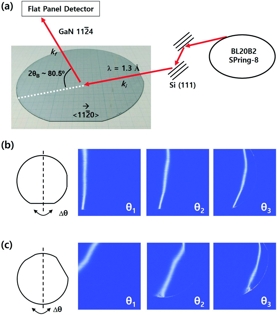 | ||
| Fig. 1 Experimental configuration for synchrotron X-ray diffraction topography on the 6 inch free-standing GaN substrate is described in (a). X-rays of 1.3 Å selected using a Si(111) monochromator were diffracted by the GaN(114) net planes at an angle of 2θB = 80.5°. The diffraction signals were recorded at various incident angles θ. The snapshots of the diffracted images at the azimuth angles of ϕ = 0° and ϕ = 120° are illustrated in (b) and (c), respectively. Due to the local anisotropic lattice plane bowing, the diffraction images are inclined, in the case of ϕ = 120°. | ||
Fig. 1(b) shows the experimental results at ϕ = 0° at various incident angles. The straight diffraction line moved toward the right direction because of the substrate bowing. This means that because of the lattice plane curvature, only some parts satisfy the Bragg condition showing a diffraction signal. If the angular step of sample rotation is too high or the Bragg peak is too sharp, some parts miss the Bragg condition, which shows a zebra-like pattern after the merging of the diffracted images, even though the crystallinity is high.37 To avoid this artefact, the size of the angular step can be decreased. Unlike at ϕ = 0°, the inclined diffraction peak was observed at ϕ = 120°. As the rotation angle increased, the diffraction image of the diagonal direction tended to move in the right direction. This feature indicates that the substrate bending is not spherical but anisotropically bowed.
Results and discussion
For the maximum intensity, peak position, and full width at half-maximum (FWHM), all the diffraction images were stacked after removing the background noise. The calculation was performed at all the pixel points in the image by sequential calculation. The diffraction images at various incident angles (θ) were stacked for the 3-dimensional matrix. By calculating the intensity distribution at each pixel point as a function of θ, we obtained the 2-dimensional peak intensity map, bending map evaluated from peak positions, and FWHM map.36Fig. 2(a) shows the reconstructed image obtained from the maximum intensity at ϕ = 0°. The bottom side of the substrate shows stronger maximum intensity than the substrate centre. Straight lines or dotted lines are artefacts from the image processing and dead pixels in the flat panel detector. In the case of the substrate top and right sides, large and complicated defect structures are seen. One interesting feature is a borderline between the substrate middle and bottom parts, which shows a curved structure. The radius of this borderline is larger than that of the 6 inch substrate, which may be from inhomogeneous growth. Dislocations might span over the substrate that formed such a huge arc. | ||
| Fig. 2 X-ray diffraction topography images obtained from the peak intensity at every point. The crystallinity in the substrate centre looks homogeneous, while the substrate edge parts show inhomogeneous intensities, which may be related to a high dislocation density. (a) Azimuth angles of ϕ = 0 and (b) ϕ = 120°. | ||
The diffraction intensity map at ϕ = 120° is almost the same as that at ϕ = 0° except the substrate edge, as illustrated in Fig. 2(b). This is because, at the substrate edge, the incident angle is almost normal to the m-plane and the X-rays illuminate the substrate notch. Therefore, the X-ray illuminated crystal volume is larger than other regions that show stronger X-ray diffraction intensity. However, in other positions, the incident angle is small with respect to the GaN(0001) net planes making diffraction intensity weak and sensitive to the surface. For these reasons, the diffraction intensity at the sample edge is higher than that in other places at a small incident angle.
To understand the lattice plane bending, we evaluated the rocking curve of all the pixel points. The rocking curve peak position map at ϕ = 0° is described in Fig. 3(a). The left side of the substrate has a lower value, and the peak position gradually increases as the position moves in the +x-direction, and the range of Δθ reached ∼0.8°. The derived radius of curvature from the cross-section along the broken black line was 11 m, as shown in Fig. 3(b). An abrupt increase of the Δθ was observed in the vicinity of the right-side edge (x ∼ 15 cm). It is known that the dislocation density near the seed crystal is high because of substrate bending.25 From this point of view, at x ∼ 15 cm, the dislocation density can be higher than that in other regions. The same analysis was done at ϕ = 120°, as shown in Fig. 3(c). The substrate bending was smaller than that at ϕ = 0°, which indicates anisotropic substrate bending, as shown in Fig. 1(c). The cross-section of the broken black line in Fig. 3(c) is depicted in Fig. 3(d). The Δθ was ∼0.6°, and the radius of curvature calculated over the relatively flat area from x = 2 to 13 cm was 34 m, much longer than that at ϕ = 0°. The drastic change of Δθ was observed at x ∼ 3 cm and 13 cm, which implies abrupt substrate bowing followed by the existence of high dislocation areas.
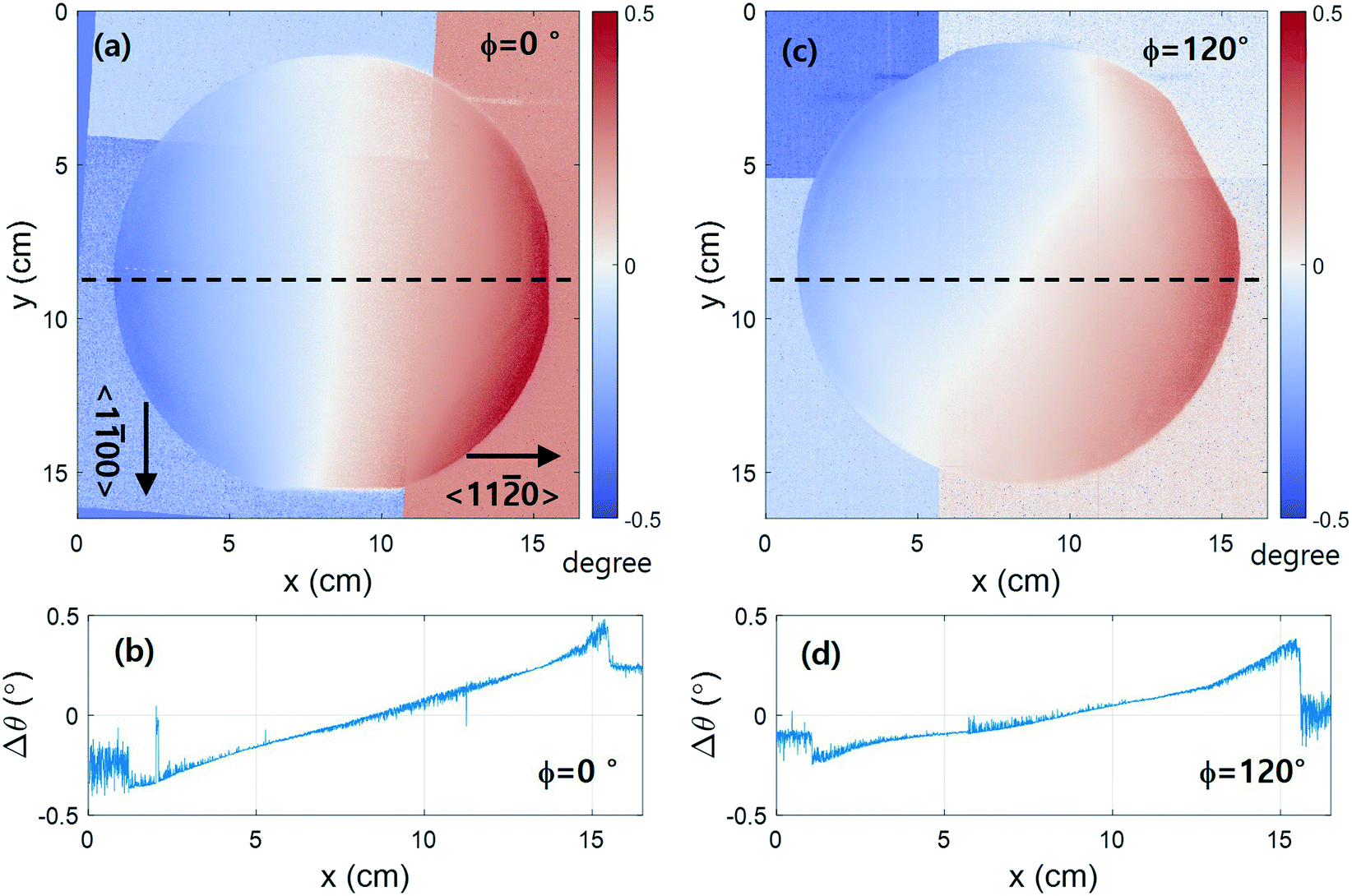 | ||
| Fig. 3 Lattice plane bending maps reconstructed from the peak position of the rocking curve. The substrate bending with a bending axis of [100] is observed in the case of ϕ = 0°, as shown in (a). A line profile in the middle of the substrate along the x-axis is described in (b). Lattice plane bending map at ϕ = 120° is illustrated in (c). The cross-sectional view along the broken black line is depicted in (d). | ||
The FWHM map of the 6 inch free-standing GaN at ϕ = 0° is illustrated in Fig. 4(a). Striped lines are seen along the [100] direction. The mean FWHM value evaluated over the substrate was 0.024°. The value at the substrate edge area at the top is higher than that in other places. Around the substrate bottom below the borderline, the FWHM is even smaller than that at the substrate centre, which indicates a localised higher crystalline area. We attribute this to the strain relaxation followed by dislocation formation. It is known that the strain of a free-standing GaN crystal is dependent on the GaN thickness on foreign substrates.38,39 Therefore, during the crystal growth or laser lift-off process, some parts in the substrate may be strained so that the substrate undergoes local deformation. Although the mechanism of this phenomenon remains unclear, it would be plausible for substrate bending and dislocation to provide an explanation, which may be related to the striped FWHM patterns. The same analysis was conducted at ϕ = 120°, as shown in Fig. 4(b). The overall features look similar, but the stripe patterns are inclined when compared with those at ϕ = 0°. The FWHM map does not change continuously on the borderline around the substrate bottom, which indicates that the substrate has already deformed along the boundary. If we assume that the crystal mosaicity comes from the threading dislocation, the dislocation density may be evaluated by the Burgers vector of the dislocation and the rocking curve width.40–42 However, according to a kinematical X-ray diffraction theory, the peak width is a function of the domain size. Moreover, the signal that we observe has already convolved with an instrumental resolution function. Therefore, the peak cannot be a delta function, even for the perfect crystal. In the case of high-quality GaN, it is difficult to estimate the dislocation density with the FWHM since several parameters such as crystallinity, dislocation density, and the instrumental resolution affect the X-ray rocking curve width.
 | ||
| Fig. 4 X-ray diffraction topography images reconstructed from the rocking curve width. The higher crystalline area (blue) and lower crystalline area (red) are distinguished with the borderline in the substrate bottom described in (a). The undulation of the FWHM along the X-ray direction of the substrate is seen at ϕ = 0°. In the case of ϕ = 120°, the stripe patterns are inclined, which is described in (b). | ||
To evaluate the 2-dimensional lattice plane tilting, we analysed the local q-vectors of GaN 114. The q-vector analysis method is described elsewhere.35,36 Two rotation matrices for the calculation of angular change of the q-vector were introduced. The projection of the q-vector to the (x, y)-plane is depicted in Fig. 5(a). In the vector plot, the arrow direction indicates 2-dimensional inclination with respect to the mean lattice plane bending angle. In particular, for the left and the right sides, the lattice plane significantly headed to the substrate centre. Interestingly, the substrate bending from top to bottom is much less than that in other directions. Fig. 5(b) shows the amplitude of the projected vector in Fig. 5(a), which shows cylindrical bowing.
 | ||
| Fig. 5 Lattice plane bending direction projected to the (x, y)-plane is described in (a). Symmetrical substrate bending with respect to the y-direction is observed. The degree of substrate bending was visualised from the magnitude of projected vectors (b). | ||
In the previous report on 4 inch free-standing GaN,35 the mean FWHM over the substrate was about 0.009°, which is about 3 times smaller than the current 6 inch substrate. However, the distribution of the FWHM map showed inhomogeneity originating from the nucleation sites, although the mean FWHM is small. In this respect, we can understand the inverse relationship between homogeneity and the distribution of the FWHM. In highly inhomogeneous cases, the area in the substrate can be separated into higher crystalline and lower crystalline regions, like the previous 4 inch case.35 However, for homogeneous cases, the mean FWHM of the rocking curve is higher than that of the inhomogeneous case. The role of GaN seeds is to minimize the strain originating from lattice mismatching during the ELO growth. In the case of a GaN crystal grown by seed-based methods, it shows a high dislocation density around the GaN seed but a low dislocation density away from the seed after the ELO growth. Therefore, the crystallinity became inhomogeneous over the wafer, in which the substrate is composed of two different areas. In our 6 inch GaN crystal, the overall crystallinity was slightly lower than that of other GaN crystals; however, the mean crystallinity was homogeneous.
Conclusions
6 inch free-standing GaN of high crystallinity was successfully grown using the Na-flux LPE method. X-ray diffraction topography, combined with a rocking curve imaging technique, showed huge boundaries between the high- and low-crystalline areas. Bending analysis showed that the lattice plane is anisotropically bowed along the [100] direction. The rocking curve width of GaN 114 averaged over the substrate was 0.024 ± 0.003°, which indicates a high crystallinity and homogeneous lattice plane over the substrate. We believe that there is a competition between substrate homogeneity and crystallinity.
Conflicts of interest
There are no conflicts of interest to declare.Acknowledgements
The measurements were performed at SPring-8 (Proposal No. 2020A1002, 2020A4503, 2020A4504, and 2020A1794) and SAGA-LS (Proposal No. 2001133S and 2007065S). This work was partly supported by the MEXT “Research and Development of Next-generation Semiconductor to Realize Energy-saving Society” (No. JPJ005357).References
- S. Nakamura, M. Senoh and T. Mukai, Jpn. J. Appl. Phys., 1993, 32, L8 CrossRef CAS.
- S. Nakamura, M. Senoh, N. Iwasa and S. Nagahama, Jpn. J. Appl. Phys., 1995, 34, L797 CrossRef CAS.
- N. Q. Zhang, S. Keller, G. Parish, S. Heikman, S. P. DenBaars and U. K. Mishra, IEEE Electron Device Lett., 2000, 21, 421 Search PubMed.
- W. Saito, Y. Takada, M. Kuraguchi, K. Tsuda, I. Omura, T. Ogura and H. Ohashi, IEEE Trans. Electron Devices, 2003, 50, 2528 CrossRef CAS.
- T. Takeuchi, H. Amano, K. Hiramatsu, N. Sawaki and I. Akasaki, J. Cryst. Growth, 1991, 115, 634 CrossRef CAS.
- M. E. Lin, S. Strite, A. Agarwal, A. Salvador, G. L. Zhou, N. Teraguchi, A. Rockett and H. Morkoç, Appl. Phys. Lett., 1993, 62, 702 CrossRef CAS.
- Y. Kato, S. Kitamura, K. Hiramatsu and N. Sawaki, J. Cryst. Growth, 1994, 144, 133 CrossRef CAS.
- K. Hiramatsu, S. Itoh, H. Amano, I. Akasaki, N. Kuwano, T. Shiraishi and K. Oki, J. Cryst. Growth, 1991, 115, 628 CrossRef CAS.
- S. Tomiya, T. Hino, S. Goto, M. Takeya and M. Ikeda, IEEE J. Sel. Top. Quantum Electron., 2004, 10, 1277 CrossRef CAS.
- F. A. Marino, N. Faralli, T. Palacios, D. K. Ferry, S. M. Goodnick and M. Saraniti, IEEE Trans. Electron Devices, 2010, 57, 353 CAS.
- F. A. Ponce, B. S. Krusor, J. S. Major Jr., W. E. Plano and D. F. Welch, Appl. Phys. Lett., 1995, 67, 410 CrossRef CAS.
- H. Amano, N. Sawaki, I. Akasaki and Y. Toyoda, Appl. Phys. Lett., 1986, 48, 353 CrossRef CAS.
- H. Amano, I. Akasaki, K. Hiramatsu, N. Koide and N. Sawaki, Thin Solid Films, 1988, 163, 415 CrossRef CAS.
- I. Akasaki, H. Amano, Y. Koide, K. Hiramatsu and N. Sawaki, J. Cryst. Growth, 1989, 98, 209 CrossRef CAS.
- Y. Tian, Y. Shao, Y. Wu, X. Hao, L. Zhang, Y. Dai and Q. Huo, Sci. Rep., 2015, 5, 10748 CrossRef CAS.
- S. S. Park, I. Park and S. H. Choh, Jpn. J. Appl. Phys., 2000, 39, L1141 CrossRef CAS.
- M. K. Kelly, R. P. Vaudo, V. M. Phanse, L. Görgens, O. Ambacher and M. Stutzmann, Jpn. J. Appl. Phys., 1999, 38, L217 CrossRef CAS.
- C. R. Miskys, M. K. Kelly, O. Ambacher and M. Stutzmann, Phys. Status Solidi C, 2003, 0, 1627 CrossRef CAS.
- K. Motoki, T. Okahisa, N. Matsumoto, M. Matsushima, H. Kimura, H. Kasai, K. Takemoto, K. Uematsu, T. Hirano and M. Nakayama, Jpn. J. Appl. Phys., 2001, 40, L140 CrossRef CAS.
- B. Beaumont, Ph. Vennéguès and P. Gibart, Phys. Status Solidi B, 2001, 227, 1 CrossRef CAS.
- C. Chu, F. Lai, J. Chu, C. Yu, C. Lin, H. Kuo and S. C. Wang, J. Appl. Phys., 2004, 95, 3916 CrossRef CAS.
- S. Porowski, MRS Internet J. Nitride Semicond. Res., 1999, 4, 27 CrossRef.
- K. Fujito, S. Kubo, H. Nagaoka, T. Mochizuki, H. Namita and S. Nagao, J. Cryst. Growth, 2009, 311, 3011 CrossRef CAS.
- H. Fujikura, T. Konno, T. Suzuki, T. Kitamura, T. Fujimoto and T. Yoshida, Jpn. J. Appl. Phys., 2018, 57, 065502 CrossRef.
- T. Hashimoto, F. Wu, J. S. Speck and S. Nakamura, Nat. Mater., 2007, 6, 568 CrossRef CAS.
- Y. Song, W. Wang, W. Yuan, X. Wu and X. Chen, J. Cryst. Growth, 2003, 247, 275 CrossRef CAS.
- X. L. Chen, Sci. Technol. Adv. Mater., 2005, 6, 766 CrossRef CAS.
- F. Kawamura, H. Umeda, M. Morishita, M. Kawahara, M. Yoshimura, Y. Mori, T. Sasaki and Y. Kitaoka, Jpn. J. Appl. Phys., 2006, 45, L1136 CrossRef CAS.
- Y. Mori, Y. Kitaoka, M. Imade, N. Miyoshi, M. Yoshimura and T. Sasaki, Phys. Status Solidi A, 2010, 207, 1283 CrossRef CAS.
- Y. Mori, Y. Kitaoka, M. Imade, N. Miyoshi, M. Yoshimura and T. Sasaki, Phys. Status Solidi C, 2011, 8, 1445 CrossRef CAS.
- Y. Mori, M. Imade, M. Maruyama and M. Yoshimura, ECS J. Solid State Sci. Technol., 2013, 2, N3068 CrossRef CAS.
- M. Imade, M. Imanishi, Y. Todoroki, H. Imabayashi, D. Matsuo, K. Murakami, H. Takazawa, A. Kitamoto, M. Maruyama, M. Yoshimura and Y. Mori, Appl. Phys. Express, 2014, 7, 035503 CrossRef.
- Y. Mori, M. Imanishi, K. Murakami and M. Yoshimura, Jpn. J. Appl. Phys., 2019, 58, SC0803 CrossRef CAS.
- Y. Mori, M. Imade, K. Murakami, H. Takazawa, H. Imabayashi, Y. Todoroki, K. Kitamoto, M. Maruyama, M. Yoshimura, Y. Kitaoka and T. Sasaki, J. Cryst. Growth, 2020, 350, 72 CrossRef.
- J. Kim, O. Seo, C. Song, Y. Chen, S. Hiroi, Y. Irokawa, T. Nabatame, Y. Koidea and O. Sakata, CrystEngComm, 2018, 20, 7761 RSC.
- J. Kim, O. Seo, C. Song, S. Hiroi, Y. Chen, Y. Irokawa, T. Nabatame, Y. Koide and O. Sakata, Appl. Phys. Express, 2018, 11, 081002 CrossRef.
- O. Seo, J. M. Kim, C. Song, Y. Lou, L. S. R. Kumara, S. Hiroi, Y. Chen, Y. Katsuya, Y. Irokawa, T. Nabatame, Y. Koide and O. Sakata, AIP Adv., 2018, 8, 075318 CrossRef.
- K. Yamane, T. Matsubara, T. Yamamoto, N. Okada, A. Wakahara and K. Tadatomo, J. Appl. Phys., 2016, 119, 045707 CrossRef.
- F. Lipski, M. Klein, X. Yao and F. Scholz, J. Cryst. Growth, 2012, 352, 235 CrossRef CAS.
- C. G. Dunn and E. F. Kogh, Acta Metall., 1957, 5, 548 CrossRef CAS.
- T. Metzger, R. Höpler, E. Born, O. Ambacher, M. Stutzmann, R. Stömmer, M. Schuster, H. Göbel, S. Christiansen, M. Albrecht and H. P. Strunk, Philos. Mag. A, 1998, 77, 1013 CAS.
- R. Chierchia, T. Böttcher, H. Heinke, S. Einfeldt, S. Figge and D. Hommel, J. Appl. Phys., 2003, 93, 8918 CrossRef CAS.
| This journal is © The Royal Society of Chemistry 2021 |