
Rapid fabrication of silver–cuprous oxide core–shell nanowires for visible light photocatalysts†
Siyi
Yan
,
Qiaohui
Yue
and
Jiangang
Ma
 *
*
Key Laboratory of UV-Emitting Materials and Technology, Ministry of Education, Northeast Normal University, Changchun, Jilin 130024, China. E-mail: majg@nenu.edu.cn
First published on 13th November 2020
Abstract
We report a new method that enables fabrication of Ag–Cu2O core–shell nanowires (NWs) by using pulsed ultraviolet laser light to irradiate a mixed aqueous copper acetate and Ag NW solution. Multiple experimental characterization techniques indicate that laser irradiation can induce both rapid (0.5–6 min) and controllable growth of Cu2O (20–150 nm) on the Ag NWs. Finite-difference time-domain simulations and mechanism analyses show that the good photocatalytic properties of the Ag–Cu2O core–shell NWs are related to the enhanced visible light absorption caused by localized surface plasmon resonance and the improved electron–hole separation efficiency caused by the Ag–Cu2O Schottky junction.
Cuprous oxide (Cu2O) is a typical p-type direct band gap semiconductor with low toxicity and abundant raw material reserves. Cu2O also has a high absorption coefficient in the visible light region, which is beneficial for the use of sunlight. These appealing material features mean that Cu2O has been widely used in fields including photocatalysis, photovoltaics and water splitting.1 In the past few decades, increasing awareness of environmental pollution problems has led to major progress in the design and performance improvement of Cu2O photocatalysts.2 The strategies used include increasing the specific surface area of the material via synthesis of Cu2O nanoparticles (NPs) or nanowires (NWs)3 and construction of heterostructures with metals, carbon-based nanomaterials, or metal oxide semiconductors.4 Among these approaches, the fabrication of metal–Cu2O core–shell (metal@Cu2O) nanostructures has been receiving ever-growing attention.5 These structures not only promote efficient charge separation and transfer, but also protect the metal cores from corrosion caused by reactants and the surrounding media. Silver offers advantages that include high conductivity, low cost, a tunable localized surface plasmon resonance (LSPR) frequency and a lattice mismatch of less than 4% with Cu2O, and thus is recognized as a highly efficient sensitizer that enhances the photocatalytic performance of Cu2O.6 Specifically, one-dimensional (1D) Ag@Cu2O NWs with high specific surface areas, fast and long-distance electron transfer properties and superior electron conductivity often present better photocatalytic performances than other geometries of this type.7 However, current Cu2O-based composite nanomaterials are generally prepared using solution-phase synthesis or electrochemical deposition methods.8 These methods face several issues, including their inevitable use of toxic reductants, high temperature and pressure requirements and very long processing times.
Conventional laser chemical method refers to the use of laser light to ablate solid targets in liquids for the synthesis of metastable phases and shapes.9 The advantages of this method include the simplicity of the operation, short experimental times and environmental friendliness. To date, however, laser chemical method has not been used to fabricate semiconductors from metal salt precursor solutions, to the best of our knowledge. Here, we demonstrate the possibility of rapid fabrication of Cu2O using a nanosecond-pulsed ultraviolet laser to irradiate an aqueous copper acetate solution for the first time. Compared with the conventional chemical synthesis methods which usually are time-consuming and strictly follow the thermal equilibrium conditions, the photochemical synthesis method proposed in this work is more convenient and efficient since the reaction can proceed in a few minutes at an ambient atmosphere and room temperature. Additionally, our method can have the advantages of LSPR effect of metal NWs and realize conformal deposition of metal oxide semiconductors on the metal NWs. We demonstrate that our method can be used to fabricate Ag@Cu2O NWs at room temperature in an atmospheric environment, and the morphology and thickness of the Cu2O shell can be controlled well by adjusting the laser irradiation time over a period of a few minutes. A combination of experimental characterization techniques and finite-difference time-domain (FDTD) simulations are used to analyze the structural and optical properties of the Ag@Cu2O NWs. These Ag@Cu2O NWs show better photocatalytic performance than the Cu2O NPs alone, which is attributed to the suppression of electron–hole recombination and enhancement of the light absorption through a LSPR process. The method developed in this work is anticipated to be capable of extension to the preparation of other metal@semiconductor heterostructures, which should be suitable for a diverse range of applications in optoelectronic devices.
Fig. 1 shows an illustration of the overall strategy used for wrapping of Cu2O on the Ag NWs. Briefly, the Ag NWs, copper acetate and a small amount of polyvinylpyrrolidone (PVP) were mixed in deionized water and stirred constantly to prepare the precursor solution. The precursor solution was then irradiated using a nanosecond pulsed laser with an operating wavelength of 248 nm. The duration of the laser irradiation process was 0.5–6 minutes. During laser irradiation, the photochemical reaction occurred and produced the Cu2O coatings on the Ag NW surfaces. The pure Cu2O NPs were prepared in the same way, with the only difference being that the Ag NWs were not added to the precursor solution. The experimental details are shown in the ESI.†
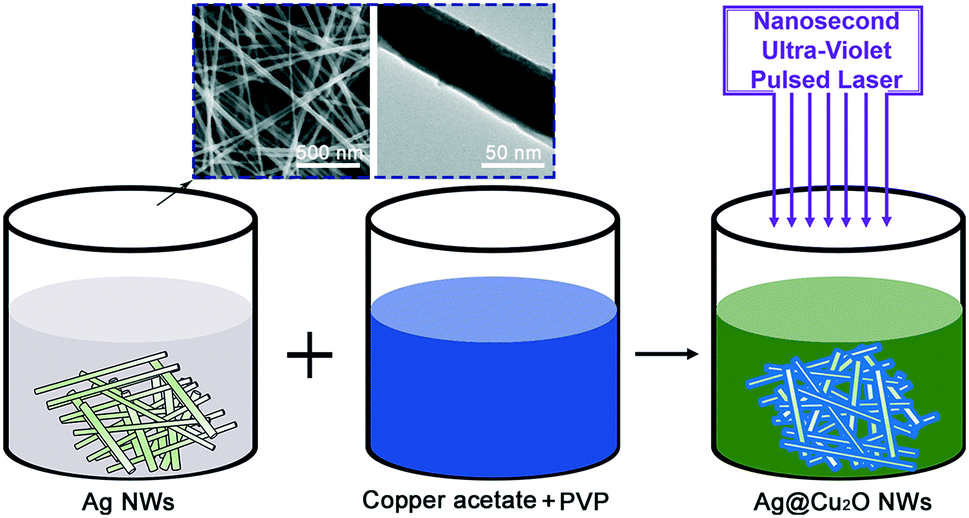 | ||
| Fig. 1 Schematic illustration of the process for the preparation of Ag@Cu2O NWs. Scanning electron microscopy (SEM) and transmission electron microscopy (TEM) images show the morphologies of the Ag NWs. | ||
Multiple experimental characterization techniques were performed to verify the formation of the Ag@Cu2O NWs. Fig. 2a shows a transmission electron microscopy (TEM) image of the NW produced. A shell layer with a thickness of approximately 10 nm that is composed of tiny NPs is shown on the NW surface. This should be attributed to the nucleation and growth of Cu2O NPs on the Ag@Cu2O NW surface. With the increasing laser irradiation time, the Cu2O shell will be thicker and it will continue further, and then the Cu2O NPs will be embedded into the as-formed Cu2O shell. The corresponding elemental mapping results are presented in Fig. 2b. The only elements observed are Cu, O, and Ag. The Ag is distributed strictly within the core region, while the Cu and O elements occupy wider areas than Ag in the radial direction. The high-resolution TEM image shown in Fig. 2c indicates that the interplanar spacing of the shell material is 0.308 nm, which corresponds to the (110) plane of face-centered cubic Cu2O. The interplanar spacing of the inner core material is 0.243 nm, which is consistent with the face-centered cubic Ag (111) plane. These results provide strong evidence that Cu2O is grown on the surfaces of the Ag NWs.
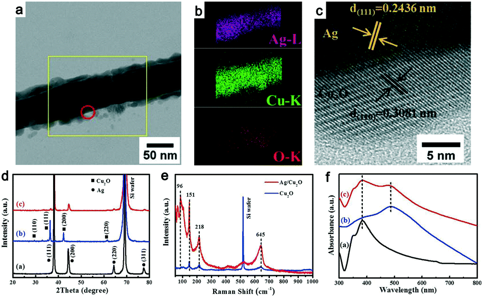 | ||
| Fig. 2 Morphological and structural characterization of the Ag@Cu2O NWs. (a) TEM image of the individual Ag@Cu2O NW. (b) Elemental mapping and (c) high-resolution TEM image of the Ag@Cu2O NW measured in the areas indicated by the yellow outline and the red circle, respectively. (d–f) X-ray diffraction (XRD) patterns, Raman spectra, and ultraviolet-visible (UV-vis) absorption spectra, respectively, of the Ag NWs (black lines), the Cu2O NPs (blue lines), and the Ag@Cu2O NWs (red lines). | ||
Fig. 2d shows the X-ray diffraction (XRD) patterns of the Ag NWs, the Cu2O NPs, and the Ag@Cu2O NWs. The XRD peaks in the black and blue lines can be indexed to face-centered cubic Ag (JCPDS #04-0783) and Cu2O (JCPDS #65-3288), respectively. The characteristic peaks of both Ag and Cu2O can be found in the XRD pattern of the Ag@Cu2O NWs and no diffraction peaks related to either Cu or CuO are observed. The XRD data agree well with the TEM results and thus confirm the formation of Ag@Cu2O NWs without impurities. Fig. 2e plots the Raman spectra of both the Cu2O NPs and the Ag@Cu2O NWs. The vibration peak shown at 218 cm−1 can be assigned to the second-order double-frequency of the 2Γ12− vibration mode.10 The peaks at 418 and 645 cm−1 are believed to be produced by multi-phonon processes and the infrared active vibration mode of Cu2O, respectively.11 The Raman vibration intensity of the Ag@Cu2O NWs is apparently stronger than that of the Cu2O NPs at the same wavenumber. This phenomenon can be ascribed to the Ag NWs, which act as antennas to collect the electric field. When compared with the Cu2O NPs, the Ag@Cu2O NWs exhibit a lower 151 to 96 cm−1 peak intensity ratio, thus indicating that the number of oxygen vacancy defects in the Ag@Cu2O NWs is lower than that in the Cu2O NPs.12
Fig. 2f shows the ultraviolet-visible (UV-vis) absorption spectra of the Ag NWs, the Cu2O NPs, and the Ag@Cu2O NWs. The aqueous Ag NW solution presents two absorption peaks at 350 and 385 nm. The former peak is attributed to the quadrupole resonance outside the plane of the Ag NWs, while the latter can be ascribed to Ag NW-related lateral plasma absorption.13 The Cu2O NPs show broad absorption at approximately 505 nm. This absorption wavelength matches the intrinsic band gap of Cu2O and is ascribed to inter-band optical transitions.14 The absorption spectrum of the Ag@Cu2O NWs shows two apparent absorption peaks that belong to the Ag NWs and Cu2O. When compared with pure Ag NWs, the lateral plasma absorption peak of the Ag@Cu2O NWs is broadened. This change is probably caused by the Cu2O cladding, which has a larger refractive index than the Ag NWs. The broadband absorption properties of the Ag@Cu2O NWs is essential for full utilization of incident sunlight.
The Cu2O morphology can be regulated by varying the concentrations of both PVP and the Ag NWs. PVP is a non-ionic polymer that is normally used as a surfactant in the synthesis of 1D nanomaterials. The long-chain PVP molecules adsorb preferentially on a specific crystal plane, changing the surface activity of the crystal material.15 To investigate the effect of PVP on the morphology of the Ag@Cu2O NWs, comparison experiments were performed using different PVP concentrations. The results show that increasing the PVP concentration to 2 mmol L−1 can suppress the agglomeration of the Cu2O nanocrystals, thereby promoting the formation of a smooth Cu2O shell on the Ag NWs (Fig. S1†). In contrast, the Ag NW concentration affects the nucleation of Cu2O (Fig. S2†). If the number of Ag NWs is low, then some of the Cu2O will form NPs rather than form the cladding on the Ag NWs. At a Ag NW concentration of 0.1 mg L−1, Ag@Cu2O NWs with uniform Cu2O shells are obtained. Further increases in the Ag NW concentration cause the Cu2O thickness to be thinner for the same reaction time.
The Cu2O thickness can be controlled easily by simply adjusting the laser irradiation time. For example, the surfaces of the Ag NWs are covered with a 20 nm-thick Cu2O layer (Fig. 3a and e) after a laser irradiation time of 0.5 min. There are also a small number of discrete Cu2O NPs on the Ag@Cu2O NWs. When the irradiation time is extended to 1 min, the Cu2O thickness increases to 50 nm and the Cu2O is wrapped around the Ag NWs uniformly (Fig. 3b and f). If the irradiation time is prolonged to 3 min, the Cu2O NPs may continue to grow and the Cu2O thickness becomes approximately 80 nm (Fig. 3c and g). A further increase in the irradiation time to 6 min sees the Cu2O thickness reaching up to approximately 150 nm and numerous octahedral Cu2O NPs are grown on the Ag NWs (Fig. 3d and h). These results clearly demonstrate that the Cu2O thickness can be controlled easily across the 20–150 nm range by adjusting the laser irradiation time over the 0.5–6 min range.
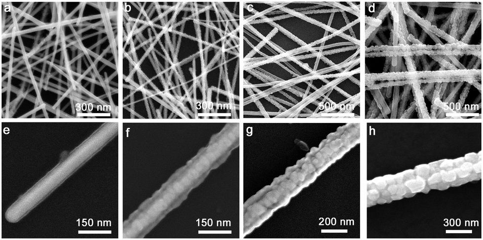 | ||
| Fig. 3 Ag@Cu2O NWs with a tunable Cu2O shell thickness. (a–d) SEM images of the Ag@Cu2O NWs and (e–h) the corresponding individual Ag@Cu2O NW prepared at laser irradiation times of 0.5, 1, 3, and 6 min. | ||
Based on the preparation condition-dependent surface morphology observations described above, the growth mechanism of Cu2O on the Ag NWs is proposed and is illustrated schematically in Fig. S3.† Briefly, the UV laser irradiation process causes a localized electric field enhancement at the surfaces of the Ag NWs and this near-field enhancement promotes a series of photochemical reactions that finally result in the production of Cu2O. The overall reaction equation is shown as follows:

FDTD theoretical simulations were conducted to provide physical insights into the far-field extinction and near-field enhancement processes of the Ag@Cu2O nanostructures with a core diameter of 50 nm and shell thicknesses of 20, 50, 80, 110 and 140 nm. Ag NWs are known to show strong LSPR absorption in the UV region and this absorption is sensitive to the environment surrounding the Ag NWs. In Fig. 4a, all the LSPR absorption peaks belonging to the Ag cores show progressive red-shifts with increasing Cu2O thickness. For example, the absorption spectrum of the Ag@Cu2O nanostructures with the 20 nm-thick Cu2O shell shows a characteristic LSPR absorption peak at approximately 510 nm. This absorption peak is red-shifted to approximately 850 nm when the Cu2O shell thickness is 140 nm. Another LSPR absorption peak of the Ag core moves from UV to the visible spectral region. This result is consistent with the results of previous observations of other metal–semiconductor core–shell nanostructures and is attributed to the high refractive index of Cu2O.16 Compared with the experimental absorption spectra of three-dimensional Ag@Cu2O NWs, the theoretically simulated absorption cross section of the two-dimensional Ag@Cu2O nanostructures exhibits a more obvious shift while increasing the Cu2O thickness. This phenomenon is reasonable and should be attributed to the amplification effect of the planar model.
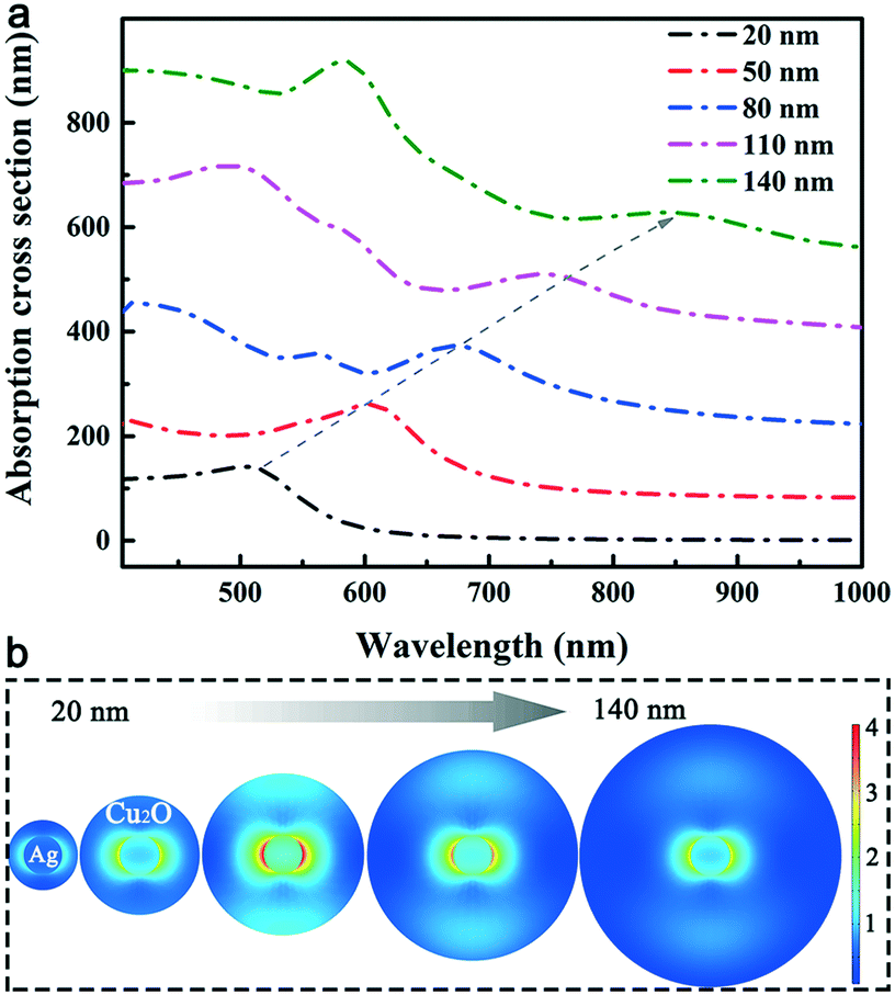 | ||
| Fig. 4 FDTD-simulated optical properties of Ag@Cu2O with various Cu2O thicknesses. (a) Calculated absorption cross-sections and (b) near-field distributions under 500 nm excitation of the Ag@Cu2O nanostructures. The Ag core diameter is 50 nm. The Cu2O thicknesses are 20, 50, 80, 110 and 140 nm. | ||
The FDTD-simulated near-field distributions of the Ag@Cu2O nanostructures at an incident light wavelength of 500 nm are shown in Fig. 4b. At a low Cu2O thickness of 20 nm, the electric field enhancement extends across the Cu2O shell to the outer surface of the core–shell nanostructure. The spatial confinement of the near-field enhancement increases with increasing Cu2O thickness and is maximized when the thickness is 80 nm. The electric field is also extended obviously over a long distance from the Ag core. The relatively small near-field enhancement at the low Cu2O thickness is attributed to the fact that the LSPR of the Ag core is damped slightly by the interband transitions of Cu2O. This damping is likely to be relieved as the Cu2O thickness increases up to 80 nm because the LSPR peak of the Ag@Cu2O nanostructures then shifts to longer wavelengths, at which the Cu2O shell will act as a dielectric layer.17 When the Cu2O thickness is increased further to 140 nm, the near-field enhancement is obviously weakened and almost all the electric field is then confined near the Ag core surface. These phenomena are probably related to the increases in the scattering and absorption cross-sections of the Cu2O shell layer, which hinder both the light incidence and the decoupling between the incident light and the red-shifted LSPR wavelength of the Ag cores. In addition, the near-field distributions of the Ag@Cu2O nanostructures at incident light wavelengths of 400 and 600 nm are shown in Fig. S4 in the ESI.† Different from the near-field distribution at 500 nm, the highest electric field enhancements occur at a Cu2O thickness of 50 and 110 nm while the wavelength of incident light is 400 and 600 nm, respectively. These phenomena are observed for the photoelectric conversion of Cu2O due to its large absorption coefficient over a broad range of light wavelengths.
The photocatalytic properties of the Ag NWs, the Cu2O NPs and the Ag@Cu2O NWs were evaluated via photodegradation of rhodamine B (RhB). The Ag@Cu2O NWs with the Cu2O shell thickness of 80 nm were used as the photocatalyst to ensure optimal degradation results. Fig. 5a and b show the absorption spectra of the RhB solutions after photocatalytic degradation over various times. The Ag@Cu2O NWs show better photocatalytic performance under visible light irradiation than the Cu2O NPs in terms of reducing the absorption of the RhB solution. Fig. 5c plots the degradation dynamic curves for these samples. No photodegradation occurs when only the Ag NWs are added to the RhB solution. Within 120 min, the Ag@Cu2O NWs and Cu2O NPs can decolor 79% and 34% of the RhB solution, respectively. Although the Ag@Cu2O NWs exhibit smaller specific surface area than the Cu2O NPs at the same weight, the photocatalytic activity of the former is still much higher than that of the latter, verifying that wrapping Ag NWs with a Cu2O shell is an effective strategy to improve the photocatalytic activity of Cu2O. The photocatalytic activity of our Ag@Cu2O NWs and various Ag–Cu2O composites were compared in the ESI† (Table S1).
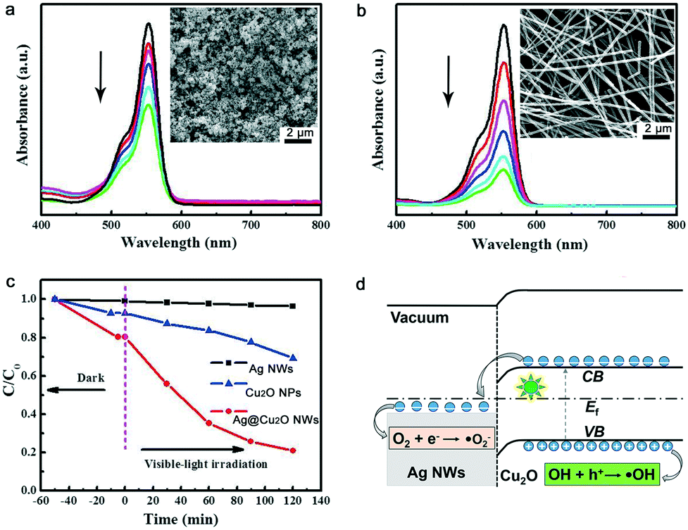 | ||
| Fig. 5 Photocatalytic properties and mechanism of the Ag@Cu2O NWs. Solar light irradiation time-dependent light absorption of RhB solutions in the presence of equal weights of the (a) Cu2O NPs and (b) Ag@Cu2O NWs acting as photocatalysts. (c) Photocatalytic degradation behavior of the RhB solutions when the Ag NWs, Cu2O NPs and Ag@Cu2O NWs are used as photocatalysts. (d) Schematic illustration of the charge separation process and photocatalytic mechanism of the Ag@Cu2O NWs under visible light irradiation. Here, Ef is the Fermi energy level, CB is the conduction band, and VB is the valence band. | ||
Based on the structural characteristics of the Ag@Cu2O NWs, the observed enhancement in the photocatalytic activity is mainly attributed to the synergistic effect of the Ag NW core and the Cu2O shell (Fig. 5d).18 On the one hand, a Schottky junction which can promote the separation of photogenerated electron–hole pairs should be formed at the Ag–Cu2O interface. In detail, the work function of the Ag NWs and the Fermi level of Cu2O are located at 4.4 and 4.8 eV, respectively, according to our Kelvin probe force microscopy measurements. The valence and conduction band positions of Cu2O are located at 4.2 and 6.4 eV, respectively.4 The free electrons generated by visible light illumination will be transferred from the Cu2O conduction band to the Ag NWs, and then on to the oxygen molecules. As a result, superoxide radical anions (˙O2−) that can decompose organic pollutants will be produced.19 The holes generated in the Cu2O valence band will be blocked by the Schottky barrier. They can produce hydroxyl radicals (˙OH), which plays an essential role in the oxidation decomposition of RhB.20 On the other hand, the Cu2O cladding promotes the LSPR wavelength of the Ag cores to red-shift to the visible light region, as evidenced by our FDTD simulations. At an optimal Cu2O thickness, the LSPR wavelength can match with the optical band gap of Cu2O. In this case, the light absorption of the Cu2O shells is enhanced and the numbers of photogenerated electrons and holes that are available to participate in the photocatalytic reactions will be increased. Therefore, the photocatalytic efficiency is obviously improved.
Conclusions
In summary, we have developed a method to fabricate Ag@Cu2O NWs using pulsed laser light to irradiate the mixed aqueous copper acetate and Ag NW solution. The morphology and the thickness of the Cu2O shell can be tuned by adjusting the laser irradiation time. The as-formed Ag@Cu2O NWs show better photocatalytic properties than the Cu2O NPs because of their LSPR-enhanced light absorption and the effective suppression of electron–hole recombination. The synthesis approach developed in this work has a wide-ranging process compatibility, thus making it an ideal method to perform further derivatizations and prepare core–shell heterostructures that combine metal NWs with a diverse range of metal oxide semiconductors. This potential range of one-dimensional heterostructures should find applications in the fields including energy generation, displays and lighting.The work is supported by the NSFC (no. 51872043, 51732003, 61574031, 51902049), “111 project” (no. B13013), and the Funds from Jilin Province (no. JJKH20190267KJ, 20200201076JC).
Conflicts of interest
There are no conflicts to declare.Notes and references
- J. Luo, L. Steier, M.-K. Son, M. Schreier, M. T. Mayer and M. Grätzel, Nano Lett., 2016, 16, 1848 CrossRef CAS; D. Barreca, G. Carraro, V. Gombac, A. Gasparotto, C. Maccato, P. Fornasiero and E. Tondello, Adv. Funct. Mater., 2011, 21, 2610 CrossRef; W.-C. Huang, L.-M. Lyu, Y.-C. Yang and M. H. Huang, J. Am. Chem. Soc., 2012, 134, 1261 CrossRef; R. Wick and S. D. Tilley, J. Phys. Chem. C, 2015, 119, 26243 CrossRef; A. Paracchino, V. Laporte, K. Sivula, M. Grätzel and E. Thismen, Nat. Mater., 2011, 10, 456 CrossRef; L. Guan, H. Pang, J. Wang, Q. Lu, J. Yin and F. Gao, Chem. Commun., 2010, 46, 7022 RSC; C. Ma, Z. Yang, W. Wang, M. Zhang, X. Hao, S. Zhu and S. Chen, J. Mater. Chem. C, 2020, 8, 2888 RSC.
- Y. A. Wu, I. Mcnulty, C. Liu, C. K. Lau, Q. Liu, A. P. Paulikas, C.-J. Sun, Z. Cai, J. R. Guest, Y. Ren, V. Stamenkovic, L. A. Curtiss, Y. Liu and T. Rajh, Nat. Energy, 2019, 4, 957 CrossRef CAS.
- Y. Tan, X. Xue, Q. Peng, H. Zhao, T. Wang and Y. Li, Nano Lett., 2007, 7, 3723 CrossRef CAS; C. Lu, L. Qi, J. Yang, X. Wang, D. Zhang, J. Xie and J. Ma, Adv. Mater., 2005, 17, 2562 CrossRef; Y. Chang and H. C. Zeng, Cryst. Growth Des., 2012, 4, 273 CrossRef; M. Pang and H. C. Zeng, Langmuir, 2010, 26, 5963 CrossRef; Y. Shang, D. Zhang and L. Guo, J. Mater. Chem., 2011, 22, 856 RSC.
- Y. Zhao, L. L. Fan, Y. Zhang, H. Zhao, X. Li, Y. Li, L. Wen, Z. Yan and Z. Huo, ACS Appl. Mater. Interfaces, 2015, 7, 16802 CrossRef CAS; C. Song, Z. Zhao, X. Sun, Y. Zhou, Y. Wang and D. Wang, Small, 2019, 15, 1804268 CrossRef; Q. Wei, Y. Wang, H. Qin, J. Wu, Y. Lu, H. Chi, F. Yang, B. Zhou, H. Yu and J. Liu, Appl. Catal., B, 2018, 227, 132 CrossRef; X. Han, X. He, L. Sun, X. Han, W. Zhan, J. Xu, X. Wang and J. Chen, ACS Catal., 2018, 8, 3348 CrossRef; C. Xu, L. Cao, S. Ge, W. Liu, H. Liu, Y. Yu and X. Qu, J. Hazard. Mater., 2010, 176, 807 CrossRef; J. Zhang, H. Ma and Z. Liu, Appl. Catal., B, 2017, 201, 84 CrossRef; Z. Wang, S. Zhao, S. Zhu, Y. Sun and M. Fang, CrystEngComm, 2011, 13, 2262 RSC; W. Zhou, D. Jiang, J. Xue and X. Li, CrystEngComm, 2019, 21, 30 RSC; M. A. Khan, Y. Wahab, R. Muhammad, M. Tahir and S. Sakrani, Appl. Surf. Sci., 2018, 435, 718 CrossRef.
- K. Awazu, M. Fujimaki, C. Rockstuhl, J. Tominaga, H. Murakami, Y. Ohki, N. Yoshida and T. Watanabe, J. Am. Chem. Soc., 2008, 130, 1676 CrossRef CAS; S.-H. Lee, S. W. Lee, T. Oh, S. H. Petrosko, C. A. Mirkin and J.-W. Jang, Nano Lett., 2018, 18, 109 CrossRef; X. Wan, J. Yang, X. Huang, S. Tie and S. Lan, J. Alloys Compd., 2019, 85, 398 CrossRef; A. K. Sasmal, J. Pal, R. Sahoo, P. Kartikeya, S. Dutta and T. Pal, J. Phys. Chem. C, 2016, 120, 21580 CrossRef; W. Zhang, X. Yang, Q. Zhu, K. Wang, J. Lu, M. Chen and Z. Yang, Ind. Eng. Chem. Res., 2014, 53, 16316 CrossRef; Y.-K. Lin, Y.-J. Chiang and Y.-J. Hsu, Sens. Actuators, B, 2014, 204, 190 CrossRef; S. Guo, Y. Wang, F. Zhang, R. Gao, M. Liu, L. Dong, Y. Liu, Y. Zhang and L. Chen, Nanomaterials, 2018, 8, 444 CrossRef; K. Mondal and A. Sharma, RSC Adv., 2016, 6, 83589 RSC; Z. Ai, L. Zhang, S. Lee and W. Ho, J. Phys. Chem. C, 2009, 113, 20896 CrossRef; S. Wei, J. Shi, H. Ren, J. Li and Z. Shao, J. Mol. Catal. A: Chem., 2013, 378, 109 CrossRef; C. H. Kuo, Y. C. Yang, S. Gwo and M. H. Huang, J. Am. Chem. Soc., 2011, 133, 1052 CrossRef.
- N. Meir, I. Jen-La Plante, K. Flomin, E. Chockler, B. Moshofsky, M. Diab, M. Volokh and T. Mokari, J. Mater. Chem. A, 2013, 1, 1763 RSC; J. Li, S. K. Cushing, J. Bright, F. Meng, T. R. Senty, P. Zheng, A. D. Bristow and N. Wu, ACS Catal., 2013, 3, 47 CrossRef CAS; B. Tahir, M. Tahir and N. A. S. Amin, Appl. Catal., B, 2019, 248, 167 CrossRef; M. Tahir and N. A. S. Amin, Int. J. Hydrogen Energy, 2017, 42, 11507 Search PubMed.
- C. Lee, K. Shin, Y. J. Lee, C. Jung and H. M. Lee, Catal. Today, 2018, 303, 313 CrossRef CAS; S. Yang, S. Zhang, H. Wang, H. Yu, Y. Fang and F. Peng, Mater. Res. Bull., 2015, 70, 296 CrossRef; Z. Xu, S. Ye, G. Zhang, W. Li, C. Gao, C. Shen and Q. Meng, J. Membr. Sci., 2016, 509, 83 CrossRef.
- B. Sciacca, S. A. Mann, F. D. Tichelaar, H. W. Zandbergen, M. A. van Huis and E. C. Garnett, Nano Lett., 2014, 14, 5891 CrossRef CAS; J. Xiong, Z. Li, J. Chen, S. Zhang, L. Wang and S. Dou, ACS Appl. Mater. Interfaces, 2014, 6, 15716 CrossRef; R. Bakthavatsalam and J. Kundu, CrystEngComm, 2017, 19, 1669 RSC.
- P. Liu, H. Cui, C. X. Wang and G. W. Yang, Phys. Chem. Chem. Phys., 2010, 12, 3942 RSC; J. Xiao, P. Liu, C. X. Wang and G. W. Yang, Prog. Mater. Sci., 2017, 87, 140 CrossRef CAS.
- T. Ha, J. P. Kim, I. Park, K. I. Sim, H. Lee, J.-S. Bae, S. J. Kim, T.-T. Kim, J. H. Kim, J. I. Jang and S.-Y. Jeong, APL Mater., 2019, 7, 031115 CrossRef.
- P. Dawson, M. M. Hargreave and G. R. Wilkinson, J. Phys. Chem. Solids, 1973, 34, 2201 CrossRef CAS.
- T. Sander, C. T. Reindl, M. Giar, B. Eifert, M. Heinemann, C. Heiliger and P. J. Klar, Phys. Rev. B: Condens. Matter Mater. Phys., 2014, 90, 045203 CrossRef.
- Y. B. Sun, B. Mayers and Y. Xia, Nano Lett., 2002, 2, 165 CrossRef CAS.
- P. Wang, M. Xi, L. Qin, S.-Z. Kang, Y. Fang and X. Li, ACS Appl. Nano Mater., 2019, 2, 7409 CrossRef CAS.
- D. Y. Kim, C. W. Kim, J. H. Sohn, K. J. Lee, M. H. Jung, M. G. Kim and Y. S. Kang, J. Phys. Chem. C, 2015, 119, 13350 CrossRef.
- G. Park, C. Lee, D. Seo and H. Song, Langmuir, 2012, 28, 9003 CrossRef CAS; L. Zhang, H. Jing, G. Boisvert, J. Z. He and H. Wang, ACS Nano, 2012, 6, 3514 CrossRef.
- H. Jing, N. Large, Q. Zhang and H. Wang, J. Phys. Chem. C, 2014, 118, 19948 CrossRef CAS.
- H. Wang, L. Zhang, Z. Chen, J. Hu, S. Li, Z. Wang, J. Liu and X. Wang, Chem. Soc. Rev., 2014, 43, 5234 RSC.
- Y. Pan, S. Deng, L. Polavarapu, N. Gao, P. Yuan, C. H. Sow and Q.-H. Xu, Langmuir, 2012, 28, 12304 CrossRef CAS.
- M. A. Khana, N. Nayana, M. K. Ahmada, S. C. Fhong and M. Tahir, Surf. Interfaces, 2020, 21, 100649 CrossRef.
Footnote |
| † Electronic supplementary information (ESI) available: SEM images, schematic illustration of the growth mechanism of Ag@Cu2O NWs, and the experimental section. See DOI: 10.1039/d0ce01430c |
| This journal is © The Royal Society of Chemistry 2021 |