
 Open Access Article
 This Open Access Article is licensed under a
 Creative Commons Attribution 3.0 Unported Licence
Ultrathin polymethylmethacrylate interlayers boost performance of hybrid tin halide perovskite solar cells†
Dong
Ding
,
Luis
Lanzetta‡
 ,
Xinxing
Liang‡
,
Ganghong
Min
,
Marcin
Giza
,
Thomas J.
Macdonald
and
Saif A.
Haque
*
,
Xinxing
Liang‡
,
Ganghong
Min
,
Marcin
Giza
,
Thomas J.
Macdonald
and
Saif A.
Haque
*
Department of Chemistry, Molecular Sciences Research Hub, Imperial College London, London W12 0BZ, UK. E-mail: s.a.haque@imperial.ac.uk
First published on 21st April 2021
Abstract
Introducing a polymethylmethacrylate (PMMA) layer at the (PEA)0.2(FA)0.8SnI3 perovskite/hole transport layer interface leads to a remarkable improvement in the photogenerated current density and fill factor, resulting in an increase in the power conversion efficiency from 6.5% to 10%. PMMA is proposed to mitigate interfacial charge losses and to induce a more favourable distribution of 2D perovskite phases, elucidating a pathway towards the development of high-performance tin-based perovskite solar cells.
Hybrid organic–inorganic perovskites have revolutionised photovoltaics with power conversion efficiencies (PCEs) in lead (Pb)-based perovskite solar cells achieving over 25%.1 However, toxicity and the relatively low operational stability remain as major challenges for Pb-based perovskite solar cells (Pb-PSCs).2,3 Whilst remarkable progress has been recently made in the area of device stability, the issue of Pb toxicity has yet to be solved. Hence, Pb-free materials have gained increasing attention as alternatives.4–6 Among these materials, tin halide perovskite solar cells (Sn-PSCs) are attractive due to their narrow bandgap and environmentally friendly elements.7,8 In particular, PSCs based on hybrid 2D/3D Sn-based absorber layers have been favoured due to their better stability and performance relative to their purely 3D counterparts.7,9–11 A number of strategies have been developed to improve the PCEs of Sn-PSCs, including the use of SnX2 additives, compositional engineering and surface passivation.12,13 Consequently, PCEs of Sn-PSCs have increased to more than 13%, which is the highest among Pb-free perovskite materials.12 In this communication, we introduce an alternative strategy to boost the PCE of Sn-PSCs based on the use of commodity polymer polymethylmethacrylate (PMMA) interlayers. PMMA has been used as a passivation material by a few groups in Pb-halide PSCs to reduce trap state density, improve film morphology and enhance device performance.14–17 PMMA was previously used as a passivation layer at the interfaces between perovskite and both electron and hole transport layers to mitigate defect-assisted recombination, leading to very high open-circuit voltages (Voc) and PCEs in Pb-based systems.14 Recently, inverted Pb-PSCs based on an inorganic nickel oxide (NiOx) hole transport layer (HTL) have demonstrated PMMA to be a beneficial additive in the NiOx precursor and also as an interlayer between the NiOx and perovskite.15,16 However, PMMA has not been coupled with polymer-based HTLs (such as PEDOT:PSS) in PSCs, while in Sn-PSCs it has only been applied as a perovskite precursor solution additive to passivate defects in the material. Hence, the effect of PMMA as an interfacial engineering layer is yet to be fully explored in Sn-PCSs.17 Herein, we introduce PMMA as an ultrathin interlayer at the PEDOT:PSS/perovskite interface to improve performance in p-i-n devices. Moreover, this easily implementable strategy provides a pathway to boost the PCE of Sn-PSCs. In this paper, we report the first Sn-PSC solar cell with the structure of ITO/PEDOT:PSS/PMMA/(PEA)0.2(FA)0.8SnI3/PCBM/BCP/Ag, achieving a PCE of 10.0%. The impact of the PMMA interlayer on device performance and microstructure of Sn-perovskite films has been investigated.
We fabricated a control device based on the following architecture: ITO/PEDOT:PSS/(PEA)0.2(FA)0.8SnI3/PCBM/BCP/Ag. For PMMA-based devices, the PMMA solution was dynamically spin coated onto an ITO/PEDOT:PSS electrode to form a PEDOT:PSS/PMMA heterojunction. The presence of PMMA layers was confirmed via water contact-angle measurements (Fig. S1, ESI†), showing the PMMA-based sample lower wetting (higher angle; 13.9° > 8.9°) due to the hydrophobic character of the polymer. The Sn perovskite film was deposited using a two-step spin coating method from a precursor solution comprising formamidinium iodide (FAI), SnI2, SnF2 and phenylethylammonium iodide (PEAI) in an N,N-dimethylformamide (DMF) and DMSO mixed solvent system.18 The formation of high-quality (PEA)0.2(FA)0.8SnI3 films was confirmed by UV-Visible spectroscopy and X-ray diffraction (XRD) as shown in Fig. S2a and b (ESI†) respectively. These data also indicate that the PMMA layer does not influence the absorption characteristics of the tin perovskite absorber layer. The (PEA)0.2(FA)0.8SnI3 devices were fabricated based on an inverted heterojunction solar cell architecture: ITO/PEDOT:PSS/PMMA/(PEA)0.2(FA)0.8SnI3/PCBM/BCP/Ag as depicted in Fig. 1a. Current density–voltage (J–V) curves of the best performing control and PMMA-based devices are shown in Fig. 1b. The control device yielded a PCE of 6.5% with open circuit voltage Voc = 0.60 V, short circuit current density Jsc = 16.2 mA cm−2 and fill factor FF = 0.67. Upon introduction of the PMMA interlayer at the PEDOT:PSS/perovskite interface, the PCE increased from 6.5% to 10%, which is an improvement of over 53%. This dramatic enhancement in PCE of the PMMA-based device can be mainly attributed to the high Jsc of 22.9 mA cm−2; this being an ∼40% improvement relative to the control device. We note that the PMMA-based device also exhibited an increased FF of 0.73. The integrated photocurrent densities of the control and PMMA-devices obtained from external quantum efficiency (EQE) in Fig. 1c are 16.0 and 22.5 mA cm−2 respectively, which closely match the Jsc values from J–V curves, further confirming the role of PMMA layer in improving the photocurrent density. As can be seen in Fig. 1c, the introduction of the PMMA layer within the device stack improves the EQE across the entire wavelength range (400 to 800 nm). The PMMA-based devices also showed high stability. Fig. 1d shows device performance of the PMMA-based solar cells biased at the maximum power point (MPP) voltage under continuous illumination. The PMMA-based Sn PSCs retained their initial performance after continuous operation for 70 min under one sun illumination. The PCE value increased slightly within the first 5 min of MPP operation, which is most likely due to a light-induced healing in the perovskite layer.19,20 To investigate the shelf stability of the perovskite solar cells, the PCE of PMMA-based device was measured 15 days after fabrication. During this time period, the devices were kept in an inert atmosphere under dark conditions. J–V curves measured on the day of fabrication and after 15 days are shown in Fig. 1d inset. The device shows a small increase in PCE with increasing storage time. This improvement may be attributed to self-healing or the release of crystal strain in the perovskite under dark conditions.21,22
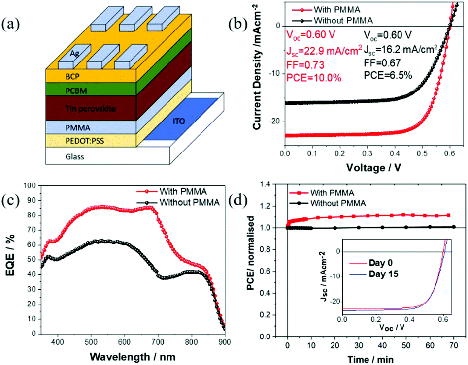 | ||
| Fig. 1 (a) Schematic drawing for the Sn-based halide perovskite solar cell comprising ITO/PEDOT:PSS/PMMA/(PEA)0.2(FA)0.8SnI3/PCBM/BCP/Ag. (b) J–V curves and (c) EQE curves of the (PEA)0.2(FA)0.8SnI3 perovskite solar cells with and without PMMA interlayer. (d) Normalised PCE of a high performance PMMA Sn perovskite device versus a control Sn perovskite device, operating at maximum power point (MPP) voltage under continuous illumination (100 mW cm−2) in a N2-filled atmosphere. (d) Inset shows J–V curves of the Sn-based perovskite solar cell with a PMMA layer as soon as fabricated and after 15 days. Day 0: PCE = 10.0%; day 15: PCE = 10.1%. | ||
In order to further verify the impact of the thin layer of PMMA on device performance, we fabricated 40 cells for both control and PMMA based solar cells. The box charts of each parameter (Jsc, FF & Voc) are shown in Fig. 2a–d. The PMMA devices show not only high values in each parameter but also great reproducibility relative to the control devices. Device performance statistics for both control and PMMA based solar cells are shown in Fig. S3 (ESI†).
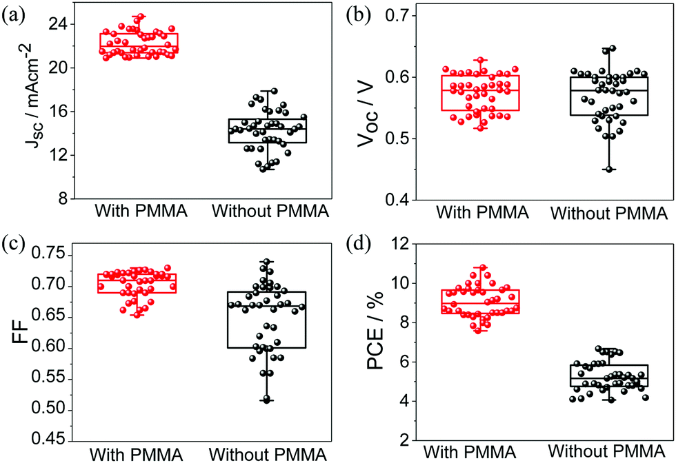 | ||
| Fig. 2 Box plots of the Sn perovskite solar cells metrics showing comparison of the (a) short-circuit current density, (b) open-circuit voltage, (c) fill factor and (d) PCE of the devices with PMMA (red) and without PMMA interlayer (black). | ||
It is pertinent to note that a strict control of the experimental procedures, including fabrication and testing, is essential to achieve the high device performance reported herein. First, the PMMA precursor (0.1 mg mL−1) was spin-coated dynamically at a fast speed (4000 rpm) with the aim of achieving a very thin layer, as we expect PMMA could either form an ultrathin layer where tunnelling effect is strongly dependent on the insulating layer thickness,23 or the carbonyl group on the PMMA could form a network and effectively passivate the perovskite at surface and its grain boundaries.14,24 Second, the fabrication process, including precursor preparation and film synthesis, as well as the testing procedure were carried out carefully in a nitrogen-filled environment to avoid rapid degradation of the Sn-PSC.
We now consider the possible origins of the improved device performance upon the addition of the PMMA interlayer. The increase in Jsc may be rationalised as follows. We studied the microstructure of the (PEA)0.2(FA)0.8SnI3 films with and without PMMA using scanning electron microscopy (SEM; Fig. 3a and b, respectively). Top-view images of the films reveal that their microstructures are similar. However, we note that the PMMA-based Sn perovskite film has slightly better coverage, possibly leading to improved crystallinity; this being consistent with the observed improvement in device performance reported herein. The almost identical absorption and PL characteristics of the perovskite films with and without PMMA interlayers as discussed earlier also suggest that the PMMA layer has negligible impact on the charge generation and separation, and the bulk properties of both samples are very similar. Fig. S4a (ESI†) presents steady-state PL and Fig. S4b (ESI†) presents time-resolved PL for Sn perovskite samples with and without the PMMA layer. Slightly longer fluorescence lifetime is observed in the PMMA sample (with PMMA: τ = 4.03 ns > without PMMA: τ = 3.52 ns); this being consistent with PMMA surface passivation (vide supra). We further hypothesise that the PMMA layer between PEDOT:PSS and Sn perovskite may allow photogenerated holes to tunnel through selectively while blocking electrons as illustrated in Fig. 3d; without the PMMA interlayer, electrons and holes are able to quickly recombine as shown in Fig. 3c. This is expected to reduce interfacial photocarrier recombination and is in agreement with the improvement in Jsc; a similar mechanism has been reported for insulating interlayers for lead-based perovskite solar cells.23 In support of this hypothesis, Lin et al. demonstrated that an ultra-thin layer of PMMA at the perovskite/ETL interface can enable charge injection into the perovskite via tunnelling.25,26 Furthermore, Fig. S5 (ESI†) presents steady-state PL for 2D (PEA)2(FA)n−1SnnI3n+1 Ruddlesden–Popper (RP) phases (where n is the number of octahedra sheets per 2D layer) in Sn perovskite samples with and without PMMA; a small increase in PL intensity in both sample sides (i.e. glass and film sides) is observed in the sample with PMMA, indicating a larger amount of 2D phases. This may be indicative of a more favourable 2D phase distribution in the film, allowing unrestricted charge transport in the perovskite layer and hence leading to the observed higher Jsc. The enhanced EQE in the PMMA-based cell (Fig. 1c) presents a new feature at ∼685 nm, which is attributed to the n = 2 RP phase. This further supports the role of 2D perovskite distribution in the increase of Jsc and device performance. We note that further detailed studies are underway to establish the exact mechanism by which PMMA improves device performance and will be reported in future work.
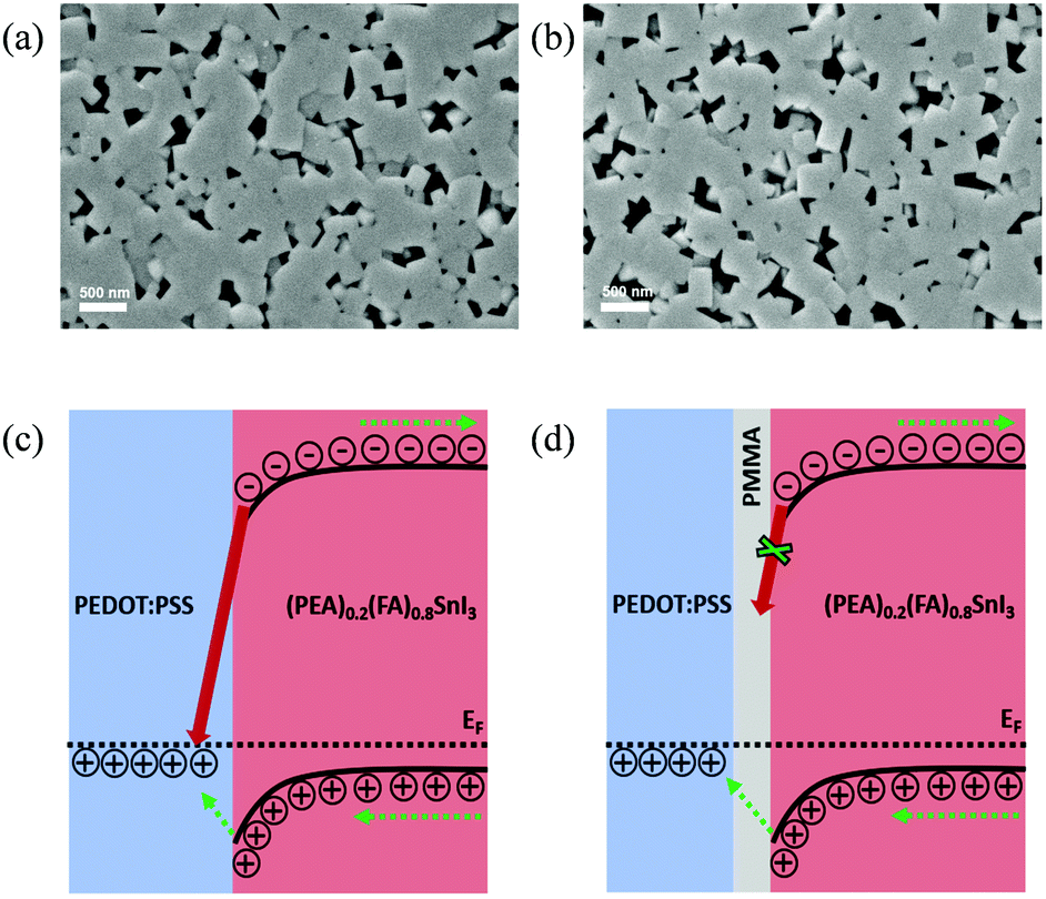 | ||
| Fig. 3 Top-view SEM image of (PEA)0.2(FA)0.8SnI3 films on top of (a) PMMA layer and (b) PEDOT:PSS layer. Scale bar denotes 500 nm. The schematic representation of the charge transfer between PEDOT:PSS and Sn perovskite layers (c) with PMMA interlayer suppressing the charge recombination, and (d) without PMMA layer. | ||
In summary, we fabricated 10.0% efficient (PEA)0.2(FA)0.8SnI3 perovskite solar cells with high reproducibility and we demonstrated that the insertion of an insulating PMMA layer at HTL/Sn-PSC interface could dramatically improve Jsc and FF. We note that our PMMA-based (PEA)0.2(FA)0.8SnI3 devices exhibited a ∼40% improvement in Jsc and, overall, a ∼53% increase in PCE relative to control solar cells. However, there is still room to improve the device performance, especially via increasing Voc. The work presented herein based on the use of ultrathin PMMA layers shows a promising, broadly applicable, and cost-effective direction towards the further development of highly efficient Sn-PSC solar cells.
Conflicts of interest
There are no conflicts to declare.Notes and references
- NREL Efficiency Chart.
- A. Abate, Joule, 2017, 1, 659–664 CrossRef CAS.
- J.-P. Correa-Baena, M. Saliba, T. Buonassisi, M. Grätzel, A. Abate, W. Tress and A. Hagfeldt, Science, 2017, 358, 739–744 CrossRef CAS PubMed.
- F. Bai, Y. Hu, Y. Hu, T. Qiu, X. Miao and S. Zhang, Sol. Energy Mater. Sol. Cells, 2018, 184, 15–21 CrossRef CAS.
- T. Krishnamoorthy, H. Ding, C. Yan, W. L. Leong, T. Baikie, Z. Zhang, M. Sherburne, S. Li, M. Asta, N. Mathews and S. G. Mhaisalkar, J. Mater. Chem. A, 2015, 3, 23829–23832 RSC.
- I. Turkevych, S. Kazaoui, E. Ito, T. Urano, K. Yamada, H. Tomiyasu, H. Yamagishi, M. Kondo and S. Aramaki, ChemSusChem, 2017, 10, 3754–3759 CrossRef CAS PubMed.
- L. Lanzetta, N. Aristidou and S. A. Haque, J. Phys. Chem. Lett., 2020, 11, 574–585 CrossRef CAS PubMed.
- J. Li, H.-L. Cao, W.-B. Jiao, Q. Wang, M. Wei, I. Cantone, J. Lü and A. Abate, Nat. Commun., 2020, 11, 310 CrossRef CAS PubMed.
- M. Li, W.-W. Zuo, Y.-G. Yang, M. H. Aldamasy, Q. Wang, S. H. T. Cruz, S.-L. Feng, M. Saliba, Z.-K. Wang and A. Abate, ACS Energy Lett., 2020, 5, 1923–1929 CrossRef CAS.
- E. Jokar, C.-H. Chien, C.-M. Tsai, A. Fathi and E. W.-G. Diau, Adv. Mater., 2018, 31, 1804835 CrossRef PubMed.
- L. Lanzetta, J. M. Marin-Beloqui, I. Sanchez-Molina, D. Ding and S. A. Haque, ACS Energy Lett., 2017, 2, 1662–1668 CrossRef CAS.
- K. Nishimura, M. A. Kamarudin, D. Hirotani, K. Hamada, Q. Shen, S. Iikubo, T. Minemoto, K. Yoshino and S. Hayase, Nano Energy, 2020, 74, 104858 CrossRef CAS.
- G. Liu, C. Liu, Z. Lin, J. Yang, Z. Huang, L. Tan and Y. Chen, ACS Appl. Mater. Interfaces, 2020, 12, 14049–14056 CrossRef CAS PubMed.
- J. Peng, J. I. Khan, W. Liu, E. Ugur, T. Duong, Y. Wu, H. Shen, K. Wang, H. Dang, E. Aydin, X. Yang, Y. Wan, K. J. Weber, K. R. Catchpole, F. Laquai, S. De Wolf and T. P. White, Adv. Energy Mater., 2018, 8, 1801208 CrossRef.
- G. Shen, H. Dong, Q. Cai, X. Wen, X. Xu and C. Mu, Sustainable Energy Fuels, 2020, 4, 3597–3603 RSC.
- X. Lian, J. Chen, S. Shan, G. Wu and H. Chen, ACS Appl. Mater. Interfaces, 2020, 12, 46340–46347 CrossRef CAS PubMed.
- L. Deng, K. Wang, H. Yang, H. Yu and B. Hu, J. Phys. D: Appl. Phys., 2018, 51, 475102 CrossRef.
- Y. Liao, H. Liu, W. Zhou, D. Yang, Y. Shang, Z. Shi, B. Li, X. Jiang, L. Zhang, L. N. Quan, R. Quintero-Bermudez, B. R. Sutherland, Q. Mi, E. H. Sargent and Z. Ning, J. Am. Chem. Soc., 2017, 139, 6693–6699 CrossRef CAS PubMed.
- W. Nie, J.-C. Blancon, A. J. Neukirch, K. Appavoo, H. Tsai, M. Chhowalla, M. A. Alam, M. Y. Sfeir, C. Katan, J. Even, S. Tretiak, J. J. Crochet, G. Gupta and A. D. Mohite, Nat. Commun., 2016, 7, 11574 CrossRef CAS PubMed.
- M. Saliba, M. Stolterfoht, C. M. Wolff, D. Neher and A. Abate, Joule, 2018, 2, 1019–1024 CrossRef CAS.
- E. Jokar, C.-H. Chien, A. Fathi, M. Rameez, Y.-H. Chang and E. W.-G. Diau, Energy Environ. Sci., 2018, 11, 2353–2362 RSC.
- C.-M. Tsai, Y.-P. Lin, M. K. Pola, S. Narra, E. Jokar, Y.-W. Yang and E. W.-G. Diau, ACS Energy Lett., 2018, 3, 2077–2085 CrossRef CAS.
- Q. Wang, Q. Dong, T. Li, A. Gruverman and J. Huang, Adv. Mater., 2016, 28, 6734–6739 CrossRef CAS PubMed.
- J. Jiang, J. Xu, H. Walter, A. Kazi, D. Wang, G. Wangila, M. Mortazavi, C. Yan and Q. Jiang, ES Mater. Manuf., 2020, 7, 25–33 CAS.
- K. Lin, J. Xing, L. N. Quan, F. P. G. de Arquer, X. Gong, J. Lu, L. Xie, W. Zhao, D. Zhang, C. Yan, W. Li, X. Liu, Y. Lu, J. Kirman, E. H. Sargent, Q. Xiong and Z. Wei, Nature, 2018, 562, 245–248 CrossRef CAS PubMed.
- X. Dai, Z. Zhang, Y. Jin, Y. Niu, H. Cao, X. Liang, L. Chen, J. Wang and X. Peng, Nature, 2014, 515, 96–99 CrossRef CAS PubMed.
Footnotes |
| † Electronic supplementary information (ESI) available: Experimental details, Fig. S1–S8. See DOI: 10.1039/d0cc07418g |
| ‡ These authors contributed equally. |
| This journal is © The Royal Society of Chemistry 2021 |