
 Open Access Article
 This Open Access Article is licensed under a Creative Commons Attribution-Non Commercial 3.0 Unported Licence
Near-field engineering for boosting the photoelectrochemical activity to a modal strong coupling structure†
Yanfeng
Cao
a,
Xu
Shi
 b,
Tomoya
Oshikiri
a,
Shuai
Zu
a,
Yuji
Sunaba
a,
Keiji
Sasaki
a and
Hiroaki
Misawa
*ac
b,
Tomoya
Oshikiri
a,
Shuai
Zu
a,
Yuji
Sunaba
a,
Keiji
Sasaki
a and
Hiroaki
Misawa
*ac
aResearch Institute for Electronic Science, Hokkaido University, Sapporo, Japan. E-mail: misawa@es.hokudai.ac.jp
bCreative Research Institution, Hokkaido University, Sapporo, Japan
cCenter for Emergent Functional Matter Science, National Chiao Tung University, Hsinchu, Taiwan
First published on 10th December 2020
Abstract
Near-field engineering is considered a significant strategy in constructing plasmonic nanostructures for efficient plasmonic chemistry. We demonstrate interfacial near-field engineering on a Au-NP/TiO2/Au-film (ATA) photoanode to improve the water oxidation efficiency. To tailor the near-field distribution, postdeposited Au on an ATA electrode (Au@ATA) is implemented using a facile constant potential electrolysis technique. As a result, the average photocurrent conversion efficiency of Au@ATA is approximately 1.3-fold higher than that of ATA.
Ultrahigh near-field enhancement is one of the most important properties in metallic nanostructures under the excitation of localized surface plasmon resonance (LSPR)1 and is widely demonstrated to play a crucial role in plasmonic chemical reactions.2 Especially in plasmonic electrochemical reactions, plasmon-induced electron transfer is known to enhance the visible light photoresponse of plasmonic metal nanoparticles deposited on typical n-type semiconductor electrodes.3 For the mechanism of electron transfer, it is considered that the hot electrons generated by the LSPR excitation transfer to the conduction band of the semiconductor, and the holes are captured in the surface states of the semiconductor and participate in the oxidation reaction. Because plasmon-induced hot-electron generation is strongly related to the nanoscale localization of the electromagnetic field near the metallic nanostructure,4 near-field engineering of the metallic nanostructures towards a strong and targeted near-field enhancement is very significant for photochemical and photocatalytic applications in which hot electrons play an important role.5
To date, many studies have focused on evaluating Au-NP/TiO2 systems because of their unique properties, such as plasmon-enhanced photocurrent generation and photocatalytic reactions in the visible region.6 Recently, we reported a photoanode constructed with Au-NP/TiO2/Au-film (ATA), which shows enhanced water oxidation quantum efficiency due to modal strong coupling between the Fabry–Pérot nanocavity mode of TiO2/Au-film and LSPR of Au-NPs.7 In the ATA structure, Au-NPs are partially inlaid 7 nm inside TiO2 thin film to increase the interaction between LSPR and the nanocavity. According to a finite element method (FEM) simulation, the hot spot of the near-field enhancement is located at the bottom interface of Au-NPs embedded into TiO2 (see Fig. 1), indicating that hot electrons/holes are generated and separated at the inlaid interface of Au-NPs/TiO2 inside TiO2. For the photochemical reaction, the holes must migrate to the surface of TiO2 to drive the water oxidation reaction. This migration process of holes has an adverse effect on the photochemical reaction because of the increase in possible recombination with electrons. Therefore, a strategy of near-field engineering to create a strong near-field enhancement near the interface of the three-phase boundary between Au-NPs, TiO2 and aqueous solution is in high demand for improving the water oxidation efficiency of the ATA structure.
 | ||
| Fig. 1 Near-field distribution under 650 nm irradiation calculated using an FEM simulation. Two near-field profile monitors were set in the xz- and xy-planes to visualize the near-field intensity, as shown by the blue and red dashed lines. (a) Simulation model, (b) side view (xz-plane), obtained by magnifying part of (a), and (c) top view (xy-plane) of ATA structures; (d) simulation model, (e) side view (xz-plane), obtained by magnifying part of (d), and (f) top view (xy-plane) of Au@ATA. The simulations were performed with a circularly polarized plane-wave light source in water. | ||
Morphology modulation is an efficient way to engineer the near-field spatial distribution on metallic nanostructures.8 Herein, we demonstrate a modulated ATA structure with electrochemically postdeposited Au, denoted as Au@ATA, in which the original Au-NPs are embraced by the postdeposited Au. The Au-NPs are partially inlaid in TiO2, which contributes to a strong light absorption similar to that of the original ATA structure. The postdeposited Au creates an interface between itself and TiO2 and thereby engineers the near-field spatial distribution on the surface of TiO2. Both parts should be indispensable to achieve high photoelectrochemical performances. The essential point of the morphology modulation is to selectively induce the near-field enhancement to the position near the three-phase boundary that is preferable for the water oxidation reaction.
Based on this concept, we first performed near-field simulations for the ideal models of ATA and Au@ATA structures. Fig. 1 shows the side views and top views of the near-field distributions of ATA and Au@ATA under irradiation of 650 nm as simulated by a commercial finite element solver (COMSOL Multiphysics®), in which E denotes the electric field amplitude. As shown in Fig. 1b and c, optical near fields with relatively high intensity are observed only at the Au-NP/TiO2 boundary inside TiO2. In contrast, for the Au@ATA structures, in addition to the strong near-field enhancement at the Au-NP/TiO2 boundary inside TiO2, a remarkable high-intensity near field at the edge of the interface between postdeposited Au and TiO2 is clearly apparent in Fig. 1e. Fig. 1f shows a more obvious near-field enhancement at the edge of the postdeposited Au despite the maximum of the scale bar of Fig. 1f being two orders of magnitude larger than that of Fig. 1c. Besides the ideal model of Au@ATA, we also performed the near-field simulations using other shapes of the postdeposited Au, as presented in Fig. S1e, f, h and i (ESI†). All the simulation results suggest that the postdeposited Au can effectively tailor the near-field intensity near the three-phase boundary of postdeposited Au, TiO2 and solution when the postdeposited Au creates an interface with the TiO2 even the Au structure shows an anisotropic shape. In contrast, near-field distribution does not change dramatically when the postdeposited Au just propagate on Au-NPs in z-direction (Fig. S1k and l, ESI†). This strong near-field enhancement at the interface of the postdeposited Au and TiO2 near the three-phase boundary is therefore expected to become primarily responsible for the efficient photochemical reaction.
According to the simulation results, we used a facile constant potential electrolysis (CPE) technique to postdeposit Au on an ATA electrode (Fig. S2, ESI†).9 The surface morphologies of ATA and Au@ATA were characterized via scanning electron microscopy (SEM). Fig. 2b–e displays typical top-view SEM images of ATA and Au@ATA structures with different reaction times. As displayed in Fig. S3a and c (ESI†), the average particle size of Au-NPs on ATA was estimated as 10 ± 6.7 nm. The surface morphology of ATA with an inlaid depth of 7 nm is shown in Fig. 2b. After electrodepositing Au on the ATA structure, as shown in Fig. 2c–e, the size of Au-NPs grew larger with increasing deposition time, indicating that the CPE method is successful and essential for electrodepositing Au. According to heterogeneous nucleation theory, the original Au-NPs on ATA structure can work as active centres to decrease the free energy of Au nucleating from the precursor solution,10 and the postdeposited Au prefers to be deposited on the original Au-NPs of the ATA structure. After appropriate deposition time such as 3 min, the postdeposited Au contact with the TiO2 surface. When the deposition time increased, the oversized Au nanostructure merges to neighbouring Au-NPs, and the more prominent anisotropic structure is formed. In addition, according to the particle number distributions calculated using SEM images shown in Fig. S4 (ESI†), the total number of Au-NPs on the ATA structure decreased after postdepositing Au. The faradaic efficiency was calculated as 82.4% from number of postdeposited Au atoms obtained from Fig. S4 (ESI†) and the amount of electric charge obtained in Fig. S5 (ESI†), indicating that the reductive current is consumed for the postdeposition of Au on the original Au-NPs.
 | ||
| Fig. 2 (a) Schematic process for electrochemically postdepositing Au on an ATA electrode (Au@ATA). Morphologies of Au@ATA with different deposition times. SEM images of (b) ATA (0 min), (c) Au@ATA with a 1 min deposition time, (d) Au@ATA with a 3 min deposition time, and (e) Au@ATA with an 8 min deposition time. (f and h) are the STEM image and EDX profile of ATA, respectively. (g and i) are the STEM image and EDX profile of Au@ATA with 3 min of deposition. The red and green colours depict TiO2 and Au, respectively. | ||
To observe the cross-section, characterization using scanning transmission electron microscopy (STEM) was performed, as shown in Fig. 2f and g. Before the postdeposition of Au, the Au-NP was partially inlaid as reported.7 After the postdeposition, the particle size of Au-NP was specifically increased on the top part of Au-NP, suggesting new Au was deposited on the original Au-NP. The energy-dispersive X-ray spectrometry (EDX) mapping in Fig. 2h and i further revealed the spatial configuration of Au-NPs and TiO2 layer. Fig. 2i clearly indicates that the postdeposited Au closely touches on the TiO2 surface and creates an interface. From a control experiment of depositing Pt on ATA using a similar CPE method (see Fig. S6, ESI†), we further determined that the postdeposited metal (Pt, Au) was intimately assembled on top of Au-NPs that were exposed to the aqueous solution. With regard to the surface morphology and the cross-section of the ATA and Au@ATA After electrodeposition, the original Au-NPs on the ATA structure were closely embraced by postdeposited Au. In these cases, it is expected that the near-field is enhanced at the interface of postdeposited Au and TiO2, as shown in Fig. 1e, f and Fig. S1e, f, h, i (ESI†).
To understand the effect of electrodeposited Au on the optical responses of ATA, we fabricated Au@ATA structures with different electrochemical deposition times (0–8 min) and compared the absorption spectra (Fig. 3a). The absorption spectra were obtained by measuring the transmittance T and reflectance R and calculating −log(T + R) as a function of wavelength. For all samples, absorption at wavelengths shorter than 500 nm can be primarily assigned to the interband transition of Au. At wavelengths longer than 550 nm, distinct dual bands were apparently observed, corresponding to the strong coupling-induced energy-level splitting into upper and lower modes.7 Additionally, the dual bands were almost maintained with increasing electrodeposition time of Au on the ATA structure. The absorption spectra were well reproduced using the peak fittings with three components (Fig. S7a, ESI†). The two components correspond to the upper and lower energy modes. The third component was also observed, which was considered to be the uncoupled Fabry–Pérot cavity mode, as reported.11 Also, all absorption spectra with different deposition time were plotted together for better comparison in Fig. S7b, ESI.† With increasing the deposition time, both absorption peaks of upper and lower modes shifted blue and the absorption intensity of lower energy mode decreased. The spectral changes are explained by the blue-shift of the LSPR band of Au-NPs due to the reduction of the inlaid ratio of Au nanostructure by high-refractive-index TiO2 (Fig. S7c, ESI†).
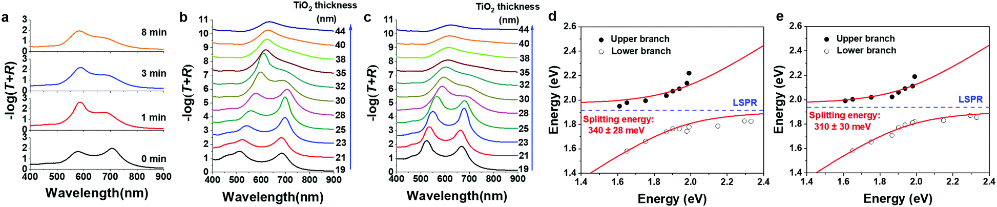 | ||
| Fig. 3 (a) Absorption spectra, calculated using −log(T + R), of the Au@ATA structures with varying electrochemical postdeposition times. The thickness of TiO2 was 28 nm. (b and c) are absorption spectra of ATA and Au@ATA structures, respectively, with various TiO2 thin-film thicknesses. (d and e) are dispersion curves of the splitting absorption band of ATA and Au@ATA, respectively. The red curves are the fittings using a coupled harmonic oscillator model. The blue dashed lines depict the LSPR energies of the Au NPs. | ||
To further understand the strong coupling properties of the ATA and Au@ATA structures, we fabricated ATA and Au@ATA structures with different TiO2 thicknesses (19–44 nm) and then measured their absorption spectra (Fig. 3b and c). For the ATA structure, the inlaid depth of Au-NPs was maintained at 7 nm. When the TiO2 thickness was thinner than 23 nm in both ATA and Au@ATA, the upper branch of the splitting absorption band was mainly affected by the interband transition of Au. As displayed in Fig. 3b, distinct dual bands were apparently observed at wavelengths longer than 550 nm, while the dual bands gradually disappeared and finally turned into an uncoupled LSPR band when the TiO2 thickness was greater.7 Nevertheless, after postdepositing Au on ATA structures, distinct dual bands were still apparently observed at wavelengths longer than 550 nm (Fig. 3c). The dispersion curves obtained by plotting the peak energy of the absorption spectra as a function of the energy of the cavity resonances are exhibited in Fig. 3d and e. The cavity resonance energies were obtained using the peak separation based on a Lorentz fitting because the cavity modes overlap the interband transition of Au occurring at wavelengths shorter than 500 nm. Using a coupled harmonic oscillator model,7 the splitting energies of ATA and Au@ATA were calculated to be 340 ± 28 meV and 310 ± 30 meV, respectively. Because the splitting energies of Au@ATA and ATA are very close, the strong coupling behaviour of Au@ATA is considered similar to that of ATA structures.7
Photoelectrochemical measurements were performed using a three-electrode system to evaluate the light-energy conversion efficiency (Fig. S8a, ESI†).12 Notably, there was no sacrificial electron donor in the electrolyte, and therefore water oxidation occurred. Fig. 4a shows the incident photon-to-current conversion efficiency (IPCE) action spectra of ATA and Au@ATA. The IPCE spectra were well reproduced using the peak fittings with two components, which correspond to the upper and lower energy modes (Fig. S8b, ESI†). Also, all IPCE action spectra with different deposition time were plotted together for better comparison in Fig. S8c, ESI.† After postdepositing Au on the ATA structures, the IPCE of Au@ATA in the wavelength region of 500–900 nm gradually increased as the deposition time increased up to 3 min. Interestingly, the maximum IPCE value of Au@ATA with a 3 min deposition reaches to approximately 2.5%. To study the possible mechanism underlying the IPCE enhancement of Au@ATA, we first considered the size effect of Au-NPs. After postdeposition, the average size of Au-NPs increases from 10 nm on ATA to 12 nm on Au@ATA. From the control experiment using ATA with large Au-NPs, as shown in Fig. S9, (ESI†), we concluded that the size increase is not the main contribution to the IPCE enhancement. Because photocurrent generation at wavelengths longer than 500 nm can be attributed to plasmon-induced charge separation at the Au-NP/TiO2 interface,6 the three-phase boundary between Au-NPs, TiO2 and aqueous solution plays an important role in the plasmon-induced water oxidation reaction. As discussed in Fig. 1, the IPCE enhancement should be assigned to the near-field enhancement at the three-phase boundary of Au-NPs, TiO2 and aqueous solution. On the ATA structure, the strong near-field enhancement is located at the boundary of Au-NP/TiO2 inside TiO2, where hot electrons/holes are generated. The holes must migrate to the surface of TiO2 to participate in the water oxidation reaction. Obviously, this migration process is disadvantageous because the recombination reaction with electrons might occur. After Au is electrochemically postdeposited on ATA to form Au@ATA, the near-field enhancement is tailored to the interface of postdeposited Au and TiO2 near the three-phase boundary, as shown in Fig. 1e, f and Fig. S1e, f, h, i (ESI†). Although the near-field enhancement is still high at the boundary of Au-NP/TiO2 inside TiO2, the generated holes at this position must migrate an even longer distance to participate the water oxidation reaction due to the postdeposited Au, which might not contribute to the IPCE enhancement. Thus, we can conclude that the tailored near-field enhancement at the interface of postdeposited Au and TiO2 near the three-phase boundary remarkably promotes the water oxidation reaction, resulting in an approximately 1.3-fold average IPCE enhancement compared to that of the ATA structure, as shown in Fig. 4b. This large IPCE enhancement is conducive to water oxidation in the visible region. When prolonging the deposition time to 8 min, oversized Au nanostructures were generated, resulting in reduced effective reaction interface. According to the calculation results from Fig. S4 (ESI†), the sum of the perimeter of the Au-NPs decreases from 4.1 × 10⁴ nm for 3 min of deposition to 3.1 × 10⁴ nm for 8 min of deposition. As a result, the water oxidation reaction of the 8 min deposition is repressed by a reduction of the three-phase boundary and oversized Au nanoparticles.8 In fact, the IPCE values are decreased by a factor of ∼1.9 compared to that for 3 min of deposition. Additionally, the IPCEs in the longer wavelength region is decreased due to the decrease of the absorption of the lower energy mode shown in Fig. 3a.
 | ||
| Fig. 4 (a) IPCE action spectra of Au@ATA photoelectrodes with different deposition times. (b) The corresponding average IPCE obtained from 500 nm to 900 nm. | ||
In summary, we have demonstrated a facile constant potential electrolysis technique for engineering the near-field distribution on ATA, which benefits plasmon-induced water oxidation. We found that Au was site-selectively postdeposited on the original Au-NPs of ATA. The near-field enhancement at the interface of postdeposited Au and TiO2 is crucial for boosting the photoelectrochemical activity. By comparing the photoelectrochemical activity of the Au@ATA electrode to that from ATA, an up to 1.3-fold higher average photocurrent conversion efficiency was observed from 500 nm to 900 nm. As a consequence, we can anticipate that this facile near-field engineering will lead to the development of more sophisticated photochemical systems, which can highly enhance the quantum yield of photochemical reactions, such as water splitting and carbon dioxide reduction. This work provides a facile and applicable approach to the further design of low-cost, feasible and prominent plasmon-enhanced energy conversion devices.
We are grateful to Ms Yuko Mori, Ms Naomi Hirai, and Prof. Yasutaka Matsuo at Hokkaido University for STEM measurements. We acknowledge the financial support from JSPS KAKENHI (Grant No. JP16H06506, JP18H03882, JP18H05205, JP18K05053, JP20H05083, and JP20K15113), the Nanotechnology Platform (Hokkaido University), and the Dynamic Alliance for Open Innovation Bridging Human, Environment and Materials (Five-Star Alliance) of MEXT.
Conflicts of interest
The authors declare there are no conflicts of interests.Notes and references
- (a) K. Li, N. J. Hogan, M. J. Kale, N. J. Halas, P. Nordlander and P. Christopher, Nano Lett., 2017, 17, 3710–3717 CrossRef CAS PubMed; (b) Y. L. Li, Q. Sun, S. Zu, X. Shi, Y. Q. Liu, X. Y. Hu, K. Ueno, Q. H. Gong and H. Misawa, Phys. Rev. Lett., 2020, 124, 163901 CrossRef CAS PubMed.
- (a) X. C. Ma, Y. Dai, L. Yu and B. B. Huang, Light: Sci. Appl., 2016, 5, e16017 CrossRef CAS PubMed; (b) K. Ueno, T. Oshikiri, Q. Sun, X. Shi and H. Misawa, Chem. Rev., 2018, 118, 2955–2993 CrossRef CAS PubMed; (c) M. Kauranen and A. V. Zayats, Nat. Photonics, 2012, 6, 737–748 CrossRef CAS.
- T. Oshikiri, K. Ueno and H. Misawa, Angew. Chem., Int. Ed., 2014, 53, 9802–9805 CrossRef CAS PubMed.
- (a) C. Clavero, Nat. Photonics, 2014, 8, 95–103 CrossRef CAS; (b) S. Linic, P. Christopher and D. B. Ingram, Nat. Mater., 2011, 10, 911–921 CrossRef CAS PubMed.
- (a) D. B. Ingram and S. Linic, J. Am. Chem. Soc., 2011, 133, 5202–5205 CrossRef CAS PubMed; (b) M. L. Brongersma, N. J. Halas and P. Nordlander, Nat. Nanotechnol., 2015, 10, 25–34 CrossRef CAS PubMed.
- (a) Y. Nishijima, K. Ueno, Y. Yokota, K. Murakoshi and H. Misawa, J. Phys. Chem. Lett., 2010, 1, 2031–2036 CrossRef CAS; (b) X. Shi, K. Ueno, N. Takabayashi and H. Misawa, J. Phys. Chem. C, 2013, 117, 2494–2499 CrossRef CAS; (c) X. Shi, X. W. Li, T. Toda, T. Oshikiri, K. Ueno, K. Suzuki, K. Murakoshi and H. Misawa, ACS Appl. Energy Mater., 2020, 3, 5675–5683 CrossRef CAS.
- X. Shi, K. Ueno, T. Oshikiri, Q. Sun, K. Sasaki and H. Misawa, Nat. Nanotechnol., 2018, 13, 953–958 CrossRef CAS PubMed.
- (a) K. L. Kelly, E. Coronado, L. L. Zhao and G. C. Schatz, J. Phys. Chem. B, 2003, 107, 668–677 CrossRef CAS; (b) P. Reineck, D. Brick, P. Mulvaney and U. Bach, J. Phys. Chem. Lett., 2016, 7, 4137–4141 CrossRef CAS PubMed.
- G. Gotti, K. Fajerwerg, D. Evrard and P. Gros, Electrochim. Acta, 2014, 128, 412–419 CrossRef CAS.
- N. T. K. Thanh, N. Maclean and S. Mahiddine, Chem. Rev., 2014, 114, 7610–7630 CrossRef CAS PubMed.
- (a) R. Chikkaraddy, B. Nijs, F. Benz, S. J. Barrow, O. A. Scherman, E. Rosta, A. Demetriadou, P. Fox, O. Hess and J. J. Baumberg, Nature, 2016, 535, 127–130 CrossRef CAS PubMed; (b) X. Xiong, J. B. You, P. Bai, C. E. Png, Z. K. Zhou and L. Wu, Nanophotonics, 2020, 9, 257–266 Search PubMed.
- Y. Nishijima, K. Ueno, Y. Yokota, K. Murakoshi, H. Inoue and H. Misawa, J. Phys. Chem. Lett., 2012, 3, 1248–1252 CrossRef CAS PubMed.
Footnote |
| † Electronic supplementary information (ESI) available. See DOI: 10.1039/d0cc07335k |
| This journal is © The Royal Society of Chemistry 2021 |