
 Open Access Article
 This Open Access Article is licensed under a
 Creative Commons Attribution 3.0 Unported Licence
Two-dimensional monoelemental germanene nanosheets: facile preparation and optoelectronic applications†
Chao
Li‡
 a,
Jianlong
Kang‡
a,
Jianlei
Xie‡
a,
Yingwei
Wang
*b,
Li
Zhou
b,
Haiguo
Hu
a,
Xinzhe
Li
a,
Jun
He
b,
Bing
Wang
*a and
Han
Zhang
a
a,
Jianlong
Kang‡
a,
Jianlei
Xie‡
a,
Yingwei
Wang
*b,
Li
Zhou
b,
Haiguo
Hu
a,
Xinzhe
Li
a,
Jun
He
b,
Bing
Wang
*a and
Han
Zhang
a
aInstitute of Microscale Optoelectronics, College of Physics and Optoelectronic Engineering, Collaborative Innovation Centre for Optoelectronic Science & Technology, Key Laboratory of Optoelectronic Devices and Systems of Ministry of Education and Guangdong Province, College of Physics and Optoelectronic Engineering, Shenzhen Key Laboratory of Micro-Nano Photonic Information Technology, Guangdong Laboratory of Artificial Intelligence and Digital Economy (SZ), Shenzhen University, Shenzhen 518060, P. R. China. E-mail: wangbing@szu.edu.cn
bHunan Key Laboratory for Super-microstructure and Ultrafast Process, School of Physics and Electronics, Central South University, 932 South Lushan Road, Changsha, Hunan 410083, People's Republic of China. E-mail: wyw1988@csu.edu.cn
First published on 24th September 2020
Abstract
Due to high carrier mobility, excellent stability, and tunable optical properties, 2D monoelemental germanene has attracted considerable attention in recent years. Herein, few-layered 2D germanium nanosheets (GeNS) were obtained via a facile liquid-phase exfoliated method and fabricated as electrode materials to assemble self-powered photo-electrochemical (PEC) type photodetectors. Such 2D GeNS-based PEC-type photodetectors exhibit a responsivity of 7.81 μA W−1, a detectivity of 5.2 × 10⁹ Jones, and the rise and decay times of 0.15 s and 0.76 s, respectively, under simulated light. At the specific wavelength of 380 nm, it demonstrates a responsivity of 340.91 μA W−1 and a detectivity of 1.82 × 10¹¹ Jones. In addition, the GeNS-based PEC-type device also exhibits good air-stability (over one-month). The present work demonstrates low-cost and facile fabrication techniques for preparing 2D monoelemental germanene and suggests that the as-prepared GeNS is a promising candidate for PEC-type photodetector applications.
1 Introduction
Photodetectors, kind of photo-electronic devices, can convert light signals to electrical signals and have a wide application in light-controlled switches, medical imaging, information communication, health monitoring, and display technology.1 Photodetectors greatly rely on the semiconductor materials, which have bandgaps and demonstrate light response due to the photoelectric effect. The early commercial materials for photodetectors are cadmium selenide and cadmium sulfide in the visible zone and lead sulfide in the invisible zone. In the mid-infrared zone, silicon, germanium, and HgCdTe with an adjustable bandgap dominate the markets at the moment. Group IVA elements are widely employed and still attract significant attention nowadays. For example, carbon materials own the merits of high carrier mobility, high stability, tunable optical properties, wide spectrum adsorption, and low cost. Besides, carbon materials possess numerous nanostructures such as zero-dimensional (0D) quantum dots (QDs), one-dimensional (1D) carbon nanotubes, and two-dimensional (2D) graphene. Carbon QDs can expand the spectral range from UV to infrared due to the quantum size effect.2–4 Tang et al.,5 demonstrated that N-GQDs exhibit broadband photoresponse from 365 to 980 nm due to extensive delocalized π electrons. Carbon nanotubes6 and graphene7 are also widely investigated. However, the detectivity of photodetectors based on pure carbon materials are far from satisfactory because of the limitation of light adsorption and ultrafast photocarrier recombination. Silicon, from the same main group, is dominating the electronics industry for decades and is suitable for detecting wavelengths shorter than 1.2 μm (near IR, visible, and UV) due to the indirect bandgap (1.12 eV). Traditional silicon thin films are obtained via the CVD method with high processing costs and a lack of mechanical rigidity. Similar to carbon materials, the solution processing method is easy to tailor the nanostructures of materials. Si QDs8 and Si NWs9 are developed as low cost and high-performance Si-based photodetectors. With a much smaller bandgap (0.67 eV) compared with silicon, the crystalline germanium (Ge)-based photodetector extend spectral range to the near-infrared zone.10 Siontas et al., reported Ge QDs embedded in an SiO2 matrix at a high temperature via photolithography.11 Such device shows a reduced leakage current with a consequently higher signal to noise ratio and improved photoresponse in a range of 400–1100 nm. Normally, the conventional Ge QD synthesis methods rely on the in situ growth formation accompanied by a high temperature (>700 °C) and sophisticated layer-by-layer processes (such as molecular beam epitaxy, high-temperature RF sputtering, and annealing).12 However, such a preparation process is time- and energy-consuming.In recent years, new series of photo-active semi-conductive materials, particularly 2D materials, such as transition metal dichalcogenides (TMDCs),13 topological insulators, phosphorene,14 perovskites,15 MXenes,16 and antimonene17 have attracted considerable attention.14,18–23 Some of 2D materials are experimentally and theoretically verified with specific merits, including tunable band structures, layer-dependent properties, high carrier mobility, and strong light absorption. Besides, 2D materials are more suitable for the solution processing method, which is a low-cost and high-yield fabrication method. Some typical compounds such as MoS2,24 InSe,25 Bi2S3,26 SnS,27 GeP,28 and single element materials, including Bi,29 Se,30 and Te,31 are well investigated as photo-detective materials by liquid-phase exfoliation method, followed by a liquid cascade centrifugation technique. Such a facile fabrication method and tunable size-controllable processes cost less and are more versatile. In 2009, Cahangirov et al., first predicted 2D germanium with stable and buckled honeycomb structures via first-principle calculations.32 Such a one-atom-thick germanium layer leads to fascinating electronic and magnetic properties, such as superconductivity. In 2014, Li et al., experimentally synthesized a 2D germanium sheet on a Pt(111) surface via the electron-beam evaporation method, followed by a high-temperature annealing process.33 Other (111) oriented metallic surfaces including Ag,34 Au,35 and Al36 are also suitable for the deposition of one Ge monolayer. Compared with liquid phase fabrication, such deposition method is unable to produce large quantities at a low cost. Goldberger et al., new hydrogen-terminated germanium (GeH) by the acid etching process of the topochemical deintercalation of CaGe2.37 The obtained GeH exhibited gram-scale and millimeter-sized crystallites. Due to acid etching, the termination with hydrogen atoms of such single- and few-layered 2D germanium sheets cannot be avoided.
Herein, we report few-layered 2D germanene nanosheets, which are obtained via a facile liquid-phase exfoliated method. Such 2D germanene nanosheets were well characterized and fabricated as electrode materials for PEC-type photodetector applications. In simulated light conditions, the PEC-type photodetector exhibits a responsivity of 7.81 μA W−1, a detectivity of 5.2 × 10⁹ Jones, and rise and decay times of 0.15 s and 0.76 s, respectively, at the condition of 0.6 V applied bias potential and under 0.5 M KOH electrolytes. At the wavelength of 380 nm, it manifests a responsivity of 340.91 μA W−1 and a detectivity of 1.82 × 10¹¹ Jones. The performance of GeNS-based device still preserves 73% of the original value even after one-month standing in air. The low-cost and facile fabrication techniques along with comparable photo-detective performances are well confirmed in this work.
2 Experimental
2.1 Materials
Bulk Ge crystals (99.999%) were purchased from Macklin Inc. N-Methyl-2-pyrrolidone (NMP, 99.5%) and poly(vinylidene fluoride) (PVDF, Mn = 71![[thin space (1/6-em)]](https://www.rsc.org/images/entities/char_2009.gif) 000 g mol−1) were purchased from Sigma Aldrich. ITO electrodes were bought from CSG Company.
000 g mol−1) were purchased from Sigma Aldrich. ITO electrodes were bought from CSG Company.
2.2 Preparation of 2D GeNS
In our case, a facile liquid-phase exfoliation method was conducted to obtain 2D monoelemental germanene nanosheets. In more detail, 30 mg Ge crystals were ground 30 min in an agate mortar and a small amount of an NMP solvent was added batch by batch several times. Then, small size Ge crystals were collected and subjected to a probe sonication at 300 W with an ON/OFF cycle of 4/2 s for 6 h under an Ar atmosphere. Previous theoretical investigations have evidenced that keeping the 2D materials away from water and oxygen can enhance the stability of the free-standing 2D material significantly.38,39 Before sonication, inert gases, such as argon, were constantly blown into the Ge NMP solution for a period to remove the oxygen in the solution. After that, the bottle was sealed to cut off the oxygen supply during the synthesis of the 2D material. Subsequently, the mixture was transferred to a 500 mL glass bottle with the NMP solvent in an ice bath ultrasound machine for a 12 h sonication. The 2D Ge nanosheets were obtained by a liquid cascade centrifugation (LCC) technique. The obtained 2D Ge nanosheet/NMP mixture was centrifuged at a speed of 6000 rpm for 5 min to remove the unexfoliated Ge crystals. The final 2D GeNS was obtained at a higher centrifugation speed of 12000 rpm for another 20 min.
2.3 Preparation of a 2D GeNS-based photodetector device
The obtained 2D Ge nanosheets were then re-dispersed in 1 mL of PVDF/DMF (10 mg/100 mL), followed by 30 min bath sonication (400 W). The PVDF/DMF solvent can continue to protect 2D GeNS from degradation. Then, the mixture was directly deposited on the surface of the ITO drop by drop and dried in a vacuum oven, and then the temperature of the oven was set to 60 °C for one night.The typical photoresponse behavior was evaluated using a PEC measurement system. A standard three-electrode system was built, consisting of a working electrode (2D Ge deposited on an ITO-coated glass substrate, photoanode), a counter electrode (platinum wire, photocathode), and a reference electrode (a saturated calomel electrode), and was tested in various aqueous electrolytes. An electrochemistry workstation CHI660E (CH Instruments, Inc., Shanghai) was used to control the bias potential and record the photocurrent generated. A 350 W Xenon arc lamp was placed 20 cm away from the reaction vessel and used as a light source. The illumination intensity on the photoanode was fixed at 100 mW cm−2. The linear sweep voltammograms of different samples were measured at a scan rate of 10 mV s−1. The EIS measurements were conducted at their open-circuit potential, with the frequency in the range of 100 kHz to 0.01 Hz and perturbation amplitude of 5 mV. All the experiments were carried out under the same conditions.
2.4 Characterization
Transmission electron microscopy (TEM, FEI Tecnai G2 F30) and atomic force microscopy (AFM, Bruker, Dimension ICON) were used to measure the morphology and thickness of the 2D Ge nanosheets. The Raman spectral analyses of the 2D Ge nanosheets and bulk Ge were performed using a high-resolution confocal Raman microscope (WITec alpha 300R) at 532 nm with a typical acquisition time of 5 ms per pixel in PL mapping. The Ge/NMP solutions for TEM, AFM, and Raman measurements were prepared using the following steps: the expected 2D Ge nanosheets were obtained by centrifugation and re-dispersed as solid precipitation in NMP. The optical absorption of the 2D Ge nanosheets was measured using a UV-vis-NIR spectrometer (Cary 60, Agilent). The X-ray photoelectron spectroscopy (XPS) characterization was carried out in a Thermo Fisher ESCALAB 250 Xi instrument with a monochromatic Al Kα X-ray source (1486.6 eV).3 Results and discussion
Ge nanosheets (GeNS) were prepared by a classical liquid-phase exfoliated method. To obtain the target morphology of germanium, the “cascade” centrifugation method was used to separate Ge nanosheets of different sizes after probe and ice-bath sonication in the NMP solvent. Fig. 1a shows a schematic for the fabrication of GeNS by liquid-phase exfoliation and liquid cascade centrifugation methods. The microscopic morphology of the GeNS structure was characterized via transmission electron microscopy (TEM), high-resolution TEM (HRTEM) as well as atomic force microscopy (AFM). As shown in Fig. 1b, the obtained TEM images exhibited that the average lateral size of GeNS was approximately one hundred nanometers. The inserted HRTEM image indicated the presence of distinct lattice fringes of 0.3485 nm, which is close to Ge (400) lattice parameters, with the contrast profiles of lattice fringe provided in Fig. S1 in ESM (ESI†). To confirm the element content of the as-prepared nanosheets, the scanning transmission electron microscopy (STEM) with energy dispersive Xray spectroscopy (EDS) mapping of elements was performed to obtain the element information. The results exhibited that Ge and O were well colocalized within its STEM microscopic morphology (Fig. 1c), and the O element content was relatively low. To note, vacancies, defects, and oxidation were inevitable during the preparation of the 2D material by the liquid-phase exfoliation method.40 They were the source of the ambient instability of the 2D material. The surface functionalization of germanene is an effective approach to further enhance its air stability.41 The TEM results suggest that the as-prepared GeNS possesses high-quality crystallization and excellent air stability. The thickness of the samples was determined to be as small as 5.9 nm, which was measured via atomic force microscopy (AFM), as shown in Fig. 1d. Fig. 1e depicts the ultraviolet-visible (UV-vis) spectra of the GeNS aqueous solution in which considerable broadband absorption range from 200 to 1400 nm can be observed. Furthermore, the Raman spectra of bulk Ge crystals and GeNS are shown in Fig. 1f. The Raman spectra exhibit prominent peaks at 296.8 cm−1, corresponding to the in-plane vibrations mode (E2g), which confirmed the crystalline structure of Ge.42 Compared to the bulk Ge powder, the in-plane vibrations mode (E2g) of GeNS underwent a redshift by 2 cm−1, further confirming the successful exfoliation of GeNS. The chemical constitution of GeNS was ascertained via X-ray photoelectron spectroscopy (XPS) (Fig. 1g). The binding energies of 3d5/2 and 3d3/2 doublets were located at 29.6 and 29.3 eV, respectively, which are consistent with the previously reported binding energies of the characteristic of Ge crystals.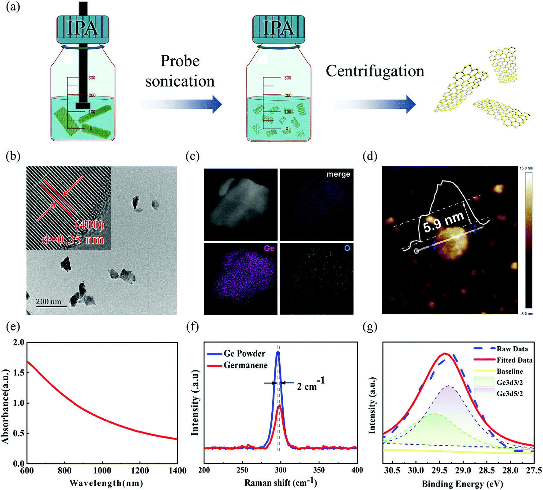 | ||
| Fig. 1 (a) The schematic of liquid-phase exfoliated for the preparation of 2D Ge nanosheets; (b) the TEM image with shape and HRTEM image with crystalline lattice of target GeNS; (c) the SEM images with its shape and corresponding elemental mapping images, including Ge, O elements and their merge; (d) the AFM image with thickness of GeNS; (e) the UV-Nis absorption spectrum of GeNS; (f) the Raman characteristic peak shift between Ge power and GeNS; (g) the XPS spectra of GeNS. | ||
The photo-response behaviors at different conditions were performed through a standard PEC-type photodetector having a three-electrode system. Due to the broadband absorption of GeNS, from ultraviolet to infrared, the photo-responses were tested in this range. To demonstrate the stability of GeNS, linear sweep voltammetry was conducted from −1 V to 1 V in KOH electrolytes (Fig. S2 in ESM, ESI†). The linear stable zone between 0–0.6 V proves that there were no electrochemical reactions in this voltage zone, and the fast-growing photocurrent between 0.6–1 V demonstrates the gain and loss electron of GeNS, which also shows the instability of GeNS at high voltage. To avoid the decomposition of GeNS, the voltages applied to the materials were limited to less than 0.6 V. To investigate the influences of voltage to PEC-type photodetector cell, three selected potential 0, 0.3, and 0.6 V were applied. In the condition of 0.5 M KOH electrolyte under simulated light (SL), 0.6 V voltage bias greatly promotes the separation of electrons and holes, therefore, showing larger photocurrents. The input light power density also has a large influence on the final performances. Six levels of light density from the dark state, Level I (26.2 mW cm−2), Level II (53 mW cm−2), Level III (83.1 mW cm−2), Level IV (118 mW cm−2) to Level VI (122 mW cm−2) were applied every 100 s with a light and dark statement rapid alterations every 5 s. The photocurrents were improved with the higher input light density in all three applied voltages. The exact quantitative photodetection performances can be expressed by the photocurrent density (Iph) and photoresponsivity (Rph), calculated by the equation given below:
| Iph = (Ilight − Idark)/S | (1) |
| Rph = Iph/Pλ | (2) |
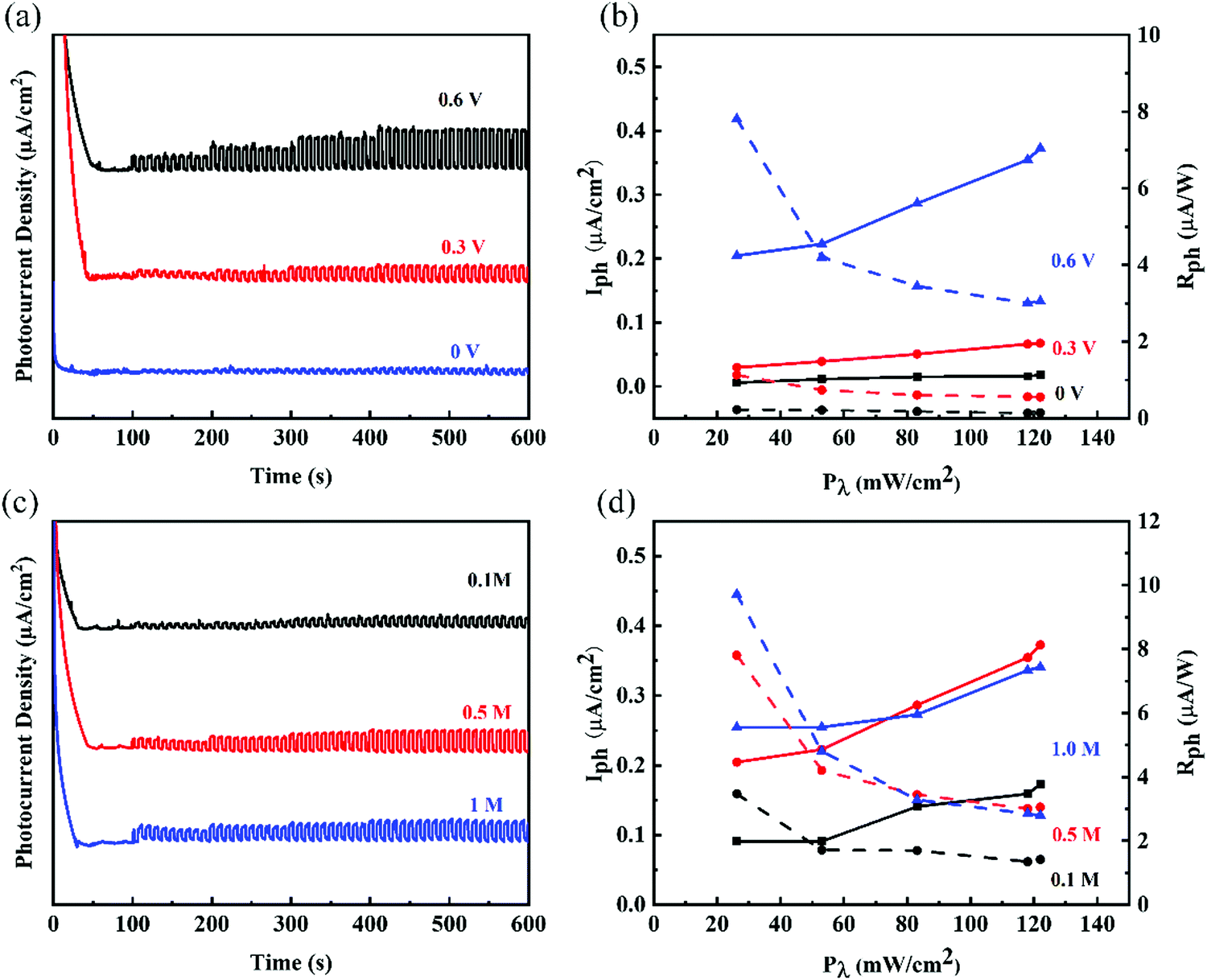 | ||
| Fig. 2 Typical photo-response behavior of the 2D GeNS-based photodetector triggered under simulated light and various conditions. (a) ON/OFF switching behavior with three selected applied potentials 0, 0.3, and 0.6 V at 0.5 M KOH electrolyte; (b) the corresponding calculated photocurrent densities (solid lines) and responsivity (dash lines) of (a); (c) ON/OFF switching behavior with three selected KOH concentration 0.1, 0.5, and 1 M KOH; (d) the corresponding calculated photocurrent densities (solid lines) and responsivity (dash lines) of (c). | ||
Another important experimental parameter that has a large influence on the final photodetector performances is the concentration of electrolyte. Fig. 2c shows the performances of the photodetector at three different concentrations (0.1, 0.5, and 1 M) of the KOH electrolyte and 0.6 V applied bias potential. Same as different applied potential, the photocurrents increased at a higher input light density in all three different concentrations. Among them, the performances of the photodetector in 0.1 M KOH electrolyte were lower than that of other two concentrations, while 0.5 M and 1 M showed comparable photodetective performances. As shown in Fig. 2d, a photocurrent of 0.09 μA cm2 and a photoresponsivity of 7.81 μA W−1 in 0.5 M KOH electrolyte were much larger than that in 0.1 M KOH electrolyte (0.20 μA cm2 and 3.5 μA W−1). The electrochemical impedance spectrum (EIS) is widely used to study the process dynamics and surface phenomena of the electrode, particularly contact resistance (Rs). The results demonstrate the resistance and the efficiency of charge transfer of the interface between the electrode and electrolyte. As shown in Fig. S3 in ESM (ESI†), comparable contact resistances in 0.5 M and 1 M KOH electrolytes were observed, with much larger interface resistance in 0.1 M KOH electrolytes.
To clearly show the exact photo-response wavelength, some typical wavelengths, including 350, 365, 380, 400, 475, 550, and 650 nm, were selected. The experiments were also conducted in three different concentrations of KOH electrolytes (0.1, 0.5, and 1 M). It demonstrates a similar concentration-performance relationship to that shown in simulated sunlight. However, the photocurrents in selected wavelengths were much smaller than that of simulated sunlight because of inefficient light irradiation. The more interesting phenomenon was higher photocurrent and photoresponsivity at the wavelengths of 365 nm and 380 nm. (Fig. 3) The highest photoresponsivity was 340.1 μA W−1 at 380 nm wavelength, 0.6 V applied bias potential, and 0.5 M KOH electrolyte. However, in the wavelength range from 380 nm to 650 nm, the photocurrent and photoresponsivity decreased gradually.
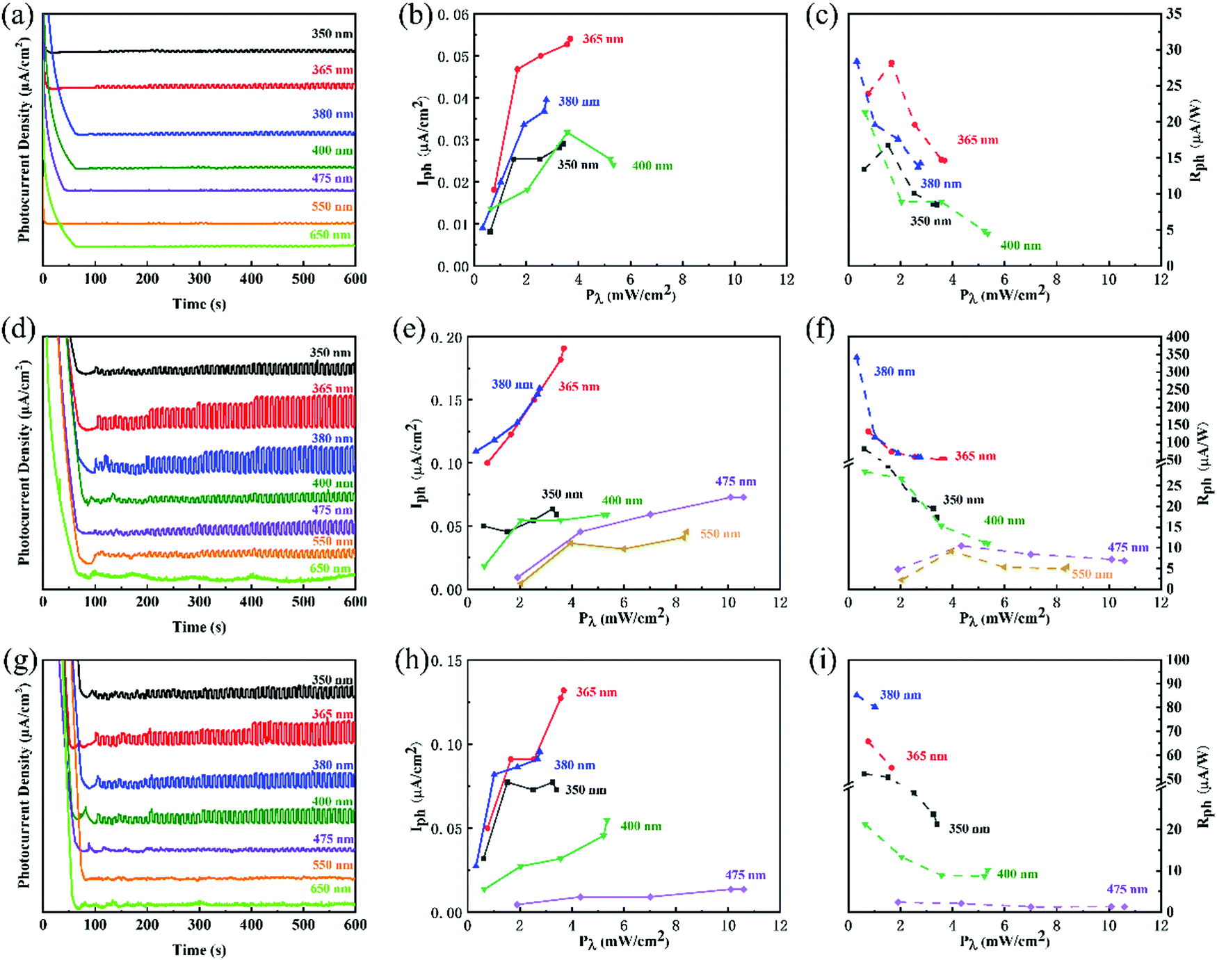 | ||
| Fig. 3 Typical photo-response behavior of the 2D GeNS-based photodetector with three selected KOH concentration of 0.1, 0.5, and 1 M KOH, at a voltage of 0.6 V under irradiation with wavelengths of 350, 365, 380, 400, 475, 550, and 650 nm; (a) ON/OFF switching behavior with a KOH concentration of 0.1 M KOH; (b) the calculated photocurrent density from (a); (c) calculated responsivity from (a); (d) ON/OFF switching behavior with a KOH concentration of 0.5 M KOH; (e) the calculated photocurrent density from (d); (f) the calculated responsivity from (d); (g) ON/OFF switching behavior with a KOH concentration of 1 M KOH; (h) the calculated photocurrent density from (g); (i) the calculated responsivity from (g). | ||
The detectivity (D*) is another important parameter, demonstrating the minimum detectable power of the illumination. The equation can be written as follows:
| D* = Rph × S1/2/(2q·Idark)1/2 | (3) |
Furthermore, the response time, including the rise time (trise) and recovery time (trec), of the 2D GeNS-based photodetector contributed to the 10% to 90% of interval time between the maximum photocurrent and dark current. Fig. 4a demonstrates the trise and trec of the photodetector in three different applied voltages. The best performance was a rise time of 0.15 s and a recovery time of 0.76 s for the 2D GeNS-based photodetector in 0.5 M KOH electrolyte and at 0.6 V applied voltage. This fast response can be attributed to the inherent high charge transportation of 2D GeNS. Fig. 4a also shows the much sluggish rise times and recovery times when less voltage was applied because the applied voltage helps in the separation and transportation of charge carriers. The long-term stability of materials is an important parameter for a photodetector. Therefore, the stability was tested for an extended time of 8000 s and a one-month interval time. Fig. 4b shows the steady photocurrent curves within 8000 s and after one-month standing without an obvious decay. The enlarged curves of photocurrents between 7500 s and 7600 s remain unchanged for fresh photodetector, while the curves started to collapse a little bit after one-month standing with the longer response time. The photocurrent still can maintain 73% after one-month standing, demonstrating good stability of the 2D GeNS material. The reduction in the photocurrent can be attributed to the decomposition of 2D GeNS, side electrochemical reaction of the 2D GeNS at a high bias voltage and electrode falling-off. Overall, the 2D GeNS-based photodetector shows good stability in alkaline electrolytes.
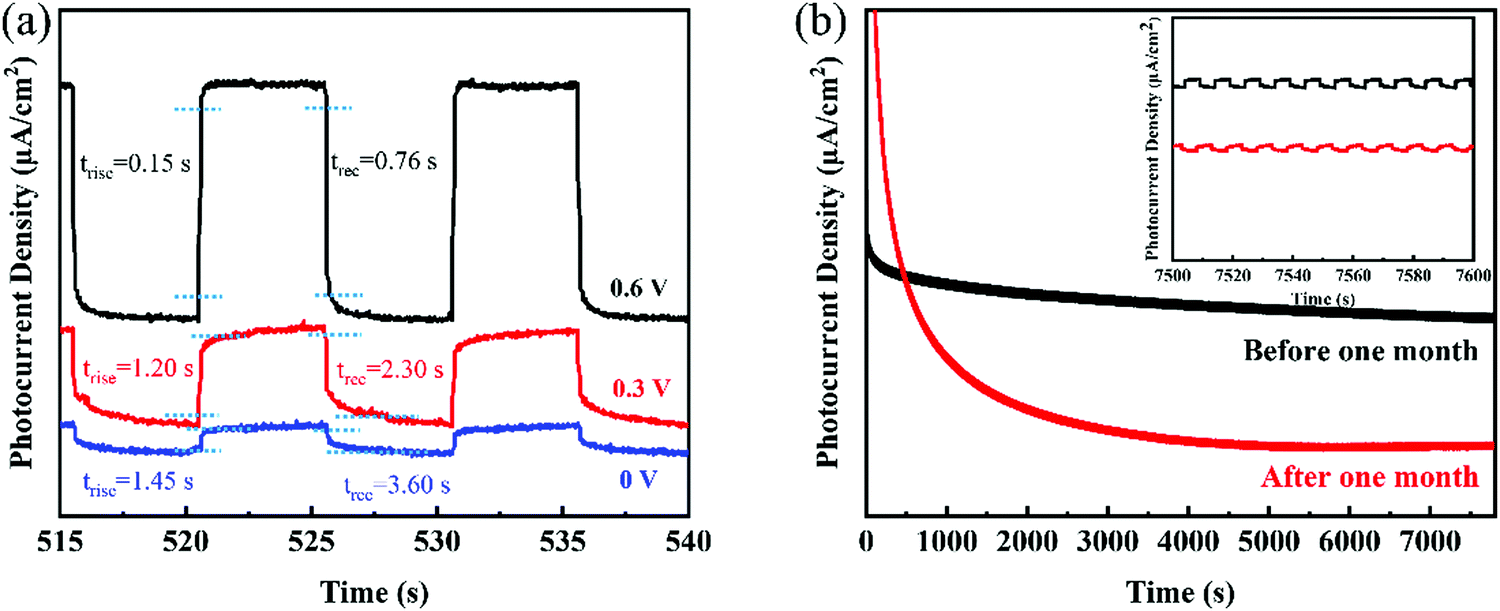 | ||
| Fig. 4 (a) The photocurrent density versus time for the rise (tris) and recovery (trec) times of the 2D GeNS-based photodetector with three applied voltages (0, 0.3 and 0.6 V). (b) Stability of photo-response behaviours of the 2D GeNS-based photodetector with 8000 s and one-month duration with 0.5 M KOH and at voltages of 0.6 V. (b) Enlarged 100 s cycles from 7500–7600 s. | ||
4 Conclusions
In conclusion, we reported a facile approach for obtaining 2D monoelemental germanene nanosheets and demonstrated a GeNS-based high-performance photodetector device. The comprehensive and detailed performance parameters of such photodetector device were well characterized. The photoresponsivity of 7.81 μA W−1 and a detectivity of 5.2 × 10⁹ Jones at 0.6 V applied voltage were achieved in 0.5 M KOH electrolyte. Such 2D GeNS-based photodetector devices show appreciable stability in alkaline solutions. Thus, the great merits of 2D GeNS nanosheets such as low-cost, environment-friendly, facile fabrication process, and suitable photodetection performances, proved that it has great potential in practical applications.Conflicts of interest
There are no conflicts of interest to declare.Acknowledgements
This research was supported by the National Natural Science Foundation of China (Grant No. 61874141; 11904239), Guangdong Natural Science Foundation of China (2019A1515010007), National Postdoctoral Program (2020M672782) and the Science and Technology Innovation Commission of Shenzhen (Grant No. JCYJ20170818141407343, JCYJ20190808175605495).References
- K. F. Mak and J. Shan, Nat. Photonics, 2016, 10, 216–226 CrossRef CAS
.
- X. Li, M. Rui, J. Song, Z. Shen and H. Zeng, Adv. Funct. Mater., 2015, 25, 4929–4947 CrossRef CAS
- C. Hu, M. Li, J. Qiu and Y.-P. Sun, Chem. Soc. Rev., 2019, 2315–2337 RSC
- H. J. W. Li, K. Huang and Y. Zhang, Mater. Res. Express, 2019, 6, 045902 CrossRef
- L. Tang, R. Ji, X. Li, G. Bai, C. P. Liu, J. Hao, J. Lin, H. Jiang, K. S. Teng, Z. Yang and S. P. Lau, ACS Nano, 2014, 8, 6312–6320 CrossRef CAS
- S. Pyo, J. Choi and J. Kim, Adv. Electron. Mater., 2019, 5, 1800737 CrossRef
- G. Y. Jiang, N. Zheng, X. Chen, G. Y. Ding, Y. H. Li, F. G. Sun and Y. S. Li, Chem. Eng. J., 2019, 373, 1309–1318 CrossRef CAS
- T. Yu, F. Wang, Y. Xu, L. Ma, X. Pi and D. Yang, Adv. Mater., 2016, 28, 4912–4919 CrossRef CAS
- E. Mulazimoglu, S. Coskun, M. Gunoven, B. Butun, E. Ozbay, R. Turan and H. E. Unalan, Appl. Phys. Lett., 2013, 103, 083114 CrossRef
- L. Tang, S. E. Kocabas, S. Latif, A. K. Okyay, D.-S. Ly-Gagnon, K. C. Saraswat and D. A. B. Miller, Nat. Photonics, 2008, 2, 226–229 CrossRef CAS
- S. Siontas, P. Liu, A. Zaslavsky and D. Pacifici, Appl. Phys. Lett., 2016, 109, 053508 CrossRef
- X. Liu, X. Ji, M. Liu, N. Liu, Z. Tao, Q. Dai, L. Wei, C. Li, X. Zhang and B. Wang, ACS Appl. Mater. Interfaces, 2015, 7, 2452–2458 CrossRef CAS
- B. Wang, S. P. Zhong, Z. B. Zhang, Z. Q. Zheng, Y. P. Zhang and H. Zhang, Appl. Mater. Today, 2019, 15, 115–138 CrossRef
- X. Ren, Z. Li, Z. Huang, D. Sang, H. Qiao, X. Qi, J. Li, J. Zhong and H. Zhang, Adv. Funct. Mater., 2017, 27, 1606834 CrossRef
- X. Qi, Y. Zhang, Q. Ou, S. T. Ha, C.-W. Qiu, H. Zhang, Y.-B. Cheng, Q. Xiong and Q. Bao, Small, 2018, 14, 1800682 CrossRef
- L. Wu, X. Jiang, J. Zhao, W. Liang, Z. Li, W. Huang, Z. Lin, Y. Wang, F. Zhang, S. Lu, Y. Xiang, S. Xu, J. Li and H. Zhang, Laser Photonics Rev., 2018, 12, 1800215 CrossRef
- W. Huang, Y. Zhang, Q. You, P. Huang, Y. Wang, Z. N. Huang, Y. Ge, L. Wu, Z. Dong, X. Dai, Y. Xiang, J. Li, X. Zhang and H. Zhang, Small, 2019, 15, e1900902 CrossRef
- J. Wang, K. Wang, Z. Yang, X. Li, J. Gao, J. He, N. Wang, H. Wang, Y. Zhang and C. Huang, ACS Sustainable Chem. Eng., 2020, 8, 1741–1750 CrossRef CAS
- W. Huang, C. Li, L. Gao, Y. Zhang, Y. Wang, Z. N. Huang, T. Chen, L. Hu and H. Zhang, J. Mater. Chem. C, 2020, 8, 1172–1197 RSC
- Z. Guo, H. Zhang, S. Lu, Z. Wang, S. Tang, J. Shao, Z. Sun, H. Xie, H. Wang, X.-F. Yu and P. K. Chu, Adv. Funct. Mater., 2015, 25, 6996–7002 CrossRef CAS
- Z. Guo, S. Chen, Z. Wang, Z. Yang, F. Liu, Y. Xu, J. Wang, Y. Yi, H. Zhang, L. Liao, P. K. Chu and X.-F. Yu, Adv. Mater., 2017, 29, 1703811 CrossRef
- C. Xing, W. Huang, Z. Xie, J. Zhao, D. Ma, T. Fan, W. Liang, Y. Ge, B. Dong, J. Li and H. Zhang, ACS Photonics, 2018, 5, 621–629 CrossRef CAS
- B. Wang, S. Zhong, Y. Ge, H. Wang, X. Luo and H. Zhang, Nano Res., 2020, 13, 891–918 CrossRef CAS
- N. Liu, P. Kim, J. H. Kim, J. H. Ye, S. Kim and C. J. Lee, ACS Nano, 2014, 8, 6902–6910 CrossRef CAS
- J. Lee, R. H. Kim, S. Yu, D. B. Velusamy, H. Lee, C. Park, S. M. Cho, B. Jeong, H. S. Kang and C. Park, 2D Mater., 2017, 4, 9 Search PubMed
- W. Huang, C. Xing, Y. Wang, Z. Li, L. Wu, D. Ma, X. Dai, Y. Xiang, J. Li, D. Fan and H. Zhang, Nanoscale, 2018, 10, 2404–2412 RSC
- W. Huang, Z. Xie, T. Fan, J. Li, Y. Wang, L. Wu, D. Ma, Z. Li, Y. Ge, Z. N. Huang, X. Dai, Y. Xiang, J. Li, X. Zhu and H. Zhang, J. Mater. Chem. C, 2018, 6, 9582–9593 RSC
- C. Li, J. Guo, Y. Zhang, J. Kang, W. Huang, T. Zhai and H. Zhang, J. Mater. Chem. C, 2020, 16, 5547–5553 RSC
- H. Huang, X. Ren, Z. Li, H. Wang, Z. Huang, H. Qiao, P. Tang, J. Zhao, W. Liang, Y. Ge, J. Liu, J. Li, X. Qi and H. Zhang, Nanotechnology, 2018, 29, 235201 CrossRef
- T. Fan, Z. Xie, W. Huang, Z. Li and H. Zhang, Nanotechnology, 2019, 30, 114002 CrossRef CAS
- Z. J. Xie, C. Y. Xing, W. C. Huang, T. J. Fan, Z. J. Li, J. L. Zhao, Y. J. Xiang, Z. N. Guo, J. Q. Li, Z. G. Yang, B. Q. Dong, J. L. Qu, D. Y. Fan and H. Zhang, Adv. Funct. Mater., 2018, 28, 1705833 CrossRef
- S. Cahangirov, M. Topsakal, E. Akturk, H. Sahin and S. Ciraci, Phys. Rev. Lett., 2009, 102, 236804 CrossRef CAS
- L. Li, S. Z. Lu, J. Pan, Z. Qin, Y. Q. Wang, Y. Wang, G. Y. Cao, S. Du and H. J. Gao, Adv. Mater., 2014, 26, 4820–4824 CrossRef CAS
- H. Oughaddou, S. Sawaya, J. Goniakowski, B. Aufray, G. Le Lay, J. M. Gay, G. Tréglia, J. P. Bibérian, N. Barrett, C. Guillot, A. Mayne and G. Dujardin, Phys. Rev. B: Condens. Matter Mater. Phys., 2000, 62, 16653–16656 CrossRef CAS
- M. E. Dávila, L. Xian, S. Cahangirov, A. Rubio and G. Le Lay, New J. Phys., 2014, 16, 095002 CrossRef
- M. Derivaz, D. Dentel, R. Stephan, M.-C. Hanf, A. Mehdaoui, P. Sonnet and C. Pirri, Nano Lett., 2015, 15, 2510–2516 CrossRef CAS
- E. Bianco, S. Butler, S. Jiang, O. D. Restrepo, W. Windl and J. E. Goldberger, ACS Nano, 2013, 7, 4414–4421 CrossRef CAS
- S. Barraza-Lopez and T. P. Kaloni, ACS Cent. Sci., 2018, 4, 1436–1446 CrossRef CAS
- T. P. Kaloni, K. Chang, B. J. Miller, Q.-K. Xue, X. Chen, S.-H. Ji, S. S. P. Parkin and S. Barraza-Lopez, Phys. Rev. B: Condens. Matter Mater. Phys., 2019, 99, 134108 CrossRef CAS
- S. Zhang, S. Guo, Z. Chen, Y. Wang, H. Gao, J. Gomez-Herrero, P. Ares, F. Zamora, Z. Zhu and H. Zeng, Chem. Soc. Rev., 2018, 47, 982–1021 RSC
- T. Maric, S. M. Beladi-Mousavi, B. Khezri, J. Sturala, M. Z. M. Nasir, R. D. Webster, Z. Sofer and M. Pumera, Small, 2020, 16, e1902365 CrossRef
- J. Ouyang, C. Feng, X. Ji, L. Li, H. K. Gutti, N. Y. Kim, D. Artzi, A. Xie, N. Kong, Y. N. Liu, G. J. Tearney, X. Sui, W. Tao and O. C. Farokhzad, Angew. Chem., Int. Ed., 2019, 58, 13405–13410 CrossRef CAS
Footnotes |
| † Electronic supplementary information (ESI) available. See DOI: 10.1039/d0tc03892j |
| ‡ C. L., J. K. and J. X. contributed equally to this work. |
| This journal is © The Royal Society of Chemistry 2020 |