
 Open Access Article
 This Open Access Article is licensed under a
 Creative Commons Attribution 3.0 Unported Licence
Lattice marginal reconstruction-enabled high ambient-tolerance perovskite quantum dot phototransistors†
Shijie
Zhan
a,
Xiang-Bing
Fan
a,
Jiangbin
Zhang
bc,
Jiajie
Yang
a,
Sang Yun
Bang
 a,
Soo Deok
Han
a,
Dong-Wook
Shin
a,
Sanghyo
Lee
a,
Hyung Woo
Choi
a,
Xiaozhi
Wang
d,
Bo
Hou
*ae,
Luigi G.
Occhipinti
*a and
Jong Min
Kim
a
a,
Soo Deok
Han
a,
Dong-Wook
Shin
a,
Sanghyo
Lee
a,
Hyung Woo
Choi
a,
Xiaozhi
Wang
d,
Bo
Hou
*ae,
Luigi G.
Occhipinti
*a and
Jong Min
Kim
a
aElectrical Engineering, Department of Engineering, University of Cambridge, Cambridge, CB3 0FA, UK. E-mail: lgo23@cam.ac.uk
bCavendish Laboratory, Department of Physics, University of Cambridge, Cambridge CB3 0FA, UK
cCollege of Advanced Interdisciplinary Studies, National University of Defense Technology, Changsha, 410073, P. R. China
dCollege of Information Science and Electronic Engineering, Zhejiang University, Hangzhou, 310058, China
eSchool of Physics and Astronomy, Cardiff University, Cardiff, CF24 3AA, Wales, UK. E-mail: HouB6@cardiff.ac.uk
First published on 27th August 2020
Abstract
Perovskite quantum dots (PeQDs) have been rapidly developed as photoactive materials in hybrid phototransistors because of their strong light absorption, broad bandgap customizability, and defect tolerance in charge-transport properties. The solvent treatment has been well recognized as a practical approach for improving the charge transport of PeQDs and the photoresponsivity of PeQD phototransistors. However, there is a lack of fundamental understanding of the origin of its impacts on the ambient stability of the material, as well as the operational lifetime of the phototransistor. In particular, the relationship between the surface ligand dissociation and the microstructural reconstruction has not been fully elucidated so far. Herein, we report that a simultaneous enhancement of the photoresponsivity and ambient tolerance for PeQD-based hybrid phototransistors can be realized via medium-polarity-solvent treatment on solid-state PeQDs. Our comprehensive optoelectronic characterization and electron microscopic study reveals that the crystal morphology, instead of the surface ligands, is the dominating factor that results in the stability enhancement of the PeQDs. This stability enhancement is associated with the preservation of the optical property and quantum confinement. In addition, we unveil a marginal reconstruction process that occurred during solvent treatment, which opens up a new route for the facet-oriented attachment of PeQDs along the 〈220〉 zone axis to suppress the damage from water molecule penetration. Our study yields a new understanding of the solvent impact on the PeQD microstructure reconstruction, and suggests new routes for perovskite materials and corresponding device operational stability enhancement.
1. Introduction
Inorganic perovskite quantum dots (PeQDs), especially the cesium lead halide (CsPbX3, X = Cl, Br, I) quantum dots hold great potential in perovskite light-emitting diodes, solar cells, and photodetectors, benefitting from their narrow emission line widths, broad bandgap customizability, high defect tolerance, high photoluminescence quantum yield (PLQY) and strong light absorption.1–8 Recently, PeQD-sensitized hybrid phototransistors have attracted considerable interest in broadband photodetection because of their higher photoresponsivity in a broader range of wavelengths than conventional photodetectors based on silicon and indium gallium arsenide.9,10 Moreover, these three-terminal active device structures are suitable for integrated-circuit applications, such as image sensors, optical communications, and others.11–15Usually, in order to achieve PeQDs-sensitized phototransistors with excellent performance, a strong carrier coupling between the adjacent PeQDs must be accomplished. Generally, it is realized by removing aliphatic surface ligands such as oleic acid (OA) and oleylamine (OAm).16,17 Solvent washing has been widely adapted to remove bulky ligands on PeQDs due to its processing simplicity, as well as its effectiveness in reaching a tightly packed structure.18–20 For instance, it has been reported that polar solvent washing could trigger the self-assembly of PeQD.18,19 Such polar solvent-induced PeQD self-assembly can generate a band-like carrier transport, but can also bring irreversible structural damage during the dissociation and protonation of the surface ligands.2 To avoid undesired damage during a polar solvent washing process and to achieve the robust stability of the PeQDs, a variety of solvents with low or medium polarity have been proposed, such as esters, alcohols, γ-butyrolactone and acetonitrile.20–23 However, most of the published reports employing the medium-polarity solvent approach do not provide sufficient information about the ambient stability of the treated PeQDs. There is also insufficient information about the lifetime of solvent-treated devices, leaving this vital aspect of the device stability mostly uncovered in the literature. Even though solvent treatment can achieve densely coupled PeQDs, there is also a strong potential in material and device stability degradation, which will pose limitations to the device design, fabrication, and operation. Nevertheless, there is a lack of fundamental understanding of the origin of solvent impacts on the ambient stability of the material, as well as the operational lifetime of the phototransistor. In particular, the relationship between the surface ligand dissociation and their microstructural reconstruction has not been fully elucidated so far. In order to address this issue, it is crucial to understand the fundamental processes occurring at the initial stage during the medium-polarity-solvent interaction with solid-state PeQDs, such as the microscopic lattice structure, morphology and resultant device figure of merit variation, as a function of time and external bias.
In this study, we conducted a medium polarity solvent treatment on solid-state PeQDs to demonstrate blue inorganic PeQD (CsPbBr3) hybrid phototransistors with both enhanced photoresponsivity and ambient tolerance, and then explored the microscopic mechanism underlying the improvement. First, we proved that the medium polarity solvent washing could boost the photoresponsivity of the PeQD/indium–gallium–zinc–oxide (InGaZnO) hybrid phototransistors by up to 3 orders of magnitude. Then, electron microscopy studies and optical measurements showed that treated PeQDs (coupled with each other) were associated with detached surface ligands and changed surface morphology. Also, we confirmed that the solvent treatment-induced oriented-attachment do not have a significant impact on the optical properties and quantum confinement of PeQDs. After the disassociation of the ligands, the ethyl acetate (AcOEt)-treated PeQDs exhibited superior stability in the ambient atmosphere compared with the untreated film, which results in the excellent ambient tolerance of PeQD-based hybrid phototransistors with an 1/e lifetime of over 360 hours. In order to elucidate the PeQD stability enhancement after ligand dissociation, we conducted further electron microscopy studies. We observed that an AcOEt-induced solid-state marginal reconstruction process occurred, which was associated with the PeQD surface morphology variation and facet assembly. More importantly, we found that the crystal morphology, instead of the surface ligands, is the dominating factor that results in the PeQD and phototransistor stability enhancement. This work demonstrates and explains the effect of a medium-polarity solvent in simultaneously achieving high photoresponsivity and high ambient stability for PeQD hybrid phototransistors, which provides new insights for future perovskite materials and optoelectronic device stability studies.
2. Experimental details
Blue colour emission PeQDs are well known as challenging materials in their perovskite optoelectronic device efficiency and stability, compared with green and red ones.2,24 Therefore, this work focused on blue CsPbBr3 PeQDs to obtain a fundamental understanding of the origin of solvent impacts on the ambient stability of the material, as well as the operational lifetime of the phototransistor.25,26 The blue PeQDs were synthesized according to a previously reported work with a slight modification (see Perovskite quantum dot synthesis in ESI†).27 Fig. S1 (ESI†) shows the blue emission of the as-synthesized PeQD solution in octane. Hybrid blue PeQDs phototransistors were fabricated by depositing as-synthesized PeQDs onto the thin film transistors (TFTs) with InGaZnO channels, where the TFTs were made according to the method used in our previous work (see Device fabrication in ESI†).28 The transfer curve of a typical InGaZnO TFT, along with its figure of merit performance, is shown in Fig. S2 (ESI†). To form a clean interface between the PeQDs and oxide channels, InGaZnO TFTs were thoroughly washed with AcOEt and baked at 100 °C before PeQD deposition. A drop of 15 mg ml−1 PeQD solution in octane was spun-coated onto the oxide channel at 2000 rpm for 45 s, and then annealed at 80 °C in an N2 environment. The PeQD film covering the contact parts for the source, drain and gate electrodes was wiped in the end to have good contact during measurement. No encapsulation process was done for all devices. Finally, a solvent washing process was conducted on the PeQD film that was deposited on the transistor channel to detach the aliphatic ligands by adopting AcOEt, a universal medium-polarity solvent. Fig. 1a shows the illustration of the solid-state solvent treatment process adopted in this work. Ethyl acetate (99.8%) was dropped onto the film and kept there for 40 s to remove OA and OAm ligands at the surface, followed by spinning at 2000 rpm for 30 s to dry out the solvent. Afterwards, the device was annealed at 100 °C for 10 min in the glove box. Here, AcOEt was employed since it was proved to be one of the effective solvents for purifying and recovering PeQDs from the raw reaction solution during synthesis.21,29 The details of the material and device characterization are included in the ESI.†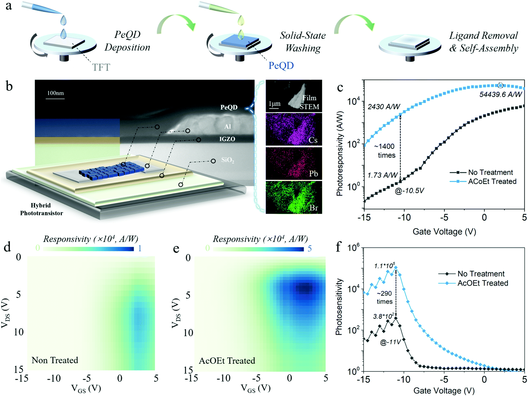 | ||
| Fig. 1 The phototransistor diagram and characterization. (a) Solid-state washing process illustration for the PeQD washing process. (b) Diagram of the PeQD hybrid phototransistor with InGaZnO as the channel layer and PeQDs as the photoactive layer. The right inset figure shows the STEM image of PeQDs with the EDX mapping for the elements, including Cs, Pb, and Br. The cross-section STEM/TEM specimen was prepared by FIB milling. (c) Photoresponsivity of the PeQD hybrid phototransistors versus gate voltage before and after AcOEt treatment, where VDS = 5 V. (d and e) Mapping of the photoresponsivity under various gate and drain voltages (d) before and (e) after solvent treatment. The scale bars are placed above both mappings with different maximum values. All characterization from (c and e) was done with a light wavelength of 475 nm and a power density of 7.73 μW cm−2. (f) Photosensitivity of the hybrid phototransistor before and after AcOEt treatment (VDS = 15 V). | ||
3. Results and discussion
3.1 Medium-polarity-solvent-induced charge transport enhancement of PeQDs
The device structure was demonstrated through a high-angle annular dark-field imaging scanning transmission electron microscopy (HAADF-STEM) cross-section analysis (Fig. 1b) that displays the stacking sequence of the device, Si/SiO2/InGaZnO/Al/PeQDs, with InGaZnO (45 nm) as the channel layer, Al (100 nm) as the drain/source electrode and PeQDs (85 nm) as the photoactive layer. The composition of the PeQDs was confirmed by the HAADF-STEM electron dispersive X-ray (EDX) elemental mapping (Fig. 1b) and the profile elemental line-scan (Fig. S3, ESI†). It could be seen that the PeQDs consist of Cs, Pb, and Br with a proper stoichiometric composition ratio of 1![[thin space (1/6-em)]](https://www.rsc.org/images/entities/char_2009.gif) :1:3. It is worth noting that different anion-coupled PeQDs could exhibit distinct optoelectronic properties. For the sake of consistency, Br was the only anion implemented during our synthesis.29,30 Before studying the stability of the PeQDs during solvent washing, we first investigated the photoresponsivity of the PeQD hybrid phototransistors after solvent treatment to verify that AcOEt washing could promote the charge transport of the PeQD. The measurement was conducted under a 475 nm wavelength light excitation with a power density of 7.73 μW cm−2. Fig. 1b exhibits the good photoresponsivity improvement of the hybrid phototransistor after AcOEt treatment with up to ∼1400 times enhancement (VDS = 5 V, VDS: drain–source voltage). The AcOEt-treated phototransistor exhibited the highest photoresponsivity of 5.4 × 10⁴ A W−1, while the untreated phototransistor had a maximum photoresponsivity of 6.8 × 10³ A W−1 (see Photoresponsivity calculation in ESI†). Furthermore, a comparison of the photoresponsivity at VDS = 15 V presents almost the same ratio of the enhancement (Fig. S4, ESI†). Such a remarkable boost is mainly attributed to a higher density of excited electrons injected from the photoactive layer into the channel layer, which indicates an improved charge transport in the PeQD layer during AcOEt washing.
:1:3. It is worth noting that different anion-coupled PeQDs could exhibit distinct optoelectronic properties. For the sake of consistency, Br was the only anion implemented during our synthesis.29,30 Before studying the stability of the PeQDs during solvent washing, we first investigated the photoresponsivity of the PeQD hybrid phototransistors after solvent treatment to verify that AcOEt washing could promote the charge transport of the PeQD. The measurement was conducted under a 475 nm wavelength light excitation with a power density of 7.73 μW cm−2. Fig. 1b exhibits the good photoresponsivity improvement of the hybrid phototransistor after AcOEt treatment with up to ∼1400 times enhancement (VDS = 5 V, VDS: drain–source voltage). The AcOEt-treated phototransistor exhibited the highest photoresponsivity of 5.4 × 10⁴ A W−1, while the untreated phototransistor had a maximum photoresponsivity of 6.8 × 10³ A W−1 (see Photoresponsivity calculation in ESI†). Furthermore, a comparison of the photoresponsivity at VDS = 15 V presents almost the same ratio of the enhancement (Fig. S4, ESI†). Such a remarkable boost is mainly attributed to a higher density of excited electrons injected from the photoactive layer into the channel layer, which indicates an improved charge transport in the PeQD layer during AcOEt washing.
To have a more in-depth understanding of the effect of the AcOEt treatment on the hybrid phototransistors, we further carried out the two-dimensional (2D) photoresponsivity mapping analysis as a function of the gate and drain voltage (Fig. 1d and e). Similar distribution patterns of the photoresponsivity appear in both mappings with high photoresponsivity around VDS = 5 V and VGS = 2.5 V (VGS: gate–source voltage), where the AcOEt-treated phototransistor possesses much higher photoresponsivity throughout different drain and gate biases (the responsivity scale of Fig. 1e is five times higher than that of Fig. 1d). In both mapping figures, the photoresponsivity increases with the rise of VDS or VGS before reaching the peak value. Within a proper range, the increase of VGS in the positive range attracts more electron injection from the PeQD layer to the InGaZnO channel. Under a higher VDS bias, the injected electrons generate higher drain currents. However, the photoresponsivity of both untreated and treated PeQD phototransistors decreases with a further rise of bias. This is due to the higher probability of scattering and recombination with excessive carrier density.31
In addition to the enhanced photoresponsivity, the photosensitivity (drain current under light/drain current without light) of the AcOEt-treated phototransistor also exhibited a significant enhancement (Fig. 1f). The photosensitivity of both untreated and treated phototransistors peaked at 3.8 × 10² and 1.1 × 10⁵, respectively. The photosensitivity along various power densities was further measured for the AcOEt-treated sample, showing enhanced photosensitivity with increasing laser irradiation power (Fig. S5, ESI†). While the photoresponsivity of the AcOEt-treated phototransistor reached its peak with a gate voltage of ∼2.5 V, its photosensitivity had a different voltage-dependent distribution with the maximum at −10.5 V due to the low dark current. Such a difference in the distribution suggests a trade-off between the photoresponsivity and photosensitivity, where an optimal compromise point between them could be reached by an adequate selection of the gate voltage. Under a different power density, the photosensitivity increases from around 102 at 0.05 μW cm−2 to over 105 at 48.75 μW cm−2, with the peak position of the gate bias almost unchanged. The transfer curve at a different power density of the incident light also shows an increasing photocurrent/dark current ratio with the rise of the power density (Fig. S6, ESI†). Fig. S7a and b (ESI†) present the power response of the photocurrent and photoresponsivity for the AcOEt-treated PeQD phototransistor. The photocurrent as a function of power density was fitted with a power-law equation (y = bxa) before saturation, where a = 0.505 was obtained. Such a low power index of 0.505 indicates the existence of trap states at the surfaces of PeQDs, and the interface between PeQDs and the InGaZnO channel.31 Therefore, the photoresponsivity has a decreasing trend with the rise of the power density, especially after the photocurrent is saturated. The multi-exponential decay of the time-resolved PL (Fig. S7c, ESI†) for both untreated and treated PeQD thin films proves the presence of trap states, consistent with the results in the power response mentioned above.32 Apart from the response under the incident light at 475 nm, the AcOEt-treated hybrid phototransistor has a better characteristic wavelength dependency with the peak responsivity featured at ∼475 nm (Fig. S8, ESI†). To compare this PeQD hybrid phototransistor with previous works, Table S2 (ESI†) summarizes the performance of the PeQD hybrid phototransistors developed in recent studies.
To understand the fundamental physicochemical mechanism behind the enhanced photoresponsivity, we systematically performed Fourier-transform infrared spectroscopy (FTIR) and electron microscopy characterization on the solvent-treated PeQDs. The FTIR transmission spectrum proves the detachment of the OA/OAm ligands with the evidence of the reduction of CH2 peaks at around 2850 cm−1 and 2920 cm−1 (Fig. 2a).33 A quantitative comparison of the vibrational peaks shows that a considerable amount of the aliphatic ligands was removed during the solid-state solvent washing. Fig. 2b illustrates the schematics of charge transport among PeQDs before and after AcOEt washing. With less passivated surfaces, the PeQDs tend to couple with each other and form pathways for better charge transport.18,19
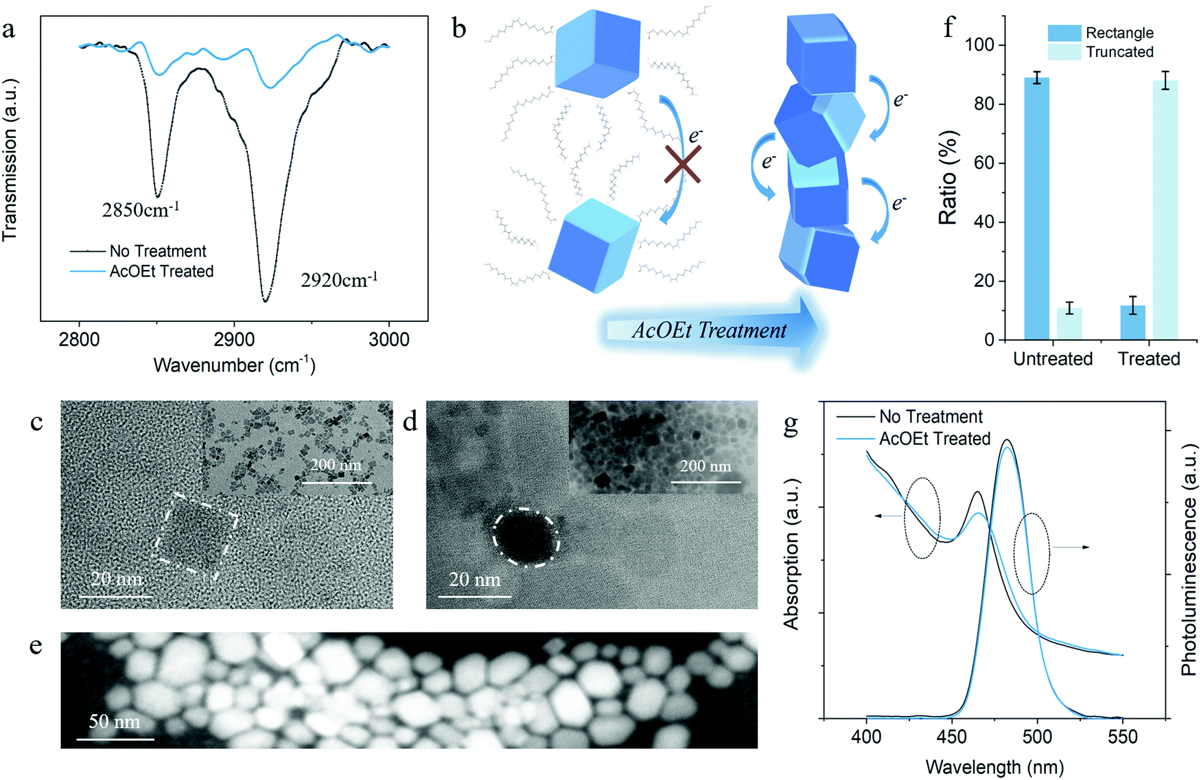 | ||
| Fig. 2 (a) FTIR transmission spectra within 2800 and 3000 cm−1 before (black line) and after (blue line) solvent treatment. (b) Schematics of charge transport improvement induced by AcOEt treatment. (c) and (d) TEM images of the PeQDs (c) before and (d) after AcOEt treatment with the scale bar of 20 nm. The inset figures are the TEM images with a scale of 200 nm. (e) The enlarged HAADF-STEM image of solvent-treated PeQDs. (f) The statistical ratio of the rectangle and truncated nanocrystals in untreated and treated PeQDs. (g) The PL and absorption spectra of the PeQD films before and after AcOEt treatment. | ||
The microscopic images further verify the solvent-induced PeQD coupling and attachment. Fig. 2c and d exhibit the TEM analysis results of the PeQDs before and after the AcOEt treatment, which show that the diameter of the as-prepared PeQDs are around 15 nm. As shown in Fig. 2c and the inset image, the pristine PeQDs exhibit cubic shapes and are well separated from each other by bulky OA/OAm ligands. Additional TEM and HAADF-STEM images of the untreated PeQDs taken in a different area are shown in Fig. S9a and b (ESI†). After AcOEt washing, the PeQDs began to pack together due to the removal of surface passivation with a significant reduction in the dot-to-dot distance, as shown in Fig. 2d.
The inset image of Fig. 2d presents an overview of the densely packed PeQD film (200 nm scale bar). Fig. 2e gives a high-resolution HAADF-STEM image of the solvent (50 nm scale bar), which exhibits the morphology of PeQD. Compared with the STEM image of the untreated PeQDs (Fig. S9c, ESI†), the higher resolution shown in Fig. 2e, in some degree, implies the removal of most surface ligands. The additional HAADF-STEM images of the treated PeQDs in Fig. S9d–f (ESI†) provide further evidence on the evolution of the PeQDs ensemble during the solvent treatment. Under a tightly packed configuration, a strong wavefunction coupling can be established between adjacent PeQDs, which facilitates electron transport in PeQD solid films. Therefore, more electrons can be injected into the InGaZnO channel. This is energetically more efficient than the pristine PeQD ensembles because the insulating ligands block most of the electron transport before reaching the PeQD/InGaZnO interface. The statistical ratio of the rectangle and truncated nanocrystal morphology is shown in Fig. 2f according to the shape distribution of PeQDs in the TEM/STEM images (see statistical ratio counting in ESI†), and indicates that there is a morphology transition after AcOEt treatment (highlighted in Fig. 2c and d). This will be further discussed in the following sections.
To understand the origin of the high photoresponsivity, we need to find out the evolution of the PeQD optical properties during solvent treatment. As shown in Fig. 2g, the solvent treated-PeQD film retained the original optical property well, with only a slight intensity change in both stationary PL and absorption spectra. Indeed, unlike the conventional inorganic quantum dots, PeQDs provide high quantum confinement irrespective of the crystal size or morphology. This is because their intrinsic structure is similar to multiple quantum wells.34–36 The slight reduction in the PL and absorption intensity could be attributed to the stronger coupling of the carrier wavefunction in PeQDs. It was noticed that the PL spectra had a much smaller reduction and red-shift compared with the absorption spectra, which indicate that there is a negligible amount of defect states that are related to non-radiative recombination. This indicates the maintenance of the quantum confinement in PeQDs with inherent excitonic features that enable high photoresponsivity from the as-prepared phototransistors. However, it remains doubtful whether the AcOEt-washed PeQDs become vulnerable under ambient conditions with less passivated surface and changed morphology. Considering the crucial role of the stability of PeQDs in phototransistors, the impact of AcOEt treatment on the ambient durability of PeQDs was further studied. This will be presented in the following paragraph.
3.2 Medium-polarity-solvent-induced stability enhancement of PeQDs
To explore the stability of the PeQD films, we measured the PL spectra for both pristine and solvent-treated PeQD films after 2640 hours storage under ambient condition without light. Fig. 3a shows that the untreated film after storage suffered a more severe PL reduction than the treated sample (Fig. 2e), given the fact that the pristine untreated PeQD film possessed higher PL intensity than the treated one. Moreover, the full width at half maximum (FWHM) of the pristine PeQD film broadened a lot (from ∼27.4 nm to 32 nm) after ambient storage for 2640 hours, while the FWHM of the AcOEt-treated sample was well maintained at ∼27.5 nm under the same storage condition (Fig. 3b). With the solvation and infiltration of water molecules, the structure of PeQDs could be undermined.37 In addition, the untreated PeQDs suffered from severe hydration-assisted nanocrystal aggregation and growth.2 Both degradation mechanisms resulted in PL intensity reduction and quantum confinement weakening, which caused the significant broadening in the FWHM of the untreated PeQD film. On the contrary, minimal change of the treated film's FWHM indicated an enhancement of the PeQD stability during AcOEt treatment, which could be verified by microscopic study and accounted by a marginal reconstruction process in Section 3.3.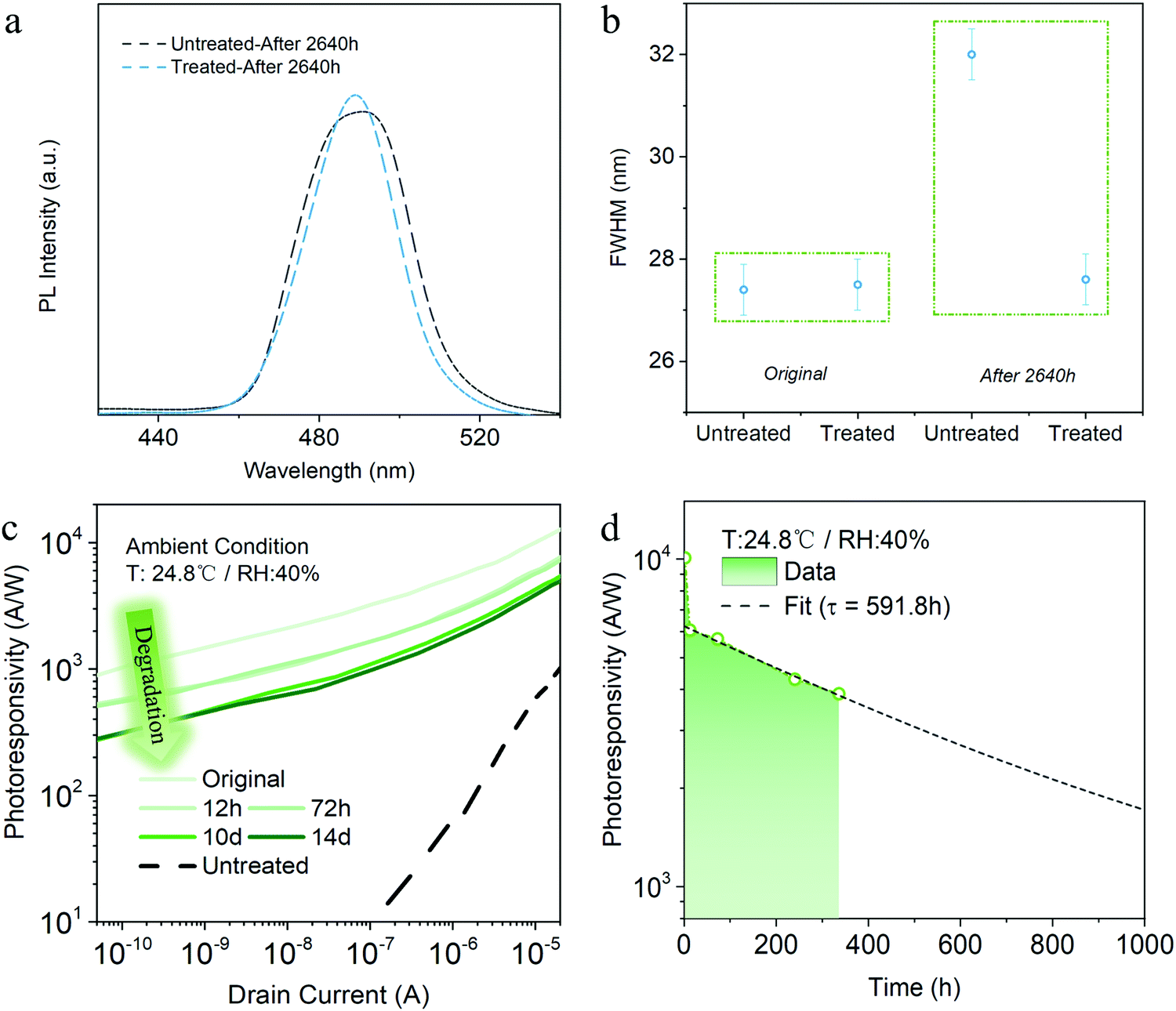 | ||
| Fig. 3 (a) PL spectra of the untreated and treated PeQD films after ambient exposure for 2640 hours. (b) Comparison of the extracted FHWM for pristine and treated PeQD films before and after storage under ambient condition for 2640 h. The error bar stands for the deviation during measurement and parameter extraction. (c) Photoresponsivity versus drain current of the AcOEt-treated phototransistor before storage (original) and after storage for 12 hours, 72 hours, 10 days, and 14 days. (d) Photoresponsivity lifetime analysis of the AcOEt-treated hybrid phototransistor under ambient condition with a drain current of 10 μA. The black dotted line shows the fitting of the second decay of photoresponsivity. | ||
The AcOEt-treated PeQD hybrid phototransistor device lifetime characterization was performed under a benchmark analysis protocol. Typically, to test the stability under ambient atmosphere, we stored devices in the ambient condition without light (24.8 °C and relative humidity of 40%). The photoresponsivity versus gate voltage measured after a specific period is plotted in Fig. 3c. While a remarkable drop of photoresponsivity was noticed during the first 12 hours, no significant degradation was found between 12 hours and 72 hours, as well as between day-10 and day-14. Remarkably, the treated PeQD phototransistor on day-14 still had a much higher photoresponsivity compared to the untreated device on day-1 (dotted line in Fig. 3c), which implies the advantage of AcOEt washing in achieving both high photoresponsivity and robust durability.
Fig. 3d shows the photoresponsivity versus storage time under a drain current of 10 nA, which exhibits a two-phase drop process – a fast decay period before 12 hours, and then a slow decay afterwards. Such a two-phase reduction phenomenon could be attributed to different degradation processes: (i) as mentioned above, part of the ligands remained on the PeQD surface, while some parts of the PeQD surfaces were unpassivated after washing; (ii) in the meantime, some parts of the PeQD surfaces were reconstructed during AcOEt treatment. Therefore, in the first stage, the unpassivated surfaces without reconstruction could degrade in a short time. Afterwards, the remaining parts of the surfaces, including the ligand-passivated and reconstructed ones, might undergo a slower degradation process. The details of the reconstruction process, as well as experimental evidence, will be further explained in the following high-resolution HAADF-STEM microscopic discussions.
Exponential decay (R ∼ exp−t/τ) was used to fit the second stage photoresponsivity decline, where R, t, and τ represent the photoresponsivity, time and decay constant, respectively. It shows that the 1/e lifetime of the treated device is ∼360 hours, and the phototransistor could maintain photoresponsivity over 1000 A W−1 after 1000 hours-exposure in the ambient atmosphere. With such a slow decay, the AcOEt-treated PeQD hybrid phototransistor possessed a considerably long lifetime, one that could potentially be over months. Besides, the declining process showed a similar trend with a drain current of 10 nA or 10 μA (Fig. S10, ESI†), indicating that the photoresponsivity variation came only from the intrinsic degradation of PeQDs.
It is well known that water molecules serve as one of the primary reasons for PeQD destruction.2 Therefore, an extreme condition with 80% humidity (RH 80%) at room temperature was adopted to explore the humidity tolerance of the as-prepared PeQD phototransistors. It should be noted that RH 80% corresponds to the average relative humidity in tropical areas with frequent precipitation, such as Singapore. Typically, the devices were stored in a box with a controlled humidity level without any light, as illustrated in Fig. S11 (ESI†). Fig. S12a (ESI†) shows the photoresponsivity curve versus drain current measured after a different period. Consistent with the fact that PeQDs degrade when exposed to water, the responsivity dropped much faster compared to the deterioration speed under the condition with RH 40% (Fig. S12b, ESI†).2 Nevertheless, even under such an extreme condition and after half a month (360 hours), the solvent-treated phototransistor could still maintain a responsivity value that was close to that of the untreated device before degradation (dotted line). Given the condition that all of our PeQD phototransistors were not encapsulated, it is remarkable to have such a PeQD device lifetime and humidity tolerance for over half a month.
The robust optical property and ambient stability of the ensemble PeQDs indicate that the optoelectronic property of PeQDs, to some degree, mainly depends on the morphology rather than surface ligands. For instance, although the ensemble PeQDs were much closer after the removal of a considerable amount of ligands, the PL and absorption spectra still kept most of their intensity. It meant that the PeQDs maintained their quantum confinement well even though most of the surface ligands had been detached. Furthermore, the ensemble PeQD film surprisingly did not lose ambient stability. Instead, it showed better stability after solvent treatment. All of these results pointed out the significant role of the PeQD morphology in modulating the stability of PeQD.
3.3 Marginal reconstruction of PeQDs during AcOEt treatment
To fully elucidate the relationship between the crystal morphology and material stability, we carried out comprehensive electron microscopy studies on solvent-treated PeQD film and as-prepared phototransistors. According to the azimuthally integrated electron beam diffraction (i-ED) and HRTEM results, it can be seen that during the AcOEt washing process, a solvent-assisted marginal reconstruction occurs at the surface of PeQDs. The i-ED pattern in Fig. 4a implies that multiple facets exist in the untreated PeQDs, including {100}, {111}, {200}, {210} and {300}. This multi-pattern result is consistent with the previously reported nano-twin structures.38,39 Despite the complex structure in PeQD, the facets in the {200} group are exposed at the surface of the untreated PeQD with a cubic morphology (Fig. 4c). After AcOEt washing, the i-ED of the treated PeQDs showed newly generated {110} and {220} patterns in the reciprocal space. The diffraction result is consistent with the HRTEM image of the treated PeQDs, where a new facet group {220} comes up at the PeQD surface (Fig. 4d). This is further supported by the electron diffraction (ED) image of the untreated (Fig. S13, ESI†) and treated PeQDs (Fig. S14, ESI†), where the ED pattern of the treated PeQDs has sharp crystalline spots on the {220} diffraction ring. From this evidence, it can be concluded that a surface-etching process took place during AcOEt washing, where the PeQD surfaces were partially converted from single-facets to multi-facets ({220}, {200}), as presented in the schematic of Fig. 4e.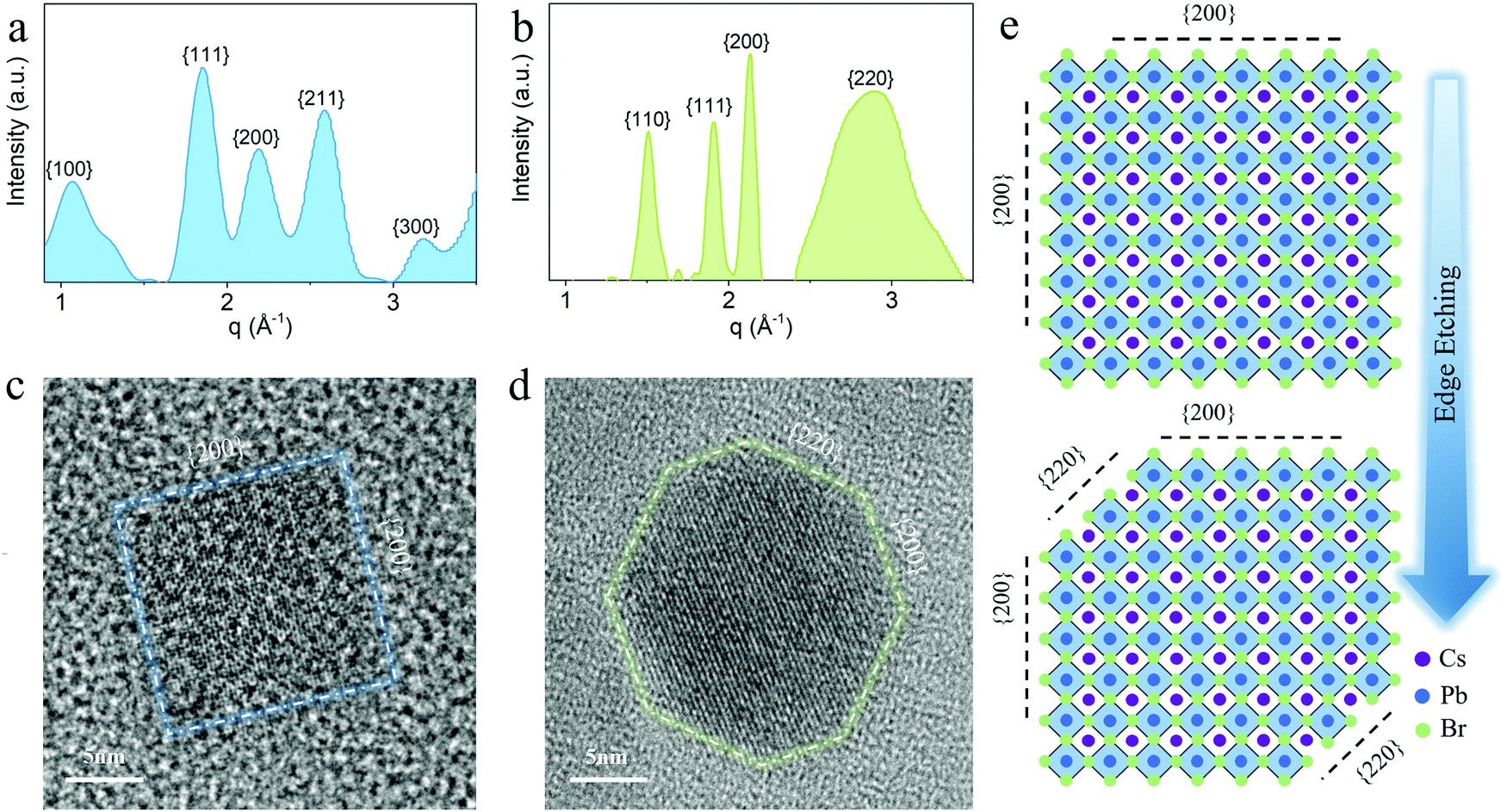 | ||
| Fig. 4 (a) and (b) Azimuthally integrated electron diffraction plot of PeQDs (a) before and (b) after AcOEt treatment. (c) and (d) High-resolution TEM images showing different facets on the surface. (c) For the cubic-shaped PeQD before treatment, the {200} facet group was exposed at the surface, (d) while the {220} group came up after the PeQD was edge-truncated. The glowing dotted lines mark the outlines of two PeQD morphologies. (e) The schematics of the surface edge-etching process from single-facet to multi-facet during AcOEt treatment. | ||
Further electron microscopy studies (Fig. 3) revealed a plausible mechanism of {220} surface evolution through a marginal reconstruction, which occurred right after the surface-etching process. Without the passivation of aliphatic ligands at the surface, the CsPbBr3 PeQD with a cubic-phase is thermodynamically erratic at room temperature, and undergoes a morphology transition to initiate the oriented attachment of unstable facets of PeQDs to form a more stable ensemble structure.18 As captured by the HAADF-STEM analysis (Fig. 5), the edge-truncated PeQDs attached with each other in a dense arrangement. We further validated our consumption via in situ EDX mapping (Fig. S15, ESI†), which confirmed that the particles shown in Fig. 5 are CsPbBr3 PeQDs. An atomic-structure illustration, which highlights the interface between the three attached PeQDs, is shown in Fig. 5, as well as the HAADF-STEM interface fine features (dotted white circle). According to a previous study, the spacing between the QDs linked with the ligands of 10 carbons is over 6 nm.40 Thus, the average spacing of lower than 1 nm (Fig. 5) indicates a close-packed fashion between the PeQDs after the removal of the surface ligands. Based on the HAADF-STEM image, two sorts of interfaces can be indexed: {200} interface and reconstructed {220} interface. When the PeQD surfaces are exposed with the facets of the {220} group, water molecules can infiltrate to interact with the unpassivated Cs atoms, resulting in structural deconstruction. It can be inferred from the HAADF-STEM image that the presence of voids among the PeQDs leaves pathways for water molecules to interact with the {220} facets. However, the direct attachment of {220} facets will facilitate the coordination between Cs and Br, which can help the ‘re-passivation’ of the vulnerable surfaces against the water penetration. Therefore, based on the stable facets in {200} and the assembled facets in the {220} group, the solvent-treated PeQDs realised stable optical and electrical properties under ambient condition.
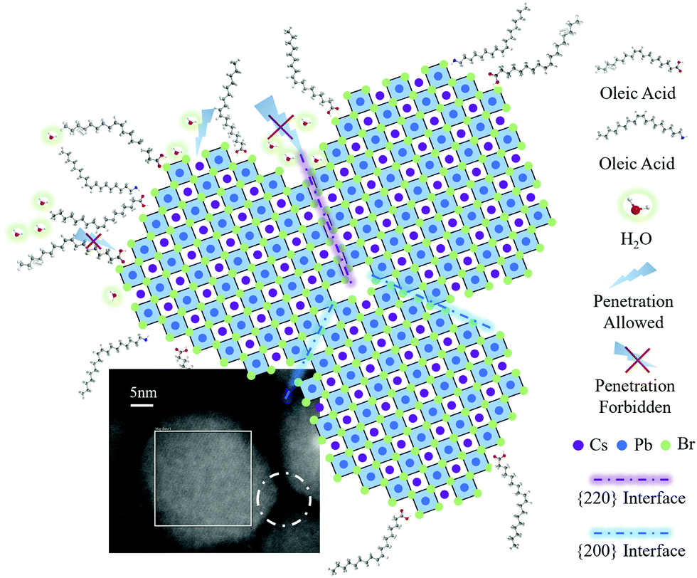 | ||
| Fig. 5 The HAADF-STEM and diagram as the evidence of the PeQD-oriented attachment. The HAADF-STEM image exhibits the direct contact of three AcOEt-treated PeQDs with edge-truncated morphology. The diagram shows the corresponding arrangement of these three PeQDs surrounding the white dotted circle in the HAADF-STEM image (the left one represents the centre PeQD marked with a white box). There are two different interfaces: {220} interface and {200} interface. It is shown that H2O molecules have difficulty infiltrating the {220} interface, which is attributed to the contact between the two facets in the {220} group. | ||
4. Conclusion
In conclusion, we illustrated the fundamental mechanisms of the origin of solvent impacts on the ambient stability of the PeQD material, as well as the operational lifetime of the phototransistor. More importantly, we uncovered a crystal marginal reconstruction process of PeQDs during solvent treatment via AcOEt, a commonly selected medium-polarity solvent. By efficiently detaching the insulating ligands on PeQDs, the photoresponsivity of the solvent-treated hybrid phototransistor showed an enhancement of up to 1400 times, achieving over 5.4 × 10⁴ A W−1 as the maximum, while the highest photosensitivity reached over 105. The HAADF-STEM analysis directly observed the solvent-induced PeQD-coupling, which not only enhanced the charge transport but also preserved the quantum confinement. Apart from the solvent-induced charge transport enhancement, the stability of the PeQD films also showed considerable improvement after AcOEt washing. Stored under an ambient atmosphere with a humidity level of 40% for 2640 hours, the treated PeQD film maintained a much narrower PL FWHM compared to the pristine one. As a result, the AcOEt-treated PeQD hybrid phototransistors obtained a 1/e lifetime of 360 hours, and maintained over 103 A W−1 after 1000 hours. A morphology transition from the cubic shape to an edge-truncated one was captured in the HRTEM and HAADF-STEM analysis. Based on the ED and HRTEM analysis, we found that the {200} group dominated the surface of the untreated PeQDs. At the same time, the edge-truncated PeQDs have newly generated facets in the {220} group. Although facets in {220} tend to have low moisture resistance, a {220} orientated attachment occurred during AcOEt washing, which prevents water penetration and enhances the stability of the PeQD films. Our study yields a new breed of explanation for the role of AcOEt as a medium-polarity solvent to achieve a tightly coupled PeQD film with improved stability and robust phototransistor durability. Moreover, our work reveals the critical role of morphology in PeQDs concerning their optical–electrical property and stability, and introduces a new pathway of perovskite stability enhancement via surface morphology engineering other than the commonly adopted ligand chemistry.Author contributions
S. Z. and B. H. conducted the experiments, collected and interpreted the data, and wrote the manuscript. X. F., J. Z., J. Y., S. B., S. D. H., D. W. S., S. L., and H. W. C. interpreted the data and revised the manuscript. L. G. O. and J. M. K. guided the work, provided research infrastructure support and revised the manuscript.Conflicts of interest
There are no conflicts to declare.Acknowledgements
The authors acknowledge the support from the European Union under the H2020 project 1D-NEON (Grant Agreement No. 685758), and from the Engineering and Physical Sciences Research Council (EPSRC) in the UK under the project SmartQD (EP/P027628/1). We especially acknowledge the discussion and support provided by Felix C. Mocanu.References
- L. Protesescu, S. Yakunin, M. I. Bodnarchuk, F. Krieg, R. Caputo, C. H. Hendon, R. X. Yang, A. Walsh and M. V. Kovalenko, Nano Lett., 2015, 15, 3692–3696 CrossRef.
- H. C. Wang, Z. Bao, H. Y. Tsai, A. C. Tang and R. S. Liu, Small, 2018, 14(1), 1702433 CrossRef.
- Y. Kim, E. Yassitepe, O. Voznyy, R. Comin, G. Walters, X. Gong, P. Kanjanaboos, A. F. Nogueira and E. H. Sargent, ACS Appl. Mater. Interfaces, 2015, 7, 25007–25013 CrossRef.
- J. Song, J. Li, X. Li, L. Xu, Y. Dong and H. Zeng, Adv. Mater., 2015, 27, 7162–7167 CrossRef.
- Y. Chen, Y. Chu, X. Wu, W. Ou-Yang and J. Huang, Adv. Mater., 2017, 29(44), 1704062 CrossRef.
- B. Hou, Isr. J. Chem., 2019, 59, 637–638 CrossRef CAS.
- Y. Zhao, J. Li, Y. Dong and J. Song, Isr. J. Chem., 2019, 59, 649–660 CrossRef CAS.
- B. Li, M. Lu, J. Feng, J. Zhang, P. M. Smowton, J. I. Sohn, I.-K. Park, H. Zhong and B. Hou, J. Mater. Chem. C, 2020, 8, 10676–10695 RSC.
- Y. Chen, Y. Chu, X. Wu, W. Ou-Yang and J. Huang, Adv. Mater., 2017, 29, 1704062 CrossRef.
- C. Zou, Y. Xi, C. Y. Huang, E. G. Keeler, T. Feng, S. Zhu, L. D. Pozzo and L. Y. Lin, Adv. Opt. Mater., 2018, 6(14), 1800324 CrossRef.
- D. K. Hwang, Y. T. Lee, H. S. Lee, Y. J. Lee, S. H. Shokouh, J.-H. Kyhm, J. Lee, H. H. Kim, T.-H. Yoo, S. H. Nam, D. I. Son, B.-K. Ju, M.-C. Park, J. D. Song, W. K. Choi and S. Im, NPG Asia Mater., 2016, 8, e233 CrossRef CAS.
- M. Chen, H. Lu, N. M. Abdelazim, Y. Zhu, Z. Wang, W. Ren, S. V. Kershaw, A. L. Rogach and N. Zhao, ACS Nano, 2017, 11, 5614–5622 CrossRef CAS.
- C. Y. Wu, Z. Wang, L. Liang, T. Gui, W. Zhong, R. C. Du, C. Xie, L. Wang and L. B. Luo, Small, 2019, 15, 1900730 CrossRef.
- Y. Yang, H. Dai, F. Yang, Y. Zhang, D. Luo, X. Zhang, K. Wang, X. W. Sun and J. Yao, Nanoscale Res. Lett., 2019, 14, 1–8 CrossRef.
- F. Li, C. Ma, H. Wang, W. Hu, W. Yu, A. D. Sheikh and T. Wu, Nat. Commun., 2015, 6, 8238 CrossRef.
- J. Z. Fan, N. T. Andersen, M. Biondi, P. Todorović, B. Sun, O. Ouellette, J. Abed, L. K. Sagar, M. J. Choi and S. Hoogland, Adv. Mater., 2019, 31, 1904304 CrossRef CAS.
- J. Kim, S.-M. Kwon, Y. K. Kang, Y.-H. Kim, M.-J. Lee, K. Han, A. Facchetti, M.-G. Kim and S. K. Park, Sci. Adv., 2019, 5, eaax8801 CrossRef CAS.
- J.-K. Sun, S. Huang, X.-Z. Liu, Q. Xu, Q.-H. Zhang, W.-J. Jiang, D.-J. Xue, J.-C. Xu, J.-Y. Ma and J. Ding, J. Am. Chem. Soc., 2018, 140, 11705–11715 CrossRef CAS.
- N. Soetan, W. R. Erwin, A. M. Tonigan, D. G. Walker and R. Bardhan, J. Phys. Chem. C, 2017, 121, 18186–18194 CrossRef.
- L. Wang, B. Liu, X. Zhao, H. V. Demir, H. Gu and H. Sun, ACS Appl. Mater. Interfaces, 2018, 10, 19828–19835 CrossRef.
- T. Chiba, K. Hoshi, Y. J. Pu, Y. Takeda, Y. Hayashi, S. Ohisa, S. Kawata and J. Kido, ACS Appl. Mater. Interfaces, 2017, 9, 18054–18060 CrossRef.
- L. Zhou, K. Yu, F. Yang, H. Cong, N. Wang, J. Zheng, Y. Zuo, C. Li, B. Cheng and Q. Wang, J. Mater. Chem. C, 2017, 5, 6224–6233 RSC.
- K. Hoshi, T. Chiba, J. Sato, Y. Hayashi, Y. Takahashi, H. Ebe, S. Ohisa and J. Kido, ACS Appl. Mater. Interfaces, 2018, 10, 24607–24612 CrossRef.
- M. Leng, Y. Yang, K. Zeng, Z. Chen, Z. Tan, S. Li, J. Li, B. Xu, D. Li and M. P. Hautzinger, Adv. Funct. Mater., 2018, 28, 1704446 CrossRef.
- S. Wang, C. Bi, J. Yuan, L. Zhang and J. Tian, ACS Energy Lett., 2017, 3, 245–251 CrossRef.
- H. Yang, Y. Feng, Z. Tu, K. Su, X. Fan, B. Liu, Z. Shi, Y. Zhang, C. Zhao and B. Zhang, Nano Res., 2019, 12, 3129–3134 CrossRef CAS.
- X. Li, Y. Wu, S. Zhang, B. Cai, Y. Gu, J. Song and H. Zeng, Adv. Funct. Mater., 2016, 26, 2435–2445 CrossRef CAS.
- S. Zhan, S. Han, S. Y. Bang, B. Li, Y. T. Chun, B. Hou and J. M. Kim, Phys. Status Solidi A, 2020, 217(12), 1900832 CrossRef CAS.
- T. Chiba, Y. Hayashi, H. Ebe, K. Hoshi, J. Sato, S. Sato, Y.-J. Pu, S. Ohisa and J. Kido, Nat. Photonics, 2018, 12, 681–687 CrossRef CAS.
- Y. Zhai, X. Bai, G. Pan, J. Zhu, H. Shao, B. Dong, L. Xu and H. Song, Nanoscale, 2019, 11, 2484–2491 RSC.
- H. Wu, H. Si, Z. Zhang, Z. Kang, P. Wu, L. Zhou, S. Zhang, Z. Zhang, Q. Liao and Y. Zhang, Adv. Sci., 2018, 5, 1801219 CrossRef.
- Y. Li, X. Hou, X. Dai, Z. Yao, L. Lv, Y. Jin and X. Peng, J. Am. Chem. Soc., 2019, 141, 6448–6452 CrossRef CAS.
- Y.-H. Suh, T. Kim, J. W. Choi, C.-L. Lee and J. Park, ACS Appl. Nano Mater., 2018, 1, 488–496 CrossRef CAS.
- Y. H. Kim, H. Cho, J. H. Heo, T. S. Kim, N. Myoung, C. L. Lee, S. H. Im and T. W. Lee, Adv. Mater., 2015, 27, 1248–1254 CrossRef CAS.
- Z. K. Tan, R. S. Moghaddam, M. L. Lai, P. Docampo, R. Higler, F. Deschler, M. Price, A. Sadhanala, L. M. Pazos, D. Credgington, F. Hanusch, T. Bein, H. J. Snaith and R. H. Friend, Nat. Nanotechnol., 2014, 9, 687–692 CrossRef CAS.
- H. Cho, S.-H. Jeong, M.-H. Park, Y.-H. Kim, C. Wolf, C.-L. Lee, J. H. Heo, A. Sadhanala, N. Myoung and S. Yoo, Science, 2015, 350, 1222–1225 CrossRef CAS.
- E. Mosconi, J. M. Azpiroz and F. De Angelis, Chem. Mater., 2015, 27, 4885–4892 CrossRef CAS.
- F. Bertolotti, L. Protesescu, M. V. Kovalenko, S. Yakunin, A. Cervellino, S. J. Billinge, M. W. Terban, J. S. Pedersen, N. Masciocchi and A. Guagliardi, ACS Nano, 2017, 11, 3819–3831 CrossRef CAS.
- N. Kattan, B. Hou, D. J. Fermín and D. Cherns, Appl. Mater. Today, 2015, 1, 52–59 CrossRef.
- L. Sun, J. J. Choi, D. Stachnik, A. C. Bartnik, B. R. Hyun, G. G. Malliaras, T. Hanrath and F. W. Wise, Nat. Nanotechnol., 2012, 7, 369–373 CrossRef CAS.
Footnote |
| † Electronic supplementary information (ESI) available: Detailed experimental procedures and supporting images. See DOI: 10.1039/d0tc03838e |
| This journal is © The Royal Society of Chemistry 2020 |